EP3916931B1 - Plug connector slidably inserted into receptacle connector - Google Patents
Plug connector slidably inserted into receptacle connector Download PDFInfo
- Publication number
- EP3916931B1 EP3916931B1 EP21174678.9A EP21174678A EP3916931B1 EP 3916931 B1 EP3916931 B1 EP 3916931B1 EP 21174678 A EP21174678 A EP 21174678A EP 3916931 B1 EP3916931 B1 EP 3916931B1
- Authority
- EP
- European Patent Office
- Prior art keywords
- shield
- signal pin
- connector
- section
- signal
- Prior art date
- Legal status (The legal status is an assumption and is not a legal conclusion. Google has not performed a legal analysis and makes no representation as to the accuracy of the status listed.)
- Active
Links
Images






Classifications
-
- H—ELECTRICITY
- H01—ELECTRIC ELEMENTS
- H01R—ELECTRICALLY-CONDUCTIVE CONNECTIONS; STRUCTURAL ASSOCIATIONS OF A PLURALITY OF MUTUALLY-INSULATED ELECTRICAL CONNECTING ELEMENTS; COUPLING DEVICES; CURRENT COLLECTORS
- H01R13/00—Details of coupling devices of the kinds covered by groups H01R12/70 or H01R24/00 - H01R33/00
- H01R13/648—Protective earth or shield arrangements on coupling devices, e.g. anti-static shielding
- H01R13/658—High frequency shielding arrangements, e.g. against EMI [Electro-Magnetic Interference] or EMP [Electro-Magnetic Pulse]
- H01R13/6581—Shield structure
- H01R13/6585—Shielding material individually surrounding or interposed between mutually spaced contacts
- H01R13/6589—Shielding material individually surrounding or interposed between mutually spaced contacts with wires separated by conductive housing parts
-
- H—ELECTRICITY
- H01—ELECTRIC ELEMENTS
- H01R—ELECTRICALLY-CONDUCTIVE CONNECTIONS; STRUCTURAL ASSOCIATIONS OF A PLURALITY OF MUTUALLY-INSULATED ELECTRICAL CONNECTING ELEMENTS; COUPLING DEVICES; CURRENT COLLECTORS
- H01R12/00—Structural associations of a plurality of mutually-insulated electrical connecting elements, specially adapted for printed circuits, e.g. printed circuit boards [PCB], flat or ribbon cables, or like generally planar structures, e.g. terminal strips, terminal blocks; Coupling devices specially adapted for printed circuits, flat or ribbon cables, or like generally planar structures; Terminals specially adapted for contact with, or insertion into, printed circuits, flat or ribbon cables, or like generally planar structures
- H01R12/70—Coupling devices
- H01R12/71—Coupling devices for rigid printing circuits or like structures
- H01R12/75—Coupling devices for rigid printing circuits or like structures connecting to cables except for flat or ribbon cables
-
- H—ELECTRICITY
- H01—ELECTRIC ELEMENTS
- H01R—ELECTRICALLY-CONDUCTIVE CONNECTIONS; STRUCTURAL ASSOCIATIONS OF A PLURALITY OF MUTUALLY-INSULATED ELECTRICAL CONNECTING ELEMENTS; COUPLING DEVICES; CURRENT COLLECTORS
- H01R13/00—Details of coupling devices of the kinds covered by groups H01R12/70 or H01R24/00 - H01R33/00
- H01R13/46—Bases; Cases
- H01R13/502—Bases; Cases composed of different pieces
-
- H—ELECTRICITY
- H01—ELECTRIC ELEMENTS
- H01R—ELECTRICALLY-CONDUCTIVE CONNECTIONS; STRUCTURAL ASSOCIATIONS OF A PLURALITY OF MUTUALLY-INSULATED ELECTRICAL CONNECTING ELEMENTS; COUPLING DEVICES; CURRENT COLLECTORS
- H01R13/00—Details of coupling devices of the kinds covered by groups H01R12/70 or H01R24/00 - H01R33/00
- H01R13/62—Means for facilitating engagement or disengagement of coupling parts or for holding them in engagement
- H01R13/629—Additional means for facilitating engagement or disengagement of coupling parts, e.g. aligning or guiding means, levers, gas pressure electrical locking indicators, manufacturing tolerances
-
- H—ELECTRICITY
- H01—ELECTRIC ELEMENTS
- H01R—ELECTRICALLY-CONDUCTIVE CONNECTIONS; STRUCTURAL ASSOCIATIONS OF A PLURALITY OF MUTUALLY-INSULATED ELECTRICAL CONNECTING ELEMENTS; COUPLING DEVICES; CURRENT COLLECTORS
- H01R13/00—Details of coupling devices of the kinds covered by groups H01R12/70 or H01R24/00 - H01R33/00
- H01R13/648—Protective earth or shield arrangements on coupling devices, e.g. anti-static shielding
- H01R13/658—High frequency shielding arrangements, e.g. against EMI [Electro-Magnetic Interference] or EMP [Electro-Magnetic Pulse]
- H01R13/6581—Shield structure
-
- H—ELECTRICITY
- H01—ELECTRIC ELEMENTS
- H01R—ELECTRICALLY-CONDUCTIVE CONNECTIONS; STRUCTURAL ASSOCIATIONS OF A PLURALITY OF MUTUALLY-INSULATED ELECTRICAL CONNECTING ELEMENTS; COUPLING DEVICES; CURRENT COLLECTORS
- H01R24/00—Two-part coupling devices, or either of their cooperating parts, characterised by their overall structure
- H01R24/60—Contacts spaced along planar side wall transverse to longitudinal axis of engagement
- H01R24/62—Sliding engagements with one side only, e.g. modular jack coupling devices
-
- H—ELECTRICITY
- H01—ELECTRIC ELEMENTS
- H01R—ELECTRICALLY-CONDUCTIVE CONNECTIONS; STRUCTURAL ASSOCIATIONS OF A PLURALITY OF MUTUALLY-INSULATED ELECTRICAL CONNECTING ELEMENTS; COUPLING DEVICES; CURRENT COLLECTORS
- H01R9/00—Structural associations of a plurality of mutually-insulated electrical connecting elements, e.g. terminal strips or terminal blocks; Terminals or binding posts mounted upon a base or in a case; Bases therefor
- H01R9/03—Connectors arranged to contact a plurality of the conductors of a multiconductor cable, e.g. tapping connections
- H01R9/05—Connectors arranged to contact a plurality of the conductors of a multiconductor cable, e.g. tapping connections for coaxial cables
- H01R9/0524—Connection to outer conductor by action of a clamping member, e.g. screw fastening means
-
- H—ELECTRICITY
- H01—ELECTRIC ELEMENTS
- H01R—ELECTRICALLY-CONDUCTIVE CONNECTIONS; STRUCTURAL ASSOCIATIONS OF A PLURALITY OF MUTUALLY-INSULATED ELECTRICAL CONNECTING ELEMENTS; COUPLING DEVICES; CURRENT COLLECTORS
- H01R2103/00—Two poles
-
- H—ELECTRICITY
- H01—ELECTRIC ELEMENTS
- H01R—ELECTRICALLY-CONDUCTIVE CONNECTIONS; STRUCTURAL ASSOCIATIONS OF A PLURALITY OF MUTUALLY-INSULATED ELECTRICAL CONNECTING ELEMENTS; COUPLING DEVICES; CURRENT COLLECTORS
- H01R24/00—Two-part coupling devices, or either of their cooperating parts, characterised by their overall structure
- H01R24/60—Contacts spaced along planar side wall transverse to longitudinal axis of engagement
- H01R24/62—Sliding engagements with one side only, e.g. modular jack coupling devices
- H01R24/64—Sliding engagements with one side only, e.g. modular jack coupling devices for high frequency, e.g. RJ 45
Definitions
- the following description relates to a connector, and more particularly, to a plug connector that is slidably inserted into a receptacle connector.
- a connector assembly including a receptacle connector and a plug connector is used to connect the circuit board to another electronic device or another circuit board.
- the receptacle connector is mounted on the circuit board, the plug connector is coupled to a cable, and the plug connector is coupled to the receptacle connector, so that the cable and the circuit board are electrically connected.
- Conventional connector assemblies have a structure in which a plug connector is vertically fastened to a receptacle connector with respect to a circuit board. Accordingly, it is difficult to miniaturize the connector assembly due to the height of the connector assembly and fastening copper wires of the plug connector, and such a structure is unfavorable in shielding electromagnetic waves. Also, it is difficult to simultaneous connect a plurality of cables and a circuit board with a single connector assembly.
- EP 0 833 405 A1 discloses a plug connector that is slidably inserted into a receptacle connector.
- a signal pin of the plug connector has one side in electrical contact with one side of a a cable's signal line.
- a shield can is electrically spaced apart from the signal pin and surrounds the signal pin such that a lower surface of the other side of the signal pin is exposed.
- a first insulating member is coupled to the signal pin to insulate the signal pin and the shield can from each other.
- a plug shell is shown that surrounds the shield can such that the lower surface of the other side of the signal pin is exposed.
- US 2012/264337 A1 discloses an assembly which is formed by an electrical wire a plug housing.
- An objective of the present invention is to provide a structure in which a plug connector is slidably inserted into a receptacle connector, which is favorable for miniaturization of a connector assembly by allowing the height of the connector assembly to be reduced and making a fastening copper wire of the plug connector parallel to a circuit board.
- another objective of the present invention is to provide a plug connector which provides excellent electromagnetic wave shielding performance and is capable of simultaneously connecting a plurality of cables and a circuit board.
- the shield can includes a lower shield can having a seating groove in which a lower portion of the cable is seated and an upper shield can having a seating groove in which an upper portion of the cable is seated and covering the lower shield can.
- a plurality of signal pins may be arranged in parallel to each other corresponding to a plurality of cables, and the shield can may include a shielding wall that shields between adjacent signal pins.
- the signal pin includes a first portion on one side thereof which has an insertion portion into which the signal line is inserted and a second portion on the other side thereof which is formed integrally with the first portion and has the lower surface of the other side.
- the first insulating member has a through hole through which the second portion of the signal pin passes, and may include a first section that forms an upper portion of the through hole and is formed to expose the lower surface of the other side of the second portion while covering an upper portion of the second portion; and a second section that forms a lower portion of the through hole and is formed below the first section to be shorter than the first section such that the lower surface of the other side of the second portion is exposed.
- the shield includes a lower shield can having a seating groove in which a lower portion of the cable is seated and a seating groove in which the second section of the first insulating member is seated; and an upper shield can covering the lower shield can and having a seating groove in which an upper portion of the cable is seated and a seating groove in which the first section of the first insulating member is seated.
- the plug shell may be formed of a metal material.
- the plug shell may have an enclosing portion that encloses and supports a portion of the cable exposed to the outside of the shield can.
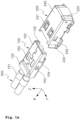
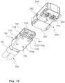
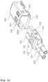
- FIGS. 1A to 1C are views of a connector assembly according to an embodiment of the present invention.
- the positive X-axis direction is defined as a forward direction (or a front side or a front end) and the negative X-axis direction is a rearward direction (or a rear side or a rear end).
- the positive Z-axis direction is defined as an upper direction (or an upper surface or an upper end) and the negative Z-axis direction is a lower direction (or a lower surface or a lower end).
- the positive and negative Y-axis directions are defined as a lateral direction.
- FIG. 1A is a perspective view of the connector assembly as viewed from the upper rear side thereof
- FIG. 1B is a perspective view of the connector assembly as viewed from the lower rear side thereof
- FIG. 1C is a perspective view of the connector assembly as viewed from the upper front side thereof.
- the connector assembly includes a receptacle connector 200 mounted on a circuit board (which is designated by reference P in FIG. 6C ), and a plug connector 100 to be coupled to a cable 300 and slidably inserted into the receptacle connector 200.
- the receptacle connector 200 may be mounted on the circuit board P using a surface mount method, such as surface mount device (SMD) or surface mount technology (SMT), a through-hole method, such as single in-line package (SIP), dual in-line package (DIP), quad in-line package (QIP), or the like, or both the surface mount method and the through-hole method.
- a surface mount method such as surface mount device (SMD) or surface mount technology (SMT)
- SMT surface mount technology
- a through-hole method such as single in-line package (SIP), dual in-line package (DIP), quad in-line package (QIP), or the like, or both the surface mount method and the through-hole method.
- the receptacle connector 200 may not be a separate component but may be integrally formed with the circuit board P.
- the receptacle connector 200 may have a shape in which the front end is open and the rear end is closed so that the plug connector 100 can be slidably inserted from the front end.
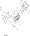
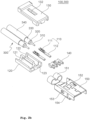
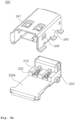
- FIGS. 2A to 2C are views of the plug connector 100 according to an embodiment of the present invention.
- FIG. 2A is a first exploded view of the plug connector 100 as viewed from the upper rear side thereof
- FIG. 2B is a second exploded view of the plug connector 100 as viewed from the upper rear side thereof
- FIG. 2C is a view of the plug connector 100 shown in FIG. 2B , when viewed from the lower rear side.
- a coaxial cable is described as an example of the cable 300 coupled to the plug connector 100, but the cable 300 may be any of various types of cables, such as a data cable, a wire, a flexible flat cable (FFC), a flexible printed circuit (FPC), and the like, instead of the coaxial cable.
- a data cable such as a data cable, a wire, a flexible flat cable (FFC), a flexible printed circuit (FPC), and the like, instead of the coaxial cable.
- FFC flexible flat cable
- FPC flexible printed circuit
- the cable 300 may include a signal line (internal conductor) 310, an outer conductor 330 made of aluminum, copper, etc. which shields electromagnetic waves of the signal line 310, a dielectric material 320 that insulates and separates the signal line 310 and the outer conductor 330 from each other, and a jacket 340 that protects the outer conductor 330.
- a signal line internal conductor
- an outer conductor 330 made of aluminum, copper, etc. which shields electromagnetic waves of the signal line 310
- a dielectric material 320 that insulates and separates the signal line 310 and the outer conductor 330 from each other
- a jacket 340 that protects the outer conductor 330.
- the plug connector 100 includes signal pins 110, shield cans 120 and 130, a first insulating member 140, and a plug shell 150.
- the number of cables 300 may be one or three or more. When there is a plurality of cables 300, the cables 300 are disposed in parallel to each other. Those skilled in the art will understand that the number or structures of the signal pins 110, the shield cans 120 and 130, the first insulating members 140, and the plug shells 150 may be appropriately modified according to the number of cables 300.
- the signal pin 110 may be formed such that a front end thereof is in electrical contact with the signal line 310 of the cable 300 and a lower surface 112a of a rear side thereof is in elastic contact with an upper side of a clip pin 210 of the receptacle connector 200 which will be described below.
- the signal pin 110 is provided for each cable 300, and when there is a plurality of cables 300, a plurality of signal pins 110 are also arranged in parallel to each other.
- the signal pin 110 includes a first portion 111 at the front side and a second portion 112 integrally formed at the rear side with the first portion 111.
- the first portion 111 includes an insertion portion into which the signal line 310 is inserted.
- the first portion 111 of the signal pin 110 and the signal line 310 may be in electrical contact with each other by tightening or soldering.
- One or more protrusions may be formed inside the first portion 111 of the signal pin 110 to improve tensile force for fixing the signal line 310.
- the second portion 112 has a lower surface 112a in elastic contact with an upper portion of the clip pin 210 of the receptacle connector 200.
- the shield cans 120 and 130 surround the signal pin 110 so that the lower surface 112a of the second portion 112 of the signal pin 110 is exposed, and are formed to be electrically spaced apart from the signal pin 110.
- the shield cans 120 and 130 may be formed of a metal material to shield electromagnetic waves.
- the shield cans 120 and 130 includes a lower shield can 120 and an upper shield can 130.
- the lower shield can 120 includes a seating groove 121 in which the lower portion of the cable 300 is seated.
- the upper shield can 130 is formed to cover the lower shield can 120 and has a seating groove 131 in which an upper portion of the cable 300 is seated.
- the shield cans 120 and 130 are described as being formed by combining the lower shield can 120 and the upper shield can 130, but the shield cans 120 and 130 may be integrally formed as a unitary structure.
- the lower shield can 120 may include a shielding wall 122 that shields between adjacent signal pins 110.
- the upper shield can 130 may include a hole 132 into which an upper portion of the shielding wall 122 is inserted.
- the shielding wall that shields between adjacent signal pins 110 may be provided on the upper shield can 130 instead of the lower shield can 120.
- FIGS. 3A to 3C are views specifically illustrating the signal pins 110 and the first insulating member 140.
- FIG. 3A is a view of the signal pins 110 and the first insulating member 140, when viewed from the lower rear side
- FIG. 3B is a view illustrating a state in which the signal pins 110 and the first insulating member 140 are separated from each other
- FIG. 3C is a view illustrating the signal pins 110 and the first insulating member 140 shown in FIG. 3B , when viewed from the upper front side.
- the first insulating member 140 has a through hole 141 through which the second portion 112 of the signal pin 110 passes, and consists of a first section 142 and a second section 143 that may be integrally formed with the first section 142.
- the through hole 141, the first section 142, and the second section 143 are provided for each signal pin 110.
- the first section 142 forms an upper portion of the through hole 141 and is elongated along a length direction of the second portion 112 such that it covers an upper portion of the second portion 112 of the signal pin 110 and exposes the lower surface 112a of the second portion 112.
- the second section 143 forms a lower portion of the through hole 141 and is formed below the first section 142 to be shorter than the first section 142 along the length direction of the second portion 112 such that the lower surface 112a of the second portion 112 of the signal pin 110 is exposed.
- the lower shield can 120 has a seating groove 123 in which the second section 143 of the first insulating member 140 is seated.
- the upper shield can 130 includes a seating groove 133 in which the first section 142 of the first insulating member 140 is seated.
- the plug shell 150 surrounds the upper, lower, and both lateral surfaces of the shield cans 120 and 130 (specifically, the upper surface and both lateral surfaces of the upper shield can 130 and the lower surface and both lateral surfaces of the lower shield can 120) such that the lower surface 112a of the second portion 112 of the signal pin 110 is exposed.
- the plug shell 150 may be formed of a metal material for shielding electromagnetic waves. Also, the plug shell 150 may include an enclosing portion that encloses and supports a part of the cable 300 exposed to the outside of the shield cans 120 and 130 in front of the shield cans 120 and 130. The enclosing portion 151 may extend in the front direction from the lower portion of the plug shell 150. The enclosing portion 151 may prevent damage due to excessive bending or separation of the cable 300.
- electromagnetic waves generated through the signal line 310 and the outer conductor 330 of the cable 300 and the signal pin 110 are primarily shielded by the shield cans 120 and 130 and secondarily shielded by the plug shell 150, thus improving electromagnetic wave shielding performance.
- electromagnetic waves between adjacent signal lines 310 or between adjacent signal pins 110 are shielded by the shielding walls 122 in the shield cans 120 and 130, interference between signals may be minimized.
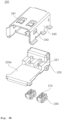
- FIGS. 4A to 4C are views of a receptacle connector 200 into which a plug connector 100 according to an embodiment of the present invention is slidably inserted.
- FIG. 4A is a first exploded view of the receptacle connector 200 viewed from the upper front side thereof
- FIG. 4B is a second exploded view of the receptacle connector 200 viewed from the upper front side thereof
- FIG. 4C is a view of the receptacle connector 200 shown in FIG. 4B when viewed from the lower front side.
- the receptacle connector 200 includes a clip pin 210, a receptacle base 220, a second insulating member 230, and a receptacle shell 240.
- the clip pin 210 may be formed such that a lower surface thereof is in electrical contact with a signal pad (not shown) of a circuit board (which is designated by reference P in FIG. 6c ) through elastic contact or soldering and an upper portion thereof is in elastic contact with the lower surface 112a of the second portion 112 of the signal pin 110.
- the electrical contact of the clip pin 210 may be made by a surface mount method, such as SMD o r SMT, a through-hole method, such as SIP, DIP, and QIP, or the like.
- a surface mount method such as SMD o r SMT
- a through-hole method such as SIP, DIP, and QIP, or the like.
- the receptacle base 220 is installed on an upper surface of the substrate P, and provides a space 221 in which the second insulating member 230 and the clip pin 210 are accommodated.
- the space 221 may be formed to penetrate the top and bottom of the receptacle base 220.
- the second insulating member 230 is inserted into the space 221 of the receptacle base 220 and surrounds the clip pin 210 from the side to fix the clip pin 2 1 0 and simultaneously insulate the clip pin 210 from the receptacle base 220.
- the receptacle shell 240 covers the receptacle base 220 and provides a space in which the plug connector 100 is slidably inserted together with the receptacle base 220. That is, the plug connector 100 is slidably inserted into the space defined by an upper surface 220a of the receptacle base 220 and an inner upper surface and both inner lateral surfaces of the receptacle shell 240.
- the receptacle base 220 and the receptacle shell 240 may be formed of a metal material to shield electromagnetic waves.
- electromagnetic waves generated through the signal line 310, the outer conductor 330, and the signal pin 110 are primarily shielded by the shield cans 120 and 130, secondarily shielded by the plug shell 150, and tertiarily shielded by the receptacle base 220 and the receptacle Shell 240.
- the plug shell 150 may have a fastening hole 152 on the upper surface, and the receptacle shell 240 may have an elastic fastening portion 241 on the upper surface, which is inserted and fastened into the fastening hole 152.
- the receptacle shell 240 may include fastening holes 242 on both sides thereof, and the plug shell 150 may include fastening protrusions 153 on both sides thereof, which are inserted and fastened into the fastening holes 242.
- the plug shell 150 may have protrusions 154 on both sides thereof, and the projections 154 are in close contact with both inner sides of the receptacle shell 240.
- the plug shell 150 has a plurality of protrusions 155 (for example, at four points on front, rear, and both sides) on a lower surface 50a thereof, and the protrusions 155 are in close contact with the upper surface 220a of the receptacle base 220.
- FIG. 5 is a view illustrating a state in which the clip pin 210 and the second insulating member 230 of the receptacle connector 200 are separated from each other.
- the clip pin 210 may include a first section 211 having a lower surface in contact with the signal pad of the circuit board P, a second section 212 extending substantially upward from a front end of the first section 211, a third section 213 extending substantially rearward from an upper end of the second section 212, a fourth section 214 extending obliquely forward and upward from a rear end of the third section 213, and a fifth section 215 extending obliquely forward and downward from an upper end of the fourth section 214.
- a lower surface of the first section 211 may be in elastic contact with the signal pad of the circuit board P, and an upper portion of the clip pin 210, that is, a portion between the fourth section 214 and the fifth section 215, may be in elastic contact with the lower surface 112a of the second portion 112 of the signal pin 110.
- the electrical contact of the lower surface of the first section 211 of the clip pin 210 may be made by a surface mount method, such as SMD or SMT, a through-hole method, such as SIP, DIP, and QIP, or the like.
- the clip pin 210 is disposed so that the fifth section 215 faces forward, but the clip pin 210 may be disposed so that the fifth section 214 faces rearward.
- the second insulating member 230 may have a through hole 231 penetrating vertically to accommodate the clip pin 210.
- the second insulating member 230 may have holes 232 on both sides, and the clip pin 210 may have protrusions 216 extending from the third section 213 on both sides. The protrusions 216 are inserted into the hole 232 to fix the clip pin 210 to the second insulating member 230.
- the second insulating member 230 may have protrusions 233 on both sides, and receiving grooves 222 to accommodate the protrusions 233 may be formed on both sides of the space 221 into which the second insulating member 230 of the receptacle base 220 is inserted
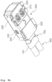
- FIGS. 6A to 6C are views of a connector assembly in which the plug connector 100 and the receptacle connector 200 are coupled to each other.
- FIG. 6A is a view of the connector assembly in which the plug connector 100 and the receptacle connector 200 are coupled to each other, when viewed from the upper rear side
- FIG. 6B is a view of the connector assembly in which the plug connector 100 and the receptacle connector 200 are coupled to each other, when viewed from the lower rear side
- FIG. 6C is a cross-sectional view of the connector assembly in which the plug connector 100 and the receptacle connector 200 are coupled to each other.
- the lower surface of the clip pin 210 is in electrical contact with the signal pad (not shown) of the circuit board P through elastic contact or soldering.
- the lower surface 112a of the second portion 112 of the signal pin 110 is in elastic contact with the upper portion of the clip pin 210.
- the signal line 310, the outer conductor 330, and the signal pin 110 are primarily shielded by the shield cans 120 and 130, secondary shielded by the plug shell 150, and tertiari shielded by the receptacle base 220 and the receptacle shell 240.
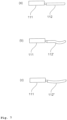
- FIG. 7 illustrates modifications of the signal pin 110.
- the second portion of the signal pin 110 may be modified in various forms.
- a second portion 112 of the signal pin 110 may be formed in a straight line, as shown in (a).
- a second portion 112' may be formed to be bent partially downward, as shown in (b), or a second portion 112" may be formed to be bent downward as a whole, as shown in (c).
- FIG. 8 illustrates modifications of the first insulating member 140.
- the first section of the first insulating member 140 may be modified in various forms.
- a first section 142 of the first insulating member 140 may be formed in a generally rectangular shape when viewed from above, as shown in (a).
- a first section 142' may be formed such that the front and rear sides thereof are scooped as shown in (b), or a first section 142" may be formed such that the front and rear sides thereof are angularly recessed.
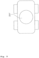
- FIG. 9 illustrates a modification of the second insulating member 230.
- the through hole of the second insulating member 230 may be modified in various forms.
- the through hole 231 of the second insulating member 230 may have a generally rectangular shape, or a through hole 231' may have a circular shape as shown in FIG. 9 .
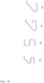
- FIG. 10 illustrates modifications of the clip pin 210.
- the shape of the clip 210 is not limited to the shape as shown in (a), such that the shape of the clip pin 210 may be modified in various forms, such as those shown in (b), (c), and (d), in which the lower surface of the clip pin 210 is in contact with the signal pad of the circuit board P and the upper portion of the clip pin 210 is in elastic contact with the lower surface 112a of the signal pin 110.
- the plug connector according to the embodiment of the present invention has a structure that is slidably inserted into the receptacle connector, which allows the height of the connector assembly to be minimized and makes a fastening copper wire of the plug connector parallel to the circuit board, thereby advantageous in miniaturization of the connector assembly.
- the plug connector according to the embodiment of the present invention has excellent electromagnetic wave shielding performance and is capable of simultaneous connecting a plurality of cables and a circuit board.
Landscapes
- Details Of Connecting Devices For Male And Female Coupling (AREA)
- Coupling Device And Connection With Printed Circuit (AREA)
Description
- The following description relates to a connector, and more particularly, to a plug connector that is slidably inserted into a receptacle connector.
- In various types of electronic devices (e.g. wired/wireless communication devices, etc.), internal circuits are implemented on circuit boards. A connector assembly including a receptacle connector and a plug connector is used to connect the circuit board to another electronic device or another circuit board. The receptacle connector is mounted on the circuit board, the plug connector is coupled to a cable, and the plug connector is coupled to the receptacle connector, so that the cable and the circuit board are electrically connected.
- Conventional connector assemblies have a structure in which a plug connector is vertically fastened to a receptacle connector with respect to a circuit board. Accordingly, it is difficult to miniaturize the connector assembly due to the height of the connector assembly and fastening copper wires of the plug connector, and such a structure is unfavorable in shielding electromagnetic waves. Also, it is difficult to simultaneous connect a plurality of cables and a circuit board with a single connector assembly.
-
EP 0 833 405 A1 discloses a plug connector that is slidably inserted into a receptacle connector. A signal pin of the plug connector has one side in electrical contact with one side of a a cable's signal line. A shield can is electrically spaced apart from the signal pin and surrounds the signal pin such that a lower surface of the other side of the signal pin is exposed. Furthermore, a first insulating member is coupled to the signal pin to insulate the signal pin and the shield can from each other. Finally, a plug shell is shown that surrounds the shield can such that the lower surface of the other side of the signal pin is exposed. -
US 2012/264337 A1 discloses an assembly which is formed by an electrical wire a plug housing. - An objective of the present invention is to provide a structure in which a plug connector is slidably inserted into a receptacle connector, which is favorable for miniaturization of a connector assembly by allowing the height of the connector assembly to be reduced and making a fastening copper wire of the plug connector parallel to a circuit board.
- In addition, another objective of the present invention is to provide a plug connector which provides excellent electromagnetic wave shielding performance and is capable of simultaneously connecting a plurality of cables and a circuit board.
- The objectives to be achieved by the present invention are not limited to the foregoing objectives, and additional objectives, which are not mentioned herein, will be readily understood by those skilled in the art from the following description.
- In one general aspect of the present invention, a plug connector configured to be slidably inserted into a receptacle connector includes: a signal pin having one side in electrical contact with one side of a signal line of a cable, a shield can electrically spaced apart from the signal pin and surrounding the signal pin such that a lower surface of the other side of the signal pin is exposed, a first insulating member coupled to the signal pin to insulate the signal pin and the shield can from each other, and a plug shell surrounding the shield can such that the lower surface of the other side of the signal pin is exposed.
- The shield can includes a lower shield can having a seating groove in which a lower portion of the cable is seated and an upper shield can having a seating groove in which an upper portion of the cable is seated and covering the lower shield can.
- A plurality of signal pins may be arranged in parallel to each other corresponding to a plurality of cables, and the shield can may include a shielding wall that shields between adjacent signal pins.
- The signal pin includes a first portion on one side thereof which has an insertion portion into which the signal line is inserted and a second portion on the other side thereof which is formed integrally with the first portion and has the lower surface of the other side.
- The first insulating member has a through hole through which the second portion of the signal pin passes, and may include a first section that forms an upper portion of the through hole and is formed to expose the lower surface of the other side of the second portion while covering an upper portion of the second portion; and a second section that forms a lower portion of the through hole and is formed below the first section to be shorter than the first section such that the lower surface of the other side of the second portion is exposed.
- According to the invention the shield includes a lower shield can having a seating groove in which a lower portion of the cable is seated and a seating groove in which the second section of the first insulating member is seated; and an upper shield can covering the lower shield can and having a seating groove in which an upper portion of the cable is seated and a seating groove in which the first section of the first insulating member is seated.
- The plug shell may be formed of a metal material.
- The plug shell may have an enclosing portion that encloses and supports a portion of the cable exposed to the outside of the shield can.
- Other features and aspects will be apparent from the following detailed description, the drawings, and the claims.
-
-
FIG. 1A is a perspective view of a connector assembly according to an embodiment of the present invention, when viewed from one side. -
FIG. 1B is a perspective view of the connector assembly ofFIG. 1A as viewed from another side. -
FIG. 1C is a perspective view of the connector assembly ofFIG. 1A as viewed from still another side. -
FIG. 2A is a first exploded view of a plug connector according to an embodiment of the present invention. -
FIG. 2B is a second exploded view of a plug connector according to an embodiment of the present invention. -
FIG. 2C is a view of the plug connector shown inFIG. 2B as viewed from a different side. -
FIG. 3A is a perspective view of a signal pin and a first insulating member of a plug connector according to an embodiment of the present invention. -
FIG. 3B is a view illustrating a state in which the signal pin and the first insulating member shown inFIG. 3A are separated from each other. -
FIG. 3C is a view of the signal pin and the first insulating member shown inFIG. 3B , when viewed from a different side. -
FIG. 4A is a first exploded view of a receptacle connector into which a plug connector according to an embodiment of the present invention is slidably inserted. -
FIG. 4B is a second exploded view of a receptacle connector into which a plug connector according to an embodiment of the present invention is slidably inserted. -
FIG. 4C is a view of the receptacle connector shown inFIG. 4B , when viewed from a different side. -
FIG. 5 is a view illustrating a state in which a clip pin and a second insulating member of a receptacle connector into which a plug connector according to an embodiment of the present invention is slidably inserted. -
FIG. 6A is a view of a connector assembly in which a plug connector and a receptacle connector are coupled to each other, when viewed from one side. -
FIG. 6B is a view of the connector assembly shown inFIG. 6A , when viewed from a different side. -
FIG. 6C is a cross-sectional view of a connector assembly in which a plug connector and a receptacle connector are coupled to each other. -
FIG. 7 illustrates modifications of a signal pin. -
FIG. 8 illustrates modifications of a first insulating member. -
FIG. 9 illustrates modifications of a second insulating member. -
FIG. 10 illustrates modifications of a shield pin. - Throughout the drawings and the detailed description, unless otherwise described, the same drawing reference numerals will be understood to refer to the same elements, features, and structures. The relative size and depiction of these elements may be exaggerated for clarity, illustration, and convenience.
-
FIGS. 1A to 1C are views of a connector assembly according to an embodiment of the present invention. In this specification, for convenience of description, with respect toFIG. 1A , the positive X-axis direction is defined as a forward direction (or a front side or a front end) and the negative X-axis direction is a rearward direction (or a rear side or a rear end). The positive Z-axis direction is defined as an upper direction (or an upper surface or an upper end) and the negative Z-axis direction is a lower direction (or a lower surface or a lower end). The positive and negative Y-axis directions are defined as a lateral direction.FIG. 1A is a perspective view of the connector assembly as viewed from the upper rear side thereof,FIG. 1B is a perspective view of the connector assembly as viewed from the lower rear side thereof andFIG. 1C is a perspective view of the connector assembly as viewed from the upper front side thereof. - The connector assembly according to the present embodiment includes a
receptacle connector 200 mounted on a circuit board (which is designated by reference P inFIG. 6C ), and aplug connector 100 to be coupled to acable 300 and slidably inserted into thereceptacle connector 200. - The
receptacle connector 200 may be mounted on the circuit board P using a surface mount method, such as surface mount device (SMD) or surface mount technology (SMT), a through-hole method, such as single in-line package (SIP), dual in-line package (DIP), quad in-line package (QIP), or the like, or both the surface mount method and the through-hole method. According to an embodiment, thereceptacle connector 200 may not be a separate component but may be integrally formed with the circuit board P. - The
receptacle connector 200 may have a shape in which the front end is open and the rear end is closed so that theplug connector 100 can be slidably inserted from the front end. -
FIGS. 2A to 2C are views of theplug connector 100 according to an embodiment of the present invention.FIG. 2A is a first exploded view of theplug connector 100 as viewed from the upper rear side thereof,FIG. 2B is a second exploded view of theplug connector 100 as viewed from the upper rear side thereof, andFIG. 2C is a view of theplug connector 100 shown inFIG. 2B , when viewed from the lower rear side. - In the present embodiment, a coaxial cable is described as an example of the
cable 300 coupled to theplug connector 100, but thecable 300 may be any of various types of cables, such as a data cable, a wire, a flexible flat cable (FFC), a flexible printed circuit (FPC), and the like, instead of the coaxial cable. - The
cable 300 may include a signal line (internal conductor) 310, anouter conductor 330 made of aluminum, copper, etc. which shields electromagnetic waves of thesignal line 310, adielectric material 320 that insulates and separates thesignal line 310 and theouter conductor 330 from each other, and ajacket 340 that protects theouter conductor 330. - The
plug connector 100 includes signal pins 110,shield cans member 140, and aplug shell 150. - In the present embodiment, two
cables 300 are provided, but the number ofcables 300 may be one or three or more. When there is a plurality ofcables 300, thecables 300 are disposed in parallel to each other. Those skilled in the art will understand that the number or structures of the signal pins 110, theshield cans members 140, and theplug shells 150 may be appropriately modified according to the number ofcables 300. - The
signal pin 110 may be formed such that a front end thereof is in electrical contact with thesignal line 310 of thecable 300 and alower surface 112a of a rear side thereof is in elastic contact with an upper side of aclip pin 210 of thereceptacle connector 200 which will be described below. Thesignal pin 110 is provided for eachcable 300, and when there is a plurality ofcables 300, a plurality of signal pins 110 are also arranged in parallel to each other. - The
signal pin 110 includes afirst portion 111 at the front side and asecond portion 112 integrally formed at the rear side with thefirst portion 111. Thefirst portion 111 includes an insertion portion into which thesignal line 310 is inserted. Thefirst portion 111 of thesignal pin 110 and thesignal line 310 may be in electrical contact with each other by tightening or soldering. One or more protrusions may be formed inside thefirst portion 111 of thesignal pin 110 to improve tensile force for fixing thesignal line 310. Thesecond portion 112 has alower surface 112a in elastic contact with an upper portion of theclip pin 210 of thereceptacle connector 200. - The
shield cans signal pin 110 so that thelower surface 112a of thesecond portion 112 of thesignal pin 110 is exposed, and are formed to be electrically spaced apart from thesignal pin 110. Theshield cans shield cans seating groove 121 in which the lower portion of thecable 300 is seated. The upper shield can 130 is formed to cover the lower shield can 120 and has aseating groove 131 in which an upper portion of thecable 300 is seated. In the present embodiment, theshield cans shield cans - The lower shield can 120 may include a
shielding wall 122 that shields between adjacent signal pins 110. In addition, the upper shield can 130 may include ahole 132 into which an upper portion of the shieldingwall 122 is inserted. According to an embodiment, the shielding wall that shields between adjacent signal pins 110 may be provided on the upper shield can 130 instead of the lower shield can 120. - The first insulating
member 140 is coupled to the rear side of thesignal pin 110, specifically, thesecond portion 112 of thesignal pin 110, to insulate thesignal pin 110 from theshield cans FIGS. 3A to 3C are views specifically illustrating the signal pins 110 and the first insulatingmember 140.FIG. 3A is a view of the signal pins 110 and the first insulatingmember 140, when viewed from the lower rear side,FIG. 3B is a view illustrating a state in which the signal pins 110 and the first insulatingmember 140 are separated from each other, andFIG. 3C is a view illustrating the signal pins 110 and the first insulatingmember 140 shown inFIG. 3B , when viewed from the upper front side. - The first insulating
member 140 has a throughhole 141 through which thesecond portion 112 of thesignal pin 110 passes, and consists of afirst section 142 and asecond section 143 that may be integrally formed with thefirst section 142. The throughhole 141, thefirst section 142, and thesecond section 143 are provided for eachsignal pin 110. Thefirst section 142 forms an upper portion of the throughhole 141 and is elongated along a length direction of thesecond portion 112 such that it covers an upper portion of thesecond portion 112 of thesignal pin 110 and exposes thelower surface 112a of thesecond portion 112. Thesecond section 143 forms a lower portion of the throughhole 141 and is formed below thefirst section 142 to be shorter than thefirst section 142 along the length direction of thesecond portion 112 such that thelower surface 112a of thesecond portion 112 of thesignal pin 110 is exposed. - The lower shield can 120 has a
seating groove 123 in which thesecond section 143 of the first insulatingmember 140 is seated. In addition, the upper shield can 130 includes aseating groove 133 in which thefirst section 142 of the first insulatingmember 140 is seated. - The
plug shell 150 surrounds the upper, lower, and both lateral surfaces of theshield cans 120 and 130 (specifically, the upper surface and both lateral surfaces of the upper shield can 130 and the lower surface and both lateral surfaces of the lower shield can 120) such that thelower surface 112a of thesecond portion 112 of thesignal pin 110 is exposed. - The
plug shell 150 may be formed of a metal material for shielding electromagnetic waves. Also, theplug shell 150 may include an enclosing portion that encloses and supports a part of thecable 300 exposed to the outside of theshield cans shield cans portion 151 may extend in the front direction from the lower portion of theplug shell 150. The enclosingportion 151 may prevent damage due to excessive bending or separation of thecable 300. - According to the
plug connector 100 in accordance with an embodiment of the present invention, electromagnetic waves generated through thesignal line 310 and theouter conductor 330 of thecable 300 and thesignal pin 110 are primarily shielded by theshield cans plug shell 150, thus improving electromagnetic wave shielding performance. In addition, since electromagnetic waves betweenadjacent signal lines 310 or between adjacent signal pins 110 are shielded by the shieldingwalls 122 in theshield cans -
FIGS. 4A to 4C are views of areceptacle connector 200 into which aplug connector 100 according to an embodiment of the present invention is slidably inserted.FIG. 4A is a first exploded view of thereceptacle connector 200 viewed from the upper front side thereof,FIG. 4B is a second exploded view of thereceptacle connector 200 viewed from the upper front side thereof, andFIG. 4C is a view of thereceptacle connector 200 shown inFIG. 4B when viewed from the lower front side. - The
receptacle connector 200 includes aclip pin 210, areceptacle base 220, a second insulatingmember 230, and areceptacle shell 240. - The
clip pin 210 may be formed such that a lower surface thereof is in electrical contact with a signal pad (not shown) of a circuit board (which is designated by reference P inFIG. 6c ) through elastic contact or soldering and an upper portion thereof is in elastic contact with thelower surface 112a of thesecond portion 112 of thesignal pin 110. - The electrical contact of the
clip pin 210 may be made by a surface mount method, such as SMD o r SMT, a through-hole method, such as SIP, DIP, and QIP, or the like. When there are a plurality of signal pins 110, a plurality of clip pins 210 are also provided for eachsignal pin 110 and are arranged according to the arrangement of the signal pins 110. - The
receptacle base 220 is installed on an upper surface of the substrate P, and provides aspace 221 in which the second insulatingmember 230 and theclip pin 210 are accommodated. Thespace 221 may be formed to penetrate the top and bottom of thereceptacle base 220. - The second insulating
member 230 is inserted into thespace 221 of thereceptacle base 220 and surrounds theclip pin 210 from the side to fix the clip pin 2 1 0 and simultaneously insulate theclip pin 210 from thereceptacle base 220. - The
receptacle shell 240 covers thereceptacle base 220 and provides a space in which theplug connector 100 is slidably inserted together with thereceptacle base 220. That is, theplug connector 100 is slidably inserted into the space defined by anupper surface 220a of thereceptacle base 220 and an inner upper surface and both inner lateral surfaces of thereceptacle shell 240. - The
receptacle base 220 and thereceptacle shell 240 may be formed of a metal material to shield electromagnetic waves. In a state in which theplug connector 100 is coupled to thereceptacle connector 200, electromagnetic waves generated through thesignal line 310, theouter conductor 330, and thesignal pin 110 are primarily shielded by theshield cans plug shell 150, and tertiarily shielded by thereceptacle base 220 and thereceptacle Shell 240. - For a firm coupling between the
plug connector 100 and thereceptacle connector 200, theplug shell 150 may have afastening hole 152 on the upper surface, and thereceptacle shell 240 may have anelastic fastening portion 241 on the upper surface, which is inserted and fastened into thefastening hole 152. In addition, thereceptacle shell 240 may include fastening holes 242 on both sides thereof, and theplug shell 150 may includefastening protrusions 153 on both sides thereof, which are inserted and fastened into the fastening holes 242. In addition, theplug shell 150 may haveprotrusions 154 on both sides thereof, and theprojections 154 are in close contact with both inner sides of thereceptacle shell 240. Also, theplug shell 150 has a plurality of protrusions 155 (for example, at four points on front, rear, and both sides) on a lower surface 50a thereof, and theprotrusions 155 are in close contact with theupper surface 220a of thereceptacle base 220. -
FIG. 5 is a view illustrating a state in which theclip pin 210 and the second insulatingmember 230 of thereceptacle connector 200 are separated from each other. - The
clip pin 210 may include afirst section 211 having a lower surface in contact with the signal pad of the circuit board P, asecond section 212 extending substantially upward from a front end of thefirst section 211, athird section 213 extending substantially rearward from an upper end of thesecond section 212, afourth section 214 extending obliquely forward and upward from a rear end of thethird section 213, and afifth section 215 extending obliquely forward and downward from an upper end of thefourth section 214. A lower surface of thefirst section 211 may be in elastic contact with the signal pad of the circuit board P, and an upper portion of theclip pin 210, that is, a portion between thefourth section 214 and thefifth section 215, may be in elastic contact with thelower surface 112a of thesecond portion 112 of thesignal pin 110. The electrical contact of the lower surface of thefirst section 211 of theclip pin 210 may be made by a surface mount method, such as SMD or SMT, a through-hole method, such as SIP, DIP, and QIP, or the like. In the present example, theclip pin 210 is disposed so that thefifth section 215 faces forward, but theclip pin 210 may be disposed so that thefifth section 214 faces rearward. - The second insulating
member 230 may have a throughhole 231 penetrating vertically to accommodate theclip pin 210. In addition, the second insulatingmember 230 may haveholes 232 on both sides, and theclip pin 210 may haveprotrusions 216 extending from thethird section 213 on both sides. Theprotrusions 216 are inserted into thehole 232 to fix theclip pin 210 to the second insulatingmember 230. The second insulatingmember 230 may haveprotrusions 233 on both sides, and receivinggrooves 222 to accommodate theprotrusions 233 may be formed on both sides of thespace 221 into which the second insulatingmember 230 of thereceptacle base 220 is inserted -
FIGS. 6A to 6C are views of a connector assembly in which theplug connector 100 and thereceptacle connector 200 are coupled to each other.FIG. 6A is a view of the connector assembly in which theplug connector 100 and thereceptacle connector 200 are coupled to each other, when viewed from the upper rear side,FIG. 6B is a view of the connector assembly in which theplug connector 100 and thereceptacle connector 200 are coupled to each other, when viewed from the lower rear side, andFIG. 6C is a cross-sectional view of the connector assembly in which theplug connector 100 and thereceptacle connector 200 are coupled to each other. - Referring to
FIG. 6C , the lower surface of theclip pin 210 is in electrical contact with the signal pad (not shown) of the circuit board P through elastic contact or soldering. Thelower surface 112a of thesecond portion 112 of thesignal pin 110 is in elastic contact with the upper portion of theclip pin 210. In addition, thesignal line 310, theouter conductor 330, and thesignal pin 110 are primarily shielded by theshield cans plug shell 150, and tertiari shielded by thereceptacle base 220 and thereceptacle shell 240. -
FIG. 7 illustrates modifications of thesignal pin 110. The second portion of thesignal pin 110 may be modified in various forms. For example, asecond portion 112 of thesignal pin 110 may be formed in a straight line, as shown in (a). Alternatively, a second portion 112' may be formed to be bent partially downward, as shown in (b), or asecond portion 112" may be formed to be bent downward as a whole, as shown in (c). -
FIG. 8 illustrates modifications of the first insulatingmember 140. The first section of the first insulatingmember 140 may be modified in various forms. For example, afirst section 142 of the first insulatingmember 140 may be formed in a generally rectangular shape when viewed from above, as shown in (a). Alternatively, a first section 142' may be formed such that the front and rear sides thereof are scooped as shown in (b), or afirst section 142" may be formed such that the front and rear sides thereof are angularly recessed. -
FIG. 9 illustrates a modification of the second insulatingmember 230. The through hole of the second insulatingmember 230 may be modified in various forms. For example, as shown inFIG. 5 , the throughhole 231 of the second insulatingmember 230 may have a generally rectangular shape, or a through hole 231' may have a circular shape as shown inFIG. 9 . -
FIG. 10 illustrates modifications of theclip pin 210. In the present example, the shape of theclip 210 is not limited to the shape as shown in (a), such that the shape of theclip pin 210 may be modified in various forms, such as those shown in (b), (c), and (d), in which the lower surface of theclip pin 210 is in contact with the signal pad of the circuit board P and the upper portion of theclip pin 210 is in elastic contact with thelower surface 112a of thesignal pin 110. - The plug connector according to the embodiment of the present invention has a structure that is slidably inserted into the receptacle connector, which allows the height of the connector assembly to be minimized and makes a fastening copper wire of the plug connector parallel to the circuit board, thereby advantageous in miniaturization of the connector assembly.
- In addition, the plug connector according to the embodiment of the present invention has excellent electromagnetic wave shielding performance and is capable of simultaneous connecting a plurality of cables and a circuit board.
- The effects of the present invention are not limited to those mentioned above, and unmentioned other effects may be clearly understood by those skilled in the art from the above descriptions.
- A number of examples have been described above. Nevertheless, it will be understood that various modifications may be made. For example, suitable results may be achieved if the described techniques are performed in a different order and/or if components in a described system, architecture, device, or circuit are combined in a different manner and/or replaced or supplemented by other components or their equivalents. Accordingly, other implementations are within the scope of the following claims.
Claims (4)
- A plug connector (100) configured to be slidably inserted into a receptacle connector (200), comprising:- a signal pin (110) having one side in electrical contact with one side of a signal line (310) of a cable (300),- a shield can (120, 130) electrically spaced apart from the signal pin (110) and surrounding the signal pin (110) such that a lower surface (112a) of the other side of the signal pin (110) is exposed;- a first insulating member (140) coupled to the signal pin (110) to insulate the signal pin (110) and the shield can (120, 130) from each other; and- a plug shell (150) surrounding the shield can (120, 130) such that the lower surface (112a) of the other side of the signal pin (110) is exposed,wherein the signal pin (110) comprises a first portion on one side thereof which has an insertion portion into which the signal line (310) is inserted and a second portion on the other side thereof which is formed integrally with the first portion and has the lower surface (112a) of the other side of the signal pin (110),wherein the first insulating member (140) has a through hole (141) through which the second portion of the signal pin (110) passes, and comprises a first section (142) that forms an upper portion of the through hole (141) and is formed to expose the lower surface (112a) of the other side of the second portion while covering an upper portion of the second portion; and a second section (143) that forms a lower portion of the through hole (141) and is formed below the first section (142) to be shorter than the first section (142) such that the lower surface (112a) of the other side of the second portion is exposed,- wherein the shield can (120, 130) comprises: a lower shield can (120) having a seating groove (121) in which a lower portion of the cable (300) is seated and a seating groove (123) in which the second section (143) of the first insulating member (140) is seated; and an upper shield can (130) covering the lower shield can (120) and having a seating groove (131) in which an upper portion of the cable (300) is seated and a seating groove (133) in which the first section (142) of the first insulating member (140) is seated.
- The plug connector (1 00) of claim 1, wherein a plurality of signal pins (110) are arranged in parallel to each other corresponding to a plurality of cables (300) and the shield can (120, 130) comprises a shielding wall that shields between adjacent signal pins (110).
- The plug connector (100) of claim 1, wherein the plug shell (150) is formed of a metal material.
- The plug connector (100) of claim 1, wherein the plug shell (150) has an enclosing portion that encloses and supports a portion of the cable (300) exposed to the outside of the shield can (120, 130).
Applications Claiming Priority (1)
| Application Number | Priority Date | Filing Date | Title |
|---|---|---|---|
| KR1020200062338A KR102348969B1 (en) | 2020-05-25 | 2020-05-25 | Plug connector slidingly inserted into receptacle connector |
Publications (2)
| Publication Number | Publication Date |
|---|---|
| EP3916931A1 EP3916931A1 (en) | 2021-12-01 |
| EP3916931B1 true EP3916931B1 (en) | 2023-06-28 |
Family
ID=76011794
Family Applications (1)
| Application Number | Title | Priority Date | Filing Date |
|---|---|---|---|
| EP21174678.9A Active EP3916931B1 (en) | 2020-05-25 | 2021-05-19 | Plug connector slidably inserted into receptacle connector |
Country Status (6)
| Country | Link |
|---|---|
| US (1) | US11469552B2 (en) |
| EP (1) | EP3916931B1 (en) |
| JP (1) | JP7113551B2 (en) |
| KR (1) | KR102348969B1 (en) |
| CN (1) | CN113725664B (en) |
| TW (1) | TWI799863B (en) |
Families Citing this family (5)
| Publication number | Priority date | Publication date | Assignee | Title |
|---|---|---|---|---|
| CN116250152A (en) | 2020-09-24 | 2023-06-09 | 京瓷Avx元器件公司 | Solderless Wire-to-Board Single Pair Ethernet Connection System |
| US11757231B2 (en) * | 2020-10-07 | 2023-09-12 | Dell Products L.P. | Two-stage connector with internal terminal correction and repair |
| KR20240049371A (en) * | 2021-09-01 | 2024-04-16 | 에프씨아이 유에스에이 엘엘씨 | High-speed, robust connector |
| CN117981175A (en) | 2021-09-23 | 2024-05-03 | 京瓷Avx元器件公司 | Wire-to-wire tandem connector |
| JP2024015847A (en) * | 2022-07-25 | 2024-02-06 | 日本航空電子工業株式会社 | connector with board |
Family Cites Families (10)
| Publication number | Priority date | Publication date | Assignee | Title |
|---|---|---|---|---|
| EP0833405A1 (en) * | 1996-09-28 | 1998-04-01 | Harting KGaA | Plug connection for coaxial cables |
| AU9385998A (en) * | 1998-01-15 | 1999-08-02 | Siemon Company, The | Enhanced performance telecommunications connector |
| US7156678B2 (en) * | 2005-04-07 | 2007-01-02 | 3M Innovative Properties Company | Printed circuit connector assembly |
| US8096833B2 (en) * | 2010-01-15 | 2012-01-17 | Tyco Electronics Corporation | Plug assembly |
| US8608512B2 (en) * | 2011-04-18 | 2013-12-17 | Fci Americas Technology, Llc | Cable connector |
| CN102957054A (en) * | 2011-08-25 | 2013-03-06 | 鸿富锦精密工业(深圳)有限公司 | USB (universal serial bus) connector and connecting device with same |
| CN202308430U (en) * | 2011-11-07 | 2012-07-04 | 昆山联滔电子有限公司 | Plug connector |
| CN110190461B (en) * | 2014-11-07 | 2020-07-28 | 富士康(昆山)电脑接插件有限公司 | Plug connector |
| JP6729274B2 (en) * | 2016-10-12 | 2020-07-22 | 株式会社オートネットワーク技術研究所 | Connector structure |
| EP3735719B1 (en) * | 2018-01-05 | 2024-06-12 | Molex, LLC | Low profile electrical connector system with differential pair cable interface |
-
2020
- 2020-05-25 KR KR1020200062338A patent/KR102348969B1/en active Active
-
2021
- 2021-05-12 US US17/318,082 patent/US11469552B2/en active Active
- 2021-05-14 JP JP2021082116A patent/JP7113551B2/en active Active
- 2021-05-19 TW TW110118035A patent/TWI799863B/en active
- 2021-05-19 EP EP21174678.9A patent/EP3916931B1/en active Active
- 2021-05-24 CN CN202110566121.2A patent/CN113725664B/en active Active
Also Published As
| Publication number | Publication date |
|---|---|
| TWI799863B (en) | 2023-04-21 |
| JP7113551B2 (en) | 2022-08-05 |
| CN113725664B (en) | 2024-08-02 |
| KR102348969B1 (en) | 2022-01-10 |
| US11469552B2 (en) | 2022-10-11 |
| KR20210145445A (en) | 2021-12-02 |
| EP3916931A1 (en) | 2021-12-01 |
| US20210367382A1 (en) | 2021-11-25 |
| JP2021190423A (en) | 2021-12-13 |
| TW202145654A (en) | 2021-12-01 |
| CN113725664A (en) | 2021-11-30 |
Similar Documents
| Publication | Publication Date | Title |
|---|---|---|
| US11469552B2 (en) | Plug connector slidably inserted into receptacle connector | |
| US11196203B1 (en) | Connector assembly including receptacle connector and plug connector | |
| TWI769682B (en) | Electrical connector with electromagnetic shielding function | |
| EP3751672A1 (en) | Compact coaxial cable connector for transmitting super high frequency signals | |
| US10833461B2 (en) | Connectors for coaxial cables | |
| KR101125067B1 (en) | Connector for coaxial cable | |
| KR101344933B1 (en) | Connector assembly | |
| US20240291207A1 (en) | Connector assembly comprising receptacle connector and plug connector, and plug connector | |
| KR102311610B1 (en) | Small coaxial cable connector for transmitting super high frequency signal | |
| US12597740B2 (en) | Connector assembly including receptacle connector and plug connector, and plug connector | |
| JP2002367735A (en) | Shielded cable connector and electronic equipment | |
| US7854626B2 (en) | Connection structure for small diameter shielded cable | |
| US20240347982A1 (en) | Cable card assembly of an electrical connector having capacitors | |
| JP2007317554A (en) | Connector and connector system |
Legal Events
| Date | Code | Title | Description |
|---|---|---|---|
| PUAI | Public reference made under article 153(3) epc to a published international application that has entered the european phase |
Free format text: ORIGINAL CODE: 0009012 |
|
| STAA | Information on the status of an ep patent application or granted ep patent |
Free format text: STATUS: REQUEST FOR EXAMINATION WAS MADE |
|
| 17P | Request for examination filed |
Effective date: 20210519 |
|
| AK | Designated contracting states |
Kind code of ref document: A1 Designated state(s): AL AT BE BG CH CY CZ DE DK EE ES FI FR GB GR HR HU IE IS IT LI LT LU LV MC MK MT NL NO PL PT RO RS SE SI SK SM TR |
|
| B565 | Issuance of search results under rule 164(2) epc |
Effective date: 20211020 |
|
| RAP3 | Party data changed (applicant data changed or rights of an application transferred) |
Owner name: SENSORVIEW CO., LTD. |
|
| GRAP | Despatch of communication of intention to grant a patent |
Free format text: ORIGINAL CODE: EPIDOSNIGR1 |
|
| STAA | Information on the status of an ep patent application or granted ep patent |
Free format text: STATUS: GRANT OF PATENT IS INTENDED |
|
| RIC1 | Information provided on ipc code assigned before grant |
Ipc: H01R 103/00 20060101ALN20221122BHEP Ipc: H01R 24/64 20110101ALN20221122BHEP Ipc: H01R 12/75 20110101ALN20221122BHEP Ipc: H01R 9/05 20060101ALI20221122BHEP Ipc: H01R 13/6589 20110101AFI20221122BHEP |
|
| INTG | Intention to grant announced |
Effective date: 20221208 |
|
| GRAS | Grant fee paid |
Free format text: ORIGINAL CODE: EPIDOSNIGR3 |
|
| GRAA | (expected) grant |
Free format text: ORIGINAL CODE: 0009210 |
|
| STAA | Information on the status of an ep patent application or granted ep patent |
Free format text: STATUS: THE PATENT HAS BEEN GRANTED |
|
| AK | Designated contracting states |
Kind code of ref document: B1 Designated state(s): AL AT BE BG CH CY CZ DE DK EE ES FI FR GB GR HR HU IE IS IT LI LT LU LV MC MK MT NL NO PL PT RO RS SE SI SK SM TR |
|
| REG | Reference to a national code |
Ref country code: CH Ref legal event code: EP |
|
| REG | Reference to a national code |
Ref country code: AT Ref legal event code: REF Ref document number: 1583585 Country of ref document: AT Kind code of ref document: T Effective date: 20230715 |
|
| REG | Reference to a national code |
Ref country code: IE Ref legal event code: FG4D |
|
| REG | Reference to a national code |
Ref country code: DE Ref legal event code: R096 Ref document number: 602021003102 Country of ref document: DE |
|
| REG | Reference to a national code |
Ref country code: LT Ref legal event code: MG9D |
|
| PG25 | Lapsed in a contracting state [announced via postgrant information from national office to epo] |
Ref country code: SE Free format text: LAPSE BECAUSE OF FAILURE TO SUBMIT A TRANSLATION OF THE DESCRIPTION OR TO PAY THE FEE WITHIN THE PRESCRIBED TIME-LIMIT Effective date: 20230628 Ref country code: NO Free format text: LAPSE BECAUSE OF FAILURE TO SUBMIT A TRANSLATION OF THE DESCRIPTION OR TO PAY THE FEE WITHIN THE PRESCRIBED TIME-LIMIT Effective date: 20230928 |
|
| REG | Reference to a national code |
Ref country code: NL Ref legal event code: MP Effective date: 20230628 |
|
| REG | Reference to a national code |
Ref country code: AT Ref legal event code: MK05 Ref document number: 1583585 Country of ref document: AT Kind code of ref document: T Effective date: 20230628 |
|
| PG25 | Lapsed in a contracting state [announced via postgrant information from national office to epo] |
Ref country code: RS Free format text: LAPSE BECAUSE OF FAILURE TO SUBMIT A TRANSLATION OF THE DESCRIPTION OR TO PAY THE FEE WITHIN THE PRESCRIBED TIME-LIMIT Effective date: 20230628 Ref country code: NL Free format text: LAPSE BECAUSE OF FAILURE TO SUBMIT A TRANSLATION OF THE DESCRIPTION OR TO PAY THE FEE WITHIN THE PRESCRIBED TIME-LIMIT Effective date: 20230628 Ref country code: LV Free format text: LAPSE BECAUSE OF FAILURE TO SUBMIT A TRANSLATION OF THE DESCRIPTION OR TO PAY THE FEE WITHIN THE PRESCRIBED TIME-LIMIT Effective date: 20230628 Ref country code: LT Free format text: LAPSE BECAUSE OF FAILURE TO SUBMIT A TRANSLATION OF THE DESCRIPTION OR TO PAY THE FEE WITHIN THE PRESCRIBED TIME-LIMIT Effective date: 20230628 Ref country code: HR Free format text: LAPSE BECAUSE OF FAILURE TO SUBMIT A TRANSLATION OF THE DESCRIPTION OR TO PAY THE FEE WITHIN THE PRESCRIBED TIME-LIMIT Effective date: 20230628 Ref country code: GR Free format text: LAPSE BECAUSE OF FAILURE TO SUBMIT A TRANSLATION OF THE DESCRIPTION OR TO PAY THE FEE WITHIN THE PRESCRIBED TIME-LIMIT Effective date: 20230929 |
|
| PG25 | Lapsed in a contracting state [announced via postgrant information from national office to epo] |
Ref country code: FI Free format text: LAPSE BECAUSE OF FAILURE TO SUBMIT A TRANSLATION OF THE DESCRIPTION OR TO PAY THE FEE WITHIN THE PRESCRIBED TIME-LIMIT Effective date: 20230628 |
|
| PG25 | Lapsed in a contracting state [announced via postgrant information from national office to epo] |
Ref country code: SK Free format text: LAPSE BECAUSE OF FAILURE TO SUBMIT A TRANSLATION OF THE DESCRIPTION OR TO PAY THE FEE WITHIN THE PRESCRIBED TIME-LIMIT Effective date: 20230628 |
|
| PG25 | Lapsed in a contracting state [announced via postgrant information from national office to epo] |
Ref country code: ES Free format text: LAPSE BECAUSE OF FAILURE TO SUBMIT A TRANSLATION OF THE DESCRIPTION OR TO PAY THE FEE WITHIN THE PRESCRIBED TIME-LIMIT Effective date: 20230628 |
|
| PG25 | Lapsed in a contracting state [announced via postgrant information from national office to epo] |
Ref country code: IS Free format text: LAPSE BECAUSE OF FAILURE TO SUBMIT A TRANSLATION OF THE DESCRIPTION OR TO PAY THE FEE WITHIN THE PRESCRIBED TIME-LIMIT Effective date: 20231028 |
|
| PG25 | Lapsed in a contracting state [announced via postgrant information from national office to epo] |
Ref country code: SM Free format text: LAPSE BECAUSE OF FAILURE TO SUBMIT A TRANSLATION OF THE DESCRIPTION OR TO PAY THE FEE WITHIN THE PRESCRIBED TIME-LIMIT Effective date: 20230628 Ref country code: SK Free format text: LAPSE BECAUSE OF FAILURE TO SUBMIT A TRANSLATION OF THE DESCRIPTION OR TO PAY THE FEE WITHIN THE PRESCRIBED TIME-LIMIT Effective date: 20230628 Ref country code: RO Free format text: LAPSE BECAUSE OF FAILURE TO SUBMIT A TRANSLATION OF THE DESCRIPTION OR TO PAY THE FEE WITHIN THE PRESCRIBED TIME-LIMIT Effective date: 20230628 Ref country code: PT Free format text: LAPSE BECAUSE OF FAILURE TO SUBMIT A TRANSLATION OF THE DESCRIPTION OR TO PAY THE FEE WITHIN THE PRESCRIBED TIME-LIMIT Effective date: 20231030 Ref country code: IS Free format text: LAPSE BECAUSE OF FAILURE TO SUBMIT A TRANSLATION OF THE DESCRIPTION OR TO PAY THE FEE WITHIN THE PRESCRIBED TIME-LIMIT Effective date: 20231028 Ref country code: ES Free format text: LAPSE BECAUSE OF FAILURE TO SUBMIT A TRANSLATION OF THE DESCRIPTION OR TO PAY THE FEE WITHIN THE PRESCRIBED TIME-LIMIT Effective date: 20230628 Ref country code: EE Free format text: LAPSE BECAUSE OF FAILURE TO SUBMIT A TRANSLATION OF THE DESCRIPTION OR TO PAY THE FEE WITHIN THE PRESCRIBED TIME-LIMIT Effective date: 20230628 Ref country code: CZ Free format text: LAPSE BECAUSE OF FAILURE TO SUBMIT A TRANSLATION OF THE DESCRIPTION OR TO PAY THE FEE WITHIN THE PRESCRIBED TIME-LIMIT Effective date: 20230628 Ref country code: AT Free format text: LAPSE BECAUSE OF FAILURE TO SUBMIT A TRANSLATION OF THE DESCRIPTION OR TO PAY THE FEE WITHIN THE PRESCRIBED TIME-LIMIT Effective date: 20230628 |
|
| PG25 | Lapsed in a contracting state [announced via postgrant information from national office to epo] |
Ref country code: PL Free format text: LAPSE BECAUSE OF FAILURE TO SUBMIT A TRANSLATION OF THE DESCRIPTION OR TO PAY THE FEE WITHIN THE PRESCRIBED TIME-LIMIT Effective date: 20230628 |
|
| REG | Reference to a national code |
Ref country code: DE Ref legal event code: R097 Ref document number: 602021003102 Country of ref document: DE |
|
| PG25 | Lapsed in a contracting state [announced via postgrant information from national office to epo] |
Ref country code: DK Free format text: LAPSE BECAUSE OF FAILURE TO SUBMIT A TRANSLATION OF THE DESCRIPTION OR TO PAY THE FEE WITHIN THE PRESCRIBED TIME-LIMIT Effective date: 20230628 |
|
| PLBE | No opposition filed within time limit |
Free format text: ORIGINAL CODE: 0009261 |
|
| STAA | Information on the status of an ep patent application or granted ep patent |
Free format text: STATUS: NO OPPOSITION FILED WITHIN TIME LIMIT |
|
| PG25 | Lapsed in a contracting state [announced via postgrant information from national office to epo] |
Ref country code: IT Free format text: LAPSE BECAUSE OF FAILURE TO SUBMIT A TRANSLATION OF THE DESCRIPTION OR TO PAY THE FEE WITHIN THE PRESCRIBED TIME-LIMIT Effective date: 20230628 |
|
| 26N | No opposition filed |
Effective date: 20240402 |
|
| PG25 | Lapsed in a contracting state [announced via postgrant information from national office to epo] |
Ref country code: SI Free format text: LAPSE BECAUSE OF FAILURE TO SUBMIT A TRANSLATION OF THE DESCRIPTION OR TO PAY THE FEE WITHIN THE PRESCRIBED TIME-LIMIT Effective date: 20230628 |
|
| PG25 | Lapsed in a contracting state [announced via postgrant information from national office to epo] |
Ref country code: BG Free format text: LAPSE BECAUSE OF FAILURE TO SUBMIT A TRANSLATION OF THE DESCRIPTION OR TO PAY THE FEE WITHIN THE PRESCRIBED TIME-LIMIT Effective date: 20230628 |
|
| PG25 | Lapsed in a contracting state [announced via postgrant information from national office to epo] |
Ref country code: BG Free format text: LAPSE BECAUSE OF FAILURE TO SUBMIT A TRANSLATION OF THE DESCRIPTION OR TO PAY THE FEE WITHIN THE PRESCRIBED TIME-LIMIT Effective date: 20230628 |
|
| PG25 | Lapsed in a contracting state [announced via postgrant information from national office to epo] |
Ref country code: MC Free format text: LAPSE BECAUSE OF FAILURE TO SUBMIT A TRANSLATION OF THE DESCRIPTION OR TO PAY THE FEE WITHIN THE PRESCRIBED TIME-LIMIT Effective date: 20230628 |
|
| PG25 | Lapsed in a contracting state [announced via postgrant information from national office to epo] |
Ref country code: LU Free format text: LAPSE BECAUSE OF NON-PAYMENT OF DUE FEES Effective date: 20240519 |
|
| PG25 | Lapsed in a contracting state [announced via postgrant information from national office to epo] |
Ref country code: MC Free format text: LAPSE BECAUSE OF FAILURE TO SUBMIT A TRANSLATION OF THE DESCRIPTION OR TO PAY THE FEE WITHIN THE PRESCRIBED TIME-LIMIT Effective date: 20230628 Ref country code: LU Free format text: LAPSE BECAUSE OF NON-PAYMENT OF DUE FEES Effective date: 20240519 |
|
| REG | Reference to a national code |
Ref country code: BE Ref legal event code: MM Effective date: 20240531 |
|
| PG25 | Lapsed in a contracting state [announced via postgrant information from national office to epo] |
Ref country code: IE Free format text: LAPSE BECAUSE OF NON-PAYMENT OF DUE FEES Effective date: 20240519 |
|
| PG25 | Lapsed in a contracting state [announced via postgrant information from national office to epo] |
Ref country code: BE Free format text: LAPSE BECAUSE OF NON-PAYMENT OF DUE FEES Effective date: 20240531 |
|
| PG25 | Lapsed in a contracting state [announced via postgrant information from national office to epo] |
Ref country code: CY Free format text: LAPSE BECAUSE OF FAILURE TO SUBMIT A TRANSLATION OF THE DESCRIPTION OR TO PAY THE FEE WITHIN THE PRESCRIBED TIME-LIMIT; INVALID AB INITIO Effective date: 20210519 |
|
| PG25 | Lapsed in a contracting state [announced via postgrant information from national office to epo] |
Ref country code: HU Free format text: LAPSE BECAUSE OF FAILURE TO SUBMIT A TRANSLATION OF THE DESCRIPTION OR TO PAY THE FEE WITHIN THE PRESCRIBED TIME-LIMIT; INVALID AB INITIO Effective date: 20210519 |
|
| GBPC | Gb: european patent ceased through non-payment of renewal fee |
Effective date: 20250519 |
|
| PG25 | Lapsed in a contracting state [announced via postgrant information from national office to epo] |
Ref country code: GB Free format text: LAPSE BECAUSE OF NON-PAYMENT OF DUE FEES Effective date: 20250519 |
|
| PG25 | Lapsed in a contracting state [announced via postgrant information from national office to epo] |
Ref country code: TR Free format text: LAPSE BECAUSE OF FAILURE TO SUBMIT A TRANSLATION OF THE DESCRIPTION OR TO PAY THE FEE WITHIN THE PRESCRIBED TIME-LIMIT Effective date: 20230628 |
|
| REG | Reference to a national code |
Ref country code: CH Ref legal event code: U11 Free format text: ST27 STATUS EVENT CODE: U-0-0-U10-U11 (AS PROVIDED BY THE NATIONAL OFFICE) Effective date: 20260624 |
|
| PGFP | Annual fee paid to national office [announced via postgrant information from national office to epo] |
Ref country code: DE Payment date: 20260619 Year of fee payment: 6 |
|
| PGFP | Annual fee paid to national office [announced via postgrant information from national office to epo] |
Ref country code: CH Payment date: 20260624 Year of fee payment: 6 |
|
| PGFP | Annual fee paid to national office [announced via postgrant information from national office to epo] |
Ref country code: FR Payment date: 20260616 Year of fee payment: 6 |