EP3916930A1 - Terminal assembly and connector - Google Patents
Terminal assembly and connector Download PDFInfo
- Publication number
- EP3916930A1 EP3916930A1 EP21174373.7A EP21174373A EP3916930A1 EP 3916930 A1 EP3916930 A1 EP 3916930A1 EP 21174373 A EP21174373 A EP 21174373A EP 3916930 A1 EP3916930 A1 EP 3916930A1
- Authority
- EP
- European Patent Office
- Prior art keywords
- housing
- insulating body
- disposed
- terminal
- metal
- Prior art date
- Legal status (The legal status is an assumption and is not a legal conclusion. Google has not performed a legal analysis and makes no representation as to the accuracy of the status listed.)
- Granted
Links
Images








Classifications
-
- H—ELECTRICITY
- H01—ELECTRIC ELEMENTS
- H01R—ELECTRICALLY-CONDUCTIVE CONNECTIONS; STRUCTURAL ASSOCIATIONS OF A PLURALITY OF MUTUALLY-INSULATED ELECTRICAL CONNECTING ELEMENTS; COUPLING DEVICES; CURRENT COLLECTORS
- H01R13/00—Details of coupling devices of the kinds covered by groups H01R12/70 or H01R24/00 - H01R33/00
- H01R13/40—Securing contact members in or to a base or case; Insulating of contact members
-
- H—ELECTRICITY
- H01—ELECTRIC ELEMENTS
- H01R—ELECTRICALLY-CONDUCTIVE CONNECTIONS; STRUCTURAL ASSOCIATIONS OF A PLURALITY OF MUTUALLY-INSULATED ELECTRICAL CONNECTING ELEMENTS; COUPLING DEVICES; CURRENT COLLECTORS
- H01R13/00—Details of coupling devices of the kinds covered by groups H01R12/70 or H01R24/00 - H01R33/00
- H01R13/648—Protective earth or shield arrangements on coupling devices, e.g. anti-static shielding
- H01R13/658—High frequency shielding arrangements, e.g. against EMI [Electro-Magnetic Interference] or EMP [Electro-Magnetic Pulse]
- H01R13/6581—Shield structure
- H01R13/6585—Shielding material individually surrounding or interposed between mutually spaced contacts
-
- H—ELECTRICITY
- H01—ELECTRIC ELEMENTS
- H01R—ELECTRICALLY-CONDUCTIVE CONNECTIONS; STRUCTURAL ASSOCIATIONS OF A PLURALITY OF MUTUALLY-INSULATED ELECTRICAL CONNECTING ELEMENTS; COUPLING DEVICES; CURRENT COLLECTORS
- H01R13/00—Details of coupling devices of the kinds covered by groups H01R12/70 or H01R24/00 - H01R33/00
- H01R13/648—Protective earth or shield arrangements on coupling devices, e.g. anti-static shielding
- H01R13/658—High frequency shielding arrangements, e.g. against EMI [Electro-Magnetic Interference] or EMP [Electro-Magnetic Pulse]
- H01R13/6581—Shield structure
- H01R13/6585—Shielding material individually surrounding or interposed between mutually spaced contacts
- H01R13/6586—Shielding material individually surrounding or interposed between mutually spaced contacts for separating multiple connector modules
-
- H—ELECTRICITY
- H01—ELECTRIC ELEMENTS
- H01R—ELECTRICALLY-CONDUCTIVE CONNECTIONS; STRUCTURAL ASSOCIATIONS OF A PLURALITY OF MUTUALLY-INSULATED ELECTRICAL CONNECTING ELEMENTS; COUPLING DEVICES; CURRENT COLLECTORS
- H01R13/00—Details of coupling devices of the kinds covered by groups H01R12/70 or H01R24/00 - H01R33/00
- H01R13/40—Securing contact members in or to a base or case; Insulating of contact members
- H01R13/405—Securing in non-demountable manner, e.g. moulding, riveting
-
- H—ELECTRICITY
- H01—ELECTRIC ELEMENTS
- H01R—ELECTRICALLY-CONDUCTIVE CONNECTIONS; STRUCTURAL ASSOCIATIONS OF A PLURALITY OF MUTUALLY-INSULATED ELECTRICAL CONNECTING ELEMENTS; COUPLING DEVICES; CURRENT COLLECTORS
- H01R13/00—Details of coupling devices of the kinds covered by groups H01R12/70 or H01R24/00 - H01R33/00
- H01R13/46—Bases; Cases
- H01R13/502—Bases; Cases composed of different pieces
-
- H—ELECTRICITY
- H01—ELECTRIC ELEMENTS
- H01R—ELECTRICALLY-CONDUCTIVE CONNECTIONS; STRUCTURAL ASSOCIATIONS OF A PLURALITY OF MUTUALLY-INSULATED ELECTRICAL CONNECTING ELEMENTS; COUPLING DEVICES; CURRENT COLLECTORS
- H01R13/00—Details of coupling devices of the kinds covered by groups H01R12/70 or H01R24/00 - H01R33/00
- H01R13/46—Bases; Cases
- H01R13/502—Bases; Cases composed of different pieces
- H01R13/506—Bases; Cases composed of different pieces assembled by snap action of the parts
-
- H—ELECTRICITY
- H01—ELECTRIC ELEMENTS
- H01R—ELECTRICALLY-CONDUCTIVE CONNECTIONS; STRUCTURAL ASSOCIATIONS OF A PLURALITY OF MUTUALLY-INSULATED ELECTRICAL CONNECTING ELEMENTS; COUPLING DEVICES; CURRENT COLLECTORS
- H01R13/00—Details of coupling devices of the kinds covered by groups H01R12/70 or H01R24/00 - H01R33/00
- H01R13/46—Bases; Cases
- H01R13/514—Bases; Cases composed as a modular blocks or assembly, i.e. composed of co-operating parts provided with contact members or holding contact members between them
-
- H—ELECTRICITY
- H01—ELECTRIC ELEMENTS
- H01R—ELECTRICALLY-CONDUCTIVE CONNECTIONS; STRUCTURAL ASSOCIATIONS OF A PLURALITY OF MUTUALLY-INSULATED ELECTRICAL CONNECTING ELEMENTS; COUPLING DEVICES; CURRENT COLLECTORS
- H01R13/00—Details of coupling devices of the kinds covered by groups H01R12/70 or H01R24/00 - H01R33/00
- H01R13/648—Protective earth or shield arrangements on coupling devices, e.g. anti-static shielding
- H01R13/658—High frequency shielding arrangements, e.g. against EMI [Electro-Magnetic Interference] or EMP [Electro-Magnetic Pulse]
- H01R13/6591—Specific features or arrangements of connection of shield to conductive members
-
- H—ELECTRICITY
- H01—ELECTRIC ELEMENTS
- H01R—ELECTRICALLY-CONDUCTIVE CONNECTIONS; STRUCTURAL ASSOCIATIONS OF A PLURALITY OF MUTUALLY-INSULATED ELECTRICAL CONNECTING ELEMENTS; COUPLING DEVICES; CURRENT COLLECTORS
- H01R12/00—Structural associations of a plurality of mutually-insulated electrical connecting elements, specially adapted for printed circuits, e.g. printed circuit boards [PCB], flat or ribbon cables, or like generally planar structures, e.g. terminal strips, terminal blocks; Coupling devices specially adapted for printed circuits, flat or ribbon cables, or like generally planar structures; Terminals specially adapted for contact with, or insertion into, printed circuits, flat or ribbon cables, or like generally planar structures
- H01R12/70—Coupling devices
- H01R12/71—Coupling devices for rigid printing circuits or like structures
- H01R12/72—Coupling devices for rigid printing circuits or like structures coupling with the edge of the rigid printed circuits or like structures
- H01R12/722—Coupling devices for rigid printing circuits or like structures coupling with the edge of the rigid printed circuits or like structures coupling devices mounted on the edge of the printed circuits
- H01R12/724—Coupling devices for rigid printing circuits or like structures coupling with the edge of the rigid printed circuits or like structures coupling devices mounted on the edge of the printed circuits containing contact members forming a right angle
Definitions
- the present disclosure relates to the technical field of high speed signal transmission and communication, particularly to a terminal assembly and connector.
- the configuration of a high speed connector in the prior arts usually includes a main metal housing, differential signal terminals, and a metal shell.
- the differential signal terminals are disposed in the metal housing.
- the metal shell covers the periphery of the differential signal terminals path to block signal radiation, generating a common mode signal to the ground, which is coupled with other differential signals. This not only having the energy to be consumed from its own but also having the other signals and networks to be interfered and damaged.
- the configuration of high speed connector of the prior art includes an excessive number of parts, resulting in a complicated assembling process, less achievable automated manufacturing, greatly reduced assembling efficiency and unstable assembling quality.
- the embodiments of the present disclosure provide a connector to solve the problem for the configuration of a high speed connector: an excessive number of parts, complicated assembling process, low assembling efficiency, and less achievable automated manufacturing.
- a terminal assembly comprising a first terminal component, a second terminal component, at least one metal shielding plate, and a metal housing.
- the first terminal component comprises a plurality of first signal terminals.
- the first signal terminal is embedded in the first insulating body.
- the second terminal component comprises a plurality of second signal terminals and a second insulating body.
- the second signal terminal is embedded in the second insulating body.
- the second terminal component is disposed opposite to the first terminal component.
- the at least one metal shielding plate is connecting with the first terminal component and the second terminal component.
- the metal shielding plate is disposed between the two adjacent first signal terminals and between the two adjacent second signal terminals.
- the metal housing covers the first terminal component, the second terminal component and at least one of the metal shielding plates.
- the at least one of the metal shielding plates is connected to the metal housing.
- the first insulating body comprises at least one first through groove.
- the second insulating body comprises at least one second through groove.
- Each of the metal shielding plates is disposed in the corresponding first through groove and the second through groove.
- Each of the metal shielding plates is connected to the metal housing.
- two opposite sides of the metal shielding plate respectively comprise a plurality of third positioning columns exposed from at least one of the first through grooves and at least one of the second through grooves.
- the metal housing comprises a plurality of third positioning holes disposed in the corresponding third positioning holes.
- an inner surface of the metal housing comprises a plurality of soldering bumps soldered to be fixed onto an inner surface of the metal shielding plate.
- the metal housing comprises a first housing and a second housing.
- the first housing is disposed on the first terminal component.
- On the periphery of the first housing is provided with a plurality of first flanges, each of which comprises a buckle opening.
- the second housing is disposed on the second terminal component.
- On the periphery of the second housing is provided with a plurality of second flanges, each of which comprises a buckle corresponding to the buckle opening of each of the first flanges.
- Each of the second flanges covers the corresponding first flange.
- Each of the buckles correspondingly buckles into each of the buckle openings.
- an end part of each of the first flanges facing the second housing comprises a guiding member.
- Each of the guiding members extends in a direction away from the corresponding second flange.
- a side surface of the second insulating body is provided with a plurality of guiding grooves.
- Each of the guiding members is disposed in the corresponding guiding groove.
- one end of the buckle close to the inner side of the second housing comprises an abutting surface abutting against a sidewall of the buckle opening close to the second housing.
- the buckle opening comprises an insertion part and a positioning part.
- the buckle enters the positioning part through the insertion part.
- the abutting surface abuts against a sidewall of the positioning part.
- the width of the positioning part is greater than the width of the insertion part.
- a side edge of the insertion part abuts against two opposite surfaces of the buckle perpendicular to the abutting surface.
- a plurality of elastic pieces is disposed on at least one of the plurality of first flanges.
- the plurality of elastic pieces is in contact with an inner surface of the corresponding second flange.
- a plurality of second positioning columns are respectively disposed on a surface of the first insulating body away from the second insulating body and on one side of the second insulating body away from the first insulating body.
- a plurality of second positioning holes are disposed on the first housing and the second housing. Each of the second positioning columns is inserted into the corresponding second positioning hole.
- the second positioning column is a hot melt column.
- At least one first connecting bridge is disposed on one side of each of the first through grooves close to the metal housing.
- At least one second connecting bridge is disposed on one side of each of the second through grooves close to the metal housing.
- Two sides of the metal shielding plate comprise a notch corresponding to the at least one first connecting bridge and the at least one second connecting bridge. The two sides of the metal shielding plate are tenoned onto the at least one first connecting bridge and the at least one second connecting bridge through the notches.
- a connector comprising an insulative housing and at least two terminal assemblies according to the first aspect.
- the terminal assemblies are arranged on inner left and right sides of the insulative housing.
- the present disclosure when assembling the terminal assembly, it is only necessary to install the first terminal component, the metal shielding plate, and the second terminal component in the metal housing in order, followed by secure-connecting the metal shielding plate with the metal housing by soldering.
- the present disclosure provides a terminal assembly with a limited amount of parts, which could simplify the assembling process, enhance the assembling efficiency, achieve automated manufacturing, and significantly improve the assembling quality.
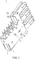
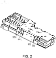
- FIG. 1 and FIG. 2 are structural schematic diagrams of a terminal assembly of the first embodiment of the present disclosure.
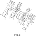
- FIG. 3 is an exploded view of the terminal assembly of the first embodiment of the present disclosure.
- the terminal assembly 1 comprises a first terminal component 2, a second terminal component 3, at least one metal shielding plate 4, and a metal housing 5.
- FIG. 4 and FIG. 5 are structural schematic diagrams of a first terminal component of the first embodiment of the present disclosure. As shown in FIG. 3 to FIG. 5 ,
- the first terminal component 2 of this embodiment further comprises a first insulating body 22.
- the plurality of first signal terminals 21 is embedded in the first insulating body 22.
- Each of the first signal terminals 21 comprises a first plugging end 21a and a first connecting end 21b.
- the first plugging end 21a and the first connecting end 21b respectively protrudes from the first insulating body 22.
- the first plugging end 21a is used for electrically contacting with a mating connector.
- the first connecting end 21b is used for being mounted to the circuit board.
- the first insulating body 22 comprises at least one first through groove 23 laterally penetrating the first insulating body 22, but it is not limited thereto.
- the first insulating body 22 and the plurality of first signal terminals 21 are integrated as an integral member through injection molding, but it is not limited thereto.
- the second terminal component 3 is disposed opposite to the first terminal component 2.
- the second terminal component 3 comprises a plurality of second signal terminals 31.
- the plurality of first signal terminals 21 are disposed in corresponding to the plurality of second signal terminals 31, respectively.
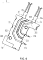
- FIG. 6 and FIG. 7 are structural schematic diagrams of a second terminal component of the first embodiment of the present disclosure.
- the second terminal component 3 of this embodiment further comprises a second insulating body 32.
- the plurality of second signal terminals 31 is embedded in the second insulating body 32.
- the second insulating body 32 corresponds to the first insulating body 22.
- Each of the second signal terminals 31 comprises a second plugging end 31a and a second connecting end 31b.
- the second plugging end 31a and the second connecting end 31b respectively protrudes from the second insulating body 32.
- the second plugging end 31a is used for electrically contacting with a mating connector.
- the second connecting end 31b is for being mounted to the circuit board.
- the second plugging end 31a of each of the second signal terminals 31 corresponds to the first plugging end 21a of each of the first signal terminals 21 and is disposed on the same side.
- the second connecting end 31b of each of the second signal terminals 31 corresponds to the first connecting end 21b of each of the first signal terminals 21 and is disposed on the same side.
- the second insulating body 32 comprises at least one second through groove 33 penetrating the second insulating body 32.
- the second through groove 33 is aligned with the first through groove 23, but it is not limited thereto.
- the second insulating body 32 and the plurality of second signal terminals 31 are integrated as an integral member through injection molding, but it is not limited thereto.
- At least one metal shielding plate 4 connects with the first terminal component 2 and the second terminal component 3.
- the metal shielding plate 4 is disposed between two adjacent first signal terminals 21 and between two adjacent second signal terminals 31, so as to separate a plurality of first signal terminals 21 and a plurality of second signal terminals 31.
- Each metal shielding plate 4 of this embodiment is disposed in the corresponding first through groove 23 and second through groove 33, but it is not limited thereto.
- the metal housing 5 covers the first terminal component 2, the second terminal component 3, and at least one metal shielding plate 4. Two opposite sides of the metal shielding plate 4 are connected to the metal housing 5.
- the metal housing 5 of this embodiment comprises a plurality of ground plugging ends 5a, and a plurality of ground connecting ends 5b.
- the plurality of ground plugging ends 5a correspond to a first plugging end 21a and a second plugging end 31a and are disposed on the same side for itself to be electrically contacted with the mating connector.
- the plurality of ground connecting ends 5b correspond to a first connecting end 21b and a second connecting end 31b and are disposed on the same side for itself to be mounted onto the circuit board.
- the metal shielding plate 4 is connected to the metal housing 5 to be grounded to electromagnetically shield the first terminal component 2 and the second terminal component 3.
- the first terminal component 2 comprises a first insulating body 22 and two first signal terminals 21 embedded in the first insulating body 22.
- the first insulating body 22 and the two first signal terminals 21 are integrated as an integral member through injection molding.
- the first insulating body 22 comprises a first through groove 23 disposed between the two first signal terminals 21.
- the second terminal component 3 comprises a second insulating body 32 and two second signal terminals 31 embedded in the second insulating body 32.
- the second insulating body 32 and the two second signal terminals 31 are integrated as an integral member through injection molding.
- the second insulating body 32 comprises a second through groove 33.
- the second through groove 33 is disposed between the two second signal terminals 31 and is aligned with the first through groove 23.
- the number of metal shielding plates 4 is one.
- the metal shielding plate 4 is fixedly accommodated in the first through groove 23 and the second through groove 33.
- the metal housing 5 covers the first terminal component 2, the second terminal component 3, and the metal shielding plate 4.
- the opposite two sides of the metal shielding plate 4 are connected to the metal housing 5. Since the first terminal component 2 and the second terminal component 3 are injection molded parts, when assembling, it only needs to assemble the first terminal component 2, the metal shielding plate 4, and the second terminal component 3 according to the assembly order, followed by installing them into the metal housing 5. Finally, to solder the metal shielding plate 4 with the metal housing 5.
- the assembling steps can be minimized and the assembling efficiency can be improved to put the automated manufacturing into practice with laser spot soldering as preferred.
- FIG. 8 is a structural schematic diagram of a metal shielding plate of the first embodiment of the present disclosure.
- a plurality of third positioning columns 41 are disposed on two opposite sides of the metal shielding plate 4 respectively.
- the plurality of third positioning columns 41 are exposed from the at least one first through groove 23 and the at least one second through groove 33.
- a plurality of third positioning holes 51 are disposed on the metal housing 5 (see FIG. 1 ).
- Each of the third positioning columns 41 is disposed in the corresponding third positioning hole 51.
- the two opposite sides of the metal shielding plate 4 are respectively provided with two third positioning columns 41, and the number of third positioning holes 51 is four. It can be seen that the four third positioning holes 51 are respectively disposed on two sides of the metal housing 5, and the two third positioning columns 41 on one side of the metal shielding plate 4 are correspondingly inserted into the two third positioning holes 51 on one side of the metal housing 5.
- the present disclosure would not be limited thereto.
- the numbers of the plurality of third positioning columns 41 could be different.
- the numbers of the plurality of third positioning columns 41 could be three, four, five, six or more than six.
- an inner surface of the metal housing 5 comprises a plurality of soldering bumps 52 corresponding to the metal shielding plate 4 in the first through groove 23 and the second through groove 33, for facilitating the laser spot soldering connection between the metal shielding plate 4 and the metal housing 5.
- the inner surface of the metal housing 5 comprises a plurality of soldering bumps 52.
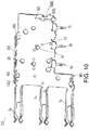
- FIG. 9 and FIG. 10 are structural schematic diagrams of a first housing of the first embodiment of the present disclosure.
- FIG. 11 and FIG. 12 are structural schematic diagrams of a second housing of the first embodiment of the present disclosure.
- the number of the plurality of soldering bumps 52 is twenty.
- the metal housing 5 comprises a first housing 501 and a second housing 502.
- Ten soldering bumps 52 are disposed on an inner surface of the first housing 501 of the metal housing 5, and the other ten soldering bumps 52 are disposed on an inner surface of the second housing 502 of the metal housing 5.
- the ten soldering bumps 52 in the first housing 501 and the ten soldering bumps 52 in the second housing 502 are respectively disposed along a path of the metal shielding plate 4.
- each metal shielding plate 4 is connected to the first housing 501 on one side protruding from the first insulating body 22, and each metal shielding plate 4 is connected to the second housing 502 on one side protruding from the second insulating body 22.
- the metal shielding plate 4 and the first housing 501 and the second housing 502 are laser spot soldered on the twenty soldering bumps 52, and the metal shielding plate 4 is fixedly connected to the metal housing 5.
- the shielding metal Due to the difficulty of adopting rigid mechanical configuration for the shielding metal and the metal housing 5 of the prior art, the shielding metal usually uses conductive plastic insert molded parts, which is mainly connected to the metal housing 5 by hot melting contact of the plastic column.
- the metal shielding plate 4 and the metal housing 5 are laser spot soldered through a plurality of soldering bumps 52 to realize a rigid mechanical connection between the metal shielding plate 4 and the metal housing 5, which increases assembling speed.
- solder bumps 52 it only takes twenty solder bumps 52 in the above description as an example for the description of the plurality of soldering bumps 52, but the present disclosure is not limited thereto.
- the terminal assembly 1 can be used as a wafer of a high speed backplane connector.
- the first insulating body 22 of the first terminal component 2 and the second insulating body 32 of the second terminal component 3 are vertical wafers.
- the first signal terminals 21 of the first terminal component 2 are arranged along a vertical surface of the first insulating body 22, and the second signal terminals 31 of the second terminal component 3 are arranged along a vertical surface of the second insulating body 32.
- the above example is only an embodiment of the present disclosure.
- the terminal assembly 1 of this embodiment could also be applied to other types of connectors, which would not be repeated again herein.
- the first housing 501 is disposed on the first terminal component 2 and comprises a plurality of first flanges 503 on its periphery. Each of the first flanges 503 is provided with a buckle opening 5031.
- the second housing 502 is disposed on the second terminal component 3 and comprises a plurality of second flanges 504 on its periphery. Each of the second flanges 504 is also provided with a buckle 5041 corresponding to the buckle opening 5031 on each of the first flanges 503.
- Each of the second flanges 504 covers the corresponding first flange 503.
- at least one of the first flanges 503 of this embodiment is further provided with a plurality of elastic pieces 5033.
- the plurality of elastic pieces 5033 are in contact with an inner surface of the corresponding second flange 504, so as to increase the stability of the electrical connection between the first flange 503 and the second flange 504, and to prevent the connection from shaking caused by the existence of gaps, but it is not limited thereto.
- FIG. 13 is an enlarged view of area A of FIG. 11 .
- one end of the buckle 5041 close to the inside of the second housing 502 of this embodiment comprises an abutting surface 5042 abutting against a sidewall of the buckle opening 5031 close to the second housing 502, but it is not limited thereto.
- the buckle opening 5031 of this embodiment comprises an insertion part 54 and a positioning part 55.
- the buckle 5041 enters the positioning part 55 through the insertion part 54, and the abutting surface 5042 abuts against a sidewall of the positioning part 55.
- the width of the positioning part 55 is greater than the width of the insertion part 54.
- a side edge of the insertion part 54 abuts against the buckle 5041 and two opposite surfaces perpendicular to the abutting surface 5042. So, the interlocking connection between the first housing 501 and the second housing 502 can be realized, but it is not limited thereto.
- the buckle 5041 is a bump protruding inward from a surface of the second flange 504.
- the abutting surface 5042 is an outer surface of the bump
- the insertion part 54 is a vertical through groove
- the positioning part 55 is a horizontal through groove.
- the insertion part 54 and the positioning part 55 form a T-shaped groove complex.
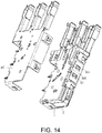
- FIG. 14 is a partially exploded view of the terminal assembly of the first embodiment of the present disclosure.
- an end part of each of the first flanges 503 facing the second housing 502 comprises a guiding member 5032 extending away from the corresponding second flange 504.
- a side surface of the second insulating body 32 is also provided with a plurality of guiding grooves 324, and each of the guiding members 5032 is disposed in a corresponding guiding groove 324.
- each of the guiding members 5032 is disposed at the top middle position of each first flange 503.
- Each of the guiding members 5032 is bent inwardly in a bumping arc shape and is buckled in the guiding groove 324 corresponding to a side surface of the second insulating body 32, but it is not limited thereto.
- a plurality of first waste guiding grooves 221 are also provided on the first insulating body 22.
- Each of the first waste guiding grooves 221 is disposed on a surface of the first insulating body 22 adjacent to the second insulating body 32 and extends to the corresponding first signal terminal 21.
- a plurality of second waste guiding grooves 321 are also provided on the second insulating body 32.
- Each of the second waste guiding grooves 321 is disposed on a surface of the second insulating body 32 adjacent to the first insulating body 22 and extends to the corresponding second signal terminal 31.
- a plurality of corresponding first waste guiding grooves 221 are disposed on the first insulating body 22, and a plurality of corresponding second waste guiding grooves 321 are disposed on the second insulating body 32 to reduce the dielectric constant, which achieving powerful coupling between the first signal terminal 21 and the second signal terminal 31, but it is not limited thereto.
- a plurality of first positioning columns 222 are disposed on a surface of the first insulating body 22 adjacent to the second insulating body 32, and a plurality of first positioning holes 322 are disposed on a surface of the second insulating body 32 adjacent to the first insulating body 22.
- the plurality of first positioning columns 222 respectively correspond to the first positioning holes 322 and are inserted into the corresponding first positioning holes 322 to allow the first insulating body 22 to position and connect with the second insulating body 32.
- the number of first positioning columns 222 is two, and the number of first positioning holes 322 is two.
- the two first positioning columns 222 are diagonally disposed on the first insulating body 22, and the two first positioning holes 322 are disposed diagonally on the second insulating body 32.
- the two first positioning columns 222 are inserted into the corresponding first positioning holes 322 to allow the first insulating body 22 to position and connect with the second insulating body 32.
- the two first positioning columns 222 and the two first positioning holes 322 are only taken as examples above to describe the plurality of first positioning columns 222 and the plurality of first positioning holes 322, but the present disclosure is not limited thereto.
- the number of the first positioning columns 222 matches the number of the first positioning holes 322.
- the number of the first positioning columns 222 and the number of the first positioning holes 322 could be any other numbers. For example, three, four, five, six or more than six, respectively.
- a surface of the first insulating body 22 away from the second insulating body 32 and a surface of the second insulating body 32 away from the first insulating body 22 are respectively provided with a plurality of second positioning columns 223.
- a plurality of second positioning holes 53 are also disposed on the first housing 501 and the second housing 502. Each second positioning column 223 is inserted into the corresponding second positioning hole 53.
- the number of second positioning columns 223 of this embodiment is four. It can be seen that the two second positioning columns 223 are disposed on a surface of the first insulating body 22 away from the second insulating body 32. The two second positioning columns 223 are disposed on a surface of the second insulating body 32 away from the first insulating body 22.
- each second positioning column 223 could be a hot melt column.
- the above four second positioning columns 223 are taken as examples for the description of the plurality of the second positioning columns 223, but the present disclosure is not limited thereto.
- the number of the plurality of second positioning columns 223 could be any other numbers. For example, three, four, five, six or more than six.
- a first engaging bump 224 and an elastic arm 225 are disposed on a side surface of the first insulating body 22.
- One end of the elastic arm 225 is disposed on the first engaging bump 224, and the other end thereof extends away from the first engaging bump 224.
- the second insulating body 32 is also provided with a second engaging bump 325 adjacent to the first engaging bump 224.
- first engaging bump 224, the second engaging bump 325, and the elastic arm 225 are used for the assembling of the terminal assembly 1 onto a connector insulative housing, they would match with the corresponding structural components of the connector insulative housing to restrict the degree of freedom in the X, Y, and Z axes direction of the terminal assembly 1, wherein the X, Y, Z axes are virtual imaginary degrees of freedom.
- Z axis is the degree of freedom in the vertical direction of terminal assembly 1
- X and Y axis form the freedom degree in the horizontal direction to which the Z axis is perpendicular to.
- a plurality of first retaining grooves 226 are disposed on a surface of the first insulating body 22 away from the second insulating body 32.
- Each of the first signal terminals 21 is disposed between two adjacent first retaining grooves 226, and the plurality of first retaining grooves 226 respectively form a first retaining space with the first housing 501.
- a plurality of second retaining grooves 323 are disposed on a surface of the second insulating body 32 away from the first insulating body 22.
- Each of the second signal terminals 31 is disposed between two adjacent second retaining grooves 323, and the plurality of second retaining grooves 323 respectively form a second retaining space with the second housing 502.
- the structural components of the connector body would interfere with the metal housing 5.
- the first retaining space and the second retaining space provide a space for the metal housing 5 to shrink, the metal housing 5 could still have a certain degree of elasticity, but it is not limited thereto.
- At least one first connecting bridge 231 is disposed on one side of each first through groove 23 close to the metal housing 5, and at least one second connecting bridge 331 is disposed on one side of each second through groove 33 close to the metal housing 5.
- Two opposite sides of each metal shielding plate 4 are correspondingly tenoned onto at least one first connecting bridge 231 and at least one second connecting bridge 331 and are connected to the metal housing 5, but it is not limited thereto.
- two sides of the metal shielding plate 4 of this embodiment comprise a notch 42 corresponding to at least one first connecting bridge 231 and at least one second connecting bridge 331.
- Two sides of the metal shielding plate 4 are tenoned on at least one first connecting bridge 231 and at least one second connecting bridge 331 through the notch 42, but it is not limited thereto.
- two sides of the metal shielding plate 4 are tenoned on at least one first connecting bridge 231 and at least one second connecting bridge 331 through the notch 42.
- the number of notches 42 is six
- the number of at least one of the first connecting bridges 231 is three
- the number of at least one of the second connecting bridges 331 is three. It can be seen that the six notches 42 are symmetrically disposed on two sides of the metal shielding plate 4. Two sides of the metal shielding plate 4 are tenoned on the three first connecting bridges 231 and the three second connecting bridges 331 through the six notches 42.
- first connecting bridges 231 and three second connecting bridges 331 are taken as examples for the description of the plurality of first connecting bridges 231 and the plurality of second connecting bridges 331, but the present disclosure is not limited thereto.
- a plurality of bumps 43 are disposed on two sides of each metal shielding plate 4.
- the metal shielding plate 4 When the metal shielding plate 4 is disposed in a corresponding first through groove 23 and a second through groove 33, the plurality of bumps 43 can be in close contact with an inner wall of the first through groove 23 and the second through groove 33, which is usually interference contact.
- the metal shielding plate 4 can be positioned in the first through groove 23 and in the second through groove 33 to prevent it from shaking in the first through groove 23 and the second through groove 33, which stabilizes the assemble of the related components, but this is not limited thereto.
- FIG. 15 is a structural schematic diagram of a terminal assembly of the second embodiment of the present disclosure.
- FIG. 16 is an exploded view of the terminal assembly of the second embodiment of the present disclosure.
- the terminal assembly 1 of this embodiment is different from that of the first embodiment in that the first terminal component 2 comprises a first insulating body 22 and three first signal terminals 21 embedded in the first insulating body 22.
- the first insulating body 22 and the three first signal terminals 21 are integrated as an integral member through injection molding.
- the first insulating body 22 comprises two first through grooves 23 respectively disposed between two adjacent first signal terminals 21 of the three first signal terminals 21 at an interval.
- the second terminal component 3 comprises a second insulating body 32 and three second signal terminals 31.
- the three second signal terminals 31 are embedded in the second insulating body 32.
- the second insulating body 32 and the three second signal terminals 31 are integrated as an integral member through injection molding.
- the second insulating body 32 comprises two second through grooves 33 respectively disposed between two adjacent second signal terminals 31 of the three second signal terminals 31 at an interval.
- the two second through grooves 33 corresponds to the two first through grooves 23, respectively.
- the number of metal shielding plates 4 is two.
- the two metal shielding plates 4 are respectively disposed in the corresponding first through groove 23 and second through groove 33.
- the metal housing 5 covers the first terminal component 2, the second terminal component 3, and the two metal shielding plates 4. The two opposite sides of the two metal shielding plates 4 are connected to the metal housing 5.
- first terminal component 2 and the second terminal component 3 are injection molded components, when assembling the terminal assembly, it is only necessary to install the first terminal component 2, the two metal shielding plate 4, and the second terminal component 3 in the metal housing 5 in order, followed by secure-connecting the two metal shielding plate 4 with the metal housing 5 by soldering. This would simplify the assembling process, enhance the assembling efficiency, and achieve automated manufacturing.
- first signal terminals 21 and two second signal terminals 31, and only three first signal terminals 21 and three second signal terminals 31 are respectively taken as examples for the description of the plurality of first signal terminals 21 and the plurality of second signal terminals 31, but the present disclosure is not limited thereto.
- the number of the plurality of first signal terminals 21 and the number of the plurality of second signal terminals 31 could be any other numbers.
- the number of the plurality of first signal terminals 21 could be four, five, six or more than six
- the number of the plurality of second signal terminals 31 could be four, five, six or more than six.
- FIG. 17 is a structural schematic diagram of a connector of the third embodiment of the present disclosure.
- a connector 6 comprises an insulative housing 61 and at least two terminal assemblies 1 according to any form of the first embodiment mentioned above, and the terminal assemblies 1 are arranged on inner left and right sides of the insulative housing 61.
- the connector 6 further comprises a partition plate 62.
- the terminal assembly 1 is disposed between the insulative housing 61 and the partition plate 62.
- FIG. 18 is a structural schematic diagram of an insulative housing of the third embodiment of the present disclosure. As shown in FIG. 17 and FIG. 18 , the number of the terminal assemblies 1 is four, and the insulative housing 61 comprises a plurality of insertion holes 611.
- the insulative housing 61 is provided with a limiting gap 622 corresponding to the first engaging bump 224 and the second engaging bump 325 of each of the terminal assemblies 1, and is provided with a limiting opening 613 corresponding to the elastic arm 225 of each of the terminal assemblies 1.
- the four terminal assemblies 1 are installed on the insulative housing 61, and the signal terminals of the four terminal assemblies 1 are correspondingly inserted in the insertion holes 611.
- the first engaging bump 224 and the second engaging bump 325 are disposed in the limiting gap 622.
- the elastic arm 225 abuts against a sidewall of the corresponding limiting opening 613.
- the partition plate 62 covers the four terminal assemblies 1.
- the present disclosure proposed a terminal assembly and connector.
- the present disclosure provides a terminal assembly with a limited amount of parts, which could simplify the assembling process, enhance the assembling efficiency, achieve automated manufacturing, and significantly improve the assembling quality.
- the invention also relates to a terminal assembly and connector, the terminal assembly comprises a first terminal component, a second terminal component, at least one metal shielding plate, and a metal housing.
- the first terminal component comprises a plurality of first signal terminals embedded in the first insulating body.
- the second terminal component comprises a second insulating body and a plurality of second signal terminals embedded in the second insulating body.
- the second terminal component is disposed opposite to the first terminal component.
- the at least one metal shielding plate connects with the first terminal component and the second terminal component.
- the metal shielding plate is disposed between the two adjacent first signal terminals and the two adjacent second signal terminals.
- the metal housing covers the first terminal component, the second terminal component and at least one metal shielding plate.
- the at least one metal shielding plate connects with the metal housing.
Landscapes
- Details Of Connecting Devices For Male And Female Coupling (AREA)
Abstract
Description
- This application claims the priority benefit of
Chinese Patent Application Serial Number CN202010459181.X, filed on May 27, 2020 - The present disclosure relates to the technical field of high speed signal transmission and communication, particularly to a terminal assembly and connector.
- The arrayed installation for conventional high speed connectors require the terminals thereof to be flake shaped. The configuration of a high speed connector in the prior arts usually includes a main metal housing, differential signal terminals, and a metal shell. The differential signal terminals are disposed in the metal housing. The metal shell covers the periphery of the differential signal terminals path to block signal radiation, generating a common mode signal to the ground, which is coupled with other differential signals. This not only having the energy to be consumed from its own but also having the other signals and networks to be interfered and damaged. However, the configuration of high speed connector of the prior art includes an excessive number of parts, resulting in a complicated assembling process, less achievable automated manufacturing, greatly reduced assembling efficiency and unstable assembling quality.
- The embodiments of the present disclosure provide a connector to solve the problem for the configuration of a high speed connector: an excessive number of parts, complicated assembling process, low assembling efficiency, and less achievable automated manufacturing.
- On the first aspect, a terminal assembly is provided, comprising a first terminal component, a second terminal component, at least one metal shielding plate, and a metal housing. The first terminal component comprises a plurality of first signal terminals. The first signal terminal is embedded in the first insulating body. The second terminal component comprises a plurality of second signal terminals and a second insulating body. The second signal terminal is embedded in the second insulating body. The second terminal component is disposed opposite to the first terminal component. The at least one metal shielding plate is connecting with the first terminal component and the second terminal component. The metal shielding plate is disposed between the two adjacent first signal terminals and between the two adjacent second signal terminals. The metal housing covers the first terminal component, the second terminal component and at least one of the metal shielding plates. The at least one of the metal shielding plates is connected to the metal housing.
- In the first possible embodiment of the first aspect, the first insulating body comprises at least one first through groove. The second insulating body comprises at least one second through groove. Each of the metal shielding plates is disposed in the corresponding first through groove and the second through groove. Each of the metal shielding plates is connected to the metal housing.
- Combining with the first possible embodiment of the first aspect, in the second possible embodiment of the first aspect, two opposite sides of the metal shielding plate respectively comprise a plurality of third positioning columns exposed from at least one of the first through grooves and at least one of the second through grooves. The metal housing comprises a plurality of third positioning holes disposed in the corresponding third positioning holes.
- In the third possible embodiment of the first aspect, an inner surface of the metal housing comprises a plurality of soldering bumps soldered to be fixed onto an inner surface of the metal shielding plate.
- In the fourth possible embodiment of the first aspect, the metal housing comprises a first housing and a second housing. The first housing is disposed on the first terminal component. On the periphery of the first housing is provided with a plurality of first flanges, each of which comprises a buckle opening. The second housing is disposed on the second terminal component. On the periphery of the second housing is provided with a plurality of second flanges, each of which comprises a buckle corresponding to the buckle opening of each of the first flanges. Each of the second flanges covers the corresponding first flange. Each of the buckles correspondingly buckles into each of the buckle openings.
- Combining with the fourth possible embodiment of the first aspect, in the fifth possible embodiment of the first aspect, an end part of each of the first flanges facing the second housing comprises a guiding member. Each of the guiding members extends in a direction away from the corresponding second flange. A side surface of the second insulating body is provided with a plurality of guiding grooves. Each of the guiding members is disposed in the corresponding guiding groove.
- Combining with the fourth possible embodiment of the first aspect, in the sixth possible embodiment of the first aspect, one end of the buckle close to the inner side of the second housing comprises an abutting surface abutting against a sidewall of the buckle opening close to the second housing.
- Combining with the sixth possible embodiment of the first aspect, in the seventh possible embodiment of the first aspect, the buckle opening comprises an insertion part and a positioning part. The buckle enters the positioning part through the insertion part. The abutting surface abuts against a sidewall of the positioning part. The width of the positioning part is greater than the width of the insertion part. A side edge of the insertion part abuts against two opposite surfaces of the buckle perpendicular to the abutting surface.
- Combining with the fourth possible embodiment of the first aspect, in the eighth possible embodiment of the first aspect, a plurality of elastic pieces is disposed on at least one of the plurality of first flanges. The plurality of elastic pieces is in contact with an inner surface of the corresponding second flange.
- In the ninth possible embodiment of the first aspect, a plurality of second positioning columns are respectively disposed on a surface of the first insulating body away from the second insulating body and on one side of the second insulating body away from the first insulating body. A plurality of second positioning holes are disposed on the first housing and the second housing. Each of the second positioning columns is inserted into the corresponding second positioning hole. The second positioning column is a hot melt column.
- Combining with the first possible embodiment of the first aspect, in the tenth possible embodiment of the first aspect, at least one first connecting bridge is disposed on one side of each of the first through grooves close to the metal housing. At least one second connecting bridge is disposed on one side of each of the second through grooves close to the metal housing. Two sides of the metal shielding plate comprise a notch corresponding to the at least one first connecting bridge and the at least one second connecting bridge. The two sides of the metal shielding plate are tenoned onto the at least one first connecting bridge and the at least one second connecting bridge through the notches.
- On the second aspect, a connector is provided, comprising an insulative housing and at least two terminal assemblies according to the first aspect. The terminal assemblies are arranged on inner left and right sides of the insulative housing.
- In the embodiments of the present disclosure, when assembling the terminal assembly, it is only necessary to install the first terminal component, the metal shielding plate, and the second terminal component in the metal housing in order, followed by secure-connecting the metal shielding plate with the metal housing by soldering. The present disclosure provides a terminal assembly with a limited amount of parts, which could simplify the assembling process, enhance the assembling efficiency, achieve automated manufacturing, and significantly improve the assembling quality.
- It should be understood, however, that this summary may not contain all aspects and embodiments of the present disclosure, that this summary is not meant to be limiting or restrictive in any manner, and that the disclosure as disclosed herein will be understood by one of ordinary skill in the art to encompass obvious improvements and modifications thereto.
- The features of the exemplary embodiments believed to be novel and the elements and/or the steps characteristic of the exemplary embodiments are set forth with particularity in the appended claims. The Figures are for illustration purposes only and are not drawn to scale. The exemplary embodiments, both as to organization and method of operation, may best be understood by reference to the detailed description which follows taken in conjunction with the accompanying drawings in which:
-
FIG. 1 is a structural schematic diagram of a terminal assembly of the first embodiment of the present disclosure; -
FIG. 2 is a structural schematic diagram of the terminal assembly of the first embodiment of the present disclosure; -
FIG. 3 is an exploded view of the terminal assembly of the first embodiment of the present disclosure; -
FIG. 4 is a structural schematic diagram of a first terminal component of the first embodiment of the present disclosure; -
FIG. 5 is a structural schematic diagram of the first terminal component of the first embodiment of the present disclosure; -
FIG. 6 is a structural schematic diagram of a second terminal component of the first embodiment of the present disclosure; -
FIG. 7 is a structural schematic diagram of the second terminal component of the first embodiment of the present disclosure; -
FIG. 8 is a structural schematic diagram of a metal shielding plate of the first embodiment of the present disclosure; -
FIG. 9 is a structural schematic diagram of a first housing of the first embodiment of the present disclosure; -
FIG. 10 is a structural schematic diagram of the first housing of the first embodiment of the present disclosure; -
FIG. 11 is a structural schematic diagram of a second housing of the first embodiment of the present disclosure; -
FIG. 12 is a structural schematic diagram of the second housing of the first embodiment of the present disclosure; -
FIG. 13 is an enlarged view of area A ofFIG. 11 ; -
FIG. 14 is a partially exploded view of the terminal assembly of the first embodiment of the present disclosure; -
FIG. 15 is a structural schematic diagram of a terminal assembly of the second embodiment of the present disclosure; -
FIG. 16 is an exploded view of the terminal assembly of the second embodiment of the present disclosure; -
FIG. 17 is a structural schematic diagram of a connector of the third embodiment of the present disclosure; and -
FIG. 18 is a structural schematic diagram of an insulative housing of the third embodiment of the present disclosure. - The present disclosure will now be described more fully hereinafter with reference to the accompanying drawings, in which exemplary embodiments of the disclosure are shown. This present disclosure may, however, be embodied in many different forms and should not be construed as limited to the embodiments set forth herein. Rather, these embodiments are provided so that this present disclosure will be thorough and complete, and will fully convey the scope of the present disclosure to those skilled in the art.
- Certain terms are used throughout the description and following claims to refer to particular components. As one skilled in the art will appreciate, manufacturers may refer to a component by different names. This document does not intend to distinguish between components that differ in name but function. In the following description and in the claims, the terms "include/including" and "comprise/comprising" are used in an open-ended fashion, and thus should be interpreted as "including but not limited to". "Substantial/substantially" means, within an acceptable error range, the person skilled in the art may solve the technical problem in a certain error range to achieve the basic technical effect.
- The following description is of the best-contemplated mode of carrying out the disclosure. This description is made for the purpose of illustration of the general principles of the disclosure and should not be taken in a limiting sense. The scope of the disclosure is best determined by reference to the appended claims.
- Moreover, the terms "include", "contain", and any variation thereof are intended to member a non-exclusive inclusion. Therefore, a process, method, object, or device that includes a series of elements not only includes these elements, but also includes other elements not specified expressly, or may include inherent elements of the process, method, object, or device. If no more limitations are made, an element limited by "include a/an ..." does not exclude other same elements existing in the process, the method, the article, or the device which includes the element.
- In the following embodiment, the same reference numerals are used to refer to the same or similar elements throughout the disclosure.
- Regarding the "first", "second", etc. used in this article, it does not specifically refer to the order or sequence, nor is it intended to limit the application, but only to distinguish between components or operations described in the same technical terms.
- In the first embodiment of the present disclosure,
FIG. 1 andFIG. 2 are structural schematic diagrams of a terminal assembly of the first embodiment of the present disclosure.FIG. 3 is an exploded view of the terminal assembly of the first embodiment of the present disclosure. As shown inFIG. 1 andFIG. 2 , theterminal assembly 1 comprises a firstterminal component 2, a secondterminal component 3, at least onemetal shielding plate 4, and ametal housing 5. - Wherein the first
terminal component 2 comprises a plurality offirst signal terminals 21.FIG. 4 andFIG. 5 are structural schematic diagrams of a first terminal component of the first embodiment of the present disclosure. As shown inFIG. 3 to FIG. 5 , - The first
terminal component 2 of this embodiment further comprises a first insulatingbody 22. The plurality offirst signal terminals 21 is embedded in the first insulatingbody 22. Each of thefirst signal terminals 21 comprises a first pluggingend 21a and a first connectingend 21b. The first pluggingend 21a and the first connectingend 21b respectively protrudes from the first insulatingbody 22. The first pluggingend 21a is used for electrically contacting with a mating connector. The first connectingend 21b is used for being mounted to the circuit board. The first insulatingbody 22 comprises at least one first throughgroove 23 laterally penetrating the first insulatingbody 22, but it is not limited thereto. In one embodiment, the first insulatingbody 22 and the plurality offirst signal terminals 21 are integrated as an integral member through injection molding, but it is not limited thereto. - The
second terminal component 3 is disposed opposite to the firstterminal component 2. Thesecond terminal component 3 comprises a plurality ofsecond signal terminals 31. The plurality offirst signal terminals 21 are disposed in corresponding to the plurality ofsecond signal terminals 31, respectively.FIG. 6 andFIG. 7 are structural schematic diagrams of a second terminal component of the first embodiment of the present disclosure. As shown inFIG. 3 ,FIG. 6 , andFIG. 7 , thesecond terminal component 3 of this embodiment further comprises a second insulatingbody 32. The plurality ofsecond signal terminals 31 is embedded in the second insulatingbody 32. The secondinsulating body 32 corresponds to the first insulatingbody 22. Each of thesecond signal terminals 31 comprises a second pluggingend 31a and a secondconnecting end 31b. The second pluggingend 31a and the second connectingend 31b respectively protrudes from the second insulatingbody 32. The second pluggingend 31a is used for electrically contacting with a mating connector. The secondconnecting end 31b is for being mounted to the circuit board. The second pluggingend 31a of each of thesecond signal terminals 31 corresponds to the first pluggingend 21a of each of thefirst signal terminals 21 and is disposed on the same side. The secondconnecting end 31b of each of thesecond signal terminals 31 corresponds to the first connectingend 21b of each of thefirst signal terminals 21 and is disposed on the same side. The secondinsulating body 32 comprises at least one second throughgroove 33 penetrating the second insulatingbody 32. The second throughgroove 33 is aligned with the first throughgroove 23, but it is not limited thereto. In one embodiment, the second insulatingbody 32 and the plurality ofsecond signal terminals 31 are integrated as an integral member through injection molding, but it is not limited thereto. - At least one
metal shielding plate 4 connects with the firstterminal component 2 and thesecond terminal component 3. Themetal shielding plate 4 is disposed between two adjacentfirst signal terminals 21 and between two adjacentsecond signal terminals 31, so as to separate a plurality offirst signal terminals 21 and a plurality ofsecond signal terminals 31. Eachmetal shielding plate 4 of this embodiment is disposed in the corresponding first throughgroove 23 and second throughgroove 33, but it is not limited thereto. - The
metal housing 5 covers the firstterminal component 2, thesecond terminal component 3, and at least onemetal shielding plate 4. Two opposite sides of themetal shielding plate 4 are connected to themetal housing 5. Back toFIG. 3 , themetal housing 5 of this embodiment comprises a plurality of ground plugging ends 5a, and a plurality of ground connecting ends 5b. The plurality of ground plugging ends 5a correspond to a first pluggingend 21a and a second pluggingend 31a and are disposed on the same side for itself to be electrically contacted with the mating connector. The plurality of ground connecting ends 5b correspond to a first connectingend 21b and a secondconnecting end 31b and are disposed on the same side for itself to be mounted onto the circuit board. Themetal shielding plate 4 is connected to themetal housing 5 to be grounded to electromagnetically shield the firstterminal component 2 and thesecond terminal component 3. - Practically, as shown in
FIG. 3 to FIG. 7 , the firstterminal component 2 comprises a first insulatingbody 22 and twofirst signal terminals 21 embedded in the first insulatingbody 22. The first insulatingbody 22 and the twofirst signal terminals 21 are integrated as an integral member through injection molding. The first insulatingbody 22 comprises a first throughgroove 23 disposed between the twofirst signal terminals 21. - The
second terminal component 3 comprises a second insulatingbody 32 and twosecond signal terminals 31 embedded in the second insulatingbody 32. The secondinsulating body 32 and the twosecond signal terminals 31 are integrated as an integral member through injection molding. The secondinsulating body 32 comprises a second throughgroove 33. The second throughgroove 33 is disposed between the twosecond signal terminals 31 and is aligned with the first throughgroove 23. - The number of
metal shielding plates 4 is one. Themetal shielding plate 4 is fixedly accommodated in the first throughgroove 23 and the second throughgroove 33. Themetal housing 5 covers the firstterminal component 2, thesecond terminal component 3, and themetal shielding plate 4. The opposite two sides of themetal shielding plate 4 are connected to themetal housing 5. Since the firstterminal component 2 and thesecond terminal component 3 are injection molded parts, when assembling, it only needs to assemble the firstterminal component 2, themetal shielding plate 4, and thesecond terminal component 3 according to the assembly order, followed by installing them into themetal housing 5. Finally, to solder themetal shielding plate 4 with themetal housing 5. By performing the steps above, the assembling steps can be minimized and the assembling efficiency can be improved to put the automated manufacturing into practice with laser spot soldering as preferred. - In one embodiment,
FIG. 8 is a structural schematic diagram of a metal shielding plate of the first embodiment of the present disclosure. As shown in the figure, a plurality ofthird positioning columns 41 are disposed on two opposite sides of themetal shielding plate 4 respectively. The plurality ofthird positioning columns 41 are exposed from the at least one first throughgroove 23 and the at least one second throughgroove 33. A plurality of third positioning holes 51 are disposed on the metal housing 5 (seeFIG. 1 ). Each of thethird positioning columns 41 is disposed in the correspondingthird positioning hole 51. When the plurality ofthird positioning columns 41 are used to install themetal shielding plate 4, they can be inserted into the corresponding third positioning holes 51 to position themetal shielding plate 4, but it is not limited thereto. - Practically, the two opposite sides of the
metal shielding plate 4 are respectively provided with twothird positioning columns 41, and the number of third positioning holes 51 is four. It can be seen that the four third positioning holes 51 are respectively disposed on two sides of themetal housing 5, and the twothird positioning columns 41 on one side of themetal shielding plate 4 are correspondingly inserted into the two third positioning holes 51 on one side of themetal housing 5. - It should be understood that it only takes two
third positioning columns 41 in the above description as an example for the description of the plurality ofthird positioning columns 41, but the present disclosure would not be limited thereto. The numbers of the plurality ofthird positioning columns 41 could be different. For example, the numbers of the plurality ofthird positioning columns 41 could be three, four, five, six or more than six. - In one embodiment, an inner surface of the
metal housing 5 comprises a plurality of soldering bumps 52 corresponding to themetal shielding plate 4 in the first throughgroove 23 and the second throughgroove 33, for facilitating the laser spot soldering connection between themetal shielding plate 4 and themetal housing 5. - Practically, the inner surface of the
metal housing 5 comprises a plurality of soldering bumps 52.FIG. 9 andFIG. 10 are structural schematic diagrams of a first housing of the first embodiment of the present disclosure.FIG. 11 andFIG. 12 are structural schematic diagrams of a second housing of the first embodiment of the present disclosure. As shown inFIG. 9 to FIG. 12 , the number of the plurality of soldering bumps 52 is twenty. It can be seen that themetal housing 5 comprises afirst housing 501 and asecond housing 502. Ten soldering bumps 52 are disposed on an inner surface of thefirst housing 501 of themetal housing 5, and the other tensoldering bumps 52 are disposed on an inner surface of thesecond housing 502 of themetal housing 5. The tensoldering bumps 52 in thefirst housing 501 and the tensoldering bumps 52 in thesecond housing 502 are respectively disposed along a path of themetal shielding plate 4. - When the assembling of the
terminal assembly 1 is completed, i.e., when themetal housing 5 covers the firstterminal component 2, thesecond terminal component 3, and themetal shielding plate 4, eachmetal shielding plate 4 is connected to thefirst housing 501 on one side protruding from the first insulatingbody 22, and eachmetal shielding plate 4 is connected to thesecond housing 502 on one side protruding from the second insulatingbody 22. In this way, themetal shielding plate 4 and thefirst housing 501 and thesecond housing 502 are laser spot soldered on the twentysoldering bumps 52, and themetal shielding plate 4 is fixedly connected to themetal housing 5. - Due to the difficulty of adopting rigid mechanical configuration for the shielding metal and the
metal housing 5 of the prior art, the shielding metal usually uses conductive plastic insert molded parts, which is mainly connected to themetal housing 5 by hot melting contact of the plastic column. In theterminal assembly 1 of this embodiment, themetal shielding plate 4 and themetal housing 5 are laser spot soldered through a plurality of soldering bumps 52 to realize a rigid mechanical connection between themetal shielding plate 4 and themetal housing 5, which increases assembling speed. - It should be understood that it only takes twenty
solder bumps 52 in the above description as an example for the description of the plurality of soldering bumps 52, but the present disclosure is not limited thereto. - In one embodiment, the
terminal assembly 1 can be used as a wafer of a high speed backplane connector. The first insulatingbody 22 of the firstterminal component 2 and the second insulatingbody 32 of thesecond terminal component 3 are vertical wafers. Thefirst signal terminals 21 of the firstterminal component 2 are arranged along a vertical surface of the first insulatingbody 22, and thesecond signal terminals 31 of thesecond terminal component 3 are arranged along a vertical surface of the second insulatingbody 32. The above example is only an embodiment of the present disclosure. Theterminal assembly 1 of this embodiment could also be applied to other types of connectors, which would not be repeated again herein. - In one embodiment, back to
FIG. 9 to FIG. 12 , thefirst housing 501 is disposed on the firstterminal component 2 and comprises a plurality offirst flanges 503 on its periphery. Each of thefirst flanges 503 is provided with abuckle opening 5031. Thesecond housing 502 is disposed on thesecond terminal component 3 and comprises a plurality ofsecond flanges 504 on its periphery. Each of thesecond flanges 504 is also provided with abuckle 5041 corresponding to thebuckle opening 5031 on each of thefirst flanges 503. - Each of the
second flanges 504 covers the correspondingfirst flange 503. Back toFIG. 10 , at least one of thefirst flanges 503 of this embodiment is further provided with a plurality ofelastic pieces 5033. The plurality ofelastic pieces 5033 are in contact with an inner surface of the correspondingsecond flange 504, so as to increase the stability of the electrical connection between thefirst flange 503 and thesecond flange 504, and to prevent the connection from shaking caused by the existence of gaps, but it is not limited thereto. - Each
buckle 5041 is correspondingly embedded into eachbuckle opening 5031.FIG. 13 is an enlarged view of area A ofFIG. 11 . As shown inFIG. 11 andFIG. 13 , one end of thebuckle 5041 close to the inside of thesecond housing 502 of this embodiment comprises anabutting surface 5042 abutting against a sidewall of thebuckle opening 5031 close to thesecond housing 502, but it is not limited thereto. Back toFIG. 10 , thebuckle opening 5031 of this embodiment comprises aninsertion part 54 and apositioning part 55. Thebuckle 5041 enters thepositioning part 55 through theinsertion part 54, and theabutting surface 5042 abuts against a sidewall of thepositioning part 55. The width of thepositioning part 55 is greater than the width of theinsertion part 54. A side edge of theinsertion part 54 abuts against thebuckle 5041 and two opposite surfaces perpendicular to theabutting surface 5042. So, the interlocking connection between thefirst housing 501 and thesecond housing 502 can be realized, but it is not limited thereto. - Practically, as shown in
FIG.9 to FIG. 13 , it can be seen that thebuckle 5041 is a bump protruding inward from a surface of thesecond flange 504. The abuttingsurface 5042 is an outer surface of the bump, theinsertion part 54 is a vertical through groove, and thepositioning part 55 is a horizontal through groove. Theinsertion part 54 and thepositioning part 55 form a T-shaped groove complex. - In one embodiment,
FIG. 14 is a partially exploded view of the terminal assembly of the first embodiment of the present disclosure. As shown inFIG. 7 ,FIG. 9 , andFIG. 14 , an end part of each of thefirst flanges 503 facing thesecond housing 502 comprises a guidingmember 5032 extending away from the correspondingsecond flange 504. A side surface of the second insulatingbody 32 is also provided with a plurality of guidinggrooves 324, and each of the guidingmembers 5032 is disposed in acorresponding guiding groove 324. - Practically, each of the guiding
members 5032 is disposed at the top middle position of eachfirst flange 503. Each of the guidingmembers 5032 is bent inwardly in a bumping arc shape and is buckled in the guidinggroove 324 corresponding to a side surface of the second insulatingbody 32, but it is not limited thereto. - In one embodiment, back to
FIG. 5 andFIG. 6 , a plurality of firstwaste guiding grooves 221 are also provided on the first insulatingbody 22. Each of the firstwaste guiding grooves 221 is disposed on a surface of the first insulatingbody 22 adjacent to the second insulatingbody 32 and extends to the correspondingfirst signal terminal 21. A plurality of secondwaste guiding grooves 321 are also provided on the second insulatingbody 32. Each of the secondwaste guiding grooves 321 is disposed on a surface of the second insulatingbody 32 adjacent to the first insulatingbody 22 and extends to the correspondingsecond signal terminal 31. - In this embodiment, a plurality of corresponding first
waste guiding grooves 221 are disposed on the first insulatingbody 22, and a plurality of corresponding secondwaste guiding grooves 321 are disposed on the second insulatingbody 32 to reduce the dielectric constant, which achieving powerful coupling between thefirst signal terminal 21 and thesecond signal terminal 31, but it is not limited thereto. - In one embodiment, back to
FIG. 5 andFIG. 6 , a plurality offirst positioning columns 222 are disposed on a surface of the first insulatingbody 22 adjacent to the second insulatingbody 32, and a plurality of first positioning holes 322 are disposed on a surface of the second insulatingbody 32 adjacent to the first insulatingbody 22. The plurality offirst positioning columns 222 respectively correspond to the first positioning holes 322 and are inserted into the corresponding first positioning holes 322 to allow the first insulatingbody 22 to position and connect with the second insulatingbody 32. - Practically, in this embodiment, the number of
first positioning columns 222 is two, and the number of first positioning holes 322 is two. The twofirst positioning columns 222 are diagonally disposed on the first insulatingbody 22, and the two first positioning holes 322 are disposed diagonally on the second insulatingbody 32. The twofirst positioning columns 222 are inserted into the corresponding first positioning holes 322 to allow the first insulatingbody 22 to position and connect with the second insulatingbody 32. - It should be understood that the two
first positioning columns 222 and the two first positioning holes 322 are only taken as examples above to describe the plurality offirst positioning columns 222 and the plurality of first positioning holes 322, but the present disclosure is not limited thereto. The number of thefirst positioning columns 222 matches the number of the first positioning holes 322. The number of thefirst positioning columns 222 and the number of the first positioning holes 322 could be any other numbers. For example, three, four, five, six or more than six, respectively. - In one embodiment, back to
FIG. 4 andFIG. 7 , a surface of the first insulatingbody 22 away from the second insulatingbody 32 and a surface of the second insulatingbody 32 away from the first insulatingbody 22 are respectively provided with a plurality ofsecond positioning columns 223. A plurality of second positioning holes 53 are also disposed on thefirst housing 501 and thesecond housing 502. Eachsecond positioning column 223 is inserted into the correspondingsecond positioning hole 53. - Practically, the number of
second positioning columns 223 of this embodiment is four. It can be seen that the twosecond positioning columns 223 are disposed on a surface of the first insulatingbody 22 away from the second insulatingbody 32. The twosecond positioning columns 223 are disposed on a surface of the second insulatingbody 32 away from the first insulatingbody 22. - When the first insulating
body 22 and the second insulatingbody 32 are installed in themetal housing 5, the first insulatingbody 22 and the second insulatingbody 32 are respectively installed on thefirst housing 501 and thesecond housing 502, and the foursecond positioning columns 223 are inserted into the corresponding second positioning holes 53. In this way, thefirst housing 501 can be preliminarily positioned on the first insulatingbody 22 and thesecond housing 502 can be preliminarily positioned on the second insulatingbody 32. In one embodiment, eachsecond positioning column 223 could be a hot melt column. Before themetal shielding plate 4 to be laser soldered to themetal housing 5, thefirst housing 501 can be fixed on the first insulatingbody 22, and thesecond housing 502 can be fixed on the second insulatingbody 32 by performing hot melt processing to eachsecond positioning column 223. - It should be understood that the above four
second positioning columns 223 are taken as examples for the description of the plurality of thesecond positioning columns 223, but the present disclosure is not limited thereto. The number of the plurality ofsecond positioning columns 223 could be any other numbers. For example, three, four, five, six or more than six. - In one embodiment, back to
FIG. 5 andFIG. 7 , a firstengaging bump 224 and anelastic arm 225 are disposed on a side surface of the first insulatingbody 22. One end of theelastic arm 225 is disposed on the firstengaging bump 224, and the other end thereof extends away from the firstengaging bump 224. The secondinsulating body 32 is also provided with a secondengaging bump 325 adjacent to the firstengaging bump 224. When the firstengaging bump 224, the secondengaging bump 325, and theelastic arm 225 are used for the assembling of theterminal assembly 1 onto a connector insulative housing, they would match with the corresponding structural components of the connector insulative housing to restrict the degree of freedom in the X, Y, and Z axes direction of theterminal assembly 1, wherein the X, Y, Z axes are virtual imaginary degrees of freedom. Z axis is the degree of freedom in the vertical direction ofterminal assembly 1, and X and Y axis form the freedom degree in the horizontal direction to which the Z axis is perpendicular to. - In one embodiment, back to
FIG. 4 andFIG. 7 , a plurality of first retaininggrooves 226 are disposed on a surface of the first insulatingbody 22 away from the second insulatingbody 32. Each of thefirst signal terminals 21 is disposed between two adjacent first retaininggrooves 226, and the plurality of first retaininggrooves 226 respectively form a first retaining space with thefirst housing 501. A plurality of second retaininggrooves 323 are disposed on a surface of the second insulatingbody 32 away from the first insulatingbody 22. Each of thesecond signal terminals 31 is disposed between two adjacent second retaininggrooves 323, and the plurality of second retaininggrooves 323 respectively form a second retaining space with thesecond housing 502. When theterminal assembly 1 is installed to the connector body, the structural components of the connector body would interfere with themetal housing 5. As the first retaining space and the second retaining space provide a space for themetal housing 5 to shrink, themetal housing 5 could still have a certain degree of elasticity, but it is not limited thereto. - In one embodiment, refer to
FIG. 4 to FIG. 7 again, at least one first connectingbridge 231 is disposed on one side of each first throughgroove 23 close to themetal housing 5, and at least one second connectingbridge 331 is disposed on one side of each second throughgroove 33 close to themetal housing 5. Two opposite sides of eachmetal shielding plate 4 are correspondingly tenoned onto at least one first connectingbridge 231 and at least one second connectingbridge 331 and are connected to themetal housing 5, but it is not limited thereto. Referring toFIG. 8 again, two sides of themetal shielding plate 4 of this embodiment comprise anotch 42 corresponding to at least one first connectingbridge 231 and at least one second connectingbridge 331. Two sides of themetal shielding plate 4 are tenoned on at least one first connectingbridge 231 and at least one second connectingbridge 331 through thenotch 42, but it is not limited thereto. - Practically, two sides of the
metal shielding plate 4 are tenoned on at least one first connectingbridge 231 and at least one second connectingbridge 331 through thenotch 42. As shown inFIG. 4 to FIG. 8 , the number ofnotches 42 is six, the number of at least one of the first connectingbridges 231 is three, and the number of at least one of the second connectingbridges 331 is three. It can be seen that the sixnotches 42 are symmetrically disposed on two sides of themetal shielding plate 4. Two sides of themetal shielding plate 4 are tenoned on the three first connectingbridges 231 and the three second connectingbridges 331 through the sixnotches 42. - It should be understood that, in the foregoing, only three first connecting
bridges 231 and three second connectingbridges 331 are taken as examples for the description of the plurality of first connectingbridges 231 and the plurality of second connectingbridges 331, but the present disclosure is not limited thereto. - Back to
FIG. 8 , in one embodiment, a plurality ofbumps 43 are disposed on two sides of eachmetal shielding plate 4. When themetal shielding plate 4 is disposed in a corresponding first throughgroove 23 and a second throughgroove 33, the plurality ofbumps 43 can be in close contact with an inner wall of the first throughgroove 23 and the second throughgroove 33, which is usually interference contact. Thus, themetal shielding plate 4 can be positioned in the first throughgroove 23 and in the second throughgroove 33 to prevent it from shaking in the first throughgroove 23 and the second throughgroove 33, which stabilizes the assemble of the related components, but this is not limited thereto. - In the second embodiment of the present disclosure,
FIG. 15 is a structural schematic diagram of a terminal assembly of the second embodiment of the present disclosure.FIG. 16 is an exploded view of the terminal assembly of the second embodiment of the present disclosure. As shown in the figures, theterminal assembly 1 of this embodiment is different from that of the first embodiment in that the firstterminal component 2 comprises a first insulatingbody 22 and threefirst signal terminals 21 embedded in the first insulatingbody 22. The first insulatingbody 22 and the threefirst signal terminals 21 are integrated as an integral member through injection molding. The first insulatingbody 22 comprises two first throughgrooves 23 respectively disposed between two adjacentfirst signal terminals 21 of the threefirst signal terminals 21 at an interval. - The
second terminal component 3 comprises a second insulatingbody 32 and threesecond signal terminals 31. The threesecond signal terminals 31 are embedded in the second insulatingbody 32. The secondinsulating body 32 and the threesecond signal terminals 31 are integrated as an integral member through injection molding. The secondinsulating body 32 comprises two second throughgrooves 33 respectively disposed between two adjacentsecond signal terminals 31 of the threesecond signal terminals 31 at an interval. The two second throughgrooves 33 corresponds to the two first throughgrooves 23, respectively. - The number of
metal shielding plates 4 is two. The twometal shielding plates 4 are respectively disposed in the corresponding first throughgroove 23 and second throughgroove 33. Themetal housing 5 covers the firstterminal component 2, thesecond terminal component 3, and the twometal shielding plates 4. The two opposite sides of the twometal shielding plates 4 are connected to themetal housing 5. - Since the first
terminal component 2 and thesecond terminal component 3 are injection molded components, when assembling the terminal assembly, it is only necessary to install the firstterminal component 2, the twometal shielding plate 4, and thesecond terminal component 3 in themetal housing 5 in order, followed by secure-connecting the twometal shielding plate 4 with themetal housing 5 by soldering. This would simplify the assembling process, enhance the assembling efficiency, and achieve automated manufacturing. - It should be understood that, in the foregoing, only two
first signal terminals 21 and twosecond signal terminals 31, and only threefirst signal terminals 21 and threesecond signal terminals 31 are respectively taken as examples for the description of the plurality offirst signal terminals 21 and the plurality ofsecond signal terminals 31, but the present disclosure is not limited thereto. The number of the plurality offirst signal terminals 21 and the number of the plurality ofsecond signal terminals 31 could be any other numbers. For example, the number of the plurality offirst signal terminals 21 could be four, five, six or more than six, and the number of the plurality ofsecond signal terminals 31 could be four, five, six or more than six. - In the third embodiment of the present disclosure,
FIG. 17 is a structural schematic diagram of a connector of the third embodiment of the present disclosure. As shown in the figure, a connector 6 comprises aninsulative housing 61 and at least twoterminal assemblies 1 according to any form of the first embodiment mentioned above, and theterminal assemblies 1 are arranged on inner left and right sides of theinsulative housing 61. - Practically, the connector 6 further comprises a partition plate 62. The
terminal assembly 1 is disposed between theinsulative housing 61 and the partition plate 62.FIG. 18 is a structural schematic diagram of an insulative housing of the third embodiment of the present disclosure. As shown inFIG. 17 andFIG. 18 , the number of theterminal assemblies 1 is four, and theinsulative housing 61 comprises a plurality of insertion holes 611. Theinsulative housing 61 is provided with a limitinggap 622 corresponding to the firstengaging bump 224 and the secondengaging bump 325 of each of theterminal assemblies 1, and is provided with a limiting opening 613 corresponding to theelastic arm 225 of each of theterminal assemblies 1. - It can be seen that the four
terminal assemblies 1 are installed on theinsulative housing 61, and the signal terminals of the fourterminal assemblies 1 are correspondingly inserted in the insertion holes 611. The firstengaging bump 224 and the secondengaging bump 325 are disposed in the limitinggap 622. Theelastic arm 225 abuts against a sidewall of the corresponding limiting opening 613. The partition plate 62 covers the fourterminal assemblies 1. - It should be noted that only the above configuration is taken as an example for the description of one of the plurality of connectors 6, but the present disclosure is not limited thereto. Those skilled in the art can also select other configurations of the connector 6 including the
terminal assembly 1 of the present disclosure according to the teaching of this embodiment. - In summary, the present disclosure proposed a terminal assembly and connector. When assembling the terminal assembly, it is only necessary to install the first terminal component, the metal shielding plate, and the second terminal component in the metal housing in order, followed by secure-connecting the metal shielding plate with the metal housing by soldering. The present disclosure provides a terminal assembly with a limited amount of parts, which could simplify the assembling process, enhance the assembling efficiency, achieve automated manufacturing, and significantly improve the assembling quality.
- It is to be understood that the term "comprises", "comprising", or any other variants thereof, is intended to encompass a non-exclusive inclusion, such that a process, method, article, or device of a series of elements not only include those elements but also comprises other elements that are not explicitly listed, or elements that are inherent to such a process, method, article, or device. An element defined by the phrase "comprising a..." does not exclude the presence of the same element in the process, method, article, or device that comprises the element.
- Although the present disclosure has been explained in relation to its preferred embodiment, it does not intend to limit the present disclosure. It will be apparent to those skilled in the art having regard to this present disclosure that other modifications of the exemplary embodiments beyond those embodiments specifically described here may be made without departing from the spirit of the disclosure. Accordingly, such modifications are considered within the scope of the disclosure as limited solely by the appended claims.
- Accordingly, the invention also relates to a terminal assembly and connector, the terminal assembly comprises a first terminal component, a second terminal component, at least one metal shielding plate, and a metal housing. The first terminal component comprises a plurality of first signal terminals embedded in the first insulating body. The second terminal component comprises a second insulating body and a plurality of second signal terminals embedded in the second insulating body. The second terminal component is disposed opposite to the first terminal component. The at least one metal shielding plate connects with the first terminal component and the second terminal component. The metal shielding plate is disposed between the two adjacent first signal terminals and the two adjacent second signal terminals. The metal housing covers the first terminal component, the second terminal component and at least one metal shielding plate. The at least one metal shielding plate connects with the metal housing.
Claims (12)
- A terminal assembly (1), comprising:a first terminal component (2) comprising a plurality of first signal terminals (21) and a first insulating body (22), the first signal terminals (21) being embedded in the first insulating body (22);a second terminal component (3) comprising a plurality of second signal terminals (31) and a second insulating body (32), the second signal terminals (31) being embedded in the second insulating body (32), the second terminal component (3) being disposed opposite to the first terminal component (2);at least one metal shielding plate (4) connecting with the first terminal component (2) and the second terminal component (3), the metal shielding plate (4) being disposed between the two adjacent first signal terminals (21) and between the two adjacent second signal terminals (31); anda metal housing (5) covering the first terminal component (2), the second terminal component (3) and at least one of the metal shielding plates (4), at least one of the metal shielding plates (4) being connected to the metal housing (5).
- The terminal assembly (1) according to claim 1, characterized in that the first insulating body (22) comprises at least one first through groove (23); the second insulating body (32) comprises at least one second through groove (33);
characterized in that each of the metal shielding plates (4) is disposed in the corresponding first through groove (23) and the second through groove (33); each of the metal shielding plates (4) is connected to the metal housing (5). - The terminal assembly (1) according to claim 2, characterized in that two opposite sides of the metal shielding plate (4) respectively comprise a plurality of third positioning columns (41) exposed from at least one of the first through grooves (23) and at least one of the second through grooves (33); the metal housing (5) comprises a plurality of third positioning holes (51); the third positioning column (41) is disposed in the corresponding third positioning holes (51).
- The terminal assembly (1) according to any of the preceding claims, characterized in that an inner surface of the metal housing (5) comprises a plurality of soldering bumps (52) soldered to be fixed onto an inner surface of the metal shielding plate (4).
- The terminal assembly (1) according to any of the preceding claims, characterized in that the metal housing comprises:a first housing (501) disposed on the first terminal component (2), the first housing (501) being provided with a plurality of first flanges (503) on a periphery thereof; each of the flanges (503) comprises a buckle opening (5031); anda second housing (502) disposed on the second terminal component (3), the second housing (502) being provided with a plurality of second flanges (504) on a periphery thereof; each of the second flanges (504) comprises a buckle (5041) corresponding to the buckle opening (5031) of each of the first flanges (503); each of the second flanges (504) covers the corresponding first flange (503); each of the buckles (5041) correspondingly buckles into each of the buckle openings (5031).
- The terminal assembly (1) according to claim 5, characterized in that an end part of each of the first flanges (503) facing the second housing (502) comprises a guiding member (5032); each of the guiding members (5032) extends in a direction away from the corresponding second flange (504); a side surface of the second insulating body (32) is provided with a plurality of guiding grooves (324); each of the guiding members (5032) is disposed in the corresponding guiding groove (324).
- The terminal assembly (1) according to claim 5 or 6, characterized in that one end of the buckle (5041) close to the inner side of the second housing (502) comprises an abutting surface (5042) abutting against a sidewall of the buckle opening (5031) close to the second housing (502).
- The terminal assembly (1) according to claim 7, characterized in that the buckle opening (5031) comprises an insertion part (54) and a positioning part (55); the buckle (5041) enters the positioning part (55) through the insertion part (54); the abutting surface (5042) abuts against a sidewall of the positioning part (55); the width of the positioning part (55) is greater than the width of the insertion part (54); a side edge of the insertion part (54) abuts against two opposite surfaces of the buckle (5041) perpendicular to the abutting surface (5042).
- The terminal assembly (1) according to any of claims 5 to 8, characterized in that a plurality of elastic pieces (5033) is disposed on at least one of the plurality of first flanges (503); the plurality of elastic pieces (5033) are in contact with an inner surface of the corresponding second flange (504).
- The terminal assembly (1) according to any of the preceding claims, characterized in that a plurality of second positioning columns (223) are respectively disposed on a surface of the first insulating body (22) away from the second insulating body (32) and on one side of the second insulating body (32) away from the first insulating body (22); a plurality of second positioning holes (53) are disposed on the first housing (501) and the second housing (502); each of the second positioning columns (223) is inserted into the corresponding second positioning hole (53); the second positioning column (223) is a hot melt column.
- The terminal assembly (1) according to any of claims 2 to 10, characterized in that at least one first connecting bridge (231) is disposed on one side of each of the first through grooves (23) close to the metal housing (5); at least one second connecting bridge (331) is disposed on one side of each of the second through grooves (33) close to the metal housing (5); two sides of the metal shielding plate (4) comprise a notch (42) corresponding to the at least one first connecting bridge (231) and the at least one second connecting bridge (331); the two sides of the metal shielding plate (4) are tenoned onto the at least one first connecting bridge (231) and the at least one second connecting bridge (331) through the notches (42).
- A connector (6), comprising:an insulative housing (61); andat least two terminal assemblies (1) according to any of claims 1 to 11;characterized in that the terminal assemblies (1) are arranged on inner left and right sides of the insulative housing (61).
Applications Claiming Priority (1)
| Application Number | Priority Date | Filing Date | Title |
|---|---|---|---|
| CN202010459181.XA CN111478088B (en) | 2020-05-27 | 2020-05-27 | Terminal structure and connector |
Publications (2)
| Publication Number | Publication Date |
|---|---|
| EP3916930A1 true EP3916930A1 (en) | 2021-12-01 |
| EP3916930B1 EP3916930B1 (en) | 2026-02-18 |
Family
ID=71764788
Family Applications (1)
| Application Number | Title | Priority Date | Filing Date |
|---|---|---|---|
| EP21174373.7A Active EP3916930B1 (en) | 2020-05-27 | 2021-05-18 | Terminal assembly and connector |
Country Status (4)
| Country | Link |
|---|---|
| US (1) | US11545791B2 (en) |
| EP (1) | EP3916930B1 (en) |
| CN (1) | CN111478088B (en) |
| TW (1) | TWI736338B (en) |
Cited By (1)
| Publication number | Priority date | Publication date | Assignee | Title |
|---|---|---|---|---|
| CN114824959A (en) * | 2022-03-31 | 2022-07-29 | 中航光电科技股份有限公司 | Shielding piece bending structure, terminal module and connecting structure |
Families Citing this family (5)
| Publication number | Priority date | Publication date | Assignee | Title |
|---|---|---|---|---|
| US11283222B2 (en) * | 2020-08-19 | 2022-03-22 | TE Connectivity Services Gmbh | Contact module for a header assembly |
| DE102020123799A1 (en) | 2020-09-11 | 2022-03-17 | Te Connectivity Germany Gmbh | Chiclets for a chiclet plug |
| CN113036541B (en) * | 2021-02-25 | 2023-03-31 | 中山得意电子有限公司 | Electrical module |
| CN113937569B (en) * | 2021-09-08 | 2024-07-30 | 中航光电科技股份有限公司 | Connector with conductive supporting structure terminal module |
| CN113937571B (en) * | 2021-09-08 | 2024-08-06 | 中航光电科技股份有限公司 | Connector with terminal module |
Citations (3)
| Publication number | Priority date | Publication date | Assignee | Title |
|---|---|---|---|---|
| US6231391B1 (en) * | 1999-08-12 | 2001-05-15 | Robinson Nugent, Inc. | Connector apparatus |
| US8764464B2 (en) * | 2008-02-29 | 2014-07-01 | Fci Americas Technology Llc | Cross talk reduction for high speed electrical connectors |
| WO2019144440A1 (en) * | 2018-01-29 | 2019-08-01 | 欧品电子(昆山)有限公司 | Double-shielded high-speed docking connector |
Family Cites Families (21)
| Publication number | Priority date | Publication date | Assignee | Title |
|---|---|---|---|---|
| US4846727A (en) * | 1988-04-11 | 1989-07-11 | Amp Incorporated | Reference conductor for improving signal integrity in electrical connectors |
| US6179663B1 (en) * | 1998-04-29 | 2001-01-30 | Litton Systems, Inc. | High density electrical interconnect system having enhanced grounding and cross-talk reduction capability |
| US8469745B2 (en) * | 2010-11-19 | 2013-06-25 | Tyco Electronics Corporation | Electrical connector system |
| US8591260B2 (en) * | 2011-07-13 | 2013-11-26 | Tyco Electronics Corporation | Grounding structures for header and receptacle assemblies |
| US9196985B2 (en) * | 2014-01-09 | 2015-11-24 | Tyco Electronics Corporation | Configurable electrical connector assembly |
| US9225122B1 (en) * | 2014-08-06 | 2015-12-29 | Tyco Electronics Corporation | Connector assembly having conductive holder members |
| US9543688B2 (en) * | 2015-06-01 | 2017-01-10 | Chief Land Electronic Co., Ltd. | Electrical connector having terminals embedded in a packaging body |
| TWI754439B (en) * | 2015-07-23 | 2022-02-01 | 美商安芬諾Tcs公司 | Connector, method of manufacturing connector, extender module for connector, and electric system |
| CN105514669B (en) * | 2015-12-14 | 2019-08-30 | 富士康(昆山)电脑接插件有限公司 | Electric connector and its manufacturing method |
| JP6718961B2 (en) * | 2015-12-14 | 2020-07-08 | モレックス エルエルシー | Backplane connector omitting the ground shield and system using it |
| CN205944620U (en) * | 2016-06-07 | 2017-02-08 | 富士康(昆山)电脑接插件有限公司 | Electric connector |
| CN106058544B (en) * | 2016-08-03 | 2018-11-30 | 欧品电子(昆山)有限公司 | High speed connector component, socket connector and pin connector |
| US10186810B2 (en) * | 2017-01-27 | 2019-01-22 | Te Connectivity Corporation | Shielding structure for a contact module |
| CN109273932B (en) * | 2017-07-17 | 2021-06-18 | 富士康(昆山)电脑接插件有限公司 | Socket connector assembly |
| US10476210B1 (en) * | 2018-10-22 | 2019-11-12 | Te Connectivity Corporation | Ground shield for a contact module |
| CN109546408A (en) * | 2018-11-19 | 2019-03-29 | 番禺得意精密电子工业有限公司 | Electric connector |
| CN113396511A (en) * | 2018-11-28 | 2021-09-14 | 微软技术许可有限责任公司 | Shell-less electric connector and its making method |
| CN210129629U (en) * | 2019-06-24 | 2020-03-06 | 泰科电子(上海)有限公司 | Socket connector, plug connector and connector assembly |
| CN209948187U (en) * | 2019-06-26 | 2020-01-14 | 广东华旃电子有限公司 | Prevent that terminal from moving back waterproof Type USBType C connector of pin |
| CN210326376U (en) * | 2019-07-17 | 2020-04-14 | 上海航天科工电器研究院有限公司 | Radio frequency coaxial connector with special-shaped conductive structure |
| CN212392408U (en) * | 2020-05-27 | 2021-01-22 | 东莞立讯技术有限公司 | Terminal structure and connector |
-
2020
- 2020-05-27 CN CN202010459181.XA patent/CN111478088B/en active Active
- 2020-06-24 TW TW109121719A patent/TWI736338B/en active
-
2021
- 2021-05-17 US US17/322,262 patent/US11545791B2/en active Active
- 2021-05-18 EP EP21174373.7A patent/EP3916930B1/en active Active
Patent Citations (3)
| Publication number | Priority date | Publication date | Assignee | Title |
|---|---|---|---|---|
| US6231391B1 (en) * | 1999-08-12 | 2001-05-15 | Robinson Nugent, Inc. | Connector apparatus |
| US8764464B2 (en) * | 2008-02-29 | 2014-07-01 | Fci Americas Technology Llc | Cross talk reduction for high speed electrical connectors |
| WO2019144440A1 (en) * | 2018-01-29 | 2019-08-01 | 欧品电子(昆山)有限公司 | Double-shielded high-speed docking connector |
Cited By (2)
| Publication number | Priority date | Publication date | Assignee | Title |
|---|---|---|---|---|
| CN114824959A (en) * | 2022-03-31 | 2022-07-29 | 中航光电科技股份有限公司 | Shielding piece bending structure, terminal module and connecting structure |
| CN114824959B (en) * | 2022-03-31 | 2024-05-14 | 中航光电科技股份有限公司 | Shielding piece bending structure, terminal module and connecting structure |
Also Published As
| Publication number | Publication date |
|---|---|
| CN111478088B (en) | 2025-04-18 |
| EP3916930B1 (en) | 2026-02-18 |
| TW202042461A (en) | 2020-11-16 |
| US11545791B2 (en) | 2023-01-03 |
| US20210376533A1 (en) | 2021-12-02 |
| TWI736338B (en) | 2021-08-11 |
| CN111478088A (en) | 2020-07-31 |
Similar Documents
| Publication | Publication Date | Title |
|---|---|---|
| EP3916930B1 (en) | Terminal assembly and connector | |
| US6431914B1 (en) | Grounding scheme for a high speed backplane connector system | |
| US7086901B2 (en) | Shielded electrical connector | |
| US6206725B1 (en) | Connector assembly | |
| US12100913B2 (en) | Adapter connector with improved shielding effect | |
| US20050277334A1 (en) | Electrical connector with shielding member | |
| US7651372B2 (en) | Electric connector with shields on mating housings | |
| US11271333B2 (en) | Terminal module | |
| US7025632B2 (en) | Electrical connector with improved spacer | |
| JP2021174770A (en) | Board-side connector and connector assembly | |
| US6264504B1 (en) | Electrical connector | |
| US6863569B2 (en) | High profile electrical connector | |
| US6402554B1 (en) | Vertical SMT-type electrical connector | |
| EP1044486A1 (en) | Shielded electrical connector | |
| US20020081901A1 (en) | Electrical jack resisting voltage surges | |
| US7241160B2 (en) | Shielded electrical connector for camera module | |
| US7090535B2 (en) | Electrical connector capable of bearing high voltage | |
| CN216794155U (en) | Ground terminal, terminal assembly and ground structure | |
| CN212392408U (en) | Terminal structure and connector | |
| CN120184624A (en) | Cable connectors and connector assemblies | |
| CN213340956U (en) | A connector, a connecting assembly, and an interconnection system for a circuit board | |
| CN216794044U (en) | Terminal module and electric connector | |
| CN216794048U (en) | Electrical connector | |
| TWI909305B (en) | Composite connector | |
| CN219067278U (en) | Electric connector |
Legal Events
| Date | Code | Title | Description |
|---|---|---|---|
| PUAI | Public reference made under article 153(3) epc to a published international application that has entered the european phase |
Free format text: ORIGINAL CODE: 0009012 |
|
| STAA | Information on the status of an ep patent application or granted ep patent |
Free format text: STATUS: THE APPLICATION HAS BEEN PUBLISHED |
|
| AK | Designated contracting states |
Kind code of ref document: A1 Designated state(s): AL AT BE BG CH CY CZ DE DK EE ES FI FR GB GR HR HU IE IS IT LI LT LU LV MC MK MT NL NO PL PT RO RS SE SI SK SM TR |
|
| B565 | Issuance of search results under rule 164(2) epc |
Effective date: 20211025 |
|
| STAA | Information on the status of an ep patent application or granted ep patent |
Free format text: STATUS: REQUEST FOR EXAMINATION WAS MADE |
|
| 17P | Request for examination filed |
Effective date: 20220531 |
|
| RBV | Designated contracting states (corrected) |
Designated state(s): AL AT BE BG CH CY CZ DE DK EE ES FI FR GB GR HR HU IE IS IT LI LT LU LV MC MK MT NL NO PL PT RO RS SE SI SK SM TR |
|
| STAA | Information on the status of an ep patent application or granted ep patent |
Free format text: STATUS: EXAMINATION IS IN PROGRESS |
|
| 17Q | First examination report despatched |
Effective date: 20231002 |
|
| GRAP | Despatch of communication of intention to grant a patent |
Free format text: ORIGINAL CODE: EPIDOSNIGR1 |
|
| STAA | Information on the status of an ep patent application or granted ep patent |
Free format text: STATUS: GRANT OF PATENT IS INTENDED |
|
| INTG | Intention to grant announced |
Effective date: 20250912 |
|
| GRAS | Grant fee paid |
Free format text: ORIGINAL CODE: EPIDOSNIGR3 |
|
| GRAA | (expected) grant |
Free format text: ORIGINAL CODE: 0009210 |
|
| STAA | Information on the status of an ep patent application or granted ep patent |
Free format text: STATUS: THE PATENT HAS BEEN GRANTED |
|
| AK | Designated contracting states |
Kind code of ref document: B1 Designated state(s): AL AT BE BG CH CY CZ DE DK EE ES FI FR GB GR HR HU IE IS IT LI LT LU LV MC MK MT NL NO PL PT RO RS SE SI SK SM TR |
|
| REG | Reference to a national code |
Ref country code: CH Ref legal event code: F10 Free format text: ST27 STATUS EVENT CODE: U-0-0-F10-F00 (AS PROVIDED BY THE NATIONAL OFFICE) Effective date: 20260218 Ref country code: GB Ref legal event code: FG4D |
|
| REG | Reference to a national code |
Ref country code: DE Ref legal event code: R096 Ref document number: 602021048023 Country of ref document: DE |
|
| REG | Reference to a national code |
Ref country code: IE Ref legal event code: FG4D |