EP3916762A1 - Superjunction transistor device and method for forming a superjunction transistor device - Google Patents
Superjunction transistor device and method for forming a superjunction transistor device Download PDFInfo
- Publication number
- EP3916762A1 EP3916762A1 EP20188912.8A EP20188912A EP3916762A1 EP 3916762 A1 EP3916762 A1 EP 3916762A1 EP 20188912 A EP20188912 A EP 20188912A EP 3916762 A1 EP3916762 A1 EP 3916762A1
- Authority
- EP
- European Patent Office
- Prior art keywords
- regions
- width
- trenches
- dopant atoms
- type dopant
- Prior art date
- Legal status (The legal status is an assumption and is not a legal conclusion. Google has not performed a legal analysis and makes no representation as to the accuracy of the status listed.)
- Pending
Links
Images


Classifications
-
- H—ELECTRICITY
- H10—SEMICONDUCTOR DEVICES; ELECTRIC SOLID-STATE DEVICES NOT OTHERWISE PROVIDED FOR
- H10D—INORGANIC ELECTRIC SEMICONDUCTOR DEVICES
- H10D30/00—Field-effect transistors [FET]
- H10D30/01—Manufacture or treatment
- H10D30/021—Manufacture or treatment of FETs having insulated gates [IGFET]
- H10D30/025—Manufacture or treatment of FETs having insulated gates [IGFET] of vertical IGFETs
-
- H—ELECTRICITY
- H10—SEMICONDUCTOR DEVICES; ELECTRIC SOLID-STATE DEVICES NOT OTHERWISE PROVIDED FOR
- H10D—INORGANIC ELECTRIC SEMICONDUCTOR DEVICES
- H10D30/00—Field-effect transistors [FET]
- H10D30/01—Manufacture or treatment
- H10D30/021—Manufacture or treatment of FETs having insulated gates [IGFET]
- H10D30/028—Manufacture or treatment of FETs having insulated gates [IGFET] of double-diffused metal oxide semiconductor [DMOS] FETs
- H10D30/0291—Manufacture or treatment of FETs having insulated gates [IGFET] of double-diffused metal oxide semiconductor [DMOS] FETs of vertical DMOS [VDMOS] FETs
-
- H—ELECTRICITY
- H10—SEMICONDUCTOR DEVICES; ELECTRIC SOLID-STATE DEVICES NOT OTHERWISE PROVIDED FOR
- H10D—INORGANIC ELECTRIC SEMICONDUCTOR DEVICES
- H10D30/00—Field-effect transistors [FET]
- H10D30/01—Manufacture or treatment
- H10D30/021—Manufacture or treatment of FETs having insulated gates [IGFET]
- H10D30/028—Manufacture or treatment of FETs having insulated gates [IGFET] of double-diffused metal oxide semiconductor [DMOS] FETs
- H10D30/0291—Manufacture or treatment of FETs having insulated gates [IGFET] of double-diffused metal oxide semiconductor [DMOS] FETs of vertical DMOS [VDMOS] FETs
- H10D30/0297—Manufacture or treatment of FETs having insulated gates [IGFET] of double-diffused metal oxide semiconductor [DMOS] FETs of vertical DMOS [VDMOS] FETs using recessing of the gate electrodes, e.g. to form trench gate electrodes
-
- H—ELECTRICITY
- H10—SEMICONDUCTOR DEVICES; ELECTRIC SOLID-STATE DEVICES NOT OTHERWISE PROVIDED FOR
- H10D—INORGANIC ELECTRIC SEMICONDUCTOR DEVICES
- H10D30/00—Field-effect transistors [FET]
- H10D30/60—Insulated-gate field-effect transistors [IGFET]
- H10D30/63—Vertical IGFETs
-
- H—ELECTRICITY
- H10—SEMICONDUCTOR DEVICES; ELECTRIC SOLID-STATE DEVICES NOT OTHERWISE PROVIDED FOR
- H10D—INORGANIC ELECTRIC SEMICONDUCTOR DEVICES
- H10D62/00—Semiconductor bodies, or regions thereof, of devices having potential barriers
- H10D62/01—Manufacture or treatment
- H10D62/051—Forming charge compensation regions, e.g. superjunctions
- H10D62/058—Forming charge compensation regions, e.g. superjunctions by using trenches, e.g. implanting into sidewalls of trenches or refilling trenches
-
- H—ELECTRICITY
- H10—SEMICONDUCTOR DEVICES; ELECTRIC SOLID-STATE DEVICES NOT OTHERWISE PROVIDED FOR
- H10D—INORGANIC ELECTRIC SEMICONDUCTOR DEVICES
- H10D62/00—Semiconductor bodies, or regions thereof, of devices having potential barriers
- H10D62/10—Shapes, relative sizes or dispositions of the regions of the semiconductor bodies; Shapes of the semiconductor bodies
- H10D62/102—Constructional design considerations for preventing surface leakage or controlling electric field concentration
- H10D62/103—Constructional design considerations for preventing surface leakage or controlling electric field concentration for increasing or controlling the breakdown voltage of reverse-biased devices
- H10D62/105—Constructional design considerations for preventing surface leakage or controlling electric field concentration for increasing or controlling the breakdown voltage of reverse-biased devices by having particular doping profiles, shapes or arrangements of PN junctions; by having supplementary regions, e.g. junction termination extension [JTE]
- H10D62/109—Reduced surface field [RESURF] PN junction structures
- H10D62/111—Multiple RESURF structures, e.g. double RESURF or 3D-RESURF structures
-
- H—ELECTRICITY
- H10—SEMICONDUCTOR DEVICES; ELECTRIC SOLID-STATE DEVICES NOT OTHERWISE PROVIDED FOR
- H10D—INORGANIC ELECTRIC SEMICONDUCTOR DEVICES
- H10D62/00—Semiconductor bodies, or regions thereof, of devices having potential barriers
- H10D62/10—Shapes, relative sizes or dispositions of the regions of the semiconductor bodies; Shapes of the semiconductor bodies
- H10D62/124—Shapes, relative sizes or dispositions of the regions of semiconductor bodies or of junctions between the regions
-
- H—ELECTRICITY
- H10—SEMICONDUCTOR DEVICES; ELECTRIC SOLID-STATE DEVICES NOT OTHERWISE PROVIDED FOR
- H10D—INORGANIC ELECTRIC SEMICONDUCTOR DEVICES
- H10D62/00—Semiconductor bodies, or regions thereof, of devices having potential barriers
- H10D62/10—Shapes, relative sizes or dispositions of the regions of the semiconductor bodies; Shapes of the semiconductor bodies
- H10D62/124—Shapes, relative sizes or dispositions of the regions of semiconductor bodies or of junctions between the regions
- H10D62/126—Top-view geometrical layouts of the regions or the junctions
- H10D62/127—Top-view geometrical layouts of the regions or the junctions of cellular field-effect devices, e.g. multicellular DMOS transistors or IGBTs
-
- H—ELECTRICITY
- H10—SEMICONDUCTOR DEVICES; ELECTRIC SOLID-STATE DEVICES NOT OTHERWISE PROVIDED FOR
- H10D—INORGANIC ELECTRIC SEMICONDUCTOR DEVICES
- H10D62/00—Semiconductor bodies, or regions thereof, of devices having potential barriers
- H10D62/10—Shapes, relative sizes or dispositions of the regions of the semiconductor bodies; Shapes of the semiconductor bodies
- H10D62/13—Semiconductor regions connected to electrodes carrying current to be rectified, amplified or switched, e.g. source or drain regions
- H10D62/149—Source or drain regions of field-effect devices
- H10D62/151—Source or drain regions of field-effect devices of IGFETs
- H10D62/156—Drain regions of DMOS transistors
- H10D62/157—Impurity concentrations or distributions
-
- H—ELECTRICITY
- H10—SEMICONDUCTOR DEVICES; ELECTRIC SOLID-STATE DEVICES NOT OTHERWISE PROVIDED FOR
- H10D—INORGANIC ELECTRIC SEMICONDUCTOR DEVICES
- H10D84/00—Integrated devices formed in or on semiconductor substrates that comprise only semiconducting layers, e.g. on Si wafers or on GaAs-on-Si wafers
- H10D84/101—Integrated devices comprising main components and built-in components, e.g. IGBT having built-in freewheel diode
- H10D84/141—VDMOS having built-in components
- H10D84/143—VDMOS having built-in components the built-in components being PN junction diodes
- H10D84/144—VDMOS having built-in components the built-in components being PN junction diodes in antiparallel diode configurations
-
- H—ELECTRICITY
- H10—SEMICONDUCTOR DEVICES; ELECTRIC SOLID-STATE DEVICES NOT OTHERWISE PROVIDED FOR
- H10P—GENERIC PROCESSES OR APPARATUS FOR THE MANUFACTURE OR TREATMENT OF DEVICES COVERED BY CLASS H10
- H10P30/00—Ion implantation into wafers, substrates or parts of devices
- H10P30/20—Ion implantation into wafers, substrates or parts of devices into semiconductor materials, e.g. for doping
- H10P30/202—Ion implantation into wafers, substrates or parts of devices into semiconductor materials, e.g. for doping characterised by the semiconductor materials
- H10P30/204—Ion implantation into wafers, substrates or parts of devices into semiconductor materials, e.g. for doping characterised by the semiconductor materials into Group IV semiconductors
-
- H—ELECTRICITY
- H10—SEMICONDUCTOR DEVICES; ELECTRIC SOLID-STATE DEVICES NOT OTHERWISE PROVIDED FOR
- H10P—GENERIC PROCESSES OR APPARATUS FOR THE MANUFACTURE OR TREATMENT OF DEVICES COVERED BY CLASS H10
- H10P30/00—Ion implantation into wafers, substrates or parts of devices
- H10P30/20—Ion implantation into wafers, substrates or parts of devices into semiconductor materials, e.g. for doping
- H10P30/21—Ion implantation into wafers, substrates or parts of devices into semiconductor materials, e.g. for doping of electrically active species
-
- H—ELECTRICITY
- H10—SEMICONDUCTOR DEVICES; ELECTRIC SOLID-STATE DEVICES NOT OTHERWISE PROVIDED FOR
- H10P—GENERIC PROCESSES OR APPARATUS FOR THE MANUFACTURE OR TREATMENT OF DEVICES COVERED BY CLASS H10
- H10P30/00—Ion implantation into wafers, substrates or parts of devices
- H10P30/20—Ion implantation into wafers, substrates or parts of devices into semiconductor materials, e.g. for doping
- H10P30/222—Ion implantation into wafers, substrates or parts of devices into semiconductor materials, e.g. for doping characterised by the angle between the ion beam and the crystal planes or the main crystal surface
-
- H—ELECTRICITY
- H10—SEMICONDUCTOR DEVICES; ELECTRIC SOLID-STATE DEVICES NOT OTHERWISE PROVIDED FOR
- H10P—GENERIC PROCESSES OR APPARATUS FOR THE MANUFACTURE OR TREATMENT OF DEVICES COVERED BY CLASS H10
- H10P30/00—Ion implantation into wafers, substrates or parts of devices
- H10P30/20—Ion implantation into wafers, substrates or parts of devices into semiconductor materials, e.g. for doping
- H10P30/28—Ion implantation into wafers, substrates or parts of devices into semiconductor materials, e.g. for doping characterised by an annealing step, e.g. for activation of dopants
-
- H—ELECTRICITY
- H10—SEMICONDUCTOR DEVICES; ELECTRIC SOLID-STATE DEVICES NOT OTHERWISE PROVIDED FOR
- H10P—GENERIC PROCESSES OR APPARATUS FOR THE MANUFACTURE OR TREATMENT OF DEVICES COVERED BY CLASS H10
- H10P32/00—Diffusion of dopants within, into or out of wafers, substrates or parts of devices
- H10P32/10—Diffusion of dopants within, into or out of semiconductor bodies or layers
- H10P32/14—Diffusion of dopants within, into or out of semiconductor bodies or layers within a single semiconductor body or layer in a solid phase; between different semiconductor bodies or layers, both in a solid phase
- H10P32/1404—Diffusion of dopants within, into or out of semiconductor bodies or layers within a single semiconductor body or layer in a solid phase; between different semiconductor bodies or layers, both in a solid phase using predeposition followed by drive-in of impurities into the semiconductor surface, e.g. predeposition from a gaseous phase
- H10P32/1406—Diffusion of dopants within, into or out of semiconductor bodies or layers within a single semiconductor body or layer in a solid phase; between different semiconductor bodies or layers, both in a solid phase using predeposition followed by drive-in of impurities into the semiconductor surface, e.g. predeposition from a gaseous phase by ion implantation
-
- H—ELECTRICITY
- H10—SEMICONDUCTOR DEVICES; ELECTRIC SOLID-STATE DEVICES NOT OTHERWISE PROVIDED FOR
- H10P—GENERIC PROCESSES OR APPARATUS FOR THE MANUFACTURE OR TREATMENT OF DEVICES COVERED BY CLASS H10
- H10P32/00—Diffusion of dopants within, into or out of wafers, substrates or parts of devices
- H10P32/10—Diffusion of dopants within, into or out of semiconductor bodies or layers
- H10P32/17—Diffusion of dopants within, into or out of semiconductor bodies or layers characterised by the semiconductor material
- H10P32/171—Diffusion of dopants within, into or out of semiconductor bodies or layers characterised by the semiconductor material being group IV material
-
- H—ELECTRICITY
- H10—SEMICONDUCTOR DEVICES; ELECTRIC SOLID-STATE DEVICES NOT OTHERWISE PROVIDED FOR
- H10P—GENERIC PROCESSES OR APPARATUS FOR THE MANUFACTURE OR TREATMENT OF DEVICES COVERED BY CLASS H10
- H10P95/00—Generic processes or apparatus for manufacture or treatments not covered by the other groups of this subclass
- H10P95/90—Thermal treatments, e.g. annealing or sintering
-
- H—ELECTRICITY
- H10—SEMICONDUCTOR DEVICES; ELECTRIC SOLID-STATE DEVICES NOT OTHERWISE PROVIDED FOR
- H10D—INORGANIC ELECTRIC SEMICONDUCTOR DEVICES
- H10D30/00—Field-effect transistors [FET]
- H10D30/60—Insulated-gate field-effect transistors [IGFET]
- H10D30/64—Double-diffused metal-oxide semiconductor [DMOS] FETs
- H10D30/66—Vertical DMOS [VDMOS] FETs
-
- H—ELECTRICITY
- H10—SEMICONDUCTOR DEVICES; ELECTRIC SOLID-STATE DEVICES NOT OTHERWISE PROVIDED FOR
- H10D—INORGANIC ELECTRIC SEMICONDUCTOR DEVICES
- H10D30/00—Field-effect transistors [FET]
- H10D30/60—Insulated-gate field-effect transistors [IGFET]
- H10D30/64—Double-diffused metal-oxide semiconductor [DMOS] FETs
- H10D30/66—Vertical DMOS [VDMOS] FETs
- H10D30/668—Vertical DMOS [VDMOS] FETs having trench gate electrodes, e.g. UMOS transistors
-
- H—ELECTRICITY
- H10—SEMICONDUCTOR DEVICES; ELECTRIC SOLID-STATE DEVICES NOT OTHERWISE PROVIDED FOR
- H10D—INORGANIC ELECTRIC SEMICONDUCTOR DEVICES
- H10D62/00—Semiconductor bodies, or regions thereof, of devices having potential barriers
- H10D62/80—Semiconductor bodies, or regions thereof, of devices having potential barriers characterised by the materials
- H10D62/83—Semiconductor bodies, or regions thereof, of devices having potential barriers characterised by the materials being Group IV materials, e.g. B-doped Si or undoped Ge
- H10D62/832—Semiconductor bodies, or regions thereof, of devices having potential barriers characterised by the materials being Group IV materials, e.g. B-doped Si or undoped Ge being Group IV materials comprising two or more elements, e.g. SiGe
- H10D62/8325—Silicon carbide
-
- H—ELECTRICITY
- H10—SEMICONDUCTOR DEVICES; ELECTRIC SOLID-STATE DEVICES NOT OTHERWISE PROVIDED FOR
- H10D—INORGANIC ELECTRIC SEMICONDUCTOR DEVICES
- H10D62/00—Semiconductor bodies, or regions thereof, of devices having potential barriers
- H10D62/80—Semiconductor bodies, or regions thereof, of devices having potential barriers characterised by the materials
- H10D62/83—Semiconductor bodies, or regions thereof, of devices having potential barriers characterised by the materials being Group IV materials, e.g. B-doped Si or undoped Ge
- H10D62/834—Semiconductor bodies, or regions thereof, of devices having potential barriers characterised by the materials being Group IV materials, e.g. B-doped Si or undoped Ge further characterised by the dopants
-
- H—ELECTRICITY
- H10—SEMICONDUCTOR DEVICES; ELECTRIC SOLID-STATE DEVICES NOT OTHERWISE PROVIDED FOR
- H10P—GENERIC PROCESSES OR APPARATUS FOR THE MANUFACTURE OR TREATMENT OF DEVICES COVERED BY CLASS H10
- H10P32/00—Diffusion of dopants within, into or out of wafers, substrates or parts of devices
- H10P32/10—Diffusion of dopants within, into or out of semiconductor bodies or layers
- H10P32/12—Diffusion of dopants within, into or out of semiconductor bodies or layers between a solid phase and a gaseous phase
-
- H—ELECTRICITY
- H10—SEMICONDUCTOR DEVICES; ELECTRIC SOLID-STATE DEVICES NOT OTHERWISE PROVIDED FOR
- H10P—GENERIC PROCESSES OR APPARATUS FOR THE MANUFACTURE OR TREATMENT OF DEVICES COVERED BY CLASS H10
- H10P50/00—Etching of wafers, substrates or parts of devices
- H10P50/60—Wet etching
- H10P50/64—Wet etching of semiconductor materials
- H10P50/642—Chemical etching
Definitions
- This disclosure in general relates to a superjunction transistor device and a method for forming a superjunction transistor device, in particular, for forming a drift region of a superjunction transistor device.
- a superjunction device includes a drift region with at least one first region of a first doping type (conductivity type) and at least one second region of a second doping type (conductivity type) complementary to the first doping type.
- the at least one first doping type region is referred to as drift region and the at least one second doping type region is referred to as compensation region.
- the drift region of a superjunction device may include a plurality of first regions and second regions which are alternatingly arranged in a semiconductor body. There is a need for forming such drift region in a cost efficient way.
- One example relates to a method.
- the method includes forming a plurality of first regions of a first doping type and a plurality of second regions of a second type in a semiconductor body such that the first regions and the second regions are arranged alternatingly in the semiconductor body.
- forming the first regions and the second regions includes forming a plurality of trenches in at least one semiconductor layer, implanting first type dopant atoms and second type dopant atoms into each of opposing sidewalls of the plurality of trenches, filling the plurality of trenches with a semiconductor material, and diffusing the first type dopant atoms and second type dopant atoms in a thermal process so that the first type dopant atoms form the first regions and the second type dopant atoms form the second regions.
- Each of the plurality of trenches has a first width and the trenches are separated by mesa regions each having a second width, wherein the first width is greater than the second width.
- the transistor device includes a drift region with a plurality of first regions of a first doping type and a plurality of second regions of a second type in a semiconductor body, wherein the first regions and the second regions are arranged alternatingly in the semiconductor body.
- the second regions include wide regions having a first width and narrow regions having a second width, wherein the wide regions and the narrow regions are arranged alternatingly, and wherein the first width is at least 1.05 times the second width.
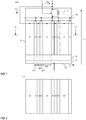
- FIG. 1 schematically illustrates a sectional view of one section of a superjunction transistor device.
- the transistor device includes a semiconductor body 100, wherein the semiconductor body 100 may include a conventional semiconductor material such as, for example, silicon (Si), or silicon carbide (SiC).
- the transistor device in the semiconductor body 100, includes a drift region 20 with a plurality of first regions 21 of a first doping type (conductivity type) and a plurality of second regions 22, 23 of a second doping type (conductivity type) complementary to the first doping type.
- the first regions 21 and the second regions 22, 23 are arranged alternately in the semiconductor body 100, and a pn-junction is formed between each first region 21 and a corresponding adjoining second region 22, 23.
- the first regions 21 and the second regions 22, 23 are arranged alternately in a first lateral direction x of the semiconductor body 100.
- the second regions 22, 23 include two different types of second regions, wide regions 22 and narrow regions 23, wherein the wide regions 22 and the narrow regions 23 are arranged alternately. In each case, a wide region 22 and a neighboring narrow region 23 are separated by a respective first region 21.
- the transistor device with the wide regions 22 and the narrow regions 23 of the second doping type can be produced in an efficient way, which will be explained in detail herein further below.
- the wide regions 22 have a first width w22 and the narrow regions 23 have a second width w23 that is smaller than the first width w22.
- the first width w22 is at least 1.05 times the second width w23, w22 ⁇ 1.05*w23.
- the first width w22 is at least 1.1 times or at least 1.2 times the second width w23.
- the first width w22 is less than 5 times, less than 4, or less than 2 times the second width w23.
- each of the first regions 21 and the second regions 22, 23 extends in a vertical direction z of the semiconductor body, wherein the vertical direction z is essentially perpendicular to the first lateral direction x.
- a dimension of the first and second regions 21, 22, 23 in the vertical direction is, inter alia, dependent on a desired voltage blocking capability of the transistor device and is selected from between several 10 micrometers and several 100 micrometers, for example.
- the respective width w22, w23 of each of the second regions 22, 23 may vary along the vertical direction z, which may be due to the manufacturing process. Further, the widths w22 of individual wide regions 22 may slightly deviate from each other, and the widths w23 of individual wide regions 22 may slightly deviate from each other. Thus, according to one example, the width w22 of a single wide region 22 denotes the average width of this wide region, and the width w22 of the plurality of wide regions 22 denotes the average width of the average widths of the wide regions 22.
- the width w23 of a single narrow region 23 denotes the average width of this narrow region
- the width w23 of the plurality of narrow regions 23 denotes the average width of the average widths of the narrow regions 23.
- a width w21 of a single first region 21 denotes the average width of this first region
- the width w21 of the plurality of first regions 21 denotes the average width of the average widths of the first regions 21.
- the transistor device is implemented in such a way that, at each vertical position of the semiconductor body 100, an effective dopant dose of second type dopant atoms in the wide regions 22 deviates less than 10%, less than 5%, or less than 1% from an effective dopant dose of second type dopant atoms in the narrow regions 23.
- the "effective dopant dose" at a vertical position of a second region 22, 23 is the integral of the effective (net) doping concentration of the second region 22, 23 in a direction perpendicular to one of the pn-junctions formed between the second region 22, 23 and the neighboring first region 21.
- the first and second regions 21, 22, 23 may be elongated in a second lateral direction y of the semiconductor body 100.
- This is illustrated in Figure 2 that shows a horizontal cross sectional view of the semiconductor body in a horizontal section plane A-A, which is a section plane perpendicular to the vertical section plane shown in Figure 1 .
- the second lateral direction y is essentially perpendicular to the first lateral direction x, according to one example.
- "Elongated" means that a length of the first and second regions 21, 22, 23 is significantly greater than the respective width w21, w22, w23.
- the width w21, w22, w23 is the dimension in the first lateral direction x and the "length" is the dimension in the second lateral direction y of the semiconductor body 100.
- "significantly greater” means that a ratio between the length and the width is greater than 10, greater than 100, or even greater than 1000.
- the first regions 21 are connected to a drain node D of the transistor device, and the second regions 22, 23 are connected to a source node S of the transistor device.
- a connection between the second regions 22, 23 and the source node S is only schematically illustrated in Figure 1 . Examples of how these connections can be implemented are explained with reference to examples herein further below.
- the first regions 21 are connected to the drain node D via a drain region 11 of the first doping type.
- the drain region 11 may adjoin the first regions 21. This, however, is not shown in Figure 1 .
- a buffer region 12 of the first doping type is arranged between the drain region 11 and the first regions 21.
- the buffer region 12 has the first doping type, which is the doping type of the drift regions 21 and the drain region 11.
- a doping concentration of the buffer region 12 is lower than a doping concentration of the drain region 11.
- the buffer region 12 includes two or more differently doped sub-regions (not shown).
- One of these sub-regions may have a doping concentration of between 1E14 cm -3 and 5E15 cm -3 , and another one of these sub-regions may have a doping concentration of between 5E15 cm -3 and 1E17 cm -3 .
- the transistor device further includes a control structure 3 connected between the source node S and the first regions 21.
- the control structure 3 is at least partially integrated in a semiconductor body 100. Examples of how the control structure 1 may be implemented are explained with reference to examples herein further below.
- the control structure furthermore includes a gate node G and is configured to control a conducting channel between the source node S and the first regions 21 dependent on a voltage V GS between the gate node G and the source node S.
- this function of the control structure 1 is represented by a switch connected between the source node S and the first regions 21.
- the control structure 1 includes a pn-junction between the first regions 21 and the source node S. In the example shown in Figure 1 , this pn-junction is represented by a bipolar diode connected between the first regions 21 and the source node S.
- the transistor device has a current flow direction, which is a direction in which a current may flow between the source node S and the drain node D inside the semiconductor body 100.
- the current flow direction corresponds to the vertical direction z of the semiconductor body 100, so that the drain region 11 is paced apart from the control structure 3 in the vertical direction.
- the vertical direction z is a direction perpendicular to a first surface (not shown in Figure 1 ) and a second surface 102 that is formed by the drain region 11.
- the "vertical cross sectional view" illustrated in Figure 1 is a sectional view in a section plane perpendicular to the first surface and the second surface 102 and parallel to the vertical direction z. Section planes perpendicular to the vertical section plane shown in Figure 1 are referred to as horizontal section planes.
- the transistor device can be operated in a forward biased state and a reverse biased state. Whether the device is in the forward biased state or the reverse biased state is dependent on a polarity of a drain-source voltage V DS , which is a voltage between the drain node D and the source node S.
- V DS drain-source voltage
- the polarity of the drain-source voltage V DS is such that the diode of the control structure 3 (which may also be referred to as body diode) is forward biased, so that in this operation state the transistor device conducts a current independent of an operation state of the control structure 3.
- the polarity of the drain-source V DS is such that the diode of the control structure 3 is reverse biased.
- the transistor device can be operated in an on-state or an off-state by the control structure 3.
- the control structure 3 In the on-state, the control structure 3 generates a conducting channel between the source node S and the first regions 21 so that a current can flow between the source node S and the drain node D via the control structure 3 and the first regions 21 of the first doping type.
- the conducting channel In the off-state the conducting channel is interrupted.
- space charge regions expand in the first regions 21 and the second regions 22, 23, so that the first regions 21 and the second regions 22, 23 may become depleted of charge carriers as the drain-source voltage V DS increases.
- charge carriers in the first regions 21 are "compensated" by charge carriers in the second regions 22, 23.
- the first regions 21 can be implemented with a higher doping concentration and, therefore, a lower resistance without decreasing the voltage blocking capability of the transistor device.
- drift region 20 and, therefore, a semiconductor device of the type shown in Figure 1 can be produced in an efficient way. Examples of a method for producing the drift region 20 are explained in the following.
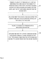
- Figure 3 illustrates a flow chart of a method according to one example.
- the method includes forming a plurality of trenches in at least one semiconductor layer, wherein each of the plurality of trenches has a first width, wherein the trenches are separated by mesa regions each having a second width, and wherein the first width is greater than the second width (201).
- the method further includes implanting first type dopant atoms and the second type dopant atoms into each of opposing sidewalls of the plurality of trenches (202), filling the plurality of trenches with a semiconductor material (203), and diffusing the first type dopant atoms and second type dopant atoms in a thermal process, so that first type dopant atoms form the first regions and second type dopant atoms form the second regions (204).
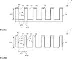
- FIGS 4A and 4B show a vertical cross sectional view of one section of a semiconductor layer 130 during the manufacturing process.
- This semiconductor layer 130 is also referred to as first semiconductor layer in the following.
- the first semiconductor layer 130 forms a portion of the semiconductor body 100 of the finished transistor device.
- further sections of the semiconductor body 100 such as the drain region 11 and the optional buffer region 12 may already have been formed. These further sections, however, are not illustrated in Figures 4A and 4B .
- the method includes forming a plurality of trenches 131 in a first surface 132 of the semiconductor layer 130 such that each of these trenches 131 extends, from the first surface 132 into the semiconductor layer 130.
- Forming the trenches 131 may include forming an etch mask 301 on top of the first surface 132, and etching those sections of the semiconductor layer 130 that are not covered by the etch mask 301.
- Etching the trenches includes using an anisotropic etching process, for example.
- Figure 4A shows the first semiconductor layer 130 after etching the trenches 131.
- the trenches 131 are elongated trenches. That is, a length of the trenches 131, which is the dimension of the trenches 131 in the second lateral direction y, is significantly greater than a width w131 of the trenches 131, which is a dimension of the trenches in the first lateral direction x.
- Each of the trenches 131 has a first sidewall 133 and an opposing second sidewall 134, wherein these sidewalls extend in the longitudinal direction (the second lateral direction y) of the trenches 131 and at least approximately extend in the vertical direction z.
- “At least approximately” means that the sidewalls 133, 134 are at least approximately perpendicular to the first surface 132. That is, the sidewalls 133, 134 can be perpendicular to the first surface 101 or can be tapered.
- a tapered sidewall is illustrated in dashed lines in Figure 4A .
- an angle (inside the first semiconductor layer 130) between each of the sidewalls 133, 134 and the first surface 132 is between 90° and 100°, in particular, between 92° and 95°.
- the trenches 131 are separated by mesa regions 135, so that each mesa region 135 is located between a respective pair of two neighboring trenches 131.
- Each of the mesa regions 135 has a width w135, which is a dimension of the respective mesa region 135 in the first lateral direction x.
- the width w131 of the trenches 131 is also referred to as first width in the following, and the width 135 of the mesa regions 135 is also referred to as second width in the following.
- the trenches 131 and, consequently, the mesa regions 135 can be tapered.
- the first width w131 of one trench denotes an average width of the respective trench 131
- the first width w131 of the plurality of trenches 131 denotes an average of the average widths of the trenches 131
- the width w135 of one mesa region 135 denotes an average width of the respective mesa region 135
- the width w135 of the plurality of mesa regions 135 denotes an average of the average widths of the mesa regions 135.
- the first width w131 is greater than the second width w135, w131 > w135.
- the first width 131 is at least 1.1 times, at least 1.2 times, or at least 1.5 times the second width w135, so that the trenches 131, in the first lateral direction x, are wider than the mesa regions 135.
- the first width w131 is less than three times the second width 135, w131 ⁇ 3*w135.
- the first width w131 is between 0.5 micrometers ( ⁇ m) and 6 micrometers, in particular between 1.5 micrometers and 3.5 micrometers.
- This pitch of the trench structure essentially equals a center distance between two neighboring narrow regions 23 or a center distance between two neighboring wide regions 22 in the finished superjunction transistor device.
- implementing the trenches 131 such that the first width w131 is greater than the second width w135 has the effect that deeper trenches can be formed as compared to a scenario in which the first width w131 equals the second width w135.
- the benefit of forming deeper trenches 131 is explained herein further below.
- the method further includes implanting first type dopant atoms and second type dopant atoms into each of the opposing first and second sidewalls 133, 134 in order to form implanted regions 24 in the mesa regions 135 along the sidewalls 133, 134 such that each of these implanted regions 24 includes both dopant atoms of the first doping type and dopant atoms of the second doping type.
- Forming the implanted regions 24 may include tilted implantation processes, wherein an implantation mask 401 formed on top of the mesa regions 135 may prevent dopant atoms from being implanted into the first surface 132.
- the implantation mask 401 is the etch mask 301.
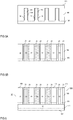
- Figure 5A shows the semiconductor layer 130 after filling the trenches 131 with a semiconductor material.
- Filling the trenches may include epitaxially growing a second semiconductor layer 140 on top of the first semiconductor layer 130 such that the trenches are completely filled.
- the second semiconductor layer 140 may be formed such that it fills the trenches and additionally covers the first surface 131 of the first semiconductor layer 130 on top of the mesa regions 135.
- filling the trenches include a planarization process in which a surface 141 of the second semiconductor layer 140 is planarized and/or in which a thickness of the second semiconductor layer 140 above the mesa regions 135 is reduced.
- the second semiconductor layer 140 is planarized or etched back down to the mesa regions 135, so that only sections of the second semiconductor layer 140 remain that fill the trenches 131.
- the semiconductor layer 140 is formed such that it at least fills the trenches 131 and, optionally, is also formed on top of the mesa regions 135.
- Epitaxially growing the second semiconductor layer 140 results in a monocrystalline layer arrangement including the first layer 130 and the second layer 140. In this arrangement, there is no visible boarder between the first and second layer 130, 140. Nevertheless, just for the purpose of illustration, the border between the two semiconductor layers 130, 140 are illustrated in dashed lines in Figure 5A .
- Figure 5B shows the layer arrangement shown in Figure 5A after a thermal process in which the first type dopant atoms and the second type dopant atoms included in the implanted regions 24 diffuse so that first type dopant atoms form the first regions 21 and second type dopant atoms form the second regions 22, 23.
- the first type dopant atoms and the second type dopant atoms are selected such that they have different diffusion coefficients, so that the annealing process results in the first regions 21 having an effective doping concentration of the first doping type and the second regions 22, 23 having an effective doping concentration of the second doping type.
- the first type dopant atoms have a lower diffusion coefficient than the second type dopant atoms, so that the first regions 21 form close to the position of the implanted regions 24 and, therefore, close to the positions of the first and second sidewalls 133, 134, while the second regions 22, 23 are spaced apart from the positions of the former sidewalls 133, 134.
- the first regions 21 include n-type dopant atoms and the second regions 22, 23 include p-type dopant atoms.
- the n-type dopant atoms include at least one of arsenic (As) atoms or antimony (Sb) atoms and the p-type dopant atoms include boron (B) atoms, so that The first type dopant atoms may include As atoms and/or Sb atoms and the second type dopant atoms may include B atoms.
- B atoms may diffuse up to four times faster than As atoms, for example.
- the first regions 21 may include dopant atoms of the second doping type.
- the dopant atoms of the first doping type prevail, resulting in an effective doping of the first dopant type.
- the second regions 22, 23 may include dopant atoms of the first doping type, wherein the dopant atoms of the second doping type prevail.
- the narrow regions 23 of the second doping type are those regions formed in the former mesa regions 135.
- the wide regions 22 are those regions formed in sections of the second layer 140 that fill the former trenches 131.
- the first semiconductor layer 130 and the second semiconductor layer 140 are essentially "non-doped" so that the number of first type dopant atoms and second type dopant atoms, essentially, is only defined by the implantation process.
- non-doped means that a basic doping concentration of each of the first and second semiconductor layers 130, 140 is less than 1E14 cm -3 or even less than 2E13 cm -3 .
- the drift region 20 may include only one first semiconductor layer 130 and one second semiconductor layer 140, which may also be referred to as top layer.
- a semiconductor body 100 with a drift region 20 of this type is illustrated in Figure 6 .
- Figure 6 illustrates the semiconductor body 100 of the superjunction transistor device after the annealing process and before forming the control structure 3.
- the semiconductor body 100 includes a carrier 110 that forms the drain region 11 and the optional buffer region 12, the first semiconductor layer 130 formed on top of the carrier 110, and the second semiconductor layer 140 formed on top of the first semiconductor layer 130.
- a surface 141 of the second semiconductor layer forms the surface 101 of the semiconductor body 100.
- the first semiconductor layer 130 is epitaxially grown on the carrier 110.
- the carrier may include a highly doped semiconductor substrate that forms the drain region 11 and, optionally, an epitaxial layer grown on the substrate that forms the buffer region 12.
- an arbitrary number of first semiconductor layers may be formed on the carrier one above the other, wherein in each of the first semiconductor layers trenches are formed and first and second type dopant atoms are implanted into opposing sidewalls of the trenches before a next one of the first semiconductor layers or the top layer is formed.
- Figure 7A The result of such process is illustrated in Figure 7A .
- Figure 7A shows one example of semiconductor body 100 that includes a carrier 110, a plurality of first semiconductor layers 130 1 , 130 n formed one above the other on top of the carrier 110, and a top layer 140 formed on an uppermost one 130 n of the first semiconductor layers 130 1 , 130 n .
- the carrier 110 includes the drain region 11 and the optional buffer region 12, according to one example.
- the plurality of first semiconductor layers 130 1 , 130 n further includes a lowermost layer 130 1 that is formed on top of the carrier 110.
- This lowermost semiconductor layer 130 1 has been processed in the same way as the semiconductor layer 130 explained with reference to Figures 4A and 4B . That is, a plurality of trenches were formed in the lowermost semiconductor layer 130 1 and implanted regions 24 have been formed in mesa regions along opposing sidewalls of the trenches.
- the plurality of first semiconductor layers 130 1 , 130 n further includes a further semiconductor layer 130 n .
- the further semiconductor layer 130 n is formed on the lowermost semiconductor layer 130 1 and fills the trenches in the lowermost semiconductor layer 130 1 .
- the further semiconductor layer 130 n has been processed in the same way as the semiconductor layer 130 shown in Figures 4A and 4B . That is, trenches were formed in this semiconductor layer 130 n and implanted regions 24 have been produced along opposing sidewalls of these trenches.
- the semiconductor body includes two first semiconductor layers 130 1 , 130 n , so that the further semiconductor layer 130 n forms the uppermost one of the first semiconductor layers 130 1 , 130 n on top of which the top layer 140 has been formed. It goes without saying that an arbitrary number of first semiconductor layers 130 1 , 130 n , in particular more than 2, more than 5, or more than 10 first semiconductor layers 130 1 -130 n of the same type as the semiconductor layers 130 1 , 130 n can be formed one above the other before forming the uppermost layer 140.
- Figure 7B shows the arrangement shown in Figure 7A after the annealing process.
- the annealing process results in a plurality of first regions 21 that continuously extend in the vertical direction z, and a plurality of second regions 22, 23 that continuously extend in the vertical direction z of the semiconductor body 100.
- the voltage blocking capability is greatly dependent on a length d20 of the drift region 20, wherein the length d20 is the dimension of the drift region 20 in the vertical direction z. Furthermore, a reduction of the pitch of the trench structure, which also results in a reduction of the pitch of the finished superjunction transistor device, may result in a reduction of the on-resistance of the transistor device. On the other hand, reducing the pitch of the trench structure has the effect that, at a given aspect ratio of the trenches, the trenches are produced with a smaller depth d131.
- pitch p the number of first semiconductor layers 130 that are to be produced in order to achieve a desired length d20 of the drift region 20 increases.
- Each additional semiconductor layer adds to the cost of the overall superjunction transistor device.
- forming the drift region 20 of the superjunction transistor device includes forming at least one first semiconductor layer 130, forming a plurality of trenches 131 in the at least one first semiconductor layer 130, forming implanted regions 24 in mesa regions along opposing sidewalls 134, 135 of the trenches 131, filling the trenches 131 with a semiconductor material, and an annealing process.
- the implanted regions 24 may be formed in various ways.
- implanting first type dopant atoms and second type dopant atoms into each of the first and second sidewalls 133, 134 includes implanting molecules that include both first type dopant atoms and second type dopant atoms, into the first sidewalls 133 in a first implantation process and into the second sidewalls 134 in a second implantation process.
- the method includes implanting the first type dopant atoms and the second type dopant atoms into one sidewall in separate implantation processes.
- this may include implanting first type dopant atoms into the first sidewalls 133 in a first implantation process, implanting first type dopant atoms into the second sidewalls 134 in a second implantation process, as illustrated in Figure 8A , implanting second type dopant atoms into the first sidewalls 133 in a third implantation process, and implanting the second type dopant atoms into the second sidewalls 134 in a fourth implantation process, as illustrated in Figure 8B .
- Figures 10A - 10C illustrates one example of doping concentrations of first type dopant atoms and second dopant atoms in horizontal layers of the drift region 20 after the annealing process ( Figure 10A ), the effective first type dopant charge in the first regions 21, and the effective second type dopant charge in the second regions 22, 23 after the annealing process ( Figure 10B ), and the electric field strength in the first regions 21 and the second regions 22, 23 in the off-state of the superjunction transistor device when a drain-source voltage V DS is applied.
- the "effective dopant charge” is the integral of the effective doping concentration in vertical planes that are parallel to the pn-junctions formed between the first and second regions 21, 22, 23.
- the transistor device includes wide second regions 22 and narrow second regions 23, the maximum field strength in the individual semiconductor regions 21, 22, 23 is essentially the same. This is highly desirable because this ensures that the voltage blocking capability is essentially the same for pn-junctions formed between first regions 21 and narrow second regions 22, and for pn-junctions formed between first regions 21 and wide second regions 23.
- This is basically achieved by controlling the annealing process such that an overall number of dopant atoms in the narrow regions 23 essentially equals the overall number of dopant atoms in the wide regions 23.
- the overall number of dopant atoms is essentially given by the integral of the dopant charge.
- a balancing of the number of dopant atoms in the narrow regions 23 and the wide regions 22 can be achieved by suitably selecting, for example, the duration and the temperature of the annealing process.
- the temperature is selected from between 1050 °C and 1100 °C and the duration is selected from between 250 minutes and 1000 minutes.
- the duration may be selected dependent on the pitch of the former trench structure, wherein the larger the pitch the longer the diffusion.
- the carrier 110 may include a semiconductor substrate.
- This substrate may include oxygen and/or COPs (Crystal Oriented Particles) which may diffuse into the at least one semiconductor layer 130.
- Oxygen and/or COP diffusing into the at least one semiconductor layer 130 may affect the diffusion of the first type and second type dopant atoms.
- the conditions (temperature, duration, ...) of the temperature process are selected dependent on a concentration of oxygen and/or COPs in the substrate.
- the process of forming the second regions 22, 23 such that each of these regions (in the same horizontal layer) essentially has the same number of dopant atoms can be supported by implanting the faster diffusing second type dopant atoms deeper into the first and second sidewalls 133, 134 than the slower diffusion first type dopant atoms.
- This is illustrated in Figure 11 , which illustrates the concentration of the first type dopant atoms and the second type dopant atoms in the mesa region 135 after the implantation process and after the diffusion process.
- the implantation depth of the first and second type dopant atoms can be adjusted by suitably adjusting the implantation energy.
- control structure 3 which is only schematically illustrated in Figure 1 , may be implemented in various ways. Some examples are explained in the following.
- the control structure is formed in the semiconductor body 100 after forming the top layer 140 and is at least partially formed in the top layer.
- the control structure may be formed after the annealing process that forms the first and second regions 21, 22, 23.
- the control structure 3 is at least partially formed before the annealing process, so that the same annealing process may be used to diffuse and activate dopant atoms of the first and second regions 21, 22, 23 and dopant atoms of doped regions in the control structure.
- Figure 12 shows one example of the control structure 3 in a greater detail. Besides the control structure 3, portions of the drift region 20 adjoining the control structure 3 are shown in Figure 12 .
- the control structure 3 includes a plurality of control cells 30, which may also be referred to as transistor cells.
- Each of these control cells 30 includes a body region 31 of the second doping type, a source region 32 of the first doping type, a gate electrode 33, and a gate dielectric 34.
- the gate dielectric 34 dielectrically insulates that gate electrode 33 from the body region 31.
- the body region 31 of each control cell 30 separates the respective source region 32 of the control cell 30 from at least one of the plurality of first regions 21.
- the source region 32 and the body region 31 of each of the plurality of control cells 30 is electrically connected to the source node S.
- Electrically connected in this context means ohmically connected. That is, there is no rectifying junction between the source node S and the source region 32 and the body region 31. Electrical connections between the source node S and the source region 32 and the body region 31 of the individual control cells 30 are only schematically illustrated in Figure 2 .
- the gate electrode 33 of each control cell 30 is electrically connected to the gate node G.
- the body region 31 of each control cell 30 adjoins at least one first region 21.
- the body region 31 is of the second doping type and the first region 21 is of the first doping type there is a pn-junction between the body region 31 of each control cell 30 and the at least one first region 21.
- These pn-junctions form a portion of the pn-junction of the control structure 3 that is represented by the bipolar diode in the equivalent circuit diagram of the control structure 3 shown in Figure 1 .
- the gate electrode 33 of each control structure 30 is a planar electrode arranged on top of the first surface 101 of the semiconductor body 100 and dielectrically insulated from the semiconductor body 100 by the gate dielectric 34. In this example, sections of the first regions 21, adjacent the individual body regions 31, extend to the first surface 101.
- FIG 13 shows a control structure 3 according to another example.
- the control structure 3 shown in Figure 3 is different from the control structure 3 shown in Figure 2 in that the gate electrode 33 of each control cell 30 is a trench electrode.
- This gate electrode 33 is arranged in a trench that extends from the first surface 101 into the semiconductor body 100.
- a gate dielectric 34 dielectrically insulates the gate electrode 33 from the respective body region 31.
- the body region 31 and the source region 32 of each control cell 30 are electrically connected to the source node S. Further, the body region 31 adjoins at least one first region 21 and forms a pn-junction with the respective first region 21.
- the control structures 30 each include one gate electrode 33, wherein the gate electrode 33 of each control cell 30 is configured to control a conducting channel between the source region 32 of the respective control cell 30 and one first region 21, so that each control cell 30 is associated with one first region 21.
- the body region 31 of each control cell 30 adjoins at least one second region 22, 23, so that the at least one second region 22, 23 is electrically connected to the source node S via the body region 31 of the control cell 30.
- the body region 31 of each control cell 30 adjoins one second region 22, 23 so that each control cell 30 is associated with one second region.
- the source regions 32 of two (or more) neighboring control cells 30 are formed by one doped region of the first doping type
- the body regions 31 of two (or more) neighboring control cells 30 are formed by one doped region of the second doping type
- the gate electrodes 33 of two (or more) control cells 30 are formed by one electrode.
- the gate electrodes 33 may include doped polysilicon, a metal, or the like.
- a doping concentration of the source regions 32 is selected from a range of between 1E18 cm -3 and 1E21 cm -3
- a doping concentration of the body regions 31 is selected from a range of between 1E16 cm -3 and 5E18 cm -3 .
- control cell 30 of the plurality of control cells Associating one control cell 30 of the plurality of control cells with one first region 21 and one second region 22, as illustrated in Figures 12 and 13 , is only an example.
- the implementation and the arrangement of the control cells 30 of the control structure 3 are widely independent of the specific implementation and arrangement of the first regions 21 and the second regions 22, 23.
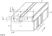
- FIG. 14 One example illustrating that the implementation and arrangement of the control structure 3 are widely independent of the implementation and arrangement of the first and second regions 21, 22 is shown in Figure 14 .
- the first regions 21 and the second regions 22 are elongated in the second lateral direction y of the semiconductor body 100, while the source regions 32, the body regions 31, and the gate electrodes 33 of the individual control cells 30 of the control structure 3 are elongated in the first lateral direction x perpendicular to the second lateral direction y.
- the body region 31 of one control cell 30 adjoins a plurality of first regions 21 and second regions 22.
- the transistor device can be implemented as an n-type transistor device or as a p-type transistor device.
- the first doping type which is the doping type of the first regions 21, the source regions 32, the drain region 11 and the optional buffer region 12 is an n-type
- the second doping type which is the doping type of the second regions 22, 23 and the body regions 31, is a p-type.
- the doping types of the device regions mentioned before are complementary to the doping types of the respective device regions in an n-type transistor device.
Landscapes
- Chemical & Material Sciences (AREA)
- Junction Field-Effect Transistors (AREA)
- Composite Materials (AREA)
- Crystallography & Structural Chemistry (AREA)
- Recrystallisation Techniques (AREA)
Abstract
Description
- This disclosure in general relates to a superjunction transistor device and a method for forming a superjunction transistor device, in particular, for forming a drift region of a superjunction transistor device.
- A superjunction device includes a drift region with at least one first region of a first doping type (conductivity type) and at least one second region of a second doping type (conductivity type) complementary to the first doping type. In some publications, the at least one first doping type region is referred to as drift region and the at least one second doping type region is referred to as compensation region.
- The drift region of a superjunction device may include a plurality of first regions and second regions which are alternatingly arranged in a semiconductor body. There is a need for forming such drift region in a cost efficient way.
- One example relates to a method. The method includes forming a plurality of first regions of a first doping type and a plurality of second regions of a second type in a semiconductor body such that the first regions and the second regions are arranged alternatingly in the semiconductor body. In this method, forming the first regions and the second regions includes forming a plurality of trenches in at least one semiconductor layer, implanting first type dopant atoms and second type dopant atoms into each of opposing sidewalls of the plurality of trenches, filling the plurality of trenches with a semiconductor material, and diffusing the first type dopant atoms and second type dopant atoms in a thermal process so that the first type dopant atoms form the first regions and the second type dopant atoms form the second regions. Each of the plurality of trenches has a first width and the trenches are separated by mesa regions each having a second width, wherein the first width is greater than the second width.
- Another example relates to a superjunction transistor device. The transistor device includes a drift region with a plurality of first regions of a first doping type and a plurality of second regions of a second type in a semiconductor body, wherein the first regions and the second regions are arranged alternatingly in the semiconductor body. The second regions include wide regions having a first width and narrow regions having a second width, wherein the wide regions and the narrow regions are arranged alternatingly, and wherein the first width is at least 1.05 times the second width.
- Examples are explained below with reference to the drawings. The drawings serve to illustrate certain principles, so that only aspects necessary for understanding these principles are illustrated. The drawings are not to scale. In the drawings the same reference characters denote like features.
-
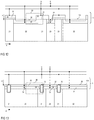
Figure 1 shows a vertical cross sectional view of a superjunction transistor device according to one example; -
Figure 2 shows a horizontal cross sectional view of one example of a drift region of the superjunction transistor device; -
Figure 3 shows a flowchart of one example of a method for forming the drift region; -
Figures 4A and 4B show a vertical cross sectional view of a first semiconductor layer during different process steps of a method for forming the drift region; -
Figures 5A and 5B illustrate the first layer shown inFigures 4A and 4B after further process steps that include forming a top layer; -
Figure 6 illustrates one example of a semiconductor body that includes one first semiconductor layer and a top layer; -
Figures 7A and 7B illustrate an example of a semiconductor body that includes several first semiconductor layers and a top layer; -
Figure 8 illustrates one example of a method for implanting first type dopant atoms and second type dopant atoms into sidewalls of trenches in the first semiconductor layer; -
Figures 9A and 9B illustrates another example of a method for implanting first type dopant atoms and second type dopant atoms into sidewalls of trenches in the first semiconductor layer; -
Figures 10A - 10C illustrates doping profiles of first and second semiconductor regions of a drift region and an associated electric field in blocking state of the transistor device; -
Figure 11 illustrates doping profiles of first and second semiconductor regions according to another example; -
Figure 12 shows one example of a control structure of the transistor device shown inFigure 1 ; -
Figure 13 shows another example of a control structure of the transistor device shown inFigure 1 ; and -
Figure 14 shows a perspective sectional view of a superjunction transistor device according to another example. - In the following detailed description, reference is made to the accompanying drawings. The drawings form a part of the description and for the purpose of illustration show examples of how the invention may be used and implemented. It is to be understood that the features of the various embodiments described herein may be combined with each other, unless specifically noted otherwise.
-
Figure 1 schematically illustrates a sectional view of one section of a superjunction transistor device. The transistor device includes asemiconductor body 100, wherein thesemiconductor body 100 may include a conventional semiconductor material such as, for example, silicon (Si), or silicon carbide (SiC). The transistor device, in thesemiconductor body 100, includes adrift region 20 with a plurality offirst regions 21 of a first doping type (conductivity type) and a plurality ofsecond regions first regions 21 and thesecond regions semiconductor body 100, and a pn-junction is formed between eachfirst region 21 and a corresponding adjoiningsecond region Figure 1 , thefirst regions 21 and thesecond regions semiconductor body 100. - Referring to
Figure 1 , thesecond regions wide regions 22 andnarrow regions 23, wherein thewide regions 22 and thenarrow regions 23 are arranged alternately. In each case, awide region 22 and a neighboringnarrow region 23 are separated by a respectivefirst region 21. The transistor device with thewide regions 22 and thenarrow regions 23 of the second doping type can be produced in an efficient way, which will be explained in detail herein further below. - The
wide regions 22 have a first width w22 and thenarrow regions 23 have a second width w23 that is smaller than the first width w22. According to one example, the first width w22 is at least 1.05 times the second width w23, w22 ≥ 1.05*w23. According to one example, the first width w22 is at least 1.1 times or at least 1.2 times the second width w23. According to one example, the first width w22 is less than 5 times, less than 4, or less than 2 times the second width w23. - Referring to
Figure 1 , each of thefirst regions 21 and thesecond regions second regions - The respective width w22, w23 of each of the
second regions wide regions 22 may slightly deviate from each other, and the widths w23 of individualwide regions 22 may slightly deviate from each other. Thus, according to one example, the width w22 of a singlewide region 22 denotes the average width of this wide region, and the width w22 of the plurality ofwide regions 22 denotes the average width of the average widths of thewide regions 22. Equivalently, the width w23 of a singlenarrow region 23 denotes the average width of this narrow region, and the width w23 of the plurality ofnarrow regions 23 denotes the average width of the average widths of thenarrow regions 23. Consequently, a width w21 of a singlefirst region 21 denotes the average width of this first region, and the width w21 of the plurality offirst regions 21 denotes the average width of the average widths of thefirst regions 21. - According to one example, the transistor device is implemented in such a way that, at each vertical position of the
semiconductor body 100, an effective dopant dose of second type dopant atoms in thewide regions 22 deviates less than 10%, less than 5%, or less than 1% from an effective dopant dose of second type dopant atoms in thenarrow regions 23. The "effective dopant dose" at a vertical position of asecond region second region second region first region 21. - The first and
second regions semiconductor body 100. This is illustrated inFigure 2 that shows a horizontal cross sectional view of the semiconductor body in a horizontal section plane A-A, which is a section plane perpendicular to the vertical section plane shown inFigure 1 . The second lateral direction y is essentially perpendicular to the first lateral direction x, according to one example. "Elongated" means that a length of the first andsecond regions Figures 1 and 2 , the width w21, w22, w23 is the dimension in the first lateral direction x and the "length" is the dimension in the second lateral direction y of thesemiconductor body 100. According to one example, "significantly greater" means that a ratio between the length and the width is greater than 10, greater than 100, or even greater than 1000. - Referring to
Figure 1 , thefirst regions 21 are connected to a drain node D of the transistor device, and thesecond regions second regions Figure 1 . Examples of how these connections can be implemented are explained with reference to examples herein further below. Thefirst regions 21 are connected to the drain node D via adrain region 11 of the first doping type. The drainregion 11 may adjoin thefirst regions 21. This, however, is not shown inFigure 1 . - Optionally, as shown in
Figure 1 , abuffer region 12 of the first doping type is arranged between thedrain region 11 and thefirst regions 21. Thebuffer region 12 has the first doping type, which is the doping type of thedrift regions 21 and thedrain region 11. According to one example, a doping concentration of thebuffer region 12 is lower than a doping concentration of thedrain region 11. The doping concentration of thedrain region 11 is selected from a range of between 1E17 (=1017) cm-3 and 1E20 cm-3, for example, and the doping concentration of thebuffer region 12 is selected from a range of between 1E14 cm-3 and 1E17 cm-3, for example. According to one example, thebuffer region 12 includes two or more differently doped sub-regions (not shown). One of these sub-regions may have a doping concentration of between 1E14 cm-3 and 5E15 cm-3, and another one of these sub-regions may have a doping concentration of between 5E15 cm-3 and 1E17 cm-3. - Referring to
Figure 1 , the transistor device further includes acontrol structure 3 connected between the source node S and thefirst regions 21. Thecontrol structure 3 is at least partially integrated in asemiconductor body 100. Examples of how the control structure 1 may be implemented are explained with reference to examples herein further below. The control structure furthermore includes a gate node G and is configured to control a conducting channel between the source node S and thefirst regions 21 dependent on a voltage VGS between the gate node G and the source node S. In the example shown inFigure 1 , this function of the control structure 1 is represented by a switch connected between the source node S and thefirst regions 21. Furthermore, the control structure 1 includes a pn-junction between thefirst regions 21 and the source node S. In the example shown inFigure 1 , this pn-junction is represented by a bipolar diode connected between thefirst regions 21 and the source node S. - The transistor device has a current flow direction, which is a direction in which a current may flow between the source node S and the drain node D inside the
semiconductor body 100. In the example shown inFigure 1 , the current flow direction corresponds to the vertical direction z of thesemiconductor body 100, so that thedrain region 11 is paced apart from thecontrol structure 3 in the vertical direction. The vertical direction z is a direction perpendicular to a first surface (not shown inFigure 1 ) and asecond surface 102 that is formed by thedrain region 11. The "vertical cross sectional view" illustrated inFigure 1 is a sectional view in a section plane perpendicular to the first surface and thesecond surface 102 and parallel to the vertical direction z. Section planes perpendicular to the vertical section plane shown inFigure 1 are referred to as horizontal section planes. - The transistor device can be operated in a forward biased state and a reverse biased state. Whether the device is in the forward biased state or the reverse biased state is dependent on a polarity of a drain-source voltage VDS, which is a voltage between the drain node D and the source node S. In the reverse biased state the polarity of the drain-source voltage VDS is such that the diode of the control structure 3 (which may also be referred to as body diode) is forward biased, so that in this operation state the transistor device conducts a current independent of an operation state of the
control structure 3. In the forward biased state, the polarity of the drain-source VDS is such that the diode of thecontrol structure 3 is reverse biased. In this forward biased state, the transistor device can be operated in an on-state or an off-state by thecontrol structure 3. In the on-state, thecontrol structure 3 generates a conducting channel between the source node S and thefirst regions 21 so that a current can flow between the source node S and the drain node D via thecontrol structure 3 and thefirst regions 21 of the first doping type. In the off-state the conducting channel is interrupted. - In the off-state, space charge regions (depletion regions) expand in the
first regions 21 and thesecond regions first regions 21 and thesecond regions first regions 21 are "compensated" by charge carriers in thesecond regions first regions 21 can be implemented with a higher doping concentration and, therefore, a lower resistance without decreasing the voltage blocking capability of the transistor device. - Referring to the above, a
drift region 20 and, therefore, a semiconductor device of the type shown inFigure 1 can be produced in an efficient way. Examples of a method for producing thedrift region 20 are explained in the following. -
Figure 3 illustrates a flow chart of a method according to one example. Referring toFigure 3 , the method includes forming a plurality of trenches in at least one semiconductor layer, wherein each of the plurality of trenches has a first width, wherein the trenches are separated by mesa regions each having a second width, and wherein the first width is greater than the second width (201). The method further includes implanting first type dopant atoms and the second type dopant atoms into each of opposing sidewalls of the plurality of trenches (202), filling the plurality of trenches with a semiconductor material (203), and diffusing the first type dopant atoms and second type dopant atoms in a thermal process, so that first type dopant atoms form the first regions and second type dopant atoms form the second regions (204). - One example of forming the plurality of trenches and implanting the first type dopant atoms and second type dopant atoms into sidewalls of the trenches is illustrated in
Figures 4A and 4B . Each of these figures shows a vertical cross sectional view of one section of asemiconductor layer 130 during the manufacturing process. Thissemiconductor layer 130 is also referred to as first semiconductor layer in the following. Thefirst semiconductor layer 130 forms a portion of thesemiconductor body 100 of the finished transistor device. At the time of processing thefirst semiconductor layer 130 further sections of thesemiconductor body 100, such as thedrain region 11 and theoptional buffer region 12 may already have been formed. These further sections, however, are not illustrated inFigures 4A and 4B . - Referring to
Figure 4A , the method includes forming a plurality oftrenches 131 in afirst surface 132 of thesemiconductor layer 130 such that each of thesetrenches 131 extends, from thefirst surface 132 into thesemiconductor layer 130. Forming thetrenches 131 may include forming anetch mask 301 on top of thefirst surface 132, and etching those sections of thesemiconductor layer 130 that are not covered by theetch mask 301. Etching the trenches includes using an anisotropic etching process, for example.Figure 4A shows thefirst semiconductor layer 130 after etching thetrenches 131. - According to one example, the
trenches 131 are elongated trenches. That is, a length of thetrenches 131, which is the dimension of thetrenches 131 in the second lateral direction y, is significantly greater than a width w131 of thetrenches 131, which is a dimension of the trenches in the first lateral direction x. - Each of the
trenches 131 has afirst sidewall 133 and an opposingsecond sidewall 134, wherein these sidewalls extend in the longitudinal direction (the second lateral direction y) of thetrenches 131 and at least approximately extend in the vertical direction z. "At least approximately" means that thesidewalls first surface 132. That is, thesidewalls first surface 101 or can be tapered. A tapered sidewall is illustrated in dashed lines inFigure 4A . According to one example, an angle (inside the first semiconductor layer 130) between each of thesidewalls first surface 132 is between 90° and 100°, in particular, between 92° and 95°. - Referring to
Figure 4A , thetrenches 131 are separated bymesa regions 135, so that eachmesa region 135 is located between a respective pair of two neighboringtrenches 131. Each of themesa regions 135 has a width w135, which is a dimension of therespective mesa region 135 in the first lateral direction x. The width w131 of thetrenches 131 is also referred to as first width in the following, and thewidth 135 of themesa regions 135 is also referred to as second width in the following. Referring to the above, thetrenches 131 and, consequently, themesa regions 135 can be tapered. According to one example, the first width w131 of one trench denotes an average width of therespective trench 131, and the first width w131 of the plurality oftrenches 131 denotes an average of the average widths of thetrenches 131. Equivalently, the width w135 of onemesa region 135 denotes an average width of therespective mesa region 135, and the width w135 of the plurality ofmesa regions 135 denotes an average of the average widths of themesa regions 135. - The first width w131 is greater than the second width w135, w131 > w135. According to one example, the
first width 131 is at least 1.1 times, at least 1.2 times, or at least 1.5 times the second width w135, so that thetrenches 131, in the first lateral direction x, are wider than themesa regions 135. According to one example, the first width w131 is less than three times thesecond width 135, w131<3*w135. According to one example, the first width w131 is between 0.5 micrometers (µm) and 6 micrometers, in particular between 1.5 micrometers and 3.5 micrometers. - An aspect ratio a131 of the
trenches 131 is given by a ratio between a depth d131, which is the dimension of the trenches in the vertical direction z, and the first width w131,
trenches 131 with a high aspect ratio, the aspect ratio is usually limited by the process that fills thetrenches 131 with the semiconductor material. It may be desirable to produce the semiconductor material that fills thetrenches 131 as a monocrystalline layer without any defects, such as voids. The higher the aspect ratio, the more difficult it is to fill thetrenches 131 with a defect-free semiconductor material. Thus, according to one example, thetrenches 131 are formed such that their aspect ratio a131 is between 2:1 and 3:1. - A pitch p of the trench structure shown in
Figure 4A is given by the first width w131 plus the second width w135, that is, the pitch is defined by one of thetrenches 131 and anadjoining mesa region 135,
narrow regions 23 or a center distance between two neighboringwide regions 22 in the finished superjunction transistor device. - At a given pitch p of the trench structure and at a given aspect ratio a131 of the
trenches 131, implementing thetrenches 131 such that the first width w131 is greater than the second width w135 has the effect that deeper trenches can be formed as compared to a scenario in which the first width w131 equals the second width w135. The benefit of formingdeeper trenches 131 is explained herein further below. - Referring to
Figure 4B , the method further includes implanting first type dopant atoms and second type dopant atoms into each of the opposing first andsecond sidewalls regions 24 in themesa regions 135 along thesidewalls regions 24 includes both dopant atoms of the first doping type and dopant atoms of the second doping type. Forming the implantedregions 24 may include tilted implantation processes, wherein animplantation mask 401 formed on top of themesa regions 135 may prevent dopant atoms from being implanted into thefirst surface 132. According to one example, theimplantation mask 401 is theetch mask 301. - Filling the plurality of
trenches 131 with a semiconductor material and diffusing the first type dopant atoms and second type dopant atoms in accordance with process steps 202 and 203 (see,Figure 2 ) is explained with reference toFigures 5A and 5B . Each of these figures shows the structure shown inFigure 4B after further process steps. -
Figure 5A shows thesemiconductor layer 130 after filling thetrenches 131 with a semiconductor material. Filling the trenches may include epitaxially growing asecond semiconductor layer 140 on top of thefirst semiconductor layer 130 such that the trenches are completely filled. Referring toFigure 5A , thesecond semiconductor layer 140 may be formed such that it fills the trenches and additionally covers thefirst surface 131 of thefirst semiconductor layer 130 on top of themesa regions 135. Optionally, filling the trenches include a planarization process in which asurface 141 of thesecond semiconductor layer 140 is planarized and/or in which a thickness of thesecond semiconductor layer 140 above themesa regions 135 is reduced. According to one example (not illustrated), thesecond semiconductor layer 140 is planarized or etched back down to themesa regions 135, so that only sections of thesecond semiconductor layer 140 remain that fill thetrenches 131. Thus, thesemiconductor layer 140 is formed such that it at least fills thetrenches 131 and, optionally, is also formed on top of themesa regions 135. - Epitaxially growing the
second semiconductor layer 140 results in a monocrystalline layer arrangement including thefirst layer 130 and thesecond layer 140. In this arrangement, there is no visible boarder between the first andsecond layer semiconductor layers Figure 5A . -
Figure 5B shows the layer arrangement shown inFigure 5A after a thermal process in which the first type dopant atoms and the second type dopant atoms included in the implantedregions 24 diffuse so that first type dopant atoms form thefirst regions 21 and second type dopant atoms form thesecond regions first regions 21 having an effective doping concentration of the first doping type and thesecond regions Figure 5B , the first type dopant atoms have a lower diffusion coefficient than the second type dopant atoms, so that thefirst regions 21 form close to the position of the implantedregions 24 and, therefore, close to the positions of the first andsecond sidewalls second regions former sidewalls - According to one example, the
first regions 21 include n-type dopant atoms and thesecond regions - Due to the different diffusion coefficients a segregation of the first type dopant atoms and the second type dopant atoms occurs, resulting in the first regions having an effective doping (net doping) of the first doping type and the
second regions first regions 21 may include dopant atoms of the second doping type. However, in thefirst regions 21, the dopant atoms of the first doping type prevail, resulting in an effective doping of the first dopant type. Equivalently, in addition to the dopant atoms of the second doping type, thesecond regions - Referring to
Figure 5B , thenarrow regions 23 of the second doping type are those regions formed in theformer mesa regions 135. Thewide regions 22 are those regions formed in sections of thesecond layer 140 that fill theformer trenches 131. - It may be desirable to precisely adjust the number of first type dopant atoms and the number of second type dopant atoms that are included in the layer arrangement after the annealing process. According to one example, the
first semiconductor layer 130 and thesecond semiconductor layer 140 are essentially "non-doped" so that the number of first type dopant atoms and second type dopant atoms, essentially, is only defined by the implantation process. According to one example, non-doped means that a basic doping concentration of each of the first and second semiconductor layers 130, 140 is less than 1E14 cm-3 or even less than 2E13 cm-3. - After the annealing process, the
first regions 21 and thesecond regions drift region 20 of the super junction transistor device. Thedrift region 20 may include only onefirst semiconductor layer 130 and onesecond semiconductor layer 140, which may also be referred to as top layer. Asemiconductor body 100 with adrift region 20 of this type is illustrated inFigure 6 . -
Figure 6 illustrates thesemiconductor body 100 of the superjunction transistor device after the annealing process and before forming thecontrol structure 3. In this example, thesemiconductor body 100 includes acarrier 110 that forms thedrain region 11 and theoptional buffer region 12, thefirst semiconductor layer 130 formed on top of thecarrier 110, and thesecond semiconductor layer 140 formed on top of thefirst semiconductor layer 130. In this exempla, asurface 141 of the second semiconductor layer forms thesurface 101 of thesemiconductor body 100. According to one example, thefirst semiconductor layer 130 is epitaxially grown on thecarrier 110. The carrier may include a highly doped semiconductor substrate that forms thedrain region 11 and, optionally, an epitaxial layer grown on the substrate that forms thebuffer region 12. - Forming the
drift region 20 based on only onefirst semiconductor layer 130 and atop layer 140, wherein trenches are formed only in thefirst semiconductor layer 130 but not thetop layer 140 is only an example. Basically, an arbitrary number of first semiconductor layers may be formed on the carrier one above the other, wherein in each of the first semiconductor layers trenches are formed and first and second type dopant atoms are implanted into opposing sidewalls of the trenches before a next one of the first semiconductor layers or the top layer is formed. The result of such process is illustrated inFigure 7A . -
Figure 7A shows one example ofsemiconductor body 100 that includes acarrier 110, a plurality of first semiconductor layers 1301, 130n formed one above the other on top of thecarrier 110, and atop layer 140 formed on anuppermost one 130n of the first semiconductor layers 1301, 130n. Thecarrier 110 includes thedrain region 11 and theoptional buffer region 12, according to one example. The plurality of first semiconductor layers 1301, 130n further includes alowermost layer 1301 that is formed on top of thecarrier 110. Thislowermost semiconductor layer 1301 has been processed in the same way as thesemiconductor layer 130 explained with reference toFigures 4A and 4B . That is, a plurality of trenches were formed in thelowermost semiconductor layer 1301 and implantedregions 24 have been formed in mesa regions along opposing sidewalls of the trenches. - The plurality of first semiconductor layers 1301, 130n further includes a
further semiconductor layer 130n. Thefurther semiconductor layer 130n is formed on thelowermost semiconductor layer 1301 and fills the trenches in thelowermost semiconductor layer 1301. Thefurther semiconductor layer 130n has been processed in the same way as thesemiconductor layer 130 shown inFigures 4A and 4B . That is, trenches were formed in thissemiconductor layer 130n and implantedregions 24 have been produced along opposing sidewalls of these trenches. - In the example shown in
Figure 7A , the semiconductor body includes two first semiconductor layers 1301, 130n, so that thefurther semiconductor layer 130n forms the uppermost one of the first semiconductor layers 1301, 130n on top of which thetop layer 140 has been formed. It goes without saying that an arbitrary number of first semiconductor layers 1301, 130n, in particular more than 2, more than 5, or more than 10 first semiconductor layers 1301-130n of the same type as the semiconductor layers 1301, 130n can be formed one above the other before forming theuppermost layer 140. -
Figure 7B shows the arrangement shown inFigure 7A after the annealing process. As can be seen fromFigure 7B , the annealing process results in a plurality offirst regions 21 that continuously extend in the vertical direction z, and a plurality ofsecond regions semiconductor body 100. - In a superjunction transistor device, the voltage blocking capability, is greatly dependent on a length d20 of the
drift region 20, wherein the length d20 is the dimension of thedrift region 20 in the vertical direction z. Furthermore, a reduction of the pitch of the trench structure, which also results in a reduction of the pitch of the finished superjunction transistor device, may result in a reduction of the on-resistance of the transistor device. On the other hand, reducing the pitch of the trench structure has the effect that, at a given aspect ratio of the trenches, the trenches are produced with a smaller depth d131. If, for example, the trench width w131 equals the mesa width w135 and the aspect ratio of thetrenches 131 is 2:1, the trench depth is essentially given by the pitch p of the trench structure (p=w131+w135). Thus, as the pitch p decreases, the number of first semiconductor layers 130 that are to be produced in order to achieve a desired length d20 of thedrift region 20 increases. Each additional semiconductor layer, however, adds to the cost of the overall superjunction transistor device. - At a given pitch p of the trench structure and a given aspect ratio a131 of the
trenches 131, producing thetrenches 131 such that their width w131 is greater than the width w134 of themesa regions 134 has the effect that, in order to achieve a desired length d20 of thedrift region 20, less first semiconductor layers are required as compared to a scenario in which w131=w134. Thus, the method explained herein before is suitable to produce thedrift region 20 of a superjunction transistor device in a very cost-efficient way. - Referring to the above, forming the
drift region 20 of the superjunction transistor device includes forming at least onefirst semiconductor layer 130, forming a plurality oftrenches 131 in the at least onefirst semiconductor layer 130, forming implantedregions 24 in mesa regions along opposingsidewalls trenches 131, filling thetrenches 131 with a semiconductor material, and an annealing process. The implantedregions 24 may be formed in various ways. - According to one example illustrated in
Figure 8 , implanting first type dopant atoms and second type dopant atoms into each of the first andsecond sidewalls first sidewalls 133 in a first implantation process and into thesecond sidewalls 134 in a second implantation process. - According to another example, the method includes implanting the first type dopant atoms and the second type dopant atoms into one sidewall in separate implantation processes. Referring to
Figures 8A and 8B this may include implanting first type dopant atoms into thefirst sidewalls 133 in a first implantation process, implanting first type dopant atoms into thesecond sidewalls 134 in a second implantation process, as illustrated inFigure 8A , implanting second type dopant atoms into thefirst sidewalls 133 in a third implantation process, and implanting the second type dopant atoms into thesecond sidewalls 134 in a fourth implantation process, as illustrated inFigure 8B . -
Figures 10A - 10C illustrates one example of doping concentrations of first type dopant atoms and second dopant atoms in horizontal layers of thedrift region 20 after the annealing process (Figure 10A ), the effective first type dopant charge in thefirst regions 21, and the effective second type dopant charge in thesecond regions Figure 10B ), and the electric field strength in thefirst regions 21 and thesecond regions second regions - In the example illustrated in
Figure 10 , although the transistor device includes widesecond regions 22 and narrowsecond regions 23, the maximum field strength in theindividual semiconductor regions first regions 21 and narrowsecond regions 22, and for pn-junctions formed betweenfirst regions 21 and widesecond regions 23. This is basically achieved by controlling the annealing process such that an overall number of dopant atoms in thenarrow regions 23 essentially equals the overall number of dopant atoms in thewide regions 23. The overall number of dopant atoms is essentially given by the integral of the dopant charge. According to one example, a balancing of the number of dopant atoms in thenarrow regions 23 and thewide regions 22 can be achieved by suitably selecting, for example, the duration and the temperature of the annealing process. According to one example, the temperature is selected from between 1050 °C and 1100 °C and the duration is selected from between 250 minutes and 1000 minutes. The duration, for example, may be selected dependent on the pitch of the former trench structure, wherein the larger the pitch the longer the diffusion. - Referring to the above, the
carrier 110 may include a semiconductor substrate. This substrate may include oxygen and/or COPs (Crystal Oriented Particles) which may diffuse into the at least onesemiconductor layer 130. Oxygen and/or COP diffusing into the at least onesemiconductor layer 130 may affect the diffusion of the first type and second type dopant atoms. Thus, according to one example, the conditions (temperature, duration, ...) of the temperature process are selected dependent on a concentration of oxygen and/or COPs in the substrate. - According to one example, the process of forming the
second regions second sidewalls Figure 11 , which illustrates the concentration of the first type dopant atoms and the second type dopant atoms in themesa region 135 after the implantation process and after the diffusion process. The implantation depth of the first and second type dopant atoms can be adjusted by suitably adjusting the implantation energy. - The
control structure 3, which is only schematically illustrated inFigure 1 , may be implemented in various ways. Some examples are explained in the following. In general, the control structure is formed in thesemiconductor body 100 after forming thetop layer 140 and is at least partially formed in the top layer. The control structure may be formed after the annealing process that forms the first andsecond regions control structure 3 is at least partially formed before the annealing process, so that the same annealing process may be used to diffuse and activate dopant atoms of the first andsecond regions -
Figure 12 shows one example of thecontrol structure 3 in a greater detail. Besides thecontrol structure 3, portions of thedrift region 20 adjoining thecontrol structure 3 are shown inFigure 12 . In the example shown inFigure 12 thecontrol structure 3 includes a plurality ofcontrol cells 30, which may also be referred to as transistor cells. Each of thesecontrol cells 30 includes abody region 31 of the second doping type, asource region 32 of the first doping type, agate electrode 33, and agate dielectric 34. Thegate dielectric 34 dielectrically insulates thatgate electrode 33 from thebody region 31. Thebody region 31 of eachcontrol cell 30 separates therespective source region 32 of thecontrol cell 30 from at least one of the plurality offirst regions 21. Thesource region 32 and thebody region 31 of each of the plurality ofcontrol cells 30 is electrically connected to the source node S. "Electrically connected" in this context means ohmically connected. That is, there is no rectifying junction between the source node S and thesource region 32 and thebody region 31. Electrical connections between the source node S and thesource region 32 and thebody region 31 of theindividual control cells 30 are only schematically illustrated inFigure 2 . Thegate electrode 33 of eachcontrol cell 30 is electrically connected to the gate node G. - Referring to the above, the
body region 31 of eachcontrol cell 30 adjoins at least onefirst region 21. As thebody region 31 is of the second doping type and thefirst region 21 is of the first doping type there is a pn-junction between thebody region 31 of eachcontrol cell 30 and the at least onefirst region 21. These pn-junctions form a portion of the pn-junction of thecontrol structure 3 that is represented by the bipolar diode in the equivalent circuit diagram of thecontrol structure 3 shown inFigure 1 . - In the example shown in
Figure 2 , thegate electrode 33 of eachcontrol structure 30 is a planar electrode arranged on top of thefirst surface 101 of thesemiconductor body 100 and dielectrically insulated from thesemiconductor body 100 by thegate dielectric 34. In this example, sections of thefirst regions 21, adjacent theindividual body regions 31, extend to thefirst surface 101. -
Figure 13 shows acontrol structure 3 according to another example. Thecontrol structure 3 shown inFigure 3 is different from thecontrol structure 3 shown inFigure 2 in that thegate electrode 33 of eachcontrol cell 30 is a trench electrode. Thisgate electrode 33 is arranged in a trench that extends from thefirst surface 101 into thesemiconductor body 100. Like in the example shown inFigure 2 , agate dielectric 34 dielectrically insulates thegate electrode 33 from therespective body region 31. Thebody region 31 and thesource region 32 of eachcontrol cell 30 are electrically connected to the source node S. Further, thebody region 31 adjoins at least onefirst region 21 and forms a pn-junction with the respectivefirst region 21. - In the examples shown in
Figures 12 and 13 , thecontrol structures 30 each include onegate electrode 33, wherein thegate electrode 33 of eachcontrol cell 30 is configured to control a conducting channel between thesource region 32 of therespective control cell 30 and onefirst region 21, so that eachcontrol cell 30 is associated with onefirst region 21. Further, as shown inFigures 12 and 13 , thebody region 31 of eachcontrol cell 30 adjoins at least onesecond region second region body region 31 of thecontrol cell 30. Just for the purpose of illustration, in the examples shown inFigures 2 and3 , thebody region 31 of eachcontrol cell 30 adjoins onesecond region control cell 30 is associated with one second region. Furthermore, in the examples, shown inFigures 2 and3 , thesource regions 32 of two (or more) neighboringcontrol cells 30 are formed by one doped region of the first doping type, thebody regions 31 of two (or more) neighboringcontrol cells 30 are formed by one doped region of the second doping type, and thegate electrodes 33 of two (or more)control cells 30 are formed by one electrode. Thegate electrodes 33 may include doped polysilicon, a metal, or the like. - According to one example, a doping concentration of the
source regions 32 is selected from a range of between 1E18 cm-3 and 1E21 cm-3, and a doping concentration of thebody regions 31 is selected from a range of between 1E16 cm-3 and 5E18 cm-3. - Associating one
control cell 30 of the plurality of control cells with onefirst region 21 and onesecond region 22, as illustrated inFigures 12 and 13 , is only an example. The implementation and the arrangement of thecontrol cells 30 of thecontrol structure 3 are widely independent of the specific implementation and arrangement of thefirst regions 21 and thesecond regions - One example illustrating that the implementation and arrangement of the
control structure 3 are widely independent of the implementation and arrangement of the first andsecond regions Figure 14 . In this example, thefirst regions 21 and thesecond regions 22 are elongated in the second lateral direction y of thesemiconductor body 100, while thesource regions 32, thebody regions 31, and thegate electrodes 33 of theindividual control cells 30 of thecontrol structure 3 are elongated in the first lateral direction x perpendicular to the second lateral direction y. In this example, thebody region 31 of onecontrol cell 30 adjoins a plurality offirst regions 21 andsecond regions 22. - The transistor device can be implemented as an n-type transistor device or as a p-type transistor device. In an n-type transistor device, the first doping type, which is the doping type of the
first regions 21, thesource regions 32, thedrain region 11 and theoptional buffer region 12 is an n-type and the second doping type, which is the doping type of thesecond regions body regions 31, is a p-type. In a p-type transistor device, the doping types of the device regions mentioned before are complementary to the doping types of the respective device regions in an n-type transistor device.
Claims (14)
- A method, comprising:forming a plurality of first regions (21) of a first doping type and a plurality of second regions (22, 23) of a second type in a semiconductor body (100) such that the first regions (21) and the second regions (22, 23) are arranged alternatingly in the semiconductor body (100),wherein forming the first regions (21) and the second regions (22, 23) comprises:forming a plurality of trenches (131) in at least one semiconductor layer (130);implanting first type dopant atoms and second type dopant atoms into each of opposing sidewalls (133, 134) of the plurality of trenches (131);filling the plurality of trenches (131) with a semiconductor material; anddiffusing the first type dopant atoms and second type dopant atoms in a thermal process so that first type dopant atoms form the first regions (21) and second type dopant atoms form the second regions (22, 23),wherein each of the plurality of trenches (131) has a first width (w131),wherein the trenches (131) are separated by mesa regions (135) each having a second width (w135), andwherein the first width (w131) is greater than the second width (w135).
- The method of claim 1,
wherein the first width (w131) is at least 1.05 times, at least 1.1 times, at least 1.2 times, or at least 1.5 times the second width (w135). - The method of claim 1 or 2, wherein the first width (w131) is less than 3 times the second width (w135).
- The method of any one of claims 1 to 3, wherein an aspect ratio of the trenches (131) is between 2:1 and 3:1.
- The method of any one of the preceding claims, wherein the second type dopant atoms are implanted deeper into the sidewalls (133, 134) than the first type dopant atoms.
- The method of any one of the preceding claims,
wherein the first type dopant atoms comprise at least one of arsenic (As) and antimony (Sb) atoms, and
wherein the second type dopant atoms comprise Boron (B) atoms. - The method of any one of the preceding claims, wherein an overall amount of first type dopants implanted into each of the sidewalls (133, 134) deviates less than 5%, less than 2%, or less than 1% from an overall amount of second type dopant atoms implanted into the respective sidewall.
- The method of any one of the preceding claims, wherein filling the trenches (131) comprises forming an epitaxial layer in the trenches (131) and on top of the mesa regions (135).
- The method of any one of the preceding claims, wherein forming a plurality of trenches (131) in at least one semiconductor layer (130) comprises:
forming a plurality of semiconductor layers (1301, 130n) one above the other and forming a plurality of trenches (131) in each of the plurality of semiconductor layers (1301, 130n) before forming a next one of the plurality of semiconductor layers (1301, 130n). - The method of any one of the preceding claims, further comprising:forming a control structure (3) with a plurality of source regions (32) of the first doping type and a plurality of body regions (31) of the second doping type such thateach of the first regions (21) adjoins at least one of the plurality of body regions (31) andeach of the second regions (22) adjoins at least one of the plurality of body regions (31).
- A superjunction transistor device comprising:a drift region with a plurality of first regions (21) of a first doping type and a plurality of second regions (22, 23) of a second type in a semiconductor body (100),wherein the first regions (21) and the second regions (22, 23) are arranged alternately in the semiconductor body (100),wherein the second regions (22, 23) comprise wide regions (22) having a first width (w22) and narrow regions (23) having a second width (w23),wherein the wide regions (22) and the narrow regions (23) are arranged alternately, andwherein the first width (w22) is at least 1.05 times the second width (w23).
- The superjunction transistor device of claim 11,
wherein the first width (w22) is at least 1.1 times, at least 1.2, or at least 2 times the second width (w23). - The superjunction transistor device of claim 11 or 12,
wherein the first width (w22) is less than 5 times, less than 4, or less than 2 times the second width (w23). - The superjunction transistor device of any one of claims 11 to 13,
wherein an effective dopant dose of second type dopant atoms in the wide regions (22) deviates less than 10%, less than 5%, or less than 1% from an effective dopant dose of second type dopant atoms in the narrow regions (23).
Priority Applications (3)
| Application Number | Priority Date | Filing Date | Title |
|---|---|---|---|
| CN202110575838.3A CN113745115B (en) | 2020-05-27 | 2021-05-26 | Superjunction transistor device and method for forming a superjunction transistor device |
| US17/330,562 US12034040B2 (en) | 2020-05-27 | 2021-05-26 | Superjunction transistor device and method for forming a superjunction transistor device |
| US18/734,605 US20240321953A1 (en) | 2020-05-27 | 2024-06-05 | Superjunction transistor device |
Applications Claiming Priority (1)
| Application Number | Priority Date | Filing Date | Title |
|---|---|---|---|
| EP20176749.8A EP3916761A1 (en) | 2020-05-27 | 2020-05-27 | Method for producing a superjunction device |
Publications (1)
| Publication Number | Publication Date |
|---|---|
| EP3916762A1 true EP3916762A1 (en) | 2021-12-01 |
Family
ID=70861284
Family Applications (2)
| Application Number | Title | Priority Date | Filing Date |
|---|---|---|---|
| EP20176749.8A Pending EP3916761A1 (en) | 2020-05-27 | 2020-05-27 | Method for producing a superjunction device |
| EP20188912.8A Pending EP3916762A1 (en) | 2020-05-27 | 2020-07-31 | Superjunction transistor device and method for forming a superjunction transistor device |
Family Applications Before (1)
| Application Number | Title | Priority Date | Filing Date |
|---|---|---|---|
| EP20176749.8A Pending EP3916761A1 (en) | 2020-05-27 | 2020-05-27 | Method for producing a superjunction device |
Country Status (3)
| Country | Link |
|---|---|
| US (3) | US11652138B2 (en) |
| EP (2) | EP3916761A1 (en) |
| CN (1) | CN113745115B (en) |
Families Citing this family (2)
| Publication number | Priority date | Publication date | Assignee | Title |
|---|---|---|---|---|
| US12684844B2 (en) | 2021-08-13 | 2026-07-14 | Infineon Technologies Austria Ag | Semiconductor device and method of producing thereof |
| US20260239676A1 (en) * | 2023-02-15 | 2026-08-13 | Infineon Technologies Austria Ag | Superjunction-JFET, Method for Producing a Superjunction-JFET and Electronic Circuit |
Citations (4)
| Publication number | Priority date | Publication date | Assignee | Title |
|---|---|---|---|---|
| DE102007026745A1 (en) * | 2007-06-06 | 2008-12-24 | Infineon Technologies Austria Ag | Semiconductor element comprises semiconductor body with drift section structure, where trench structure that has trench walls and trench body, is filled with vertically aligned semiconductor material |
| US20180374741A1 (en) * | 2017-06-22 | 2018-12-27 | Infineon Technologies Austria Ag | Method for Forming an Alignment Mark |
| US20190288061A1 (en) * | 2018-03-16 | 2019-09-19 | Infineon Technologies Austria Ag | Method for Forming a Superjunction Transistor Device |
| US20200176559A1 (en) * | 2018-11-30 | 2020-06-04 | Infineon Technologies Austria Ag | Method for Forming a Superjunction Transistor Device |
Family Cites Families (23)
| Publication number | Priority date | Publication date | Assignee | Title |
|---|---|---|---|---|
| DE19843959B4 (en) * | 1998-09-24 | 2004-02-12 | Infineon Technologies Ag | Method for producing a semiconductor component with a blocking pn junction |
| US6828204B2 (en) * | 2002-10-16 | 2004-12-07 | Varian Semiconductor Equipment Associates, Inc. | Method and system for compensating for anneal non-uniformities |
| DE102007004616B4 (en) * | 2006-01-31 | 2014-01-23 | Denso Corporation | A semiconductor device having a super junction structure and a method of manufacturing the same |
| JP2011051885A (en) | 2009-08-04 | 2011-03-17 | Sumitomo Chemical Co Ltd | Carbon material |
| JP2011054885A (en) * | 2009-09-04 | 2011-03-17 | Sony Corp | Semiconductor device, and method for manufacturing semiconductor device |
| JP5849882B2 (en) * | 2011-09-27 | 2016-02-03 | 株式会社デンソー | Semiconductor device provided with vertical semiconductor element |
| US8860136B2 (en) * | 2012-12-03 | 2014-10-14 | Infineon Technologies Ag | Semiconductor device and method of manufacturing a semiconductor device |
| US9515137B2 (en) * | 2013-02-21 | 2016-12-06 | Infineon Technologies Austria Ag | Super junction semiconductor device with a nominal breakdown voltage in a cell area |
| US9117694B2 (en) * | 2013-05-01 | 2015-08-25 | Infineon Technologies Austria Ag | Super junction structure semiconductor device based on a compensation structure including compensation layers and a fill structure |
| US9070580B2 (en) * | 2013-05-01 | 2015-06-30 | Infineon Technologies Austria Ag | Semiconductor device with a super junction structure based on a compensation structure with compensation layers and having a compensation rate gradient |
| US9024383B2 (en) * | 2013-05-01 | 2015-05-05 | Infineon Technologies Austria Ag | Semiconductor device with a super junction structure with one, two or more pairs of compensation layers |
| US9449968B2 (en) * | 2013-12-27 | 2016-09-20 | Infineon Technologies Austria Ag | Method for manufacturing a semiconductor device and a semiconductor device |
| EP2945192A1 (en) * | 2014-05-14 | 2015-11-18 | Nxp B.V. | Semiconductive device and associated method of manufacture |
| US9461109B1 (en) * | 2014-06-26 | 2016-10-04 | Icemos Technology, Ltd. | Method of forming superjunction high voltage devices using wafer bonding |
| DE102015115173A1 (en) * | 2015-09-09 | 2017-03-09 | Infineon Technologies Austria Ag | A semiconductor wafer, an implantation device for implanting protons, and a method of forming a semiconductor device |
| DE102015118616B3 (en) * | 2015-10-30 | 2017-04-13 | Infineon Technologies Austria Ag | Latchup-solid transistor |
| US9620585B1 (en) * | 2016-07-08 | 2017-04-11 | Semiconductor Components Industries, Llc | Termination for a stacked-gate super-junction MOSFET |
| DE102017115412A1 (en) * | 2016-07-14 | 2018-01-18 | Infineon Technologies Austria Ag | Process for producing a superconducting device |
| DE102016118499B4 (en) * | 2016-09-29 | 2023-03-30 | Infineon Technologies Dresden Gmbh | Semiconductor devices and method of forming a semiconductor device |
| US10861931B2 (en) * | 2016-12-08 | 2020-12-08 | Cree, Inc. | Power semiconductor devices having gate trenches and buried edge terminations and related methods |
| US10236342B2 (en) * | 2017-04-07 | 2019-03-19 | Semiconductor Components Industries, Llc | Electronic device including a termination structure |
| DE102017118957B4 (en) * | 2017-08-18 | 2021-10-21 | Infineon Technologies Austria Ag | MANUFACTURING A SUPERJUNCTION TRANSISTOR COMPONENT |
| US11056585B2 (en) * | 2018-04-20 | 2021-07-06 | Ipower Semiconductor | Small pitch super junction MOSFET structure and method |
-
2020
- 2020-05-27 EP EP20176749.8A patent/EP3916761A1/en active Pending
- 2020-07-31 EP EP20188912.8A patent/EP3916762A1/en active Pending
-
2021
- 2021-05-26 US US17/330,681 patent/US11652138B2/en active Active
- 2021-05-26 CN CN202110575838.3A patent/CN113745115B/en active Active
- 2021-05-26 US US17/330,562 patent/US12034040B2/en active Active
-
2024
- 2024-06-05 US US18/734,605 patent/US20240321953A1/en active Pending
Patent Citations (4)
| Publication number | Priority date | Publication date | Assignee | Title |
|---|---|---|---|---|
| DE102007026745A1 (en) * | 2007-06-06 | 2008-12-24 | Infineon Technologies Austria Ag | Semiconductor element comprises semiconductor body with drift section structure, where trench structure that has trench walls and trench body, is filled with vertically aligned semiconductor material |
| US20180374741A1 (en) * | 2017-06-22 | 2018-12-27 | Infineon Technologies Austria Ag | Method for Forming an Alignment Mark |
| US20190288061A1 (en) * | 2018-03-16 | 2019-09-19 | Infineon Technologies Austria Ag | Method for Forming a Superjunction Transistor Device |
| US20200176559A1 (en) * | 2018-11-30 | 2020-06-04 | Infineon Technologies Austria Ag | Method for Forming a Superjunction Transistor Device |
Also Published As
| Publication number | Publication date |
|---|---|
| CN113745115A (en) | 2021-12-03 |
| EP3916761A1 (en) | 2021-12-01 |
| US20210376064A1 (en) | 2021-12-02 |
| CN113745115B (en) | 2025-02-11 |
| US20210376063A1 (en) | 2021-12-02 |
| US11652138B2 (en) | 2023-05-16 |
| US20240321953A1 (en) | 2024-09-26 |
| US12034040B2 (en) | 2024-07-09 |
Similar Documents
| Publication | Publication Date | Title |
|---|---|---|
| US6979862B2 (en) | Trench MOSFET superjunction structure and method to manufacture | |
| US8772869B2 (en) | Power semiconductor device | |
| US8633095B2 (en) | Semiconductor device with voltage compensation structure | |
| US11342187B2 (en) | Method for producing a superjunction device | |
| US8519476B2 (en) | Method of forming a self-aligned charge balanced power DMOS | |
| US20240321953A1 (en) | Superjunction transistor device | |
| EP1009036A1 (en) | High-voltage MOS-gated power device, and related manufacturing process | |
| JP2004509452A (en) | Power metal oxide semiconductor field effect transistor and method of manufacturing the same | |
| EP1425802A2 (en) | Power mosfet having a trench gate electrode and method of making the same | |
| EP1487021A1 (en) | Semiconductor device | |
| US11929395B2 (en) | Superjunction transistor device | |
| US6969657B2 (en) | Superjunction device and method of manufacture therefor | |
| EP3955310A1 (en) | Method for producing a superjunction device | |
| US10553681B2 (en) | Forming a superjunction transistor device | |
| US11158705B2 (en) | Method for forming a superjunction transistor device | |
| US11527608B2 (en) | Method for producing a transistor device having a superjunction structure | |
| US20260082628A1 (en) | Semiconductor device including a trench gate structure | |
| EP3751598B1 (en) | Method for forming a superjunction transistor device | |
| EP4053910A1 (en) | Method of producing a transistor device | |
| CN120379289A (en) | Super junction MOSFET and preparation method thereof |
Legal Events
| Date | Code | Title | Description |
|---|---|---|---|
| PUAI | Public reference made under article 153(3) epc to a published international application that has entered the european phase |
Free format text: ORIGINAL CODE: 0009012 |
|
| STAA | Information on the status of an ep patent application or granted ep patent |
Free format text: STATUS: THE APPLICATION HAS BEEN PUBLISHED |
|
| AK | Designated contracting states |
Kind code of ref document: A1 Designated state(s): AL AT BE BG CH CY CZ DE DK EE ES FI FR GB GR HR HU IE IS IT LI LT LU LV MC MK MT NL NO PL PT RO RS SE SI SK SM TR |
|
| B565 | Issuance of search results under rule 164(2) epc |
Effective date: 20210122 |
|
| STAA | Information on the status of an ep patent application or granted ep patent |
Free format text: STATUS: REQUEST FOR EXAMINATION WAS MADE |
|
| 17P | Request for examination filed |
Effective date: 20220601 |
|
| RBV | Designated contracting states (corrected) |
Designated state(s): AL AT BE BG CH CY CZ DE DK EE ES FI FR GB GR HR HU IE IS IT LI LT LU LV MC MK MT NL NO PL PT RO RS SE SI SK SM TR |
|
| STAA | Information on the status of an ep patent application or granted ep patent |
Free format text: STATUS: EXAMINATION IS IN PROGRESS |
|
| 17Q | First examination report despatched |
Effective date: 20251218 |
|
| STAA | Information on the status of an ep patent application or granted ep patent |
Free format text: STATUS: THE APPLICATION IS DEEMED TO BE WITHDRAWN |