EP3916591A1 - Memory integrity performance enhancement systems and methods - Google Patents
Memory integrity performance enhancement systems and methods Download PDFInfo
- Publication number
- EP3916591A1 EP3916591A1 EP20206934.0A EP20206934A EP3916591A1 EP 3916591 A1 EP3916591 A1 EP 3916591A1 EP 20206934 A EP20206934 A EP 20206934A EP 3916591 A1 EP3916591 A1 EP 3916591A1
- Authority
- EP
- European Patent Office
- Prior art keywords
- data
- tier
- circuitry
- metadata
- line
- Prior art date
- Legal status (The legal status is an assumption and is not a legal conclusion. Google has not performed a legal analysis and makes no representation as to the accuracy of the status listed.)
- Granted
Links
Images




Classifications
-
- H—ELECTRICITY
- H04—ELECTRIC COMMUNICATION TECHNIQUE
- H04L—TRANSMISSION OF DIGITAL INFORMATION, e.g. TELEGRAPHIC COMMUNICATION
- H04L63/00—Network architectures or network communication protocols for network security
- H04L63/04—Network architectures or network communication protocols for network security for providing a confidential data exchange among entities communicating through data packet networks
-
- G—PHYSICS
- G06—COMPUTING OR CALCULATING; COUNTING
- G06F—ELECTRIC DIGITAL DATA PROCESSING
- G06F11/00—Error detection; Error correction; Monitoring
- G06F11/07—Responding to the occurrence of a fault, e.g. fault tolerance
- G06F11/08—Error detection or correction by redundancy in data representation, e.g. by using checking codes
- G06F11/10—Adding special bits or symbols to the coded information, e.g. parity check, casting out 9's or 11's
- G06F11/1076—Parity data used in redundant arrays of independent storages, e.g. in RAID systems
-
- G—PHYSICS
- G06—COMPUTING OR CALCULATING; COUNTING
- G06F—ELECTRIC DIGITAL DATA PROCESSING
- G06F3/00—Input arrangements for transferring data to be processed into a form capable of being handled by the computer; Output arrangements for transferring data from processing unit to output unit, e.g. interface arrangements
- G06F3/06—Digital input from, or digital output to, record carriers, e.g. RAID, emulated record carriers or networked record carriers
- G06F3/0601—Interfaces specially adapted for storage systems
- G06F3/0602—Interfaces specially adapted for storage systems specifically adapted to achieve a particular effect
- G06F3/0614—Improving the reliability of storage systems
- G06F3/0619—Improving the reliability of storage systems in relation to data integrity, e.g. data losses, bit errors
-
- G—PHYSICS
- G06—COMPUTING OR CALCULATING; COUNTING
- G06F—ELECTRIC DIGITAL DATA PROCESSING
- G06F11/00—Error detection; Error correction; Monitoring
- G06F11/07—Responding to the occurrence of a fault, e.g. fault tolerance
- G06F11/08—Error detection or correction by redundancy in data representation, e.g. by using checking codes
- G06F11/10—Adding special bits or symbols to the coded information, e.g. parity check, casting out 9's or 11's
- G06F11/1008—Adding special bits or symbols to the coded information, e.g. parity check, casting out 9's or 11's in individual solid state devices
- G06F11/1012—Adding special bits or symbols to the coded information, e.g. parity check, casting out 9's or 11's in individual solid state devices using codes or arrangements adapted for a specific type of error
-
- G—PHYSICS
- G06—COMPUTING OR CALCULATING; COUNTING
- G06F—ELECTRIC DIGITAL DATA PROCESSING
- G06F21/00—Security arrangements for protecting computers, components thereof, programs or data against unauthorised activity
- G06F21/10—Protecting distributed programs or content, e.g. vending or licensing of copyrighted material ; Digital rights management [DRM]
-
- G—PHYSICS
- G06—COMPUTING OR CALCULATING; COUNTING
- G06F—ELECTRIC DIGITAL DATA PROCESSING
- G06F21/00—Security arrangements for protecting computers, components thereof, programs or data against unauthorised activity
- G06F21/60—Protecting data
-
- G—PHYSICS
- G06—COMPUTING OR CALCULATING; COUNTING
- G06F—ELECTRIC DIGITAL DATA PROCESSING
- G06F21/00—Security arrangements for protecting computers, components thereof, programs or data against unauthorised activity
- G06F21/70—Protecting specific internal or peripheral components, in which the protection of a component leads to protection of the entire computer
- G06F21/78—Protecting specific internal or peripheral components, in which the protection of a component leads to protection of the entire computer to assure secure storage of data
-
- G—PHYSICS
- G06—COMPUTING OR CALCULATING; COUNTING
- G06F—ELECTRIC DIGITAL DATA PROCESSING
- G06F3/00—Input arrangements for transferring data to be processed into a form capable of being handled by the computer; Output arrangements for transferring data from processing unit to output unit, e.g. interface arrangements
- G06F3/06—Digital input from, or digital output to, record carriers, e.g. RAID, emulated record carriers or networked record carriers
- G06F3/0601—Interfaces specially adapted for storage systems
- G06F3/0628—Interfaces specially adapted for storage systems making use of a particular technique
- G06F3/0655—Vertical data movement, i.e. input-output transfer; data movement between one or more hosts and one or more storage devices
- G06F3/0658—Controller construction arrangements
-
- H—ELECTRICITY
- H04—ELECTRIC COMMUNICATION TECHNIQUE
- H04L—TRANSMISSION OF DIGITAL INFORMATION, e.g. TELEGRAPHIC COMMUNICATION
- H04L9/00—Cryptographic mechanisms or cryptographic arrangements for secret or secure communications; Network security protocols
- H04L9/32—Cryptographic mechanisms or cryptographic arrangements for secret or secure communications; Network security protocols including means for verifying the identity or authority of a user of the system or for message authentication, e.g. authorization, entity authentication, data integrity or data verification, non-repudiation, key authentication or verification of credentials
- H04L9/3236—Cryptographic mechanisms or cryptographic arrangements for secret or secure communications; Network security protocols including means for verifying the identity or authority of a user of the system or for message authentication, e.g. authorization, entity authentication, data integrity or data verification, non-repudiation, key authentication or verification of credentials using cryptographic hash functions
- H04L9/3242—Cryptographic mechanisms or cryptographic arrangements for secret or secure communications; Network security protocols including means for verifying the identity or authority of a user of the system or for message authentication, e.g. authorization, entity authentication, data integrity or data verification, non-repudiation, key authentication or verification of credentials using cryptographic hash functions involving keyed hash functions, e.g. message authentication codes [MACs], CBC-MAC or HMAC
-
- H—ELECTRICITY
- H04—ELECTRIC COMMUNICATION TECHNIQUE
- H04W—WIRELESS COMMUNICATION NETWORKS
- H04W12/00—Security arrangements; Authentication; Protecting privacy or anonymity
- H04W12/10—Integrity
Definitions
- the present disclosure relates to memory integrity, more specifically, this disclosure relates to error detection and correction systems having reduced overhead requirements.
- Cloud security providers use cryptographic isolation for the customer workloads running on their platform.
- Various cryptographic isolation methods have been implemented to meet these requirements for the cloud providers, such as Secure Memory Encryption (SME) and Secure Encrypted Virtualization (SEV).
- Memory integrity operates by associating a cryptographic message authentication code (MAC) with each data line in memory. The MAC is generated when data is written to memory and verified when the data is read from memory. If data was modified, either when resident in memory, the MAC will not match and result in the modification attack being detected (a security exception can then be signaled to notify software of the attack).
- Traditional integrity approaches can suffer from significant performance overheads as the MAC associated with each data line must be loaded on each access and verified/updated depending on the type of memory access. This additional access results in storage, performance, and bandwidth overheads.
- the systems and methods disclosed herein provide a memory integrity architecture that features full error correction capabilities and high-strength memory integrity without introducing the performance overheads of traditional memory integrity approaches.
- the systems and methods disclosed herein use extended Reed-Solomon codes to provide error correction code (ECC) that includes error detection data and error correction data.
- ECC error correction code
- the use of Reed-Solomon codes advantageously permits splitting the ECC into two tiers (hereinafter, "Tier I" and "Tier II”).
- Tier I data including at least the error detection data and message authentication code (MAC) data, is stored in memory circuitry at the same location as the associated data line, such that at least the error detection data and MAC data are read during each read operation on the data line.
- MAC message authentication code
- Tier I data may, at times, also include other data such as security-related metadata, and some or all of the error correction data.
- Tier II data includes error correction data and is stored in a separate or sequestered location in the memory circuitry. The Tier II error correction data is accessed when the memory controller circuitry detects an error in the data line.
- Tier I stores performance sensitive metadata (e.g ., the error detection and correction tier of ECC, MAC) and Tier II uses sequestered memory to store the metadata associated with a data line that is off the performance critical path (e.g., the error correction tier of ECC).
- System performance is enhanced by obviating the need to read the MAC data and both the error detection data and error correction data during each read operation - instead, the MAC data and the error detection data are read during each read operation and only when a data error occurs is the full error correction data read.
- a data storage system may include: memory circuitry; controller circuitry to, for each of a plurality of lines of data stored in memory circuitry: generate metadata that includes: data representative of a cryptographic message authentication code associated with the respective line of data; and data representative of an error code associated with the respective line of data, the error correction code including at least error detection data associated with the respective line of data and error correction data associated with the respective line of data; and apportion the metadata into a Tier I portion stored in a first location in the memory circuitry proximate the respective line of data in the memory circuitry and a Tier II portion stored in a second location in the memory circuitry remote from the respective line of data; wherein the Tier I portion includes at least the error detection data portion and the message authentication code portion associated with the respective line of data; and wherein the Tier II portion includes at least a portion of the error correction data portion associated with the respective line of data.
- a data storage method may include: generating, by controller circuitry, metadata for each respective one of a plurality of lines of data stored in memory circuitry the metadata including: data representative of a cryptographic message authentication code (MAC) associated with the respective line of data; and data representative of an error correction code (ECC) associated with the respective line of data, the error correction code including at least error detection data associated with the respective line of data and error correction data associated with the respective line of data; and apportioning, by the controller circuitry, the metadata into a Tier I portion stored in a first memory location in the memory circuitry proximate the respective line of data and a Tier II portion stored in a second location in the memory circuitry remote from the respective line of data; wherein the Tier I portion includes at least the error detection data portion and the message authentication code portion of the metadata associated with the respective line of data; and wherein the Tier II portion includes at least a portion of the error correction data portion of the metadata associated with the respective line of data.
- MAC cryptographic message authentication code
- ECC error correction code
- a non-transitory storage device that includes instructions.
- the instructions when executed by controller circuitry, cause the controller circuitry to: generate metadata for each respective one of a plurality of lines of data stored in memory circuitry the metadata including: data representative of a cryptographic message authentication code (MAC) associated with the respective line of data; and data representative of an error correction code (ECC) associated with the respective line of data, the error correction code including at least error detection data associated with the respective line of data and error correction data associated with the respective line of data; and apportion the metadata into a Tier I portion stored in a first memory location in the memory circuitry proximate the respective line of data and a Tier II portion stored in a second location in the memory circuitry remote from the respective line of data; wherein the Tier I portion includes at least the error detection data portion and the message authentication code portion of the metadata associated with the respective line of data; and wherein the Tier II portion includes at least a portion of the error correction data portion of the metadata associated with the respective line of data.
- MAC cryptographic message authentication code
- a data storage system may include: means for generating metadata for each respective one of a plurality of lines of data stored in memory circuitry the metadata including: data representative of a cryptographic message authentication code (MAC) associated with the respective line of data; and data representative of an error correction code (ECC) associated with the respective line of data, the error correction code including at least error detection data associated with the respective line of data and error correction data associated with the respective line of data; and means for apportioning the metadata into a Tier I portion stored in a first memory location in the memory circuitry proximate the respective line of data and a Tier II portion stored in a second location in the memory circuitry remote from the respective line of data; wherein the Tier I portion includes at least the error detection data portion and the message authentication code portion of the metadata associated with the respective line of data; and wherein the Tier II portion includes at least a portion of the error correction data portion of the metadata associated with the respective line of data.
- MAC cryptographic message authentication code
- ECC error correction code
- electromagnetic memory such as random access memory (RAM); dual data rate RAM (DDR-RAM); static RAM (SRAM); and dynamic RAM (DRAM)
- RAM random access memory
- DDR-RAM dual data rate RAM
- SRAM static RAM
- DRAM dynamic RAM
- MRAM magneto-resistive RAM
- STT-MRAM spin transfer torque MRAM
- ReRAM resistive RAM
- quantum storage devices molecular storage devices; and similar.
- ordinals such as first, second and third does not necessarily imply a ranked sense of order, but rather may only distinguish between multiple instances of an act or structure.
- FIG 1 is a block diagram of an illustrative system 100 that includes controller circuitry 110 and memory circuitry 120 that includes: Tier I memory circuitry 130 to store data lines 132A-132n and associated Tier I metadata 134A-134n; and Tier II memory circuitry 140 to store Tier II metadata 142A-142n associated with respective ones of the data lines 132A-132n, in accordance with at least one embodiment described herein.
- the system 100 also includes processor circuitry 150 to execute one or more applications that perform memory operations such as memory read and memory write operations.
- the Tier I metadata 134A-134n includes message authentication code (MAC) data 136A-136n, each associated with a respective one of the data lines 132A-132n.
- the Tier I metadata 134A-134n also includes at least a first portion of the error correction code (ECC) 138A 1 -138n 1 , each associated with a respective one of the data lines 132A-132n.
- ECC error correction code
- the first portion of the ECC 138A 1 -138n 1 includes the error detection data portion of the respective ECC 138A-138n.
- the first portion of the ECC 138A 1 -138n 1 includes the error detection data portion of the respective ECC 138A-138n and at least a portion of the error correction data portion of the respective ECC 138A-138n.
- the Tier II metadata 142A-142n includes a second portion of the error correction code (ECC) 138A 2 -138n 2 , each associated with a corresponding one of the data lines 132A-132n.
- the controller circuitry 110 may encrypt the data line 132A and generate message authentication code (MAC) data 136A that is associated with the data line 132A.
- the controller circuitry 110 may also generate an error correction code (ECC) 138A, such as a Reed-Solomon ECC, that includes error detection data and error correction data, both associated with data line 132A.
- ECC error correction code
- the controller circuitry 110 stores the data line 132A and the Tier I metadata 134A, including at least the MAC data 136A and the first portion of the ECC data 138A 1 in the Tier I memory circuitry 130.
- the controller circuitry 110 stores the Tier II metadata 142A, including the second portion of the ECC data 138A 2 in a sequestered Tier II memory circuitry 140 that is remote from the Tier I memory circuitry 130.
- the controller circuitry 110 may retrieve the data line 132A and the Tier I metadata 134A, including the MAC data 136A and the first portion of the ECC data 138A 1 , associated with the data line 132A.
- the controller circuitry 110 uses the error detection data included in the first portion of the ECC data 138A 1 to detect if errors exist in the retrieved data 132A. If no errors are detected, the controller circuitry 110 decrypts and verifies the retrieved data 132A using the MAC data 136A included in the Tier I metadata 134A. Once verified by the controller circuitry 110, the verified data line 132A is then passed to the processor circuitry 150.
- the controller circuitry 110 If the retrieved data 132A cannot be verified by the controller circuitry 110 using the MAC data 136A, the controller circuitry 110 returns null data and the processor circuitry 150 throws an exception. If the controller circuitry 110 detects an error in the retrieved data line 132A, the controller circuitry 110 retrieves, from the Tier II memory circuitry 140, the Tier II metadata 142A. The controller circuitry 110 uses the error correction data included in the second portion of the ECC data 138A2 to correct the data line 132A prior to decrypting and verifying the retrieved data 132A using the MAC data 136A included in the Tier I metadata 134A.
- each of the data lines 132A-132n may include one or more lines in cache memory circuitry operably coupled to the processor circuitry 150.
- each of the data lines 132A-132n may include one or more level 1 (LI) cache lines; one or more level 2 (L2) cache lines; one or more last level cache (LLC) lines; or combinations thereof.
- Each of the data lines 132A-132n may include any number of bytes.
- each of the data lines 132A-132n may have the same or different number of bytes.
- each of data lines 132A-132n may include: 32 bytes; 64 bytes; 128 bytes; or 256 bytes.
- the Tier I metadata 134A-134n includes the MAC data 136A-136n and the first portion of the ECC data 138A 1 -138n 1 .
- the Tier I metadata 134A-134n may include other data such as security data that includes but is not limited to: tag and state data, directory/poison data, and similar security related data.
- the Tier I metadata 134A-134n may include only the first portion of the ECC data 138A 1 -138n 1 .
- the Tier I metadata 134A-134n may include the first portion of the ECC data 138A 1 -138n 1 and at least some of the bits included in the second portion of the ECC data 138A 2 -138n 2 .
- the Tier I metadata 134A-134n may include the first portion of the ECC data 138A 1 -138n 1 and the second portion of the ECC data 138A 2 -138n 2 .
- the Tier I metadata 134A-134n may include any number of bits.
- the Tier I metadata 134A-134n may include: 64 bits; 96 bits; 128 bits; or 256 bits.
- the MAC data 136A-136n included in the Tier I metadata 134A-134n may include any number of bits.
- the MAC data 136A-136n may include: 30 bits or less; 40 bits or less; 50 bits or less; or 60 bits or less.
- the first portion of the ECC data 138A 1 -138n 1 includes error detection data.
- the first portion of the ECC data 138A 1 -138n 1 includes error detection data and at least a portion of the error correction data.
- the first portion of the ECC data 138A 1 -138n 1 may include any number of bits.
- the first portion of the ECC data 138A 1 -138n 1 may include: 32 bits, 64 bits, 96 bits, or 128 bits.
- the Tier I metadata 134A-134n may include the first portion of the ECC data 138A 1 -138n 1 and at least some of the bits included in the second portion of the ECC data 138A 2 -138n 2 .
- the Tier I metadata 134A-134n may include any number of bits from the second portion of the ECC data 138A 2 -138n 2 .
- the Tier I metadata 134A-134n may include: 8 bits, 16 bits, or 32 bits of the second portion of the ECC data 138A 2 -138n 2 .
- the Tier I metadata 134A-134n may include the first portion of the ECC data 138A 1 -138n 1 and the second portion of the ECC data 138A 2 -138n 2 .
- the Tier I metadata 134A-134n may include a total of: 64 bits, 96 bits, or 128 bits of ECC data included in the first portion of the ECC data 138A 1 -138n 1 and the second portion of the ECC data 138A 2 -138n 2 .
- the Tier II metadata 142A-142n includes all or a portion of the second portion of the ECC data 138A 2 -138n 2 .
- the second portion of the ECC data 138A 2 -138n 2 may include error correction data that includes any number of bits.
- the Tier II metadata 142A-142n may include: 8 bits, 16 bits, 32 bits, 64 bits, 96 bits, or 128 bits of error correction data included in the second portion of the ECC data 138A 2 -138n 2 .
- the controller circuitry 110 includes any number and/or combination of currently available and/or future developed electronic components, optical components, semiconductor device, and/or logic elements capable of performing memory access, error detection, error correction, and verification operations on data communicated to or from the memory circuitry 130.
- the controller circuitry 110 may include memory controller circuitry.
- the processor circuitry 150 may provide all or a portion of the controller circuitry 110.
- the memory circuitry 120 includes any number and/or combination of currently available and/or future developed electronic components, optical components, semiconductor device, and/or logic elements capable of storing information and/or data.
- the memory circuitry 120 may include volatile memory, non-volatile memory, or any combination thereof.
- the memory circuitry 120 may be communicatively coupled to processor circuitry 150 that includes one or more processor core circuits, each processor core circuit capable of contemporaneous execution of one or more threads.
- the memory circuitry 120 may include cache memory circuitry communicatively coupled to the processor circuitry.
- the memory circuitry 120 may include level 1 (LI) cache memory circuitry, level 2 (L2) cache memory circuitry, last level cache (LLC) circuitry, or any combination thereof.
- all or a portion of the cache memory circuitry 120 may include cache circuitry shared between a plurality of processor core circuits included in the processor circuitry 150.
- the processor circuitry 150 may include a general-purpose processor, such as a Core® i3, i5, i7, 2 Duo and Quad, Xeon®, Itanium®, Atom®, or Quark® microprocessor, available from Intel® (Intel Corporation, SANTA CLARA, CA), Alternatively, the processor circuitry 150 may include one or more processors from another manufacturer or supplier, such as Advanced Micro Devices (AMD®, Inc.), ARM Holdings® Ltd, MIPS®, etc.
- the processor circuitry 150 may include a special-purpose processor, such as, for example, a network or communication processor, compression engine, graphics processor, co-processor, embedded processor, or the like.
- the processor circuitry 150 may be implemented as a single semiconductor package or as a combination of stacked or otherwise interconnected semiconductor packages and/or dies.
- the processor circuitry 150 may be a part of and/or may be implemented on one or more substrates using any of a number of process technologies, such as, for example, BiCMOS, CMOS, or NMOS.
- FIG 2A is an illustrative metadata configuration 200A using a 10x4 DDR5 memory module, in accordance with at least one embodiment described herein.
- FIG 2B is another illustrative metadata configuration 200B using a 9x4 DDR5 memory module, in accordance with at least one embodiment described herein.
- FIG 2C is yet another illustrative metadata configuration 200C using a 5x8 DDR5 memory module, in accordance with at least one embodiment described herein.
- FIGS 2A, 2B , and 2C represent illustrative embodiments, and the general principles behind the systems and methods disclosed herein may be readily applied to other memory module configurations with similar impact on system performance as described herein.
- the 10x4 DDR5 memory module 200A includes 10 storage devices, with 8 storage devices 202A-202H dedicated to the storage of data and 2 storage devices 204A and 204B dedicated to the storage of ECC data 138.
- Each data storage device 202 and each ECC storage device 204 provides 4 bytes of data in each cycle with a 64 byte cache line requiring a total of 16 cycles to be read out of the 10x4 DDR5 memory module 200A.
- the 9x4 DDR5 memory module 200B includes 9 storage devices, with 8 storage devices 202A-202H dedicated to the storage of data and 1 storage device 204A dedicated to the storage of ECC data 138.
- Each data storage device 202 and each ECC storage device 204 provides 4 bytes of data in each cycle with a 64 byte cache line again requiring a total of 16 cycles to be read out of the 9x4 DDR5 memory module 200B.
- the 5x8 DDR5 memory module 200C includes 9 storage devices, with 4 storage devices 206A-206D dedicated to the storage of data and 1 storage device 208A dedicated to the storage of ECC data 138.
- Each data storage device 206 and each ECC storage device 208 provides 8 bytes of data in each cycle with a 128 byte cache line requiring a total of 16 cycles to be read out of the 5x8 DDR5 memory module 200C.
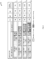
- FIG 3 is a table 300 providing a comparison of various metadata configurations 310, 320, 330, and 340, in accordance with at least one embodiment described herein.
- a base metadata configuration 310 in which all of the metadata, including a 64 bits of error detection + correction data, 32 bits of error correction data, 28 bits of MAC data and 4 bits of security (or other) data fit within the 128 bits allowable in the Tier I memory circuitry 130.
- the MAC data is limited to 28 bits and the security data is limited to 4 bits to fit within the 128 bit constraint of the Tier I memory circuitry 130.
- Configuration 320 provides a first metadata configuration in which the ECC data 138 is split into a first portion of ECC data 138 1 stored or otherwise retained in the Tier I memory circuitry 130 and a second portion of ECC data 138 2 stored or otherwise retained in the Tier II memory circuitry 140.
- the Tier I memory circuitry 130 stores or otherwise retains the first portion of the ECC data 138 1 (64 bits of error detection + partial error correction data), and a portion of the second portion of the ECC data 138 2 (16 bits of partial error correction data).
- the sequestered Tier II memory circuitry 140 stores or otherwise retains the remaining portion of the second portion of the ECC data 138 2 (16 bits of remaining error correction data).
- Tier I memory circuitry 130 is read on every memory read operation, thereby permitting error detection capabilities.
- the controller circuitry 110 accesses the second portion of the ECC data 138 2 (16 bits of remaining error correction data) in sequestered Tier II memory circuitry 140 only upon detecting an error.
- Tier I memory circuitry allocated to the storage of MAC data 136 has increased to 34 bits, providing an additional 6 bits of MAC data storage.
- Metadata configuration 320 beneficially provides increased capability for storage of other data - as depicted in configuration 320, up to 14 bits of other data.
- An example of such data includes but is not limited to tag bits used to support multi-level memory circuitry (e.g ., three-dimensional cross point memory circuitry "3DXP" memory circuitry as provided by Intel® Corp., SANTA CLARA, CA).
- Configuration 330 provides a second metadata configuration in which Tier I memory circuitry 130 contains the first portion of ECC data 138 1 (error detection + partial correction data) and Tier II memory circuitry 140 contains the second portion of ECC data 138 2 (remaining error correction data).
- the Tier I memory circuitry 130 stores the first portion of the ECC data 138 1 (64 bits of error detection + partial correction data), 50 bits of MAC data, and 14 bits of other data (multi-level memory tag and state, Directory/Poison and other security related metadata).
- the sequestered Tier II memory circuitry 140 stores the second portion of the ECC data 138 2 (32 bits of remaining error correction).
- Tier I memory circuitry 130 including the first portion of the ECC data 138 1 , containing the error detection data, is read on every memory read operation, thereby permitting error detection capabilities.
- the controller circuitry 110 accesses the second portion of the ECC data 138 2 (32 bits of remaining error correction data) in sequestered Tier II memory circuitry 140 only upon detecting an error.
- Tier I memory circuitry allocated to the storage of MAC data 136 has increased to 50 bits, providing an additional 22 bits of MAC data storage over the base configuration 310. Similar to metadata configuration 320, metadata configuration 330 beneficially provides increased capability for storage of other data, up to 14 bits of other data.
- Configuration 340 provides a third metadata configuration in which Tier I memory circuitry 130 contains the first portion of ECC data 138 1 (error detection + partial correction data) and Tier II memory circuitry 140 contains the second portion of ECC data 138 2 (remaining error correction data).
- the Tier I memory circuitry 130 stores the first portion of the ECC data 138 1 (64 bits of error detection + partial correction data), 55 bits of MAC data, and 9 bits of other data (multi-level memory tag and state and other security related metadata).
- the sequestered Tier II memory circuitry 140 stores the second portion of the ECC data 138 2 (64 bits of remaining error correction).
- Tier I memory circuitry 130 including the first portion of the ECC data 138 1 , containing the error detection data, is read on every memory read operation, thereby permitting error detection capabilities.
- the controller circuitry 110 accesses the second portion of the ECC data 138 2 (64 bits of remaining error correction data) in sequestered Tier II memory circuitry 140 only upon detecting an error.
- Tier I memory circuitry allocated to the storage of MAC data 136 has increased to 50 bits, providing enhanced security by providing an additional 27 bits of memory circuitry to store MAC data 136 over the base metadata configuration 310.
- FIG 4 is a flow diagram of an illustrative method 400 that depicts a read operation using the first portion of the ECC data 138 1 stored in Tier I memory circuitry 130 and read with the data line 312 and the first portion of the ECC data 138 2 stored in sequestered Tier II memory circuitry 140 and read only upon detection of an error by the controller circuitry 110, in accordance with at least one embodiment described herein.
- the controller circuitry 110 may include multi-key circuitry 412, encryption/decryption circuitry 414, verification circuitry 416, and metadata fetch and caching circuitry 418.
- the controller circuitry 110 Upon receipt of a read request operation 410 generated by an application executed by the processor circuitry 150, the controller circuitry 110 forwards the read request to memory controller circuitry 430.
- the encrypted data line 132 and the associated Tier I metadata 132 including the MAC data 136, first portion of the ECC data 138 1 , and other data such as multi-level memory tag and state data, is returned 450 to the controller circuitry 110.
- the controller circuitry 110 first determines whether errors exist in the encrypted data line 132 using the error detection data included in the first portion of the ECC data 138 1 .
- the data line 132 may be simultaneously or sequentially decrypted by the encryption/decryption circuitry 414 and verified using the MAC data 136 by the verification circuitry 416. If the controller circuitry 110 detects errors in the encrypted data line 132, the controller circuitry 110 fetches 470 the second portion of the ECC data 138 2 from the sequestered Tier II memory circuitry 140 and, using the error correction data retrieved from the Tier II memory circuitry 140 and/or the Tier I memory circuitry, repairs the encrypted data line 132. Responsive to a successful verification of the data line 132 by the verification circuitry 416, the decrypted data line 132 is returned 490 to the processor circuitry 150.
- FIG 5 and the following discussion provide a brief, general description of the components forming an illustrative processor-based device 500 capable of implementing a scalable memory integrity and enhanced RAS system using sequestered memory such as depicted and described in detail in FIGs 1-4 (above), in accordance with at least one embodiment described herein.
- the processor-based device 500 includes processor circuitry 150.
- the processor circuitry 150 executes one or more applications. During execution, the applications may cause the processor circuitry 150 to perform one or more memory operations, such as a memory write operation or a memory read operation.
- the processor circuitry 150 may include memory circuitry 120, for example as processor cache circuitry.
- the processor memory circuitry 120 may include some or all of the Tier I memory circuitry 130. As depicted in FIG 5 , in embodiments, system memory circuitry 510 may include some or all of the sequestered Tier II memory circuitry 140. Although not depicted in FIG 5 , in other embodiments, the processor memory circuitry 120 may provide all or a portion of the Tier II memory circuitry 140. For example, processor memory circuitry 120, such as L1 cache memory circuitry may be used to provide all or a portion of the Tier I memory circuitry 130 and LLC cache memory circuitry may be used to provide all or a portion of the Tier II memory circuitry 140.
- circuit-based device configurations including portable electronic or handheld electronic devices, for instance smartphones, portable computers, wearable computers, microprocessor-based or programmable consumer electronics, personal computers ("PCs"), network PCs, minicomputers, mainframe computers, and the like.
- PCs personal computers
- the embodiments can be practiced in distributed computing environments where tasks or modules are performed by remote processing devices, which are linked through a communications network.
- program modules may be located in both local and remote memory storage devices.
- the processor circuitry 150 and/or the controller circuitry 110 may include any number of circuits, some or all of which may include programmable and/or configurable combinations of electronic components, semiconductor devices, and/or logic elements that are disposed partially or wholly in a PC, server, or other computing system capable of executing machine-readable instructions.
- the processor-based device 500 may include processor circuitry 150, and may, at times, include a bus or similar communications link 516 that communicatively couples and facilitates the exchange of information and/or data between various system components including a system memory 510 and the processor circuitry 150.
- the processor-based device 500 may be referred to in the singular herein, but this is not intended to limit the embodiments to a single device and/or system, since in certain embodiments, there will be more than one processor-based device 500 that incorporates, includes, or contains any number of communicably coupled, collocated, or remote networked circuits or devices.
- the processor circuitry 150 may include any number, type, or combination of devices. At times, the processor circuitry 150 may be implemented in whole or in part in the form of semiconductor devices such as diodes, transistors, inductors, capacitors, and resistors. Such an implementation may include, but is not limited to any current or future developed single- or multi-core processor or microprocessor, such as: on or more systems on a chip (SOCs); central processing units (CPUs); digital signal processors (DSPs); graphics processing units (GPUs); application-specific integrated circuits (ASICs), field programmable gate arrays (FPGAs), and the like. Unless described otherwise, the construction and operation of the various blocks shown in FIG. 5 are of conventional design.
- SOCs systems on a chip
- CPUs central processing units
- DSPs digital signal processors
- GPUs graphics processing units
- ASICs application-specific integrated circuits
- FPGAs field programmable gate arrays
- the communications link 316 that interconnects at least some of the components of the processor-based device 500 may employ any known serial or parallel bus structures or architectures.
- the system memory 510 may include read-only memory (“ROM”) circuitry 518 and random access memory (“RAM”) circuitry 520. A portion of the ROM circuitry 518 may be used to store or otherwise retain a basic input/output system (“BIOS") 522.
- BIOS 522 provides basic functionality to the processor-based device 500, for example by causing the processor circuitry 150 to load an operating system 536, one or more machine-readable instruction sets 538, and/or data 540 from the RAM circuitry 520. In embodiments, at least some of the one or more machine-readable instruction sets cause the controller circuitry 110 to selectively provide the memory integrity performance enhancement system as described herein..
- the processor-based device 500 may include one or more communicably coupled, non-transitory, data storage devices 530. Although depicted in FIG 5 as disposed internal to the processor-based device 500, in various embodiments, the one or more data storage devices 530 may be disposed local to and/or remote from the processor-based device 500. The one or more data storage devices 530 may include any current or future developed storage appliances, networks, and/or devices.
- Non-limiting examples of such data storage devices 530 may include, but are not limited to, any current or future developed non-transitory storage appliances or devices, such as one or more magnetic storage devices, one or more optical storage devices, one or more solid-state electromagnetic storage devices, one or more electro-resistive storage devices, one or more molecular storage devices, one or more quantum storage devices, or various combinations thereof.
- the one or more data storage devices 530 may include one or more removable storage devices, such as one or more flash drives, flash memories, flash storage units, or similar appliances or devices capable of communicable coupling to and decoupling from the processor-based device 500.
- the one or more storage devices 530 may include interfaces or controllers (not shown in FIG 5 ) communicatively coupling the respective storage device 530 or system to the communications link 316.
- the one or more storage devices 530 may contain machine-readable instruction sets, data structures, program modules, data stores, databases, logical structures, and/or other data useful to the processor circuitry 150 and/or the controller circuitry 110.
- one or more external storage devices 530 may be communicably coupled to the processor circuitry 150, for example via communications link 310 or via one or more wired communications interfaces (e.g.
- USB Universal Serial Bus or USB
- wireless communications interfaces e.g ., Bluetooth®, Near Field Communication or NFC
- wired network interfaces e.g ., IEEE 802.3 or Ethernet
- wireless network interfaces e.g ., IEEE 802.11 or WiFi®
- Machine-readable instruction sets 538 and data 540 may be stored in whole or in part in the system memory 510. Such instruction sets 538 may be transferred, in whole or in part, from one or more internal data storage devices and/or one or more external storage devices 530. The instruction sets 538 may be loaded, stored, or otherwise retained in system memory 510, in whole or in part, during execution by the processor circuitry 150.
- the machine-readable instruction sets 538 may include machine-readable and/or processor-readable code, instructions, or similar logic capable of providing the memory integrity performance enhancement functions and capabilities described herein.
- the one or more machine-readable instruction sets 538 may cause the controller circuitry 110 to, in response to a write operation received from the processor circuitry 150, encrypt and generate message authentication code (MAC) data 136 associated with the data line 132 to be written to the memory circuitry 120.
- the instruction sets 538 may further cause the controller circuitry to generate error correction code data 138 associated with the encrypted data line 132.
- the instruction sets 538 may further cause the controller circuitry 110 to write Tier I metadata 134, including the MAC data 136 and a first portion of ECC data 138 1 (error detection data + (optionally) partial error correction data) to the Tier I memory circuitry 130.
- the instruction sets 538 may further cause the controller circuitry 110 to write Tier II metadata 142, including a second portion of ECC data 138 2 (full or partial error correction data) to the Tier II memory circuitry 140.
- the one or more machine-readable instruction sets 538 may cause the controller circuitry 110 to, in response to a read operation received from the processor circuitry 150, to retrieve the Tier I metadata 134, including the MAC data 136 and a first portion of ECC data 138 1 (error detection data + (optionally) partial error correction data) from the Tier I memory circuitry 130.
- the instruction sets 538 may further cause the controller circuitry 110 to detect the presence of errors in the encrypted data line 132 using the error detection data included in the first portion of ECC data 138 1 .
- the instruction sets 538 may further cause the controller circuitry 110 to fetch the second portion of ECC data 138 2 from the sequestered Tier II memory circuitry 140 and correct the errors in the encrypted data line 132 using the error correction data included in the first portion of ECC data 138 1 and the second portion of ECC data 138 2 . Responsive to detecting no errors in the encrypted data line 132 or after repairing the errors present in the encrypted data line 132, the instruction sets 538 may cause the controller circuitry 110 to simultaneously or sequentially decrypt the encrypted data line 132 and verify the data included in the data line 132 using the MAC data 136 included in the first portion of ECC data 138 1 .
- the instruction sets 538 may cause the controller circuitry 110 to forward the data line 132 to the processor circuitry 150. Responsive to an unsuccessful verification of the data line 132, the instruction sets 538 may cause the controller circuitry 110 to generate an exception and/or return a null value to the processor circuitry 150.
- Processor-based device users may provide, enter, or otherwise supply commands (e.g ., acknowledgements, selections, confirmations, and similar) as well as information and/or data (e.g ., subject identification information, color parameters) to the processor-based device 500 using one or more communicatively coupled physical input devices 550 such as one or more text entry devices 551 (e.g., keyboard), one or more pointing devices 552 ( e.g., mouse, trackball, touchscreen), and/or one or more audio input devices 553.
- Some or all of the physical input devices 550 may include a wired or a wireless communicable coupling to the processor-based device 500.
- Processor-based device users may receive output from the processor-based device 500 via one or more physical output devices 554.
- the one or more physical output devices 554 may include but are not limited to one or more: video output or display devices 555; tactile output devices 556; audio output devices 557, or combinations thereof.
- Some or all of the physical input devices 550 and some or all of the physical output devices 554 may be communicatively coupled to the processor-based device 500 via one or more wired or wireless interfaces.
- a network interface 560, the processor circuitry 150, the controller circuitry 110, the system memory 510, the physical input devices 550 and the physical output devices 554 are illustrated as communicatively coupled to each other via the communications link 516, thereby providing connectivity between the above-described components.
- the above-described components may be communicatively coupled in a different manner than illustrated in FIG 5 .
- one or more of the above-described components may be directly coupled to other components, or may be coupled to each other, via one or more intermediary components (not shown).
- all or a portion of the communications link 516 may be omitted and the components are coupled directly to each other using suitable wired or wireless connections.
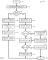
- FIG 6 is a high-level logic flow diagram of an illustrative memory integrity performance enhancement method 600, in accordance with at least one embodiment described herein.
- the method 600 commences at 602.
- the controller circuitry 110 receives a memory access request from the processor circuitry 150.
- the memory access request may be generated by one or more applications executed by the processor circuitry 150.
- the controller circuitry 110 determines whether the received memory access request includes a read request. Responsive to a determination by the controller circuitry 110 that the received memory access request IS NOT a read request, the method 600 continues at 608 Responsive to a determination by the controller circuitry 110 that the received memory access request IS a read request, the method 600 continues at 616.
- the controller circuitry 110 encrypts the received data line 132 and generates MAC data 136 for the encrypted data line 132.
- the controller circuitry 110 generates error correction code (ECC) data 138 for the encrypted data line 132.
- ECC data 138 includes error detection data (e.g., 64 bit error detection data) and error correction data (e.g., 32 bit error correction data).
- the controller circuitry 110 writes the encrypted data line 132, and Tier I metadata 134 including the MAC data 136 and the first portion of the ECC data 138 1 to the Tier I memory circuitry 130.
- the first portion of the ECC data 138 1 may include error detection data and, optionally, partial error correction data.
- the controller circuitry 110 writes Tier II metadata 142 including all or a portion of the second portion of the ECC data 138 2 to the Tier II memory circuitry 140.
- the second portion of the ECC data 138 2 may include some or all of the error correction data.
- the controller circuitry 110 communicates the read request to the memory circuitry 120.
- the read request retrieves the encrypted data line 132 and the Tier I metadata 134 (including the MAC data 136 and the first portion of the ECC data 138 1 along with any other data such as multi-level tag and state data) from the Tier I memory circuitry 130.
- the controller circuitry 110 determines whether errors exist in the retrieved, encrypted data line 132.
- the method 600 continues at 622. If the controller circuitry 110 fails to detect errors in the encrypted data line, the method 600 continues at 626.
- the controller circuitry 110 fetches the Tier II metadata 142, including the second portion of the ECC data 138 2 (including the remaining portion of the error correction data) from the Tier II memory circuitry 140.
- the controller circuitry 110 corrects the encrypted data line 132 using the error correction data included in the first portion of the ECC code 138 1 and/or the second portion of the ECC code 138 2 .
- the controller circuitry 110 simultaneously or sequentially decrypts the encrypted data line 132 and, using the MAC data 136 included in the Tier I metadata 134 and retrieved from the Tier I memory circuitry 130, verifies the data line 132.
- the controller circuitry 110 determines whether the verification of the data line 132 has failed or succeeded. Responsive to a successful verification of the data line 132 by the controller circuitry 110, the method 600 continues at 632. Responsive to an unsuccessful verification of the data line 132 by the controller circuitry 110, the method 600 continues at 630.
- the controller circuitry 110 signals an exception and may return a null value to the processor circuitry. The method 600 then concludes at 634.
- the controller circuitry 110 communicates the decrypted data line 132 to the processor circuitry 150.
- the method 600 then concludes at 634.
- FIG 6 illustrates various operations according to one or more embodiments, it is to be understood that not all of the operations depicted in FIG 6 are necessary for other embodiments. Indeed, it is fully contemplated herein that in other embodiments of the present disclosure, the operations depicted in FIG 6 , and/or other operations described herein, may be combined in a manner not specifically shown in any of the drawings, but still fully consistent with the present disclosure. Thus, claims directed to features and/or operations that are not exactly shown in one drawing are deemed within the scope and content of the present disclosure.
- a list of items joined by the term “and/or” can mean any combination of the listed items.
- the phrase “A, B and/or C” can mean A; B; C; A and B; A and C; B and C; or A, B and C.
- a list of items joined by the term "at least one of' can mean any combination of the listed terms.
- the phrases "at least one of A, B or C” can mean A; B; C; A and B; A and C; B and C; or A, B and C.
- system or “module” may refer to, for example, software, firmware and/or circuitry configured to perform any of the aforementioned operations.
- Software may be embodied as a software package, code, instructions, instruction sets and/or data recorded on non-transitory computer readable storage mediums.
- Firmware may be embodied as code, instructions or instruction sets and/or data that are hard-coded (e.g., nonvolatile) in memory devices.
- Circuitry may comprise, for example, singly or in any combination, hardwired circuitry, programmable circuitry such as computer processors comprising one or more individual instruction processing cores, state machine circuitry, and/or firmware that stores instructions executed by programmable circuitry or future computing paradigms including, for example, massive parallelism, analog or quantum computing, hardware embodiments of accelerators such as neural net processors and non-silicon implementations of the above.
- the circuitry may, collectively or individually, be embodied as circuitry that forms part of a larger system, for example, an integrated circuit (IC), system on-chip (SoC), desktop computers, laptop computers, tablet computers, servers, smartphones, etc.
- IC integrated circuit
- SoC system on-chip
- any of the operations described herein may be implemented in a system that includes one or more mediums (e.g., non-transitory storage mediums) having stored therein, individually or in combination, instructions that when executed by one or more processors perform the methods.
- the processor may include, for example, a server CPU, a mobile device CPU, and/or other programmable circuitry. Also, it is intended that operations described herein may be distributed across a plurality of physical devices, such as processing structures at more than one different physical location.
- the storage medium may include any type of tangible medium, for example, any type of disk including hard disks, floppy disks, optical disks, compact disk read-only memories (CD-ROMs), compact disk rewritables (CD-RWs), and magneto-optical disks, semiconductor devices such as read-only memories (ROMs), random access memories (RAMs) such as dynamic and static RAMs, erasable programmable read-only memories (EPROMs), electrically erasable programmable read-only memories (EEPROMs), flash memories, Solid State Disks (SSDs), embedded multimedia cards (eMMCs), secure digital input/output (SDIO) cards, magnetic or optical cards, or any type of media suitable for storing electronic instructions.
- ROMs read-only memories
- RAMs random access memories
- EPROMs erasable programmable read-only memories
- EEPROMs electrically erasable programmable read-only memories
- flash memories Solid State Disks (SSDs), embedded multimedia cards (eMMC
- a write request causes controller circuitry to write an encrypted data line and Tier I metadata including MAC data and a first portion of ECC data (error detection) to Tier I memory circuitry and a second portion of ECC data (error correction) to sequestered Tier II memory circuitry.
- a read request causes the controller circuitry to read the encrypted data line and the Tier I metadata from the Tier I memory circuitry.
- the controller circuitry uses the first portion of the ECC data included in the Tier I metadata the controller circuitry determines if an error exists in the encrypted data line. If no error is detected, the controller circuitry decrypts and verifies the data line using the MAC data. If an error in the data line is detected by the controller circuitry, the second portion of the ECC data is fetched from the Tier II memory circuitry and the error corrected.
- the following examples pertain to further embodiments.
- the following examples of the present disclosure may comprise subject material such as at least one device, a method, at least one machine-readable medium for storing instructions that when executed cause a machine to perform acts based on the method, means for performing acts based on the method and/or a system for providing scalable memory integrity and enhanced RAS using sequestered memory.
Landscapes
- Engineering & Computer Science (AREA)
- Theoretical Computer Science (AREA)
- Computer Security & Cryptography (AREA)
- General Engineering & Computer Science (AREA)
- General Physics & Mathematics (AREA)
- Physics & Mathematics (AREA)
- Computer Hardware Design (AREA)
- Software Systems (AREA)
- Signal Processing (AREA)
- Computer Networks & Wireless Communication (AREA)
- Quality & Reliability (AREA)
- Multimedia (AREA)
- Technology Law (AREA)
- Human Computer Interaction (AREA)
- Power Engineering (AREA)
- General Health & Medical Sciences (AREA)
- Bioethics (AREA)
- Health & Medical Sciences (AREA)
- Computing Systems (AREA)
- Techniques For Improving Reliability Of Storages (AREA)
- Detection And Correction Of Errors (AREA)
Abstract
Description
- The present disclosure relates to memory integrity, more specifically, this disclosure relates to error detection and correction systems having reduced overhead requirements.
- Cloud security providers (CSPs) use cryptographic isolation for the customer workloads running on their platform. Various cryptographic isolation methods have been implemented to meet these requirements for the cloud providers, such as Secure Memory Encryption (SME) and Secure Encrypted Virtualization (SEV). Memory integrity operates by associating a cryptographic message authentication code (MAC) with each data line in memory. The MAC is generated when data is written to memory and verified when the data is read from memory. If data was modified, either when resident in memory, the MAC will not match and result in the modification attack being detected (a security exception can then be signaled to notify software of the attack). Traditional integrity approaches can suffer from significant performance overheads as the MAC associated with each data line must be loaded on each access and verified/updated depending on the type of memory access. This additional access results in storage, performance, and bandwidth overheads.
- Features and advantages of various embodiments of the claimed subject matter will become apparent as the following Detailed Description proceeds, and upon reference to the Drawings, wherein like numerals designate like parts, and in which:
-
FIG 1 is a block diagram of an illustrative system that includes controller circuitry and memory circuitry that includes: Tier I memory circuitry to store data lines and associated Tier I metadata; and Tier II memory circuitry to store Tier II metadata associated with respective ones of the data lines, in accordance with at least one embodiment described herein; -
FIG 2A is an illustrative metadata configuration using a 10x4 DDR5 memory module, in accordance with at least one embodiment described herein; -
FIG 2B is another illustrative metadata configuration using a 9x4 DDR5 memory module, in accordance with at least one embodiment described herein; -
FIG 2C is yet another illustrative metadata configuration using a 5x8 DDR5 memory module, in accordance with at least one embodiment described herein; -
FIG 3 is a table providing a comparison of various metadata configurations, in accordance with at least one embodiment described herein; -
FIG 4 is a flow diagram of an illustrative method that depicts a read operation using the first portion of the ECC data stored in Tier I memory circuitry and read with the data line and the first portion of the ECC data stored in sequestered Tier II memory circuitry and read only upon detection of an error by the controller circuitry, in accordance with at least one embodiment described herein; -
FIG 5 and the following discussion provide a brief, general description of the components forming an illustrative processor-based device capable of implementing a scalable memory integrity and enhanced RAS system using sequestered memory such as depicted and described in detail inFIGs 1-4 (above), in accordance with at least one embodiment described herein; and -
FIG 6 is a high-level logic flow diagram of an illustrative memory integrity performance enhancement method, in accordance with at least one embodiment described herein. - Although the following Detailed Description will proceed with reference being made to illustrative embodiments, many alternatives, modifications and variations thereof will be apparent to those skilled in the art.
- The systems and methods disclosed herein provide a memory integrity architecture that features full error correction capabilities and high-strength memory integrity without introducing the performance overheads of traditional memory integrity approaches. The systems and methods disclosed herein use extended Reed-Solomon codes to provide error correction code (ECC) that includes error detection data and error correction data. The use of Reed-Solomon codes advantageously permits splitting the ECC into two tiers (hereinafter, "Tier I" and "Tier II"). Tier I data, including at least the error detection data and message authentication code (MAC) data, is stored in memory circuitry at the same location as the associated data line, such that at least the error detection data and MAC data are read during each read operation on the data line. The Tier I data may, at times, also include other data such as security-related metadata, and some or all of the error correction data. Tier II data includes error correction data and is stored in a separate or sequestered location in the memory circuitry. The Tier II error correction data is accessed when the memory controller circuitry detects an error in the data line. Thus, Tier I stores performance sensitive metadata (e.g., the error detection and correction tier of ECC, MAC) and Tier II uses sequestered memory to store the metadata associated with a data line that is off the performance critical path (e.g., the error correction tier of ECC). System performance is enhanced by obviating the need to read the MAC data and both the error detection data and error correction data during each read operation - instead, the MAC data and the error detection data are read during each read operation and only when a data error occurs is the full error correction data read.
- A data storage system is provided. The system may include: memory circuitry; controller circuitry to, for each of a plurality of lines of data stored in memory circuitry: generate metadata that includes: data representative of a cryptographic message authentication code associated with the respective line of data; and data representative of an error code associated with the respective line of data, the error correction code including at least error detection data associated with the respective line of data and error correction data associated with the respective line of data; and apportion the metadata into a Tier I portion stored in a first location in the memory circuitry proximate the respective line of data in the memory circuitry and a Tier II portion stored in a second location in the memory circuitry remote from the respective line of data; wherein the Tier I portion includes at least the error detection data portion and the message authentication code portion associated with the respective line of data; and wherein the Tier II portion includes at least a portion of the error correction data portion associated with the respective line of data.
- A data storage method is provided. The method may include: generating, by controller circuitry, metadata for each respective one of a plurality of lines of data stored in memory circuitry the metadata including: data representative of a cryptographic message authentication code (MAC) associated with the respective line of data; and data representative of an error correction code (ECC) associated with the respective line of data, the error correction code including at least error detection data associated with the respective line of data and error correction data associated with the respective line of data; and apportioning, by the controller circuitry, the metadata into a Tier I portion stored in a first memory location in the memory circuitry proximate the respective line of data and a Tier II portion stored in a second location in the memory circuitry remote from the respective line of data; wherein the Tier I portion includes at least the error detection data portion and the message authentication code portion of the metadata associated with the respective line of data; and wherein the Tier II portion includes at least a portion of the error correction data portion of the metadata associated with the respective line of data.
- A non-transitory storage device that includes instructions is provided. The instructions, when executed by controller circuitry, cause the controller circuitry to: generate metadata for each respective one of a plurality of lines of data stored in memory circuitry the metadata including: data representative of a cryptographic message authentication code (MAC) associated with the respective line of data; and data representative of an error correction code (ECC) associated with the respective line of data, the error correction code including at least error detection data associated with the respective line of data and error correction data associated with the respective line of data; and apportion the metadata into a Tier I portion stored in a first memory location in the memory circuitry proximate the respective line of data and a Tier II portion stored in a second location in the memory circuitry remote from the respective line of data; wherein the Tier I portion includes at least the error detection data portion and the message authentication code portion of the metadata associated with the respective line of data; and wherein the Tier II portion includes at least a portion of the error correction data portion of the metadata associated with the respective line of data.
- A data storage system is provided. The system may include: means for generating metadata for each respective one of a plurality of lines of data stored in memory circuitry the metadata including: data representative of a cryptographic message authentication code (MAC) associated with the respective line of data; and data representative of an error correction code (ECC) associated with the respective line of data, the error correction code including at least error detection data associated with the respective line of data and error correction data associated with the respective line of data; and means for apportioning the metadata into a Tier I portion stored in a first memory location in the memory circuitry proximate the respective line of data and a Tier II portion stored in a second location in the memory circuitry remote from the respective line of data; wherein the Tier I portion includes at least the error detection data portion and the message authentication code portion of the metadata associated with the respective line of data; and wherein the Tier II portion includes at least a portion of the error correction data portion of the metadata associated with the respective line of data.
- In the following description, certain specific details are set forth in order to provide a thorough understanding of various disclosed embodiments. However, one skilled in the relevant art will recognize that embodiments may be practiced without one or more of these specific details, or with other methods, components, materials, etc. In other instances, well-known structures associated with data storage and retrieval have not been shown or described in detail to avoid unnecessarily obscuring descriptions of the embodiments. Although the following disclosure is directed to specific embodiments utilizing electromagnetic memory such as random access memory (RAM); dual data rate RAM (DDR-RAM); static RAM (SRAM); and dynamic RAM (DRAM), those of ordinary skill in the computer arts will readily appreciate the applicability of the systems and methods disclosed herein to other data storage structures such as: magneto-resistive RAM (MRAM); spin transfer torque MRAM (STT-MRAM); resistive RAM (ReRAM); quantum storage devices; molecular storage devices; and similar.
- Unless the context requires otherwise, throughout the specification and claims which follow, the word "comprise" and variations thereof, such as, "comprises" and "comprising" are to be construed in an open, inclusive sense that is as "including, but not limited to."
- Reference throughout this specification to "one embodiment" or "an embodiment" means that a particular feature, structure or characteristic described in connection with the embodiment is included in at least one embodiment. Thus, the appearances of the phrases "in one embodiment" or "in an embodiment" in various places throughout this specification are not necessarily all referring to the same embodiment.
- The use of ordinals such as first, second and third does not necessarily imply a ranked sense of order, but rather may only distinguish between multiple instances of an act or structure.
- The headings and Abstract of the Disclosure provided herein are for convenience only and do not interpret the scope or meaning of the embodiments.
-
FIG 1 is a block diagram of an illustrative system 100 that includescontroller circuitry 110 andmemory circuitry 120 that includes: Tier Imemory circuitry 130 to storedata lines 132A-132n and associated Tier Imetadata 134A-134n; and Tier IImemory circuitry 140 to store Tier IImetadata 142A-142n associated with respective ones of thedata lines 132A-132n, in accordance with at least one embodiment described herein. As depicted inFIG 1 , the system 100 also includesprocessor circuitry 150 to execute one or more applications that perform memory operations such as memory read and memory write operations. - As depicted in
FIG 1 , the Tier Imetadata 134A-134n includes message authentication code (MAC)data 136A-136n, each associated with a respective one of thedata lines 132A-132n. The Tier Imetadata 134A-134n also includes at least a first portion of the error correction code (ECC) 138A1-138n1, each associated with a respective one of thedata lines 132A-132n. In some embodiments, the first portion of theECC 138A1-138n1 includes the error detection data portion of therespective ECC 138A-138n. In other embodiments, the first portion of theECC 138A1-138n1 includes the error detection data portion of therespective ECC 138A-138n and at least a portion of the error correction data portion of therespective ECC 138A-138n. Also as depicted inFIG 1 , the Tier IImetadata 142A-142n includes a second portion of the error correction code (ECC) 138A2-138n2, each associated with a corresponding one of thedata lines 132A-132n. - In embodiments, in response to execution of an instruction by the
processor circuitry 150 that includes a memory write operation, thecontroller circuitry 110 may encrypt thedata line 132A and generate message authentication code (MAC)data 136A that is associated with thedata line 132A. Thecontroller circuitry 110 may also generate an error correction code (ECC) 138A, such as a Reed-Solomon ECC, that includes error detection data and error correction data, both associated withdata line 132A. Thecontroller circuitry 110 stores thedata line 132A and the Tier Imetadata 134A, including at least theMAC data 136A and the first portion of theECC data 138A1 in the Tier Imemory circuitry 130. Thecontroller circuitry 110 stores the Tier IImetadata 142A, including the second portion of theECC data 138A2 in a sequestered Tier IImemory circuitry 140 that is remote from the Tier Imemory circuitry 130. - In embodiments, in response to execution of an instruction by the
processor circuitry 150 that includes a memory read operation, thecontroller circuitry 110 may retrieve thedata line 132A and the Tier Imetadata 134A, including theMAC data 136A and the first portion of theECC data 138A1, associated with thedata line 132A. Thecontroller circuitry 110 uses the error detection data included in the first portion of theECC data 138A1 to detect if errors exist in the retrieveddata 132A. If no errors are detected, thecontroller circuitry 110 decrypts and verifies the retrieveddata 132A using theMAC data 136A included in the Tier Imetadata 134A. Once verified by thecontroller circuitry 110, the verifieddata line 132A is then passed to theprocessor circuitry 150. If the retrieveddata 132A cannot be verified by thecontroller circuitry 110 using theMAC data 136A, thecontroller circuitry 110 returns null data and theprocessor circuitry 150 throws an exception. If thecontroller circuitry 110 detects an error in the retrieveddata line 132A, thecontroller circuitry 110 retrieves, from the Tier IImemory circuitry 140, the Tier IImetadata 142A. Thecontroller circuitry 110 uses the error correction data included in the second portion of the ECC data 138A2 to correct thedata line 132A prior to decrypting and verifying the retrieveddata 132A using theMAC data 136A included in the Tier I metadata 134A. - In embodiments, each of the data lines 132A-132n may include one or more lines in cache memory circuitry operably coupled to the
processor circuitry 150. For example, each of the data lines 132A-132n may include one or more level 1 (LI) cache lines; one or more level 2 (L2) cache lines; one or more last level cache (LLC) lines; or combinations thereof. Each of the data lines 132A-132n may include any number of bytes. In embodiments, each of the data lines 132A-132n may have the same or different number of bytes. For example, each ofdata lines 132A-132n may include: 32 bytes; 64 bytes; 128 bytes; or 256 bytes. - The Tier I metadata 134A-134n includes the
MAC data 136A-136n and the first portion of theECC data 138A1-138n1. In addition, in some embodiments, the Tier I metadata 134A-134n may include other data such as security data that includes but is not limited to: tag and state data, directory/poison data, and similar security related data. In some embodiments, the Tier I metadata 134A-134n may include only the first portion of theECC data 138A1-138n1. In other embodiments, the Tier I metadata 134A-134n may include the first portion of theECC data 138A1-138n1 and at least some of the bits included in the second portion of theECC data 138A2-138n2. In yet other embodiments, the Tier I metadata 134A-134n may include the first portion of theECC data 138A1-138n1 and the second portion of theECC data 138A2-138n2. The Tier I metadata 134A-134n may include any number of bits. For example, the Tier I metadata 134A-134n may include: 64 bits; 96 bits; 128 bits; or 256 bits. TheMAC data 136A-136n included in the Tier I metadata 134A-134n may include any number of bits. For example, theMAC data 136A-136n may include: 30 bits or less; 40 bits or less; 50 bits or less; or 60 bits or less. The first portion of theECC data 138A1-138n1 includes error detection data. In some embodiments, the first portion of theECC data 138A1-138n1 includes error detection data and at least a portion of the error correction data. The first portion of theECC data 138A1-138n1 may include any number of bits. For example, the first portion of theECC data 138A1-138n1 may include: 32 bits, 64 bits, 96 bits, or 128 bits. - In other embodiments, the Tier I metadata 134A-134n may include the first portion of the
ECC data 138A1-138n1 and at least some of the bits included in the second portion of theECC data 138A2-138n2. In such embodiments, the Tier I metadata 134A-134n may include any number of bits from the second portion of theECC data 138A2-138n2. For example, the Tier I metadata 134A-134n may include: 8 bits, 16 bits, or 32 bits of the second portion of theECC data 138A2-138n2. - In yet other embodiments, the Tier I metadata 134A-134n may include the first portion of the
ECC data 138A1-138n1 and the second portion of theECC data 138A2-138n2. In such embodiments, the Tier I metadata 134A-134n may include a total of: 64 bits, 96 bits, or 128 bits of ECC data included in the first portion of theECC data 138A1-138n1 and the second portion of theECC data 138A2-138n2. - The
Tier II metadata 142A-142n includes all or a portion of the second portion of theECC data 138A2-138n2. In embodiments, the second portion of theECC data 138A2-138n2 may include error correction data that includes any number of bits. For example, theTier II metadata 142A-142n may include: 8 bits, 16 bits, 32 bits, 64 bits, 96 bits, or 128 bits of error correction data included in the second portion of theECC data 138A2-138n2. - The
controller circuitry 110 includes any number and/or combination of currently available and/or future developed electronic components, optical components, semiconductor device, and/or logic elements capable of performing memory access, error detection, error correction, and verification operations on data communicated to or from thememory circuitry 130. In at least some embodiments, thecontroller circuitry 110 may include memory controller circuitry. In at least some embodiments, theprocessor circuitry 150 may provide all or a portion of thecontroller circuitry 110. - The
memory circuitry 120 includes any number and/or combination of currently available and/or future developed electronic components, optical components, semiconductor device, and/or logic elements capable of storing information and/or data. Thememory circuitry 120 may include volatile memory, non-volatile memory, or any combination thereof. Thememory circuitry 120 may be communicatively coupled toprocessor circuitry 150 that includes one or more processor core circuits, each processor core circuit capable of contemporaneous execution of one or more threads. In embodiments, thememory circuitry 120 may include cache memory circuitry communicatively coupled to the processor circuitry. In embodiments, thememory circuitry 120 may include level 1 (LI) cache memory circuitry, level 2 (L2) cache memory circuitry, last level cache (LLC) circuitry, or any combination thereof. In other embodiments, all or a portion of thecache memory circuitry 120 may include cache circuitry shared between a plurality of processor core circuits included in theprocessor circuitry 150. - The
processor circuitry 150 may include a general-purpose processor, such as a Core® i3, i5, i7, 2 Duo and Quad, Xeon®, Itanium®, Atom®, or Quark® microprocessor, available from Intel® (Intel Corporation, SANTA CLARA, CA), Alternatively, theprocessor circuitry 150 may include one or more processors from another manufacturer or supplier, such as Advanced Micro Devices (AMD®, Inc.), ARM Holdings® Ltd, MIPS®, etc. Theprocessor circuitry 150 may include a special-purpose processor, such as, for example, a network or communication processor, compression engine, graphics processor, co-processor, embedded processor, or the like. Theprocessor circuitry 150 may be implemented as a single semiconductor package or as a combination of stacked or otherwise interconnected semiconductor packages and/or dies. Theprocessor circuitry 150 may be a part of and/or may be implemented on one or more substrates using any of a number of process technologies, such as, for example, BiCMOS, CMOS, or NMOS. -
FIG 2A is anillustrative metadata configuration 200A using a 10x4 DDR5 memory module, in accordance with at least one embodiment described herein.FIG 2B is anotherillustrative metadata configuration 200B using a 9x4 DDR5 memory module, in accordance with at least one embodiment described herein.FIG 2C is yet another illustrative metadata configuration 200C using a 5x8 DDR5 memory module, in accordance with at least one embodiment described herein. Those of skill in the relevant arts will readily appreciate thatFIGS 2A, 2B , and2C represent illustrative embodiments, and the general principles behind the systems and methods disclosed herein may be readily applied to other memory module configurations with similar impact on system performance as described herein. - As depicted in
FIG 2A , the 10x4DDR5 memory module 200A includes 10 storage devices, with 8storage devices 202A-202H dedicated to the storage of data and 2storage devices 204A and 204B dedicated to the storage ofECC data 138. Each data storage device 202 and each ECC storage device 204 provides 4 bytes of data in each cycle with a 64 byte cache line requiring a total of 16 cycles to be read out of the 10x4DDR5 memory module 200A. - Turning next to
FIG 2B , the 9x4DDR5 memory module 200B includes 9 storage devices, with 8storage devices 202A-202H dedicated to the storage of data and 1storage device 204A dedicated to the storage ofECC data 138. Each data storage device 202 and each ECC storage device 204 provides 4 bytes of data in each cycle with a 64 byte cache line again requiring a total of 16 cycles to be read out of the 9x4DDR5 memory module 200B. - Turning next to
FIG 2C , the 5x8 DDR5 memory module 200C includes 9 storage devices, with 4storage devices 206A-206D dedicated to the storage of data and 1storage device 208A dedicated to the storage ofECC data 138. Each data storage device 206 and each ECC storage device 208 provides 8 bytes of data in each cycle with a 128 byte cache line requiring a total of 16 cycles to be read out of the 5x8 DDR5 memory module 200C. -
FIG 3 is a table 300 providing a comparison ofvarious metadata configurations FIG 3 , abase metadata configuration 310 in which all of the metadata, including a 64 bits of error detection + correction data, 32 bits of error correction data, 28 bits of MAC data and 4 bits of security (or other) data fit within the 128 bits allowable in the Tier Imemory circuitry 130. Inconfiguration 310, the MAC data is limited to 28 bits and the security data is limited to 4 bits to fit within the 128 bit constraint of the TierI memory circuitry 130. -
Configuration 320 provides a first metadata configuration in which theECC data 138 is split into a first portion ofECC data 1381 stored or otherwise retained in the Tier Imemory circuitry 130 and a second portion ofECC data 1382 stored or otherwise retained in the Tier IImemory circuitry 140. As depicted inconfiguration 320, the TierI memory circuitry 130 stores or otherwise retains the first portion of the ECC data 1381 (64 bits of error detection + partial error correction data), and a portion of the second portion of the ECC data 1382 (16 bits of partial error correction data). The sequestered Tier IImemory circuitry 140 stores or otherwise retains the remaining portion of the second portion of the ECC data 1382 (16 bits of remaining error correction data). The Tier Imemory circuitry 130 is read on every memory read operation, thereby permitting error detection capabilities. Thecontroller circuitry 110 accesses the second portion of the ECC data 1382 (16 bits of remaining error correction data) in sequestered Tier IImemory circuitry 140 only upon detecting an error. Tier I memory circuitry allocated to the storage ofMAC data 136 has increased to 34 bits, providing an additional 6 bits of MAC data storage.Metadata configuration 320 beneficially provides increased capability for storage of other data - as depicted inconfiguration 320, up to 14 bits of other data. An example of such data includes but is not limited to tag bits used to support multi-level memory circuitry (e.g., three-dimensional cross point memory circuitry "3DXP" memory circuitry as provided by Intel® Corp., SANTA CLARA, CA). -
Configuration 330 provides a second metadata configuration in which Tier Imemory circuitry 130 contains the first portion of ECC data 1381 (error detection + partial correction data) and Tier IImemory circuitry 140 contains the second portion of ECC data 1382 (remaining error correction data). As depicted inconfiguration 330, the TierI memory circuitry 130 stores the first portion of the ECC data 1381 (64 bits of error detection + partial correction data), 50 bits of MAC data, and 14 bits of other data (multi-level memory tag and state, Directory/Poison and other security related metadata). The sequestered Tier IImemory circuitry 140 stores the second portion of the ECC data 1382 (32 bits of remaining error correction). The Tier Imemory circuitry 130, including the first portion of theECC data 1381, containing the error detection data, is read on every memory read operation, thereby permitting error detection capabilities. Thecontroller circuitry 110 accesses the second portion of the ECC data 1382 (32 bits of remaining error correction data) in sequestered Tier IImemory circuitry 140 only upon detecting an error. Tier I memory circuitry allocated to the storage ofMAC data 136 has increased to 50 bits, providing an additional 22 bits of MAC data storage over thebase configuration 310. Similar tometadata configuration 320,metadata configuration 330 beneficially provides increased capability for storage of other data, up to 14 bits of other data. -
Configuration 340 provides a third metadata configuration in which Tier Imemory circuitry 130 contains the first portion of ECC data 1381 (error detection + partial correction data) and Tier IImemory circuitry 140 contains the second portion of ECC data 1382 (remaining error correction data). As depicted inconfiguration 340, the TierI memory circuitry 130 stores the first portion of the ECC data 1381 (64 bits of error detection + partial correction data), 55 bits of MAC data, and 9 bits of other data (multi-level memory tag and state and other security related metadata). The sequestered Tier IImemory circuitry 140 stores the second portion of the ECC data 1382 (64 bits of remaining error correction). The Tier Imemory circuitry 130, including the first portion of theECC data 1381, containing the error detection data, is read on every memory read operation, thereby permitting error detection capabilities. Thecontroller circuitry 110 accesses the second portion of the ECC data 1382 (64 bits of remaining error correction data) in sequestered Tier IImemory circuitry 140 only upon detecting an error. Tier I memory circuitry allocated to the storage ofMAC data 136 has increased to 50 bits, providing enhanced security by providing an additional 27 bits of memory circuitry to storeMAC data 136 over thebase metadata configuration 310. -
FIG 4 is a flow diagram of anillustrative method 400 that depicts a read operation using the first portion of theECC data 1381 stored in Tier Imemory circuitry 130 and read with the data line 312 and the first portion of theECC data 1382 stored in sequestered Tier IImemory circuitry 140 and read only upon detection of an error by thecontroller circuitry 110, in accordance with at least one embodiment described herein. As depicted inFIG 4 , thecontroller circuitry 110 may includemulti-key circuitry 412, encryption/decryption circuitry 414,verification circuitry 416, and metadata fetch andcaching circuitry 418. - Upon receipt of a read
request operation 410 generated by an application executed by theprocessor circuitry 150, thecontroller circuitry 110 forwards the read request tomemory controller circuitry 430. Theencrypted data line 132 and the associated Tier I metadata 132, including theMAC data 136, first portion of theECC data 1381, and other data such as multi-level memory tag and state data, is returned 450 to thecontroller circuitry 110. Thecontroller circuitry 110 first determines whether errors exist in theencrypted data line 132 using the error detection data included in the first portion of theECC data 1381. Responsive to thecontroller circuitry 110 not detecting errors in theencrypted data line 132, thedata line 132 may be simultaneously or sequentially decrypted by the encryption/decryption circuitry 414 and verified using theMAC data 136 by theverification circuitry 416. If thecontroller circuitry 110 detects errors in theencrypted data line 132, thecontroller circuitry 110fetches 470 the second portion of theECC data 1382 from the sequestered Tier IImemory circuitry 140 and, using the error correction data retrieved from the Tier IImemory circuitry 140 and/or the Tier I memory circuitry, repairs theencrypted data line 132. Responsive to a successful verification of thedata line 132 by theverification circuitry 416, the decrypteddata line 132 is returned 490 to theprocessor circuitry 150. -
FIG 5 and the following discussion provide a brief, general description of the components forming an illustrative processor-baseddevice 500 capable of implementing a scalable memory integrity and enhanced RAS system using sequestered memory such as depicted and described in detail inFIGs 1-4 (above), in accordance with at least one embodiment described herein. The processor-baseddevice 500 includesprocessor circuitry 150. Theprocessor circuitry 150 executes one or more applications. During execution, the applications may cause theprocessor circuitry 150 to perform one or more memory operations, such as a memory write operation or a memory read operation. As depicted inFIG 5 , in some embodiments, theprocessor circuitry 150 may includememory circuitry 120, for example as processor cache circuitry. In embodiments, theprocessor memory circuitry 120 may include some or all of the TierI memory circuitry 130. As depicted inFIG 5 , in embodiments,system memory circuitry 510 may include some or all of the sequestered Tier IImemory circuitry 140. Although not depicted inFIG 5 , in other embodiments, theprocessor memory circuitry 120 may provide all or a portion of the Tier IImemory circuitry 140. For example,processor memory circuitry 120, such as L1 cache memory circuitry may be used to provide all or a portion of the TierI memory circuitry 130 and LLC cache memory circuitry may be used to provide all or a portion of the Tier IImemory circuitry 140. Those skilled in the relevant art will appreciate that the illustrated embodiments as well as other embodiments can be practiced with other circuit-based device configurations, including portable electronic or handheld electronic devices, for instance smartphones, portable computers, wearable computers, microprocessor-based or programmable consumer electronics, personal computers ("PCs"), network PCs, minicomputers, mainframe computers, and the like. The embodiments can be practiced in distributed computing environments where tasks or modules are performed by remote processing devices, which are linked through a communications network. In a distributed computing environment, program modules may be located in both local and remote memory storage devices. - The
processor circuitry 150 and/or thecontroller circuitry 110 may include any number of circuits, some or all of which may include programmable and/or configurable combinations of electronic components, semiconductor devices, and/or logic elements that are disposed partially or wholly in a PC, server, or other computing system capable of executing machine-readable instructions. The processor-baseddevice 500 may includeprocessor circuitry 150, and may, at times, include a bus or similar communications link 516 that communicatively couples and facilitates the exchange of information and/or data between various system components including asystem memory 510 and theprocessor circuitry 150. The processor-baseddevice 500 may be referred to in the singular herein, but this is not intended to limit the embodiments to a single device and/or system, since in certain embodiments, there will be more than one processor-baseddevice 500 that incorporates, includes, or contains any number of communicably coupled, collocated, or remote networked circuits or devices. - The
processor circuitry 150 may include any number, type, or combination of devices. At times, theprocessor circuitry 150 may be implemented in whole or in part in the form of semiconductor devices such as diodes, transistors, inductors, capacitors, and resistors. Such an implementation may include, but is not limited to any current or future developed single- or multi-core processor or microprocessor, such as: on or more systems on a chip (SOCs); central processing units (CPUs); digital signal processors (DSPs); graphics processing units (GPUs); application-specific integrated circuits (ASICs), field programmable gate arrays (FPGAs), and the like. Unless described otherwise, the construction and operation of the various blocks shown inFIG. 5 are of conventional design. As a result, such blocks need not be described in further detail herein, as they will be understood by those skilled in the relevant art. The communications link 316 that interconnects at least some of the components of the processor-baseddevice 500 may employ any known serial or parallel bus structures or architectures. - The
system memory 510 may include read-only memory ("ROM")circuitry 518 and random access memory ("RAM")circuitry 520. A portion of theROM circuitry 518 may be used to store or otherwise retain a basic input/output system ("BIOS") 522. TheBIOS 522 provides basic functionality to the processor-baseddevice 500, for example by causing theprocessor circuitry 150 to load anoperating system 536, one or more machine-readable instruction sets 538, and/ordata 540 from theRAM circuitry 520. In embodiments, at least some of the one or more machine-readable instruction sets cause thecontroller circuitry 110 to selectively provide the memory integrity performance enhancement system as described herein.. - The processor-based
device 500 may include one or more communicably coupled, non-transitory,data storage devices 530. Although depicted inFIG 5 as disposed internal to the processor-baseddevice 500, in various embodiments, the one or moredata storage devices 530 may be disposed local to and/or remote from the processor-baseddevice 500. The one or moredata storage devices 530 may include any current or future developed storage appliances, networks, and/or devices. Non-limiting examples of suchdata storage devices 530 may include, but are not limited to, any current or future developed non-transitory storage appliances or devices, such as one or more magnetic storage devices, one or more optical storage devices, one or more solid-state electromagnetic storage devices, one or more electro-resistive storage devices, one or more molecular storage devices, one or more quantum storage devices, or various combinations thereof. In some implementations, the one or moredata storage devices 530 may include one or more removable storage devices, such as one or more flash drives, flash memories, flash storage units, or similar appliances or devices capable of communicable coupling to and decoupling from the processor-baseddevice 500. - The one or
more storage devices 530 may include interfaces or controllers (not shown inFIG 5 ) communicatively coupling therespective storage device 530 or system to the communications link 316. The one ormore storage devices 530 may contain machine-readable instruction sets, data structures, program modules, data stores, databases, logical structures, and/or other data useful to theprocessor circuitry 150 and/or thecontroller circuitry 110. In some instances, one or moreexternal storage devices 530 may be communicably coupled to theprocessor circuitry 150, for example via communications link 310 or via one or more wired communications interfaces (e.g., Universal Serial Bus or USB); one or more wireless communications interfaces (e.g., Bluetooth®, Near Field Communication or NFC); one or more wired network interfaces (e.g., IEEE 802.3 or Ethernet); and/or one or more wireless network interfaces (e.g., IEEE 802.11 or WiFi®). - Machine-
readable instruction sets 538 anddata 540 may be stored in whole or in part in thesystem memory 510.Such instruction sets 538 may be transferred, in whole or in part, from one or more internal data storage devices and/or one or moreexternal storage devices 530. The instruction sets 538 may be loaded, stored, or otherwise retained insystem memory 510, in whole or in part, during execution by theprocessor circuitry 150. The machine-readable instruction sets 538 may include machine-readable and/or processor-readable code, instructions, or similar logic capable of providing the memory integrity performance enhancement functions and capabilities described herein. - For example, the one or more machine-
readable instruction sets 538 may cause thecontroller circuitry 110 to, in response to a write operation received from theprocessor circuitry 150, encrypt and generate message authentication code (MAC)data 136 associated with thedata line 132 to be written to thememory circuitry 120. The instruction sets 538 may further cause the controller circuitry to generate errorcorrection code data 138 associated with theencrypted data line 132. The instruction sets 538 may further cause thecontroller circuitry 110 to write Tier I metadata 134, including theMAC data 136 and a first portion of ECC data 1381 (error detection data + (optionally) partial error correction data) to the TierI memory circuitry 130. The instruction sets 538 may further cause thecontroller circuitry 110 to write Tier IImetadata 142, including a second portion of ECC data 1382 (full or partial error correction data) to the Tier IImemory circuitry 140. - The one or more machine-
readable instruction sets 538 may cause thecontroller circuitry 110 to, in response to a read operation received from theprocessor circuitry 150, to retrieve the Tier I metadata 134, including theMAC data 136 and a first portion of ECC data 1381 (error detection data + (optionally) partial error correction data) from the Tier Imemory circuitry 130. The instruction sets 538 may further cause thecontroller circuitry 110 to detect the presence of errors in theencrypted data line 132 using the error detection data included in the first portion ofECC data 1381. Responsive to detecting an error in theencrypted data line 132, theinstruction sets 538 may further cause thecontroller circuitry 110 to fetch the second portion ofECC data 1382 from the sequestered Tier IImemory circuitry 140 and correct the errors in theencrypted data line 132 using the error correction data included in the first portion ofECC data 1381 and the second portion ofECC data 1382. Responsive to detecting no errors in theencrypted data line 132 or after repairing the errors present in theencrypted data line 132, theinstruction sets 538 may cause thecontroller circuitry 110 to simultaneously or sequentially decrypt theencrypted data line 132 and verify the data included in thedata line 132 using theMAC data 136 included in the first portion ofECC data 1381. Responsive to a successful verification of thedata line 132, theinstruction sets 538 may cause thecontroller circuitry 110 to forward thedata line 132 to theprocessor circuitry 150. Responsive to an unsuccessful verification of thedata line 132, theinstruction sets 538 may cause thecontroller circuitry 110 to generate an exception and/or return a null value to theprocessor circuitry 150. - Processor-based device users may provide, enter, or otherwise supply commands (e.g., acknowledgements, selections, confirmations, and similar) as well as information and/or data (e.g., subject identification information, color parameters) to the processor-based
device 500 using one or more communicatively coupledphysical input devices 550 such as one or more text entry devices 551 (e.g., keyboard), one or more pointing devices 552 (e.g., mouse, trackball, touchscreen), and/or one or moreaudio input devices 553. Some or all of thephysical input devices 550 may include a wired or a wireless communicable coupling to the processor-baseddevice 500. - Processor-based device users may receive output from the processor-based
device 500 via one or morephysical output devices 554. In at least some implementations, the one or morephysical output devices 554 may include but are not limited to one or more: video output ordisplay devices 555;tactile output devices 556;audio output devices 557, or combinations thereof. Some or all of thephysical input devices 550 and some or all of thephysical output devices 554 may be communicatively coupled to the processor-baseddevice 500 via one or more wired or wireless interfaces. - For convenience, a
network interface 560, theprocessor circuitry 150, thecontroller circuitry 110, thesystem memory 510, thephysical input devices 550 and thephysical output devices 554 are illustrated as communicatively coupled to each other via the communications link 516, thereby providing connectivity between the above-described components. In alternative embodiments, the above-described components may be communicatively coupled in a different manner than illustrated inFIG 5 . For example, one or more of the above-described components may be directly coupled to other components, or may be coupled to each other, via one or more intermediary components (not shown). In some embodiments, all or a portion of the communications link 516 may be omitted and the components are coupled directly to each other using suitable wired or wireless connections. -
FIG 6 is a high-level logic flow diagram of an illustrative memory integrityperformance enhancement method 600, in accordance with at least one embodiment described herein. Themethod 600 commences at 602. - At 604, the
controller circuitry 110 receives a memory access request from theprocessor circuitry 150. In at least some embodiments, the memory access request may be generated by one or more applications executed by theprocessor circuitry 150. - At 606, the
controller circuitry 110 determines whether the received memory access request includes a read request. Responsive to a determination by thecontroller circuitry 110 that the received memory access request IS NOT a read request, themethod 600 continues at 608 Responsive to a determination by thecontroller circuitry 110 that the received memory access request IS a read request, themethod 600 continues at 616. - At 608, responsive to a determination by the
controller circuitry 110 that the received memory access request IS NOT a read request, thecontroller circuitry 110 encrypts the receiveddata line 132 and generatesMAC data 136 for theencrypted data line 132. - At 610, the
controller circuitry 110 generates error correction code (ECC)data 138 for theencrypted data line 132. In embodiments, theECC data 138 includes error detection data (e.g., 64 bit error detection data) and error correction data (e.g., 32 bit error correction data). - At 612, the
controller circuitry 110 writes theencrypted data line 132, and Tier I metadata 134 including theMAC data 136 and the first portion of theECC data 1381 to the TierI memory circuitry 130. In embodiments, the first portion of theECC data 1381 may include error detection data and, optionally, partial error correction data. - At 614, the
controller circuitry 110 writes Tier IImetadata 142 including all or a portion of the second portion of theECC data 1382 to the Tier IImemory circuitry 140. In embodiments, the second portion of theECC data 1382 may include some or all of the error correction data. Themethod 600 then concludes at 634. - At 616, responsive to a determination by the
controller circuitry 110 that the received memory access request IS a read request, thecontroller circuitry 110, communicates the read request to thememory circuitry 120. The read request retrieves theencrypted data line 132 and the Tier I metadata 134 (including theMAC data 136 and the first portion of theECC data 1381 along with any other data such as multi-level tag and state data) from the Tier Imemory circuitry 130. - At 618, using the error detection data included in the first portion of the
ECC data 1381, thecontroller circuitry 110 determines whether errors exist in the retrieved,encrypted data line 132. - At 620, if the
controller circuitry 110 detects errors in theencrypted data line 132, themethod 600 continues at 622. If thecontroller circuitry 110 fails to detect errors in the encrypted data line, themethod 600 continues at 626. - At 622, responsive to a determination by the
controller circuitry 110 that theencrypted data line 132 contains errors, thecontroller circuitry 110 fetches the Tier IImetadata 142, including the second portion of the ECC data 1382 (including the remaining portion of the error correction data) from the Tier IImemory circuitry 140. - At 624, the
controller circuitry 110 corrects theencrypted data line 132 using the error correction data included in the first portion of theECC code 1381 and/or the second portion of theECC code 1382. - At 626, the
controller circuitry 110 simultaneously or sequentially decrypts theencrypted data line 132 and, using theMAC data 136 included in the Tier I metadata 134 and retrieved from the Tier Imemory circuitry 130, verifies thedata line 132. - At 628, the
controller circuitry 110 determines whether the verification of thedata line 132 has failed or succeeded. Responsive to a successful verification of thedata line 132 by thecontroller circuitry 110, themethod 600 continues at 632. Responsive to an unsuccessful verification of thedata line 132 by thecontroller circuitry 110, themethod 600 continues at 630. - At 630, responsive to an unsuccessful verification of the
data line 132 at 628, thecontroller circuitry 110 signals an exception and may return a null value to the processor circuitry. Themethod 600 then concludes at 634. - At 632, responsive to a successful verification of the
data line 132 at 628, thecontroller circuitry 110 communicates the decrypteddata line 132 to theprocessor circuitry 150. Themethod 600 then concludes at 634. - While
FIG 6 illustrates various operations according to one or more embodiments, it is to be understood that not all of the operations depicted inFIG 6 are necessary for other embodiments. Indeed, it is fully contemplated herein that in other embodiments of the present disclosure, the operations depicted inFIG 6 , and/or other operations described herein, may be combined in a manner not specifically shown in any of the drawings, but still fully consistent with the present disclosure. Thus, claims directed to features and/or operations that are not exactly shown in one drawing are deemed within the scope and content of the present disclosure. - As used in this application and in the claims, a list of items joined by the term "and/or" can mean any combination of the listed items. For example, the phrase "A, B and/or C" can mean A; B; C; A and B; A and C; B and C; or A, B and C. As used in this application and in the claims, a list of items joined by the term "at least one of' can mean any combination of the listed terms. For example, the phrases "at least one of A, B or C" can mean A; B; C; A and B; A and C; B and C; or A, B and C.
- As used in any embodiment herein, the terms "system" or "module" may refer to, for example, software, firmware and/or circuitry configured to perform any of the aforementioned operations. Software may be embodied as a software package, code, instructions, instruction sets and/or data recorded on non-transitory computer readable storage mediums. Firmware may be embodied as code, instructions or instruction sets and/or data that are hard-coded (e.g., nonvolatile) in memory devices. "Circuitry", as used in any embodiment herein, may comprise, for example, singly or in any combination, hardwired circuitry, programmable circuitry such as computer processors comprising one or more individual instruction processing cores, state machine circuitry, and/or firmware that stores instructions executed by programmable circuitry or future computing paradigms including, for example, massive parallelism, analog or quantum computing, hardware embodiments of accelerators such as neural net processors and non-silicon implementations of the above. The circuitry may, collectively or individually, be embodied as circuitry that forms part of a larger system, for example, an integrated circuit (IC), system on-chip (SoC), desktop computers, laptop computers, tablet computers, servers, smartphones, etc.
- Any of the operations described herein may be implemented in a system that includes one or more mediums (e.g., non-transitory storage mediums) having stored therein, individually or in combination, instructions that when executed by one or more processors perform the methods. Here, the processor may include, for example, a server CPU, a mobile device CPU, and/or other programmable circuitry. Also, it is intended that operations described herein may be distributed across a plurality of physical devices, such as processing structures at more than one different physical location. The storage medium may include any type of tangible medium, for example, any type of disk including hard disks, floppy disks, optical disks, compact disk read-only memories (CD-ROMs), compact disk rewritables (CD-RWs), and magneto-optical disks, semiconductor devices such as read-only memories (ROMs), random access memories (RAMs) such as dynamic and static RAMs, erasable programmable read-only memories (EPROMs), electrically erasable programmable read-only memories (EEPROMs), flash memories, Solid State Disks (SSDs), embedded multimedia cards (eMMCs), secure digital input/output (SDIO) cards, magnetic or optical cards, or any type of media suitable for storing electronic instructions. Other embodiments may be implemented as software executed by a programmable control device.
- Thus, the present disclosure is directed to systems and methods for providing a scalable memory integrity and enhanced RAS using sequestered memory. A write request causes controller circuitry to write an encrypted data line and Tier I metadata including MAC data and a first portion of ECC data (error detection) to Tier I memory circuitry and a second portion of ECC data (error correction) to sequestered Tier II memory circuitry. A read request causes the controller circuitry to read the encrypted data line and the Tier I metadata from the Tier I memory circuitry. Using the first portion of the ECC data included in the Tier I metadata the controller circuitry determines if an error exists in the encrypted data line. If no error is detected, the controller circuitry decrypts and verifies the data line using the MAC data. If an error in the data line is detected by the controller circuitry, the second portion of the ECC data is fetched from the Tier II memory circuitry and the error corrected.
- The following examples pertain to further embodiments. The following examples of the present disclosure may comprise subject material such as at least one device, a method, at least one machine-readable medium for storing instructions that when executed cause a machine to perform acts based on the method, means for performing acts based on the method and/or a system for providing scalable memory integrity and enhanced RAS using sequestered memory.
- According to example 1 a data storage system. The system may include: memory circuitry; controller circuitry to, for each of a plurality of lines of data stored in memory circuitry: generate metadata that includes: data representative of a cryptographic message authentication code associated with the respective line of data; and data representative of an error code associated with the respective line of data, the error correction code including at least error detection data associated with the respective line of data and error correction data associated with the respective line of data; and apportion the metadata into a Tier I portion stored in a first location in the memory circuitry proximate the respective line of data in the memory circuitry and a Tier II portion stored in a second location in the memory circuitry remote from the respective line of data; wherein the Tier I portion includes at least the error detection data portion and the message authentication code portion associated with the respective line of data; and wherein the Tier II portion includes at least a portion of the error correction data portion associated with the respective line of data.
- Example 2 may include elements of example 1, and the controller circuitry may further: responsive to receipt of a read operation generated by an application executed by processor circuitry: retrieve the requested line of data and the Tier I portion of the metadata from the first location in the memory circuitry; determine whether an error exists in the requested line of data using the error detection data portion included in the Tier I portion of the metadata and associated with the requested line of data; and decrypt the requested line of data responsive to a determination that the requested line of data contains no errors.
- Example 3 may include elements of any of
claims - Example 4 may include elements of any of examples 1 through 3 and the controller circuitry may further: generate a security exception responsive to an unsuccessful verification of the requested line of data.
- Example 5 may include elements of any of examples 1 through 4 and the controller circuitry may further: retrieve the Tier II portion of the metadata from the second memory location responsive to a determination that the requested line of data contains an error; and correct the error in the requested line of data using the error correction data portion included in the Tier II portion of the metadata.
- Example 6 may include elements of any of examples 1 through 5 where at least a portion of the memory circuitry comprises cache memory circuitry.
- Example 7 may include elements of any of examples 1 through 6 where the first portion of memory circuitry to store the Tier I metadata comprises memory circuitry capable of providing up to 128 bits of storage.
- Example 8 may include elements of any of examples 1 through 7 where the second portion of memory circuitry to store the Tier II metadata comprises memory circuitry capable of providing up to 64 bits of storage.
- According to example 9, there is provided a data storage method. The method may include: generating, by controller circuitry, metadata for each respective one of a plurality of lines of data stored in memory circuitry the metadata including: data representative of a cryptographic message authentication code (MAC) associated with the respective line of data; and data representative of an error correction code (ECC) associated with the respective line of data, the error correction code including at least error detection data associated with the respective line of data and error correction data associated with the respective line of data; and apportioning, by the controller circuitry, the metadata into a Tier I portion stored in a first memory location in the memory circuitry proximate the respective line of data and a Tier II portion stored in a second location in the memory circuitry remote from the respective line of data; wherein the Tier I portion includes at least the error detection data portion and the message authentication code portion of the metadata associated with the respective line of data; and wherein the Tier II portion includes at least a portion of the error correction data portion of the metadata associated with the respective line of data.
- Example 10 may include elements of example 9, and the method may further include: responsive to receipt of a read operation generated by an application executed by processor circuitry: retrieving, by the controller circuitry, the requested line of data and the Tier I portion of the metadata from the first location in the memory circuitry; determining, by the controller circuitry, whether an error exists in the requested line of data using the error detection data portion included in the Tier I portion of the metadata and associated with the requested line of data; and decrypting, by the controller circuitry, the requested line of data responsive to a determination that the requested line of data contains no errors.
- Example 11 may include elements of any of examples 9 or 10 and the method may further include: verifying, by the controller circuitry, the requested line of data using the message authentication code portion included in the Tier I portion of the metadata, responsive to no error being present in the requested line of data; and, responsive to a successful verification of the requested line of data, transferring the requested line of data to the processor circuitry.
- Example 12 may include elements of any of examples 9 through 11 and the method may further include: generating, by the controller circuitry, a security exception responsive to an unsuccessful verification of the requested line of data.
- Example 13 may include elements of any of examples 9 through 12 and the method may further include: retrieving, by the controller circuitry, the Tier II portion of the metadata from the second memory location responsive to a determination that the requested line of data contains an error; and correcting, by the controller circuitry, the error in the requested line of data using the error correction data portion included in the Tier II portion of the metadata.
- According to example 14, there is provided a non-transitory storage device that includes instructions. The instructions, when executed by controller circuitry, cause the controller circuitry to: generate metadata for each respective one of a plurality of lines of data stored in memory circuitry the metadata including: data representative of a cryptographic message authentication code (MAC) associated with the respective line of data; and data representative of an error correction code (ECC) associated with the respective line of data, the error correction code including at least error detection data associated with the respective line of data and error correction data associated with the respective line of data; and apportion the metadata into a Tier I portion stored in a first memory location in the memory circuitry proximate the respective line of data and a Tier II portion stored in a second location in the memory circuitry remote from the respective line of data; wherein the Tier I portion includes at least the error detection data portion and the message authentication code portion of the metadata associated with the respective line of data; and wherein the Tier II portion includes at least a portion of the error correction data portion of the metadata associated with the respective line of data.
- Example 15 may include elements of example 14 where the instructions, when executed by the controller circuitry, cause the controller circuitry to further: responsive to receipt of a read operation generated by an application executed by processor circuitry: retrieve the requested line of data and the Tier I portion of the metadata from the first location in the memory circuitry; determine whether an error exists in the requested line of data using the error detection data portion included in the Tier I portion of the metadata and associated with the requested line of data; and decrypt the requested line of data responsive to a determination that the requested line of data contains no errors.
- Example 16 may include elements of any of examples 14 or 15 where the instructions, when executed by the controller circuitry, cause the controller circuitry to further: verify the requested line of data using the message authentication code portion included in the Tier I portion of the metadata, responsive to no error being present in the requested line of data; and, responsive to a successful verification of the requested line of data, transfer the requested line of data to the processor circuitry.
- Example 17 may include elements of any of examples 14 through 16 where the instructions, when executed by the controller circuitry, cause the controller circuitry to further: generate a security exception responsive to an unsuccessful verification of the requested line of data.
- Example 18 may include elements of any of examples 14 through 17 where the instructions, when executed by the controller circuitry, cause the controller circuitry to further: retrieve the Tier II portion of the metadata from the second memory location responsive to a determination that the requested line of data contains an error; and correct the error in the requested line of data using the error correction data portion included in the Tier II portion of the metadata.
- According to example 19, there is provided a data storage system. The system may include: means for generating metadata for each respective one of a plurality of lines of data stored in memory circuitry the metadata including: data representative of a cryptographic message authentication code (MAC) associated with the respective line of data; and data representative of an error correction code (ECC) associated with the respective line of data, the error correction code including at least error detection data associated with the respective line of data and error correction data associated with the respective line of data; and means for apportioning the metadata into a Tier I portion stored in a first memory location in the memory circuitry proximate the respective line of data and a Tier II portion stored in a second location in the memory circuitry remote from the respective line of data; wherein the Tier I portion includes at least the error detection data portion and the message authentication code portion of the metadata associated with the respective line of data; and wherein the Tier II portion includes at least a portion of the error correction data portion of the metadata associated with the respective line of data.
- Example 20 may include elements of example 19 and the system may further include: means for retrieving the requested line of data and the Tier I portion of the metadata from the first location in the memory circuitry responsive to receipt of a read operation generated by an application executed by processor circuitry; means for determining whether an error exists in the requested line of data using the error detection data portion included in the Tier I portion of the metadata and associated with the requested line of data; and means for decrypting the requested line of data responsive to a determination that the requested line of data contains no errors.
- Example 21 may include elements of any of examples 19 or 20 and the system may further include: means for verifying the requested line of data using the message authentication code portion included in the Tier I portion of the metadata, responsive to no error being present in the requested line of data; and means for transferring the requested line of data to the processor circuitry responsive to a successful verification of the requested line of data.
- Example 22 may include elements of any of examples 19 through 21 and the system may further include: means for generating a security exception responsive to an unsuccessful verification of the requested line of data.
- Example 23 may include elements of any of examples 19 through 22 and the system may further include: means for retrieving the Tier II portion of the metadata from the second memory location responsive to a determination that the requested line of data contains an error; and means for correcting the error in the requested line of data using the error correction data portion included in the Tier II portion of the metadata.
- According to example 24, there is provided a system for providing scalable memory integrity and enhanced RAS using sequestered memory, the system being arranged to perform the method of any of examples 9 through 13.
- According to example 25, there is provided a chipset arranged to perform the method of any of examples 9 through 13.
- According to example 26, there is provided at least one, non-transitory, machine readable medium comprising a plurality of instructions that, in response to be being executed on a computing device, cause the computing device to carry out the method according to any of examples 9 through 13.
- According to example 27, there is provided a device configured for providing scalable memory integrity and enhanced RAS using sequestered memory, the device being arranged to perform the method of any of the examples 9 through 13.
- The terms and expressions which have been employed herein are used as terms of description and not of limitation, and there is no intention, in the use of such terms and expressions, of excluding any equivalents of the features shown and described (or portions thereof), and it is recognized that various modifications are possible within the scope of the claims. Accordingly, the claims are intended to cover all such equivalents.
Claims (15)
- A data storage method, comprising:generating, by controller circuitry, metadata for each respective one of a plurality of lines of data stored in memory circuitry the metadata including:data representative of a cryptographic message authentication code (MAC) associated with the respective line of data; anddata representative of an error correction code (ECC) associated with the respective line of data, the error correction code including at least an error detection data portion associated with the respective line of data and an error correction data portion associated with the respective line of data; andapportioning, by the controller circuitry, the metadata into a First Tier metadata portion stored in a first memory circuitry portion proximate the respective line of data and a Second Tier metadata portion stored in a sequestered, second memory circuitry portion remote from the respective line of data;wherein the First Tier metadata portion includes at least the error detection data portion and the message authentication code of the metadata associated with the respective line of data; andwherein the Second Tier metadata portion includes at least a portion of the error correction data portion of the metadata associated with the respective line of data.
- The data storage method of claim 1, further comprising:
responsive to receipt of a read operation generated by an application executed by processor circuitry:retrieving, by the controller circuitry, a requested line of data and the First Tier metadata portion from the first memory circuitry portion; anddetermining, by the controller circuitry, whether an error exists in the requested line of data using the error detection data portion included in the First Tier metadata portion and associated with the requested line of data. - The data storage method of claim 2, further comprising:decrypting, by the controller circuitry, the requested line of data;verifying, by the controller circuitry, the requested line of data using the message authentication code included in the First Tier metadata portion, responsive to no error being present in the requested line of data; andresponsive to a successful verification of the requested line of data, transferring the requested line of data to the processor circuitry.
- The data storage method of claim 2, further comprising:decrypting, by the controller circuitry, the requested line of data;performing verification operations on the requested line of data using the message authentication code included in the First Tier metadata portion; andgenerating, by the controller circuitry, a security exception responsive to an unsuccessful verification of the requested line of data.
- The data storage method of any one of claims 2-4, further comprising:retrieving, by the controller circuitry, the Second Tier metadata portion from the sequestered, second memory circuitry portion responsive to a determination that the requested line of data contains an error; andcorrecting, by the controller circuitry, the error in the requested line of data using the error correction data portion included in the Second Tier metadata portion.
- The data storage method of any one of claims 1-5, wherein at least a portion of the memory circuitry comprises cache memory circuitry.
- The data storage method of any one of claims 1-6, wherein the first memory circuitry portion to store the First Tier metadata portion comprises memory circuitry capable of providing up to 128 bits of storage.
- The data storage method of any one of claims 1-7, wherein the sequestered, second memory circuitry portion to store the Second Tier metadata portion comprises memory circuitry capable of providing up to 64 bits of storage.
- A data storage system, comprising:means for generating metadata for each respective one of a plurality of lines of data stored in memory circuitry, the metadata including:data representative of a cryptographic message authentication code (MAC) associated with the respective line of data; anddata representative of an error correction code (ECC) associated with the respective line of data, the error correction code including at least an error detection data portion associated with the respective line of data and an error correction data portion associated with the respective line of data; andmeans for apportioning the metadata into a First Tier metadata portion stored in a first memory circuitry portion proximate the respective line of data and a Second Tier metadata portion stored in a sequestered, second memory circuitry portion remote from the respective line of data;wherein the First Tier metadata portion includes at least the error detection data portion and the message authentication code of the metadata associated with the respective line of data; andwherein the Second Tier metadata portion includes at least a portion of the error correction data portion of the metadata associated with the respective line of data.
- The data storage system of claim 9, further comprising:means for retrieving a requested line of data and the First Tier metadata portion from the first memory circuitry portion responsive to receipt of a read operation generated by an application executed by processor circuitry; andmeans for determining whether an error exists in the requested line of data using the error detection data portion included in the First Tier metadata portion and associated with the requested line of data.
- The data storage system of claim 10, further comprising:means for decrypting the requested line of data;means for verifying the requested line of data using the message authentication code included in the First Tier metadata portion, responsive to no error being present in the requested line of data; andmeans for transferring the requested line of data to the processor circuitry responsive to a successful verification of the requested line of data.
- The data storage system of claim 10, further comprising:means for decrypting the requested line of data;means for performing verification operations on the requested line of data using the message authentication code included in the First Tier metadata portion; andmeans for generating a security exception responsive to an unsuccessful verification of the requested line of data.
- The data storage system of any one of claims 10-12, further comprising:means for retrieving the Second Tier metadata portion from the sequestered, second memory circuitry portion responsive to a determination that the requested line of data contains an error; andmeans for correcting the error in the requested line of data using the error correction data portion included in the Second Tier metadata portion.
- The data storage system of any one of claims 9-13, wherein: at least a portion of the memory circuitry comprises cache memory circuitry, the first memory circuitry portion to store the First Tier metadata portion comprises memory circuitry capable of providing up to 128 bits of storage, and/or the sequestered, second memory circuitry portion to store the Second Tier metadata portion comprises memory circuitry capable of providing up to 64 bits of storage.
- At least one machine readable storage medium comprising instructions, wherein the instructions when executed implement the method as claimed in any one of claims 1-8 or realize the system as claimed in any one of claims 9-14.
Applications Claiming Priority (1)
| Application Number | Priority Date | Filing Date | Title |
|---|---|---|---|
| US16/888,449 US11301325B2 (en) | 2020-05-29 | 2020-05-29 | Memory in integrity performance enhancement systems and methods |
Publications (2)
| Publication Number | Publication Date |
|---|---|
| EP3916591A1 true EP3916591A1 (en) | 2021-12-01 |
| EP3916591B1 EP3916591B1 (en) | 2024-10-09 |
Family
ID=73343913
Family Applications (1)
| Application Number | Title | Priority Date | Filing Date |
|---|---|---|---|
| EP20206934.0A Active EP3916591B1 (en) | 2020-05-29 | 2020-11-11 | Memory integrity performance enhancement systems and methods |
Country Status (3)
| Country | Link |
|---|---|
| US (2) | US11301325B2 (en) |
| EP (1) | EP3916591B1 (en) |
| CN (1) | CN113741801A (en) |
Families Citing this family (7)
| Publication number | Priority date | Publication date | Assignee | Title |
|---|---|---|---|---|
| US11321171B1 (en) * | 2021-03-19 | 2022-05-03 | Microsoft Technology Licensing, Llc | Memory operations management in computing systems |
| US12190167B2 (en) * | 2021-05-03 | 2025-01-07 | International Business Machines Corporation | Decentralized cloud service assessment |
| US11599415B2 (en) | 2021-07-09 | 2023-03-07 | Microsoft Technology Licensing, Llc | Memory tiering techniques in computing systems |
| CN114490172B (en) * | 2022-04-02 | 2022-07-12 | 武汉杰开科技有限公司 | Data storage system and method |
| CN119718168B (en) * | 2023-09-26 | 2026-04-17 | 华为技术有限公司 | Data storage methods, controllers and control devices |
| US20250291738A1 (en) * | 2024-03-14 | 2025-09-18 | Nxp B.V. | Memory isolation security in a data processing system |
| US12500776B1 (en) * | 2024-06-17 | 2025-12-16 | Qualcomm Incorporated | Multi-context sensor security |
Citations (4)
| Publication number | Priority date | Publication date | Assignee | Title |
|---|---|---|---|---|
| US20110239088A1 (en) * | 2010-03-23 | 2011-09-29 | Apple Inc. | Non-regular parity distribution detection via metadata tag |
| US20150082122A1 (en) * | 2012-05-31 | 2015-03-19 | Aniruddha Nagendran Udipi | Local error detection and global error correction |
| US20180210787A1 (en) * | 2016-05-02 | 2018-07-26 | Intel Corporation | Internal error checking and correction (ecc) with extra system bits |
| US20190043600A1 (en) * | 2017-08-03 | 2019-02-07 | Arm Ltd | Memory organization for security and reliability |
Family Cites Families (2)
| Publication number | Priority date | Publication date | Assignee | Title |
|---|---|---|---|---|
| US10031861B2 (en) * | 2015-09-25 | 2018-07-24 | Intel Corporation | Protect non-memory encryption engine (non-mee) metadata in trusted execution environment |
| US10303612B2 (en) * | 2016-12-30 | 2019-05-28 | Intel Corporation | Power and performance-efficient cache design for a memory encryption engine |
-
2020
- 2020-05-29 US US16/888,449 patent/US11301325B2/en active Active
- 2020-11-11 EP EP20206934.0A patent/EP3916591B1/en active Active
- 2020-12-23 CN CN202011534760.2A patent/CN113741801A/en active Pending
-
2022
- 2022-03-30 US US17/708,984 patent/US20220222143A1/en not_active Abandoned
Patent Citations (4)
| Publication number | Priority date | Publication date | Assignee | Title |
|---|---|---|---|---|
| US20110239088A1 (en) * | 2010-03-23 | 2011-09-29 | Apple Inc. | Non-regular parity distribution detection via metadata tag |
| US20150082122A1 (en) * | 2012-05-31 | 2015-03-19 | Aniruddha Nagendran Udipi | Local error detection and global error correction |
| US20180210787A1 (en) * | 2016-05-02 | 2018-07-26 | Intel Corporation | Internal error checking and correction (ecc) with extra system bits |
| US20190043600A1 (en) * | 2017-08-03 | 2019-02-07 | Arm Ltd | Memory organization for security and reliability |
Also Published As
| Publication number | Publication date |
|---|---|
| US20210374000A1 (en) | 2021-12-02 |
| EP3916591B1 (en) | 2024-10-09 |
| CN113741801A (en) | 2021-12-03 |
| US11301325B2 (en) | 2022-04-12 |
| US20220222143A1 (en) | 2022-07-14 |
Similar Documents
| Publication | Publication Date | Title |
|---|---|---|
| EP3916591B1 (en) | Memory integrity performance enhancement systems and methods | |
| US11921645B2 (en) | Securing data direct I/O for a secure accelerator interface | |
| US11755210B2 (en) | Unauthorized memory access mitigation | |
| US9122598B2 (en) | Semiconductor device and operating method thereof | |
| US10142303B2 (en) | Separation of software modules by controlled encryption key management | |
| US11928246B2 (en) | Memory data security | |
| US11644982B2 (en) | Unauthorized access command logging for memory | |
| US10768831B2 (en) | Non-persistent unlock for secure memory | |
| US20190044973A1 (en) | Replay protection for memory based on key refresh | |
| US20250156272A1 (en) | Apparatus for redundant array of independent disks | |
| CN116383103A (en) | Algebraic and deterministic memory authentication and correction using coupled cache line metadata | |
| TWI869715B (en) | Semiconductor device, and system and method for managing secure operations in the same | |
| KR20200089336A (en) | Determination of matching between data values stored by several arrays | |
| US10606756B2 (en) | Impeding malicious observation of CPU cache operations | |
| KR20240005420A (en) | Storage controller using setting data to perform a reset, method of operating the same, and a method of operating storage device having the same | |
| KR102028666B1 (en) | Storage device for processing de-identification request and operating method | |
| WO2016069197A1 (en) | Method and system for secure storage and retrieval of machine state | |
| US12541428B2 (en) | Apparatuses and methods for distributing and providing data protection for auxiliary data | |
| US20250208948A1 (en) | Data corruption indication | |
| US11709785B2 (en) | Just-in-time post-processing computation capabilities for encrypted data |
Legal Events
| Date | Code | Title | Description |
|---|---|---|---|
| PUAI | Public reference made under article 153(3) epc to a published international application that has entered the european phase |
Free format text: ORIGINAL CODE: 0009012 |
|
| STAA | Information on the status of an ep patent application or granted ep patent |
Free format text: STATUS: THE APPLICATION HAS BEEN PUBLISHED |
|
| AK | Designated contracting states |
Kind code of ref document: A1 Designated state(s): AL AT BE BG CH CY CZ DE DK EE ES FI FR GB GR HR HU IE IS IT LI LT LU LV MC MK MT NL NO PL PT RO RS SE SI SK SM TR |
|
| B565 | Issuance of search results under rule 164(2) epc |
Effective date: 20210312 |
|
| STAA | Information on the status of an ep patent application or granted ep patent |
Free format text: STATUS: REQUEST FOR EXAMINATION WAS MADE |
|
| 17P | Request for examination filed |
Effective date: 20220506 |
|
| RBV | Designated contracting states (corrected) |
Designated state(s): AL AT BE BG CH CY CZ DE DK EE ES FI FR GB GR HR HU IE IS IT LI LT LU LV MC MK MT NL NO PL PT RO RS SE SI SK SM TR |
|
| REG | Reference to a national code |
Ref country code: DE Ref legal event code: R079 Free format text: PREVIOUS MAIN CLASS: G06F0021100000 Ipc: H04L0009400000 Ref document number: 602020038963 Country of ref document: DE |
|
| GRAP | Despatch of communication of intention to grant a patent |
Free format text: ORIGINAL CODE: EPIDOSNIGR1 |
|
| STAA | Information on the status of an ep patent application or granted ep patent |
Free format text: STATUS: GRANT OF PATENT IS INTENDED |
|
| RIC1 | Information provided on ipc code assigned before grant |
Ipc: H04W 12/10 20210101ALI20240418BHEP Ipc: G06F 21/60 20130101ALI20240418BHEP Ipc: G06F 21/10 20130101ALI20240418BHEP Ipc: H04L 9/40 20220101AFI20240418BHEP |
|
| INTG | Intention to grant announced |
Effective date: 20240510 |
|
| GRAS | Grant fee paid |
Free format text: ORIGINAL CODE: EPIDOSNIGR3 |
|
| GRAA | (expected) grant |
Free format text: ORIGINAL CODE: 0009210 |
|
| STAA | Information on the status of an ep patent application or granted ep patent |
Free format text: STATUS: THE PATENT HAS BEEN GRANTED |
|
| AK | Designated contracting states |
Kind code of ref document: B1 Designated state(s): AL AT BE BG CH CY CZ DE DK EE ES FI FR GB GR HR HU IE IS IT LI LT LU LV MC MK MT NL NO PL PT RO RS SE SI SK SM TR |
|
| REG | Reference to a national code |
Ref country code: CH Ref legal event code: EP |
|
| REG | Reference to a national code |
Ref country code: DE Ref legal event code: R096 Ref document number: 602020038963 Country of ref document: DE |
|
| REG | Reference to a national code |
Ref country code: IE Ref legal event code: FG4D |
|
| P01 | Opt-out of the competence of the unified patent court (upc) registered |
Free format text: CASE NUMBER: APP_54715/2024 Effective date: 20241004 |
|
| REG | Reference to a national code |
Ref country code: NL Ref legal event code: FP |
|
| REG | Reference to a national code |
Ref country code: LT Ref legal event code: MG9D |
|
| REG | Reference to a national code |
Ref country code: AT Ref legal event code: MK05 Ref document number: 1731789 Country of ref document: AT Kind code of ref document: T Effective date: 20241009 |
|
| PG25 | Lapsed in a contracting state [announced via postgrant information from national office to epo] |
Ref country code: HR Free format text: LAPSE BECAUSE OF FAILURE TO SUBMIT A TRANSLATION OF THE DESCRIPTION OR TO PAY THE FEE WITHIN THE PRESCRIBED TIME-LIMIT Effective date: 20241009 Ref country code: PT Free format text: LAPSE BECAUSE OF FAILURE TO SUBMIT A TRANSLATION OF THE DESCRIPTION OR TO PAY THE FEE WITHIN THE PRESCRIBED TIME-LIMIT Effective date: 20250210 Ref country code: IS Free format text: LAPSE BECAUSE OF FAILURE TO SUBMIT A TRANSLATION OF THE DESCRIPTION OR TO PAY THE FEE WITHIN THE PRESCRIBED TIME-LIMIT Effective date: 20250209 |
|
| PG25 | Lapsed in a contracting state [announced via postgrant information from national office to epo] |
Ref country code: FI Free format text: LAPSE BECAUSE OF FAILURE TO SUBMIT A TRANSLATION OF THE DESCRIPTION OR TO PAY THE FEE WITHIN THE PRESCRIBED TIME-LIMIT Effective date: 20241009 |
|
| PG25 | Lapsed in a contracting state [announced via postgrant information from national office to epo] |
Ref country code: BG Free format text: LAPSE BECAUSE OF FAILURE TO SUBMIT A TRANSLATION OF THE DESCRIPTION OR TO PAY THE FEE WITHIN THE PRESCRIBED TIME-LIMIT Effective date: 20241009 |
|
| PG25 | Lapsed in a contracting state [announced via postgrant information from national office to epo] |
Ref country code: ES Free format text: LAPSE BECAUSE OF FAILURE TO SUBMIT A TRANSLATION OF THE DESCRIPTION OR TO PAY THE FEE WITHIN THE PRESCRIBED TIME-LIMIT Effective date: 20241009 |
|
| PG25 | Lapsed in a contracting state [announced via postgrant information from national office to epo] |
Ref country code: NO Free format text: LAPSE BECAUSE OF FAILURE TO SUBMIT A TRANSLATION OF THE DESCRIPTION OR TO PAY THE FEE WITHIN THE PRESCRIBED TIME-LIMIT Effective date: 20250109 |
|
| PG25 | Lapsed in a contracting state [announced via postgrant information from national office to epo] |
Ref country code: GR Free format text: LAPSE BECAUSE OF FAILURE TO SUBMIT A TRANSLATION OF THE DESCRIPTION OR TO PAY THE FEE WITHIN THE PRESCRIBED TIME-LIMIT Effective date: 20250110 Ref country code: LV Free format text: LAPSE BECAUSE OF FAILURE TO SUBMIT A TRANSLATION OF THE DESCRIPTION OR TO PAY THE FEE WITHIN THE PRESCRIBED TIME-LIMIT Effective date: 20241009 Ref country code: AT Free format text: LAPSE BECAUSE OF FAILURE TO SUBMIT A TRANSLATION OF THE DESCRIPTION OR TO PAY THE FEE WITHIN THE PRESCRIBED TIME-LIMIT Effective date: 20241009 |
|
| PG25 | Lapsed in a contracting state [announced via postgrant information from national office to epo] |
Ref country code: PL Free format text: LAPSE BECAUSE OF FAILURE TO SUBMIT A TRANSLATION OF THE DESCRIPTION OR TO PAY THE FEE WITHIN THE PRESCRIBED TIME-LIMIT Effective date: 20241009 |
|
| PG25 | Lapsed in a contracting state [announced via postgrant information from national office to epo] |
Ref country code: RS Free format text: LAPSE BECAUSE OF FAILURE TO SUBMIT A TRANSLATION OF THE DESCRIPTION OR TO PAY THE FEE WITHIN THE PRESCRIBED TIME-LIMIT Effective date: 20250109 |
|
| REG | Reference to a national code |
Ref country code: CH Ref legal event code: PL |
|
| PG25 | Lapsed in a contracting state [announced via postgrant information from national office to epo] |
Ref country code: SM Free format text: LAPSE BECAUSE OF FAILURE TO SUBMIT A TRANSLATION OF THE DESCRIPTION OR TO PAY THE FEE WITHIN THE PRESCRIBED TIME-LIMIT Effective date: 20241009 |
|
| PG25 | Lapsed in a contracting state [announced via postgrant information from national office to epo] |
Ref country code: MC Free format text: LAPSE BECAUSE OF FAILURE TO SUBMIT A TRANSLATION OF THE DESCRIPTION OR TO PAY THE FEE WITHIN THE PRESCRIBED TIME-LIMIT Effective date: 20241009 |
|
| PG25 | Lapsed in a contracting state [announced via postgrant information from national office to epo] |
Ref country code: DK Free format text: LAPSE BECAUSE OF FAILURE TO SUBMIT A TRANSLATION OF THE DESCRIPTION OR TO PAY THE FEE WITHIN THE PRESCRIBED TIME-LIMIT Effective date: 20241009 |
|
| REG | Reference to a national code |
Ref country code: DE Ref legal event code: R097 Ref document number: 602020038963 Country of ref document: DE |
|
| PG25 | Lapsed in a contracting state [announced via postgrant information from national office to epo] |
Ref country code: LU Free format text: LAPSE BECAUSE OF NON-PAYMENT OF DUE FEES Effective date: 20241111 |
|
| REG | Reference to a national code |
Ref country code: CH Ref legal event code: PL |
|
| PG25 | Lapsed in a contracting state [announced via postgrant information from national office to epo] |
Ref country code: EE Free format text: LAPSE BECAUSE OF FAILURE TO SUBMIT A TRANSLATION OF THE DESCRIPTION OR TO PAY THE FEE WITHIN THE PRESCRIBED TIME-LIMIT Effective date: 20241009 |
|
| PG25 | Lapsed in a contracting state [announced via postgrant information from national office to epo] |
Ref country code: CH Free format text: LAPSE BECAUSE OF NON-PAYMENT OF DUE FEES Effective date: 20241130 |
|
| PG25 | Lapsed in a contracting state [announced via postgrant information from national office to epo] |
Ref country code: RO Free format text: LAPSE BECAUSE OF FAILURE TO SUBMIT A TRANSLATION OF THE DESCRIPTION OR TO PAY THE FEE WITHIN THE PRESCRIBED TIME-LIMIT Effective date: 20241009 |
|
| PG25 | Lapsed in a contracting state [announced via postgrant information from national office to epo] |
Ref country code: SK Free format text: LAPSE BECAUSE OF FAILURE TO SUBMIT A TRANSLATION OF THE DESCRIPTION OR TO PAY THE FEE WITHIN THE PRESCRIBED TIME-LIMIT Effective date: 20241009 |
|
| PG25 | Lapsed in a contracting state [announced via postgrant information from national office to epo] |
Ref country code: CZ Free format text: LAPSE BECAUSE OF FAILURE TO SUBMIT A TRANSLATION OF THE DESCRIPTION OR TO PAY THE FEE WITHIN THE PRESCRIBED TIME-LIMIT Effective date: 20241009 |
|
| PG25 | Lapsed in a contracting state [announced via postgrant information from national office to epo] |
Ref country code: IT Free format text: LAPSE BECAUSE OF FAILURE TO SUBMIT A TRANSLATION OF THE DESCRIPTION OR TO PAY THE FEE WITHIN THE PRESCRIBED TIME-LIMIT Effective date: 20241009 |
|
| PLBE | No opposition filed within time limit |
Free format text: ORIGINAL CODE: 0009261 |
|
| STAA | Information on the status of an ep patent application or granted ep patent |
Free format text: STATUS: NO OPPOSITION FILED WITHIN TIME LIMIT |
|
| REG | Reference to a national code |
Ref country code: BE Ref legal event code: MM Effective date: 20241130 |
|
| PG25 | Lapsed in a contracting state [announced via postgrant information from national office to epo] |
Ref country code: SE Free format text: LAPSE BECAUSE OF FAILURE TO SUBMIT A TRANSLATION OF THE DESCRIPTION OR TO PAY THE FEE WITHIN THE PRESCRIBED TIME-LIMIT Effective date: 20241009 |
|
| 26N | No opposition filed |
Effective date: 20250710 |
|
| PG25 | Lapsed in a contracting state [announced via postgrant information from national office to epo] |
Ref country code: BE Free format text: LAPSE BECAUSE OF NON-PAYMENT OF DUE FEES Effective date: 20241130 |
|
| PG25 | Lapsed in a contracting state [announced via postgrant information from national office to epo] |
Ref country code: IE Free format text: LAPSE BECAUSE OF NON-PAYMENT OF DUE FEES Effective date: 20241111 |
|
| PGFP | Annual fee paid to national office [announced via postgrant information from national office to epo] |
Ref country code: NL Payment date: 20251024 Year of fee payment: 6 |
|
| PGFP | Annual fee paid to national office [announced via postgrant information from national office to epo] |
Ref country code: DE Payment date: 20250923 Year of fee payment: 6 |
|
| PGFP | Annual fee paid to national office [announced via postgrant information from national office to epo] |
Ref country code: GB Payment date: 20251016 Year of fee payment: 6 |
|
| PGFP | Annual fee paid to national office [announced via postgrant information from national office to epo] |
Ref country code: FR Payment date: 20251023 Year of fee payment: 6 |
|
| PG25 | Lapsed in a contracting state [announced via postgrant information from national office to epo] |
Ref country code: HU Free format text: LAPSE BECAUSE OF FAILURE TO SUBMIT A TRANSLATION OF THE DESCRIPTION OR TO PAY THE FEE WITHIN THE PRESCRIBED TIME-LIMIT; INVALID AB INITIO Effective date: 20201111 |
|
| PG25 | Lapsed in a contracting state [announced via postgrant information from national office to epo] |
Ref country code: CY Free format text: LAPSE BECAUSE OF FAILURE TO SUBMIT A TRANSLATION OF THE DESCRIPTION OR TO PAY THE FEE WITHIN THE PRESCRIBED TIME-LIMIT; INVALID AB INITIO Effective date: 20201111 |