EP3916359A1 - Angle detection device - Google Patents
Angle detection device Download PDFInfo
- Publication number
- EP3916359A1 EP3916359A1 EP19911129.5A EP19911129A EP3916359A1 EP 3916359 A1 EP3916359 A1 EP 3916359A1 EP 19911129 A EP19911129 A EP 19911129A EP 3916359 A1 EP3916359 A1 EP 3916359A1
- Authority
- EP
- European Patent Office
- Prior art keywords
- cycle
- output
- removal processing
- detection
- angle
- Prior art date
- Legal status (The legal status is an assumption and is not a legal conclusion. Google has not performed a legal analysis and makes no representation as to the accuracy of the status listed.)
- Granted
Links
Images



Classifications
-
- G—PHYSICS
- G01—MEASURING; TESTING
- G01B—MEASURING LENGTH, THICKNESS OR SIMILAR LINEAR DIMENSIONS; MEASURING ANGLES; MEASURING AREAS; MEASURING IRREGULARITIES OF SURFACES OR CONTOURS
- G01B7/00—Measuring arrangements characterised by the use of electric or magnetic techniques
- G01B7/30—Measuring arrangements characterised by the use of electric or magnetic techniques for measuring angles or tapers; for testing the alignment of axes
-
- G—PHYSICS
- G01—MEASURING; TESTING
- G01D—MEASURING NOT SPECIALLY ADAPTED FOR A SPECIFIC VARIABLE; ARRANGEMENTS FOR MEASURING TWO OR MORE VARIABLES NOT COVERED IN A SINGLE OTHER SUBCLASS; TARIFF METERING APPARATUS; MEASURING OR TESTING NOT OTHERWISE PROVIDED FOR
- G01D3/00—Indicating or recording apparatus with provision for the special purposes referred to in the subgroups
- G01D3/08—Indicating or recording apparatus with provision for the special purposes referred to in the subgroups with provision for safeguarding the apparatus, e.g. against abnormal operation, against breakdown
-
- G—PHYSICS
- G01—MEASURING; TESTING
- G01D—MEASURING NOT SPECIALLY ADAPTED FOR A SPECIFIC VARIABLE; ARRANGEMENTS FOR MEASURING TWO OR MORE VARIABLES NOT COVERED IN A SINGLE OTHER SUBCLASS; TARIFF METERING APPARATUS; MEASURING OR TESTING NOT OTHERWISE PROVIDED FOR
- G01D5/00—Mechanical means for transferring the output of a sensing member; Means for converting the output of a sensing member to another variable where the form or nature of the sensing member does not constrain the means for converting; Transducers not specially adapted for a specific variable
- G01D5/12—Mechanical means for transferring the output of a sensing member; Means for converting the output of a sensing member to another variable where the form or nature of the sensing member does not constrain the means for converting; Transducers not specially adapted for a specific variable using electric or magnetic means
- G01D5/14—Mechanical means for transferring the output of a sensing member; Means for converting the output of a sensing member to another variable where the form or nature of the sensing member does not constrain the means for converting; Transducers not specially adapted for a specific variable using electric or magnetic means influencing the magnitude of a current or voltage
- G01D5/20—Mechanical means for transferring the output of a sensing member; Means for converting the output of a sensing member to another variable where the form or nature of the sensing member does not constrain the means for converting; Transducers not specially adapted for a specific variable using electric or magnetic means influencing the magnitude of a current or voltage by varying inductance, e.g. by a movable armature
- G01D5/204—Mechanical means for transferring the output of a sensing member; Means for converting the output of a sensing member to another variable where the form or nature of the sensing member does not constrain the means for converting; Transducers not specially adapted for a specific variable using electric or magnetic means influencing the magnitude of a current or voltage by varying inductance, e.g. by a movable armature by influencing the mutual induction between two or more coils
Definitions
- the present disclosure relates to an angle detection apparatus.
- the resolver As the angle detection device which detects the rotational angle of the motor, the resolver is used well. Although the resolver is known as the robust angle detection device, the resolver is also required for redundancy from the request of the fault tolerance of the motor drive system.
- PLT 1 discloses the dual system resolver which is provided with the first system excitation winding and output winding, and the second system excitation winding and output winding.
- PLT 2 two resolvers are excited asynchronous with each other by two magnetizing means, and the rotational angle of each resolver is calculated based on the sampling result of each resolver output sampled at each predetermined sampling cycle.
- the excitation frequency of each resolver by the two magnetizing means and the sampling frequency for sampling the output of each resolver are set so that the difference of the excitation frequency between resolvers becomes an integral multiple of the sampling frequency.
- the output of each resolver excited by the two magnetizing means is sampled at the peak timings of output amplitude. It is described in PLT 2 that since the sampling of each resolver output is always performed at the peak timings of output amplitude, the rotational angle is always calculated uniformly with high accuracy.
- An angle detection apparatus including:
- the component of the second cycle generated by the second system excitation winding can be removed from the detection values of the output signals of the first system two output windings.
- the angle of the rotor can be calculated with good accuracy, based on the detection values of the output signals of the first system two output windings after the second cycle component removal processing. At this time, it is not necessary to perform a synchronous control with processing of the second system in real time, and the increase in processing load and the like can be suppressed.
- FIG. 1 is a schematic configuration diagram of the angle detection apparatus according to the present embodiment.
- the angle detection apparatus is provided with a resolver 1.
- the resolver 1 is provided with a first system excitation winding 10A, first system two output windings 111A, 112A (referred to also as a first system first output winding 111A and a first system second output winding 112A), a second system excitation winding 10B, and second system two output windings 111B, 112B (referred to also as a second system first output winding 111B and a second system second output winding 112B).
- a magnetic interference occurs between the first system windings and the second system windings.
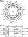
- the first system excitation winding 10A, the first system two output windings 111A, 112A, the second system excitation winding 10B, and the second system two output windings 111B, 112B are wound around the same one stator 13.
- the rotor 14 is arranged in the radial-direction inner side of the stator 13.
- the rotor 14 is provided with a plurality of projection parts which are arranged equally in the circumferential direction on the peripheral part of the rotor.
- the projection height to the radial-direction outside of the projection parts is formed so that the gap permeance between the stator 13 and the rotor 14 changes in sine wave shape according to rotation.
- the resolver 1 is a variable reluctance (VR) type resolver.
- the five projection parts are provided, and the axial double angle is 5. Therefore, whenever the rotor rotates once in the mechanical angle, it rotates 5 times in the electrical angle.
- the amplitude of AC voltage V1A induced by the first system first output winding 111A and the amplitude of AC voltage V2A induced by the first system second output winding 112A change in a sine wave shape (or in a cosine wave shape), according to the rotational angle (the gap permeance) in the electrical angle of the rotor.
- the first system first output winding 111A and the first system second output winding 112A are wound around the positions of the circumferential direction of the stator 13 so that the amplitudes of those AC voltages are mutually different 90 degrees in the electrical angle.
- the second system first output winding 111B and the second system second output winding 112B are wound around the positions of the circumferential direction of the stator 13 so that the amplitudes of those induced AC voltages are mutually different 90 degrees in the electrical angle.
- the stator 13 is provided with 12 teeth arranged equally in the circumferential direction; the first system windings are wound around the first teeth TE1 to the sixth teeth TE6; and the second system windings are wound around the seventh teeth TE7 to the twelfth teeth TE12.
- the first system excitation winding 10A is distributed and wound around the first teeth TE1 to the sixth teeth TE6.
- the first system first output winding 111A and the first system second output winding 112A are distributed and wound around the first teeth TE1 to the sixth teeth TE6 so that the amplitudes of those induced AC voltages are mutually different 90 degrees in the electrical angle.
- the second system excitation winding 10B is distributed and wound around the seventh teeth TE7 to the twelfth teeth TE12.
- the second system first output winding 111B and the second system second output winding 112B are distributed and wound around the seventh teeth TE7 to the twelfth teeth TE12 so that the amplitudes of those induced AC voltages are mutually different 90 degrees in the electrical angle.
- the first system excitation winding 10A wound around the plurality of teeth is connected in series between teeth; and the two terminals of the first system excitation winding 10A connected in series are connected to the controller 50 (the first system excitation unit 51A) described below.
- the two terminals of the first system first output winding 111A connected in series between teeth are connected to the controller 50 (the first system output signal detection unit 52A) described below.
- the two terminals of the first system second output winding 112A connected in series between teeth are connected to the controller 50 (the first system output signal detection unit 52A) described below.
- the two terminals of the second system excitation winding 10B connected in series are connected to the controller 50 (the second system excitation unit 51B) described below.
- the two terminals of the second system first output winding 111B connected in series between teeth are connected to the controller 50 (the second system output signal detection unit 52B) described below.
- the two terminals of the second system second output winding 112B connected in series between teeth are connected to the controller 50 (the second system output signal detection unit 52B) described below.
- the number of projection parts (axial double angle) and the number of teeth may be set to any numbers.
- the first system windings and the second system windings may not be arranged being divided into two in the circumferential direction, but may be arranged being distributed in the circumferential direction.
- the angle detection apparatus is provided with a controller 50.
- the controller 50 is provided with a first system excitation unit 51A, a first system output signal detection unit 52A, a first system removal processing unit 53A, a first system angle calculation unit 54A, a second system excitation unit 51B, a second system output signal detection unit 52B, a second system removal processing unit 53B, and a second system angle calculation unit 54B.
- Each function of the controller 50 is realized by processing circuits provided in the controller 50. Specifically, as shown in FIG.
- the controller 50 is provided with, as a processing circuit, an arithmetic processor (computer) 90 such as a CPU (Central Processing Unit), storage apparatuses 91 that exchange data with the arithmetic processor 90, an input circuit 92 that inputs external signals to the arithmetic processor 90, an output circuit 93 that outputs signals from the arithmetic processor 90 to the outside, and the like.
- an arithmetic processor computer
- CPU Central Processing Unit
- ASIC Application Specific Integrated Circuit
- IC Integrated Circuit
- DSP Digital Signal Processor
- FPGA Field Programmable Gate Array
- various kinds of logical circuits various kinds of signal processing circuits, and the like
- the arithmetic processor 90 a plurality of the same type ones or the different type ones may be provided, and each processing may be shared and executed.
- the storage apparatuses 91 there are provided a RAM (Random Access Memory) which can read data and write data from the arithmetic processor 90, a ROM (Read Only Memory) which can read data from the arithmetic processor 90, and the like.
- the first system first output winding 111A, the first system second output winding 112A, the second system first output winding 111B, and the second system second output winding 112B are connected to the input circuit 92.
- the input circuit 92 is provided with an A/D converter and the like for inputting the output voltages of these windings into the arithmetic processor 90.
- the output circuit 93 is connected with the first system excitation winding 10A and the second system excitation winding 10B, and is provided with driving circuits, such as switching devices for applying the AC voltage VRA to these windings.
- a lowpass filter circuit may be provided in the output side of the switching device.
- the output circuit 93 is provided with signal output circuits, such as a communication circuit which transmits the first angle ⁇ 1 and the second angle ⁇ 2 which were calculated to the external controller 94.
- the arithmetic processor 90 runs software items (programs) stored in the storage apparatus 91 such as a ROM and collaborates with other hardware devices in the controller 50, such as the storage apparatus 91, the input circuit 92, and the output circuit 93, so that the respective functions of the control units 51A to 54B included in the controller 50 are realized.
- Setting data utilized in the control units 51A to 54B are stored, as part of software items (programs), in the storage apparatus 91 such as a ROM.
- Each function of the controller 50 will be described in detail below.
- the first system excitation unit 51A applies AC voltage VRA (in this example, AC voltage VRA of a sine wave) of first cycle TA to the first system excitation winding 10A.
- the first system excitation unit 51A calculates an AC voltage command of the first cycle TA, and generates the PWM signal (Pulse Width Modulation) which turns on and off the switching device for the first system excitation winding provided in the output circuit 93, based on the comparison result between the AC voltage command and the triangular wave.
- the switching device is turned on, the power source voltage is applied to the first system excitation winding 10A side, and when the switching device is turned off, the application of the power source voltage stops.
- the second system excitation unit 51B applies AC voltage VRB (in this example, AC voltage VRB of a sine wave) of second cycle TB to the second system excitation winding 10B.
- the second cycle TB is set to a cycle longer than the first cycle TA.
- the second system excitation unit 51B calculates an AC voltage command of the second cycle TB, and generates the PWM signal (Pulse Width Modulation) which turns on and off the switching device for the second system excitation winding provided in the output circuit 93, based on the comparison result between the AC voltage command and the triangular wave.
- PWM signal Pulse Width Modulation
- the first system output signal detection unit 52A detects periodically the output signals V1A, V2A of the first system two output windings 111A, 112A at preliminarily set detection timing (hereinafter, referred to also as the first system detection timing).
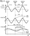
- the components of the second cycle V1A_TB, V2A_TB induced by the magnetic flux of the second cycle TB excited in the second system excitation winding 10B are superimposed on each of the output signals V1A, V2A of the first system two output windings 111A, 112A, due to the magnetic interference between systems.
- the output signal V1A of the first system first output winding is shown in the upper row graph of FIG.
- the component of the first cycle V1A_TA induced by the magnetic flux of the first system excitation winding 10A included in the output signal V1A of the first system first output winding is shown in the middle graph; and the component of the second cycle V1A_TB induced by the magnetic flux of the second system excitation winding 10B included in the output signal V1A of the first system first output winding is shown in the lower row graph.
- the output signal V1A of the first system first output winding becomes a signal obtained by totaling the component of the first cycle V1A_TA and the component of the second cycle V1A_TB, and if the angle is calculated with these signals, the detection error will occur. Therefore, in order to suppress the detection error of the angle, it is necessary to remove the component of the second cycle V1A_TB from the output signal V1A of the first system first output winding.
- the first system removal processing unit 53A performs a second cycle component removal processing which removes (decreases) the component of the second cycle, to the detection values V1A_S, V2A_S of the output signals of the first system two output windings.
- the first system angle calculation unit 54A calculates the first angle ⁇ 1 based on the detection values V1A_F, V2A_F of the output signals of the first system two output windings after the second cycle component removal processing.
- the second cycle component removal processing is performed.
- the phase is reversed and the sign of plus or minus is reversed in a cycle (for example, half cycle TB/2 of the second cycle) obtained by adding an integral multiple of the second cycle TB to a half cycle TB/2 of the second cycle.
- the first system removal processing unit 53A adds the detection values V1A_S, V2A_S of the output signals of the first system two output windings detected at this time detection timing, and the detection values V1A_Sold, V2A_Sold of the output signals of the first system two output windings detected at the detection timing earlier by the first system removal processing interval ⁇ T1 than this time detection timing.
- the first system removal processing interval ⁇ T1 is set as shown in the next equation.
- M is an integer greater than or equal to 0.
- M is set to 0, and the first system removal processing interval ⁇ T1 is set to the half cycle TB/2 of the second cycle.
- ⁇ T 1 TB/ 2 + TB ⁇ M
- the first system removal processing unit 53A is constituted, for example, as shown in FIG. 5 .
- the first system removal processing unit 53A is provided with a first delay device 53A1 which delays the detection value V1A_S of the output signal of the first system first output winding by the first system removal processing interval ⁇ T1, and outputs; adds the detection value V1A_S of the output signal of the first system first output winding, and the output V1A_Sold of the first delay device 53A1; and calculates the detection value V1A_F of the output signal of the first system first output winding after the second cycle component removal processing.
- the first system removal processing unit 53A is provided with a second delay device 53A2 which delays the detection value V2A_S of the output signal of the first system second output winding by the first system removal processing interval ⁇ T1, and outputs; adds the detection value V2A_S of the output signal of the first system second output winding, and the output V2A_Sold of the second delay device 53A2; and calculates the detection value V2A_F of the output signal of the first system second output winding after the second cycle component removal processing.
- a second delay device 53A2 which delays the detection value V2A_S of the output signal of the first system second output winding by the first system removal processing interval ⁇ T1, and outputs; adds the detection value V2A_S of the output signal of the first system second output winding, and the output V2A_Sold of the second delay device 53A2; and calculates the detection value V2A_F of the output signal of the first system second output winding after the second cycle component removal processing.
- the first system angle calculation unit 54A calculates the first angle ⁇ 1 based on the detection values V1A_F, V2A_F of the output signals of the first system two output windings after addition.
- the two components of the second cycle whose the signs of plus or minus are reversed with each other are added, and the two components of the second cycle are canceled with each other. Accordingly, in the detection values V1A_F, V2A_F of the output signals of the first system two output windings after addition, the component of the second cycle is removed. Then, based on the detection values after removing the component of the second cycle, the first angle ⁇ 1 can be calculated with good accuracy.
- the second cycle TB is set to an even multiple of the first cycle TA, as shown in the next equation.
- N is an integer greater than or equal to one.
- N is set to 1
- the second cycle TB is set to a twice of the first cycle TA.
- TB TA ⁇ 2 ⁇ N
- the first system removal processing interval ⁇ T1 becomes an integral multiple of the first cycle TA.
- ⁇ T 1 TA ⁇ N + 2 ⁇ N ⁇ M
- the detection values V1A_S, V2A_S of the output signals of the first system two output windings values before and after the integral multiple of the first cycle TA are added. Then, as shown in FIG. 4 , since the added two components of the first cycle have the same phase, and become the equivalent values with the same sign of plus or minus, the detection values V1A_F, V2A_F of the output signals of the first system two output windings after addition correspond to the double values of the components of the first cycle V1A_TA, V2A_TA included in the detection values, respectively.
- the first angle ⁇ 1 can be calculated with good accuracy.
- the first system removal processing unit 53A adds the detection values V1A_S, V2A_S of the output signals of the first system two output windings detected at this time detection timing, and the detection values V1A_Sold, V2A_Sold of the output signals of the first system two output windings detected before the first cycle TA (the half cycle TB/2 of the second cycle).
- the first system output signal detection unit 52A detects the output signals V1A, V2A of the first system two output windings at a timing when the AC voltage VRA of the first cycle TA applied to the first system excitation winding 10A becomes the maximum value or the minimum value (in this example, the maximum value).
- the first system output signal detection unit 52A detects the output signals V1A, V2A of the first system two output windings at every the first cycle TA when the AC voltage VRA becomes the maximum value. That is to say, the first system detection timing is set to the timing at every the first cycle TA.
- FIG. 6 shows an example in which unlike the present embodiment, there is no magnetic interference between systems, and the component of the second cycle is not superimposed on the output signals V1A, V2A of the first system two output windings.
- the output signals V1A, V2A of the first system two output windings are detected. Therefore, the component of the first cycle included in the detection values of the output signals of the first system two output windings becomes the maximum value or the minimum value of the component of the first cycle which is vibrating at the first cycle TA.
- the first system output signal detection unit 52A may detect the output signals V1A, V2A of the first system two output windings at the timing when the AC voltage VRA of the first cycle TA becomes other than the maximum value or the minimum value, excepting the timing when the AC voltage VRA of the first cycle TA becomes the vibration center value (node).
- the detection values V1A_S, V2A_S of the output signals of the first system two output windings become the sine wave and cosine wave which are mutually different 90 degrees in the electrical angle, and the first angle ⁇ 1 is calculated by calculating an arc tangent of a ratio of them. Even if there is the magnetic interference between systems, by using the detection values V1A_F, V2A_F of the output signals of the first system two output windings after the second cycle component removal processing, the first angle ⁇ 1 can be calculated.
- the first system angle calculation unit 54A calculates the first angle ⁇ 1 by calculating an arc tangent (an arc tangent function) of a ratio between the detection value V1A_F of the output signal of the first system first output winding and the detection value V2A_F of the output signal of the first system second output winding after the second cycle component removal processing.
- ⁇ 1 tan ⁇ 1 V 1 A _ F/V 2 A _ F
- the detection values V1A_F, V2A_F of the output signals of the first system two output windings after the second cycle component removal processing correspond to the double values of the components of the first cycle V1A_TA, V2A_TA included in the detection values, respectively. Therefore, as shown in a next equation in which the equation (4) is substituted in the equation (5), the first angle ⁇ 1 is calculated with good accuracy by the ratio of the components of the first cycle V1A_TA, V2A_TA included in the detection values.
- ⁇ 1 ⁇ tan ⁇ 1 2 ⁇ V 1 A _ TA / 2 ⁇ V 2 A _ TA tan ⁇ 1 V 1 A _ TA/V 2 A _ TA
- the second system output signal detection unit 52B detects periodically the output signal V1B, V2B of the second system two output windings 111B, 112B at preliminarily set detection timing (hereinafter, referred to also as the second system detection timing).
- the components of the first cycle induced by the magnetic flux of the first cycle TA excited in the first system excitation winding 10A are superimposed on each of the output signals V1B, V2B of the second system two output windings 111B, 112B, due to the magnetic interference between systems.
- the output signal V1B of the second system first output winding is shown in the upper row graph of FIG.
- the component of the second cycle V1B_TB induced by the magnetic flux of the second system excitation winding 10B included in the output signal V1B of the second system first output winding is shown in the middle graph; and the component of the first cycle V1B_TA induced by the magnetic flux of the first system excitation winding 10A included in the output signal V1B of the second system first output winding is shown in the lower row graph.
- the output signal V1B of the second system first output winding becomes a signal obtained by totaling the component of the second cycle V1B_TB and the component of the first cycle V1B_TA, and if the angle is calculated with these signals, the detection error will occur. Therefore, in order to suppress the detection error of the angle, it is necessary to remove the component of the first cycle V1B_TA from the output signal V1B of the second system first output winding.
- the second system removal processing unit 53B performs a first cycle component removal processing which removes (decreases) the component of the first cycle, to the detection values V1B_S, V2B_S of the output signals of the second system two output windings.
- the second system angle calculation unit 54B calculates the second angle ⁇ 2 based on the detection values V1B_F, V2B_F of the output signals of the second system two output windings after the first cycle component removal processing.
- the first cycle component removal processing is performed.
- the component of the first cycle V1B_TA of the output signal of the second system first output winding becomes the same phase and becomes the equivalent value with the same sign of plus or minus at an integral multiple cycle of the first cycle TA (for example, the first cycle TA).
- the second system removal processing unit 53B performs a subtraction processing that calculates differences between the detection values V1B_S, V2B_S of the output signals of the second system two output windings detected at this time detection timing, and the detection values V1B_Sold, V2B_Sold of the output signals of the second system two output windings detected at the detection timing earlier by the second system removal processing interval ⁇ T2 than this time detection timing.
- the second system removal processing interval ⁇ T2 is set to an integral multiple of the first cycle TA, as shown in a next equation.
- P is an integer greater than or equal to one. In the present embodiment, P is set to 1, and the second system removal processing interval ⁇ T2 is set to the first cycle TA.
- ⁇ T 2 TA ⁇ P
- the second system removal processing unit 53B is constituted, for example, as shown in FIG. 8 .
- the second system removal processing unit 53B is provided with a first delay device 53B1 which delays the detection value V1B_S of the output signal of the second system first output winding by the second system removal processing interval ⁇ T2, and outputs; subtracts the output V1B_Sold of the first delay device 53B1 from the detection value V1B_S of the output signal of the second system first output winding; and calculates the detection value V1B_F of the output signal of the second system first output winding after the first cycle component removal processing.
- the second system removal processing unit 53B is provided with a second delay device 53B2 which delays the detection value V2B_S of the output signal of the second system second output winding by the second system removal processing interval ⁇ T2, and outputs; subtracts the output V2B_Sold of the second delay device 53B2 from the detection value V2B_S of the output signal of the second system second output winding; and calculates the detection value V2B_F of the output signal of the second system second output winding after the first cycle component removal processing.
- a second delay device 53B2 which delays the detection value V2B_S of the output signal of the second system second output winding by the second system removal processing interval ⁇ T2, and outputs; subtracts the output V2B_Sold of the second delay device 53B2 from the detection value V2B_S of the output signal of the second system second output winding; and calculates the detection value V2B_F of the output signal of the second system second output winding after the first cycle component removal processing.
- the second system angle calculation unit 54B calculates the second angle ⁇ 2 based on the detection values V1B_F, V2B_F of the output signals of the second system two output windings after the subtraction processing.
- the two components of the first cycle which become the equivalent values with the same sign of plus or minus with each other are subtracted, and the two components of the first cycle are canceled with each other. Accordingly, in the detection values V1B_F, V2B_F of the output signals of the second system two output windings after the subtraction processing, the components of the first cycle are removed. Then, based on the detection values after removing the components of the first cycle, the second angle ⁇ 2 can be calculated with good accuracy.
- the second cycle TB is set to an even multiple of the first cycle TA, as shown in the next equation.
- N is an integer greater than or equal to one.
- N is set to 1
- the second cycle TB is set to the twice of the first cycle TA.
- the second system removal processing interval ⁇ T2 is set as shown in the next equation.
- L is an integer greater than or equal to 0.
- L is set to 0
- the second system removal processing interval ⁇ T2 is set to the half cycle TB/2 of the second cycle.
- ⁇ T 2 TB/ 2 + TB ⁇ L
- the detection values V1B_F, V2B_F of the output signals of the second system two output windings after the subtraction processing correspond to the double values of the components of the second cycle V1B_TB, V2B_TB included in the detection values, respectively.
- the second angle ⁇ 2 can be calculated with good accuracy.
- the second system removal processing unit 53B subtracts the detection values V1B_Sold, V2B_Sold of the output signals of the second system two output windings detected before the half cycle TB/2 of the second cycle (the first cycle TA), from the detection values V1B_S, V2B_S of the output signals of the second system two output windings detected at this time detection timing.
- the second system output signal detection unit 52B detects the output signals V1B, V2B of the second system two output windings at a timing when the AC voltage VRB of the second cycle TB applied to the second system excitation winding 10B becomes the maximum value or the minimum value.
- the second system output signal detection unit 52B detects the output signals V1B, V2B of the second system two output windings at every the half cycle TB/2 of the second cycle when the AC voltage VRB becomes the maximum value or the minimum value.
- the component of the second cycle included in the detection values of the output signals of the second system two output windings becomes the maximum value or the minimum value of the component of the second cycle which is vibrating at the second cycle TB. Therefore, the amplitude of the component of the second cycle included in the detection values of the output signals of the second system two output windings can be maximized, the detection sensitivity of the component of the second cycle to the noise component can be increased, and the detection accuracy can be increased.
- the second system output signal detection unit 52B may detect the output signals V1B, V2B of the second system two output windings at the timing when the AC voltage VRB of the second cycle TB becomes other than the maximum value or the minimum value, excepting the timing when the AC voltage VRB of the second cycle TB becomes the vibration center value (node).
- the second system angle calculation unit 54B calculates the second angle ⁇ 2 by calculating an arc tangent (an arc tangent function) of a ratio between the detection value V1B_F of the output signal of the second system first output winding and the detection value V2B_F of the output signal of the second system second output winding after the first cycle component removal processing.
- ⁇ 2 tan ⁇ 1 V1B _ F / V2B _ F
- the detection values V1B_F, V2B_F of the output signals of the second system two output windings after the first cycle component removal processing correspond to the double values of the components of the second cycle V1B_TB, V2B_TB included in the detection values, respectively. Therefore, as shown in a next equation in which the equation (11) is substituted in the equation (12), the second angle ⁇ 2 is calculated with good accuracy by the ratio of the components of the second cycle V1B_TB, V2B_TB included in the detection values.
- ⁇ 2 ⁇ tan ⁇ 1 2 ⁇ V1B _ TB / 2 ⁇ V2B _ TB tan ⁇ 1 V1B _ TB / V2B _ TB
- the setting values of the first cycle TA, the second cycle TB, the first system detection timing, the second system detection timing, the first system removal processing interval ⁇ T1, and the second system removal processing interval ⁇ T2 are preliminarily set to become the predetermined relation between the first system and the second system; the processing of the first system and the processing of the second system can be performed independently with each other; and it is not necessary to perform synchronous control in real time between the first system and the second system.
- Embodiment 2 Next, the angle detection apparatus according to Embodiment 2 will be explained. The explanation for constituent parts the same as those in Embodiment 1 will be omitted.
- the basic configuration of the angle detection apparatus according to the present embodiment is the same as that of Embodiment 1. But, the configuration of each second system processing units 51B to 54B of the controller 50 is different from that of Embodiment 1.
- the second system output signal detection unit 52B detects periodically the output signals V1B, V2B of the second system two output windings 111B, 112B at preliminarily set detection timing (the second system detection timing).
- the components of the first cycle induced by the magnetic flux of the first cycle TA excited in the first system excitation winding 10A are superimposed on each of the output signals V1B, V2B of the second system two output windings 111B, 112B, due to the magnetic interference between systems.
- the output signal V1B of the second system first output winding is shown in the upper row graph of FIG.
- the component of the second cycle V1B_TB induced by the magnetic flux of the second system excitation winding 10B included in the output signal V1B of the second system first output winding is shown in the middle graph; and the component of the first cycle V1B_TA induced by the magnetic flux of the first system excitation winding 10A included in the output signal V1B of the second system first output winding is shown in the lower row graph.
- the output signal V1B of the second system first output winding becomes a signal obtained by totaling the component of the second cycle V1B_TB and the component of the first cycle V1B_TA, and if the angle is calculated with these signals, the detection error will occur. Therefore, in order to suppress the detection error of the angle, it is necessary to remove the component of the first cycle V1B_TA from the output signal V1B of the second system first output winding.
- the second system removal processing unit 53B performs the first cycle component removal processing which removes the component of the first cycle, to the detection values V1B_S, V2B_S of the output signals of the second system two output windings. Then, the second system angle calculation unit 54B calculates the second angle ⁇ 2 based on the detection values V1B_F, V2B_F of the output signals of the second system two output windings after the first cycle component removal processing.
- the first cycle component removal processing is performed.
- the phase is reversed and the sign of plus or minus is reversed in a cycle (for example, half cycle TA/2 of the first cycle) obtained by adding an integral multiple of the first cycle TA to a half cycle TA/2 of the first cycle.
- the second system removal processing unit 53B adds the detection values V1B_S, V2B_S of the output signals of the second system two output windings detected at this time detection timing, and the detection values V1B_Sold, V2B_Sold of the output signals of the second system two output windings detected at the detection timing earlier by the second system removal processing interval ⁇ T2 than this time detection timing.
- the second system removal processing interval ⁇ T2 is set to an interval obtained by adding the integral multiple of the first cycle TA to the half cycle TA/2 of the first cycle, as shown in a next equation.
- X is an integer greater than or equal to 0.
- X is set to 0, and the second system removal processing interval ⁇ T2 is set to the half cycle TA/2 of the first cycle.
- ⁇ T2 TA / 2 + TA ⁇ X
- the second system angle calculation unit 54B calculates the second angle ⁇ 2 based on the detection values V1B_F, V2B_F of the output signals of the second system two output windings after addition.
- the two components of the first cycle whose the signs of plus or minus are reversed with each other are added, and the two components of the first cycle are canceled with each other. Accordingly, in the detection values V1B_F, V2B_F of the output signals of the second system two output windings after addition, the components of the first cycle are removed. Then, based on the detection values after removing the components of the first cycle, the second angle ⁇ 2 can be calculated with good accuracy.
- the second system output signal detection unit 52B detects periodically the output signals V1B, V2B of the second system two output windings at two timings TM1, TM2 which become before-and-after symmetrical with respect to a reference timing TM0 when the AC voltage VRB of the second cycle TB applied to the second system excitation winding 10B becomes the maximum value or the minimum value.
- the second system removal processing unit 53B adds the detection values of the output signals of the second system two output windings detected at the two timings TM1, TM2 which become before-and-after symmetry, with each other; and calculates the second angle ⁇ 2 based on the detection values V1B_F, V2B_F of the output signals of the second system two output windings after addition.
- the components of the second cycle included in the detection values of the output signals of the second system two output windings detected at two timings have the same phase, and become the equivalent values with the same sign of plus or minus. Since the interval between two timings TM1, TM2 is set to the second system removal processing interval ⁇ T2, in the components of the first cycle included in the detection values of the output signals of the second system two output windings detected at two timings TM1, TM2, the phases are reversed and the signs of plus or minus are reversed.
- the detection values V1B_F, V2B_F of the output signals of the second system two output windings after addition correspond to the double values of the components of the second cycle V1B_TB, V2B_TB included in the detection values, respectively.
- the second angle ⁇ 2 can be calculated with good accuracy.
- the second system removal processing unit 53B is constituted, for example, as shown in FIG. 10 .
- the second system removal processing unit 53B is provided with a first delay device 53B1 which delays the detection value V1B_S of the output signal of the second system first output winding by the second system removal processing interval ⁇ T2, and outputs; adds the detection value V1B_S of the output signal of the second system first output winding and the output V1B_Sold of the first delay device 53B1, at the timing TM2 after the reference timing TM0; and calculates the detection value V1B_F of the output signal of the second system first output winding after the first cycle component removal processing.
- the second system removal processing unit 53B is provided with a second delay device 53B2 which delays the detection value V2B_S of the output signal of the second system second output winding by the second system removal processing interval ⁇ T2, and outputs; adds the detection value V2B_S of the output signal of the second system second output winding and the output V2B_Sold of the second delay device 53B2, at the timing TM2 after the reference timing TM0; and calculates the detection value V2B_F of the output signal of the second system second output winding after the first cycle component removal processing.
- the second cycle TB is set to twice of the first cycle TA.
- the second system removal processing interval ⁇ T2 is set to the half cycle TA/2 of the first cycle. Therefore, the interval ⁇ TM12 between each of before-and-after two timings TM1, TM2 and the reference timing TM0 is set to 1/4 of the first cycle TA/4.
- the second system output signal detection unit 52B detects the output signals V1B, V2B of the second system two output windings at every 1/4 of the second cycle TB/4; and each detection timing is set so as to become before-and-after symmetrical with respect to the reference timing TM0 when the AC voltage VRB of the second cycle TB becomes the maximum value or the minimum value.
- the second system angle calculation unit 54B calculates the second angle ⁇ 2 by calculating an arc tangent (an arc tangent function) of a ratio between the detection value V1B_F of the output signal of the second system first output winding and the detection value V2B_F of the output signal of the second system second output winding after the first cycle component removal processing.
- ⁇ 2 tan ⁇ 1 V1B _ F / V2B _ F
- the detection values V1B_F, V2B_F of the output signals of the second system two output windings after the first cycle component removal processing correspond to the double values of the components of the second cycle V1B_TB, V2B_TB included in the detection values, respectively. Therefore, as shown in a next equation in which the equation (16) is substituted in the equation (18), the second angle ⁇ 2 is calculated with good accuracy by the ratio of the components of the second cycle V1B_TB, V2B_TB included in the detection values.
- ⁇ 2 ⁇ tan ⁇ 1 2 ⁇ V1B _ TB / 2 ⁇ V2B _ TB tan ⁇ 1 V1B _ TB / V2B _ TB
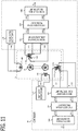
- FIG. 11 is a schematic configuration diagram of the angle detection apparatus according to the present embodiment.
- the resolver 1 is provided with the first system excitation winding 10A, the first system two output windings 111A, 112A, the second system excitation winding 10B, and the second system two output windings 111B, 112B.
- a magnetic interference occurs between the first system windings and the second system windings.
- the first system excitation winding 10A and the first system two output windings 111A, 112A are wound around the first system stator 13A; and the second system excitation winding 10B and the second system two output windings 111B, 112B are wound around the second system stator 13B.
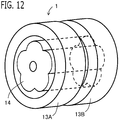
- the first system stator 13A and the second system stator 13B are arranged adjacent to each other in the axial direction; and a magnetic interference occurs between the first system windings and the second system windings.
- the teeth and the windings of the first system stator 13A, and the teeth and the windings of the second system stator 13B are omitted in figure.
- the first system stator 13A and the second system stator 13B are coaxially arranged adjacent to each other in the axial direction; and the rotor 14 formed integrally is arranged in the radial-direction inner side of the first system stator 13A and the second system stator 13B.
- the rotor 14 is provided with a plurality of projection parts which are arranged equally in the circumferential direction on the peripheral part of the rotor.
- the rotor part located in the radial-direction inner side of the first system stator 13A and the rotor part located in the radial-direction inner side of the second system stator 13B have the same shape of the projection parts.
- the rotor part of the radial-direction inner side of the first system stator 13A and the rotor part of the radial-direction inner side of the second system stator 13B may have the different shapes and the different numbers of the projection parts with each other; and these may be the different bodies connected so as to rotate integrally.
- the first system stator 13A is provided with a plurality of teeth arranged equally in the circumferential direction.
- the first system first output winding 111A and the first system second output winding 112A are distributed and wound around each teeth of the first system stator 13A so that the amplitudes of those induced AC voltages are mutually different 90 degrees in the electrical angle.
- the first system excitation winding 10A is distributed and wound around each teeth of the first system stator 13A.
- the second system stator 13B is provided with a plurality of teeth arranged equally in the circumferential direction.
- the second system first output winding 111B and the second system second output winding 112B are distributed and wound around each teeth of the second system stator 13B so that the amplitudes of those induced AC voltages are mutually different 90 degrees in the electrical angle.
- the second system excitation winding 10B is distributed and wound around each teeth of the second system stator 13B.
- the teeth number of the first system stator 13A and the teeth number of the second system stator 13B may be the same numbers, or may be the different numbers.
Landscapes
- Physics & Mathematics (AREA)
- General Physics & Mathematics (AREA)
- Transmission And Conversion Of Sensor Element Output (AREA)
- Measurement Of Length, Angles, Or The Like Using Electric Or Magnetic Means (AREA)
Abstract
Description
- The present disclosure relates to an angle detection apparatus.
- As the angle detection device which detects the rotational angle of the motor, the resolver is used well. Although the resolver is known as the robust angle detection device, the resolver is also required for redundancy from the request of the fault tolerance of the motor drive system.
- Then, PLT 1 discloses the dual system resolver which is provided with the first system excitation winding and output winding, and the second system excitation winding and output winding. In
PLT 2, two resolvers are excited asynchronous with each other by two magnetizing means, and the rotational angle of each resolver is calculated based on the sampling result of each resolver output sampled at each predetermined sampling cycle. In the technology ofPLT 2, the excitation frequency of each resolver by the two magnetizing means and the sampling frequency for sampling the output of each resolver are set so that the difference of the excitation frequency between resolvers becomes an integral multiple of the sampling frequency. And, the output of each resolver excited by the two magnetizing means is sampled at the peak timings of output amplitude. It is described inPLT 2 that since the sampling of each resolver output is always performed at the peak timings of output amplitude, the rotational angle is always calculated uniformly with high accuracy. -
- PLT 1:
JP 2000-18968 A - PLT 2:
JP 2009-210281 A - However, in the redundant system resolver like PLT 1 and PLT 2, even if electrically insulated between the first system and the second system, a magnetic interference occurs. Against this, in the technology of
PLT 2, after calculating the difference between the excitation frequency fa of the first system, and the excitation frequency fb of the second system by the pulsation cycle calculation unit, the sampling frequencies of the first system and the second system are adjusted by the sampling timing controller. Therefore, in the technology ofPLT 2, it is necessary to communicate between the first system ECU and the second system ECU and perform synchronous control. The harness cost and the processing load required for this communication between the first system and the second system, and the synchronous control becomes a problem. - Thus, even using the redundant system resolver in which the magnetic interference between systems occurs, it is desirable to provide an angle detection apparatus which can reduces the influence of the magnetic interference and can calculate the rotational angle with good accuracy, without performing synchronous control between systems in real time.
- An angle detection apparatus according to the present disclosure including:
- a resolver that is provided with a first system excitation winding, first system two output windings, a second system excitation winding, and second system two output windings, in which magnetic interference occurs between a first system and a second system;
- a first system excitation unit that applies AC voltage of a first cycle to the first system excitation winding;
- a second system excitation unit that applies AC voltage of a second cycle longer than the first cycle, to the second system excitation winding;
- a first system output signal detection unit that detects periodically output signals of the first system two output windings at preliminarily set detection timing;
- a first system removal processing unit that performs a second cycle component removal processing which removes component of the second cycle, to detection values of the output signals of the first system two output windings; and
- a first system angle calculation unit that calculates a first angle of the resolver, based on the detection values of the output signals of the first system two output windings after the second cycle component removal processing.
- According to the angle detection apparatus of the present disclosure, the component of the second cycle generated by the second system excitation winding can be removed from the detection values of the output signals of the first system two output windings. And, the angle of the rotor can be calculated with good accuracy, based on the detection values of the output signals of the first system two output windings after the second cycle component removal processing. At this time, it is not necessary to perform a synchronous control with processing of the second system in real time, and the increase in processing load and the like can be suppressed.
-
-
FIG. 1 is a schematic configuration diagram of the angle detection apparatus according toEmbodiment 1; -
FIG. 2 is a side view of the resolver viewed in the axial direction according toEmbodiment 1; -
FIG. 3 is a hardware configuration diagram of the controller according toEmbodiment 1; -
FIG. 4 is a time chart for explaining the second cycle component removal processing of the first system according toEmbodiment 1; -
FIG. 5 is a block diagram of the first system removal processing unit according toEmbodiment 1; -
FIG. 6 is a time chart for explaining the first system detection timing when supposing that there is no magnetic interference between systems according toEmbodiment 1; -
FIG. 7 is a time chart for explaining the first cycle component removal processing of the second system according toEmbodiment 1; -
FIG. 8 is a block diagram of the second system removal processing unit according toEmbodiment 1; -
FIG. 9 is a time chart for explaining the first cycle component removal processing of the second system according toEmbodiment 2; -
FIG. 10 is a block diagram of the second system removal processing unit according toEmbodiment 2; -
FIG. 11 is a schematic configuration diagram of the angle detection apparatus according to Embodiment 3; and -
FIG. 12 is a schematic perspective view of the resolver according to Embodiment 3. - An angle detection apparatus according to
Embodiment 1 will be explained with reference to drawings.FIG. 1 is a schematic configuration diagram of the angle detection apparatus according to the present embodiment. - The angle detection apparatus is provided with a
resolver 1. Theresolver 1 is provided with a first system excitation winding 10A, first system twooutput windings output windings output windings output windings output windings output windings - As shown in
FIG. 2 , the first system excitation winding 10A, the first system twooutput windings output windings stator 13. Therotor 14 is arranged in the radial-direction inner side of thestator 13. Therotor 14 is provided with a plurality of projection parts which are arranged equally in the circumferential direction on the peripheral part of the rotor. The projection height to the radial-direction outside of the projection parts is formed so that the gap permeance between thestator 13 and therotor 14 changes in sine wave shape according to rotation. That is to say, theresolver 1 is a variable reluctance (VR) type resolver. In the present embodiment, the five projection parts are provided, and the axial double angle is 5. Therefore, whenever the rotor rotates once in the mechanical angle, it rotates 5 times in the electrical angle. - As showing an example supposed that there is no magnetic interference between systems in
FIG. 6 , when the rotor rotates in the state where the AC voltage VRA is applied to the first system excitation winding 10A, the amplitude of AC voltage V1A induced by the first system first output winding 111A and the amplitude of AC voltage V2A induced by the first system second output winding 112A change in a sine wave shape (or in a cosine wave shape), according to the rotational angle (the gap permeance) in the electrical angle of the rotor. The first system first output winding 111A and the first system second output winding 112A are wound around the positions of the circumferential direction of thestator 13 so that the amplitudes of those AC voltages are mutually different 90 degrees in the electrical angle. Similarly, the second system first output winding 111B and the second system second output winding 112B are wound around the positions of the circumferential direction of thestator 13 so that the amplitudes of those induced AC voltages are mutually different 90 degrees in the electrical angle. - In the present embodiment, as shown in
FIG. 2 , thestator 13 is provided with 12 teeth arranged equally in the circumferential direction; the first system windings are wound around the first teeth TE1 to the sixth teeth TE6; and the second system windings are wound around the seventh teeth TE7 to the twelfth teeth TE12. The first system excitation winding 10A is distributed and wound around the first teeth TE1 to the sixth teeth TE6. The first system first output winding 111A and the first system second output winding 112A are distributed and wound around the first teeth TE1 to the sixth teeth TE6 so that the amplitudes of those induced AC voltages are mutually different 90 degrees in the electrical angle. Similarly, the second system excitation winding 10B is distributed and wound around the seventh teeth TE7 to the twelfth teeth TE12. The second system first output winding 111B and the second system second output winding 112B are distributed and wound around the seventh teeth TE7 to the twelfth teeth TE12 so that the amplitudes of those induced AC voltages are mutually different 90 degrees in the electrical angle. - The first system excitation winding 10A wound around the plurality of teeth is connected in series between teeth; and the two terminals of the first system excitation winding 10A connected in series are connected to the controller 50 (the first
system excitation unit 51A) described below. Similarly, the two terminals of the first system first output winding 111A connected in series between teeth are connected to the controller 50 (the first system outputsignal detection unit 52A) described below. The two terminals of the first system second output winding 112A connected in series between teeth are connected to the controller 50 (the first system outputsignal detection unit 52A) described below. The two terminals of the second system excitation winding 10B connected in series are connected to the controller 50 (the secondsystem excitation unit 51B) described below. Similarly, the two terminals of the second system first output winding 111B connected in series between teeth are connected to the controller 50 (the second system outputsignal detection unit 52B) described below. The two terminals of the second system second output winding 112B connected in series between teeth are connected to the controller 50 (the second system outputsignal detection unit 52B) described below. - The number of projection parts (axial double angle) and the number of teeth may be set to any numbers. The first system windings and the second system windings may not be arranged being divided into two in the circumferential direction, but may be arranged being distributed in the circumferential direction.
- The angle detection apparatus is provided with a
controller 50. As shown inFIG. 1 , thecontroller 50 is provided with a firstsystem excitation unit 51A, a first system outputsignal detection unit 52A, a first systemremoval processing unit 53A, a first systemangle calculation unit 54A, a secondsystem excitation unit 51B, a second system outputsignal detection unit 52B, a second systemremoval processing unit 53B, and a second systemangle calculation unit 54B. Each function of thecontroller 50 is realized by processing circuits provided in thecontroller 50. Specifically, as shown inFIG. 3 , thecontroller 50 is provided with, as a processing circuit, an arithmetic processor (computer) 90 such as a CPU (Central Processing Unit),storage apparatuses 91 that exchange data with thearithmetic processor 90, aninput circuit 92 that inputs external signals to thearithmetic processor 90, anoutput circuit 93 that outputs signals from thearithmetic processor 90 to the outside, and the like. - As the
arithmetic processor 90, ASIC (Application Specific Integrated Circuit), IC (Integrated Circuit), DSP (Digital Signal Processor), FPGA (Field Programmable Gate Array), various kinds of logical circuits, various kinds of signal processing circuits, and the like may be provided. As thearithmetic processor 90, a plurality of the same type ones or the different type ones may be provided, and each processing may be shared and executed. As thestorage apparatuses 91, there are provided a RAM (Random Access Memory) which can read data and write data from thearithmetic processor 90, a ROM (Read Only Memory) which can read data from thearithmetic processor 90, and the like. The first system first output winding 111A, the first system second output winding 112A, the second system first output winding 111B, and the second system second output winding 112B are connected to theinput circuit 92. Theinput circuit 92 is provided with an A/D converter and the like for inputting the output voltages of these windings into thearithmetic processor 90. Theoutput circuit 93 is connected with the first system excitation winding 10A and the second system excitation winding 10B, and is provided with driving circuits, such as switching devices for applying the AC voltage VRA to these windings. A lowpass filter circuit may be provided in the output side of the switching device. Theoutput circuit 93 is provided with signal output circuits, such as a communication circuit which transmits the first angle θ1 and the second angle θ2 which were calculated to theexternal controller 94. - Then, the
arithmetic processor 90 runs software items (programs) stored in thestorage apparatus 91 such as a ROM and collaborates with other hardware devices in thecontroller 50, such as thestorage apparatus 91, theinput circuit 92, and theoutput circuit 93, so that the respective functions of thecontrol units 51A to 54B included in thecontroller 50 are realized. Setting data utilized in thecontrol units 51A to 54B are stored, as part of software items (programs), in thestorage apparatus 91 such as a ROM. Each function of thecontroller 50 will be described in detail below. - The first
system excitation unit 51A applies AC voltage VRA (in this example, AC voltage VRA of a sine wave) of first cycle TA to the first system excitation winding 10A. In the present embodiment, the firstsystem excitation unit 51A calculates an AC voltage command of the first cycle TA, and generates the PWM signal (Pulse Width Modulation) which turns on and off the switching device for the first system excitation winding provided in theoutput circuit 93, based on the comparison result between the AC voltage command and the triangular wave. When the switching device is turned on, the power source voltage is applied to the first system excitation winding 10A side, and when the switching device is turned off, the application of the power source voltage stops. - The second
system excitation unit 51B applies AC voltage VRB (in this example, AC voltage VRB of a sine wave) of second cycle TB to the second system excitation winding 10B. As described later, the second cycle TB is set to a cycle longer than the first cycle TA. In the present embodiment, the secondsystem excitation unit 51B calculates an AC voltage command of the second cycle TB, and generates the PWM signal (Pulse Width Modulation) which turns on and off the switching device for the second system excitation winding provided in theoutput circuit 93, based on the comparison result between the AC voltage command and the triangular wave. - The first system output
signal detection unit 52A detects periodically the output signals V1A, V2A of the first system twooutput windings - As showing an example of the output signal V1A of the first system first output winding in
FIG. 4 , the components of the second cycle V1A_TB, V2A_TB induced by the magnetic flux of the second cycle TB excited in the second system excitation winding 10B are superimposed on each of the output signals V1A, V2A of the first system twooutput windings FIG. 4 ; the component of the first cycle V1A_TA induced by the magnetic flux of the first system excitation winding 10A included in the output signal V1A of the first system first output winding is shown in the middle graph; and the component of the second cycle V1A_TB induced by the magnetic flux of the second system excitation winding 10B included in the output signal V1A of the first system first output winding is shown in the lower row graph. The output signal V1A of the first system first output winding becomes a signal obtained by totaling the component of the first cycle V1A_TA and the component of the second cycle V1A_TB, and if the angle is calculated with these signals, the detection error will occur. Therefore, in order to suppress the detection error of the angle, it is necessary to remove the component of the second cycle V1A_TB from the output signal V1A of the first system first output winding. - Then, the first system
removal processing unit 53A performs a second cycle component removal processing which removes (decreases) the component of the second cycle, to the detection values V1A_S, V2A_S of the output signals of the first system two output windings. Then, the first systemangle calculation unit 54A calculates the first angle θ1 based on the detection values V1A_F, V2A_F of the output signals of the first system two output windings after the second cycle component removal processing. - In the present embodiment, based on the principle explained in the following, the second cycle component removal processing is performed. As shown in the lower row graph of
FIG. 4 , in the component of the second cycle V1A_TB of the output signal of the first system first output winding, the phase is reversed and the sign of plus or minus is reversed in a cycle (for example, half cycle TB/2 of the second cycle) obtained by adding an integral multiple of the second cycle TB to a half cycle TB/2 of the second cycle. - Then, as the second cycle component removal processing, the first system
removal processing unit 53A adds the detection values V1A_S, V2A_S of the output signals of the first system two output windings detected at this time detection timing, and the detection values V1A_Sold, V2A_Sold of the output signals of the first system two output windings detected at the detection timing earlier by the first system removal processing interval ΔT1 than this time detection timing. The first system removal processing interval ΔT1 is set as shown in the next equation. Herein, M is an integer greater than or equal to 0. In the present embodiment, M is set to 0, and the first system removal processing interval ΔT1 is set to the half cycle TB/2 of the second cycle.
- The first system
removal processing unit 53A is constituted, for example, as shown inFIG. 5 . The first systemremoval processing unit 53A is provided with a first delay device 53A1 which delays the detection value V1A_S of the output signal of the first system first output winding by the first system removal processing interval ΔT1, and outputs; adds the detection value V1A_S of the output signal of the first system first output winding, and the output V1A_Sold of the first delay device 53A1; and calculates the detection value V1A_F of the output signal of the first system first output winding after the second cycle component removal processing. Similarly, the first systemremoval processing unit 53A is provided with a second delay device 53A2 which delays the detection value V2A_S of the output signal of the first system second output winding by the first system removal processing interval ΔT1, and outputs; adds the detection value V2A_S of the output signal of the first system second output winding, and the output V2A_Sold of the second delay device 53A2; and calculates the detection value V2A_F of the output signal of the first system second output winding after the second cycle component removal processing. - Then, the first system
angle calculation unit 54A calculates the first angle θ1 based on the detection values V1A_F, V2A_F of the output signals of the first system two output windings after addition. - According to this configuration, the two components of the second cycle whose the signs of plus or minus are reversed with each other are added, and the two components of the second cycle are canceled with each other. Accordingly, in the detection values V1A_F, V2A_F of the output signals of the first system two output windings after addition, the component of the second cycle is removed. Then, based on the detection values after removing the component of the second cycle, the first angle θ1 can be calculated with good accuracy.
- In the present embodiment, the second cycle TB is set to an even multiple of the first cycle TA, as shown in the next equation. Herein, N is an integer greater than or equal to one. In the present embodiment, N is set to 1, and the second cycle TB is set to a twice of the first cycle TA.

- According to this configuration, as shown in the next equation in which the equation (2) is substituted in the equation (1), the first system removal processing interval ΔT1 becomes an integral multiple of the first cycle TA.

- Therefore, among the detection values V1A_S, V2A_S of the output signals of the first system two output windings, values before and after the integral multiple of the first cycle TA are added. Then, as shown in
FIG. 4 , since the added two components of the first cycle have the same phase, and become the equivalent values with the same sign of plus or minus, the detection values V1A_F, V2A_F of the output signals of the first system two output windings after addition correspond to the double values of the components of the first cycle V1A_TA, V2A_TA included in the detection values, respectively.
- Accordingly, in the equation (5) and the equation (6) described below, since 2 is canceled by calculating a ratio between the detection value V1A_F of the output signal of the first system first output winding after addition and the detection value V2A_F of the output signal of the first system second output winding after addition, the first angle θ1 can be calculated with good accuracy.
- In the present embodiment, M is set to 0, and N is set to 1. Therefore, the first system
removal processing unit 53A adds the detection values V1A_S, V2A_S of the output signals of the first system two output windings detected at this time detection timing, and the detection values V1A_Sold, V2A_Sold of the output signals of the first system two output windings detected before the first cycle TA (the half cycle TB/2 of the second cycle). - In the present embodiment, the first system output
signal detection unit 52A detects the output signals V1A, V2A of the first system two output windings at a timing when the AC voltage VRA of the first cycle TA applied to the first system excitation winding 10A becomes the maximum value or the minimum value (in this example, the maximum value). The first system outputsignal detection unit 52A detects the output signals V1A, V2A of the first system two output windings at every the first cycle TA when the AC voltage VRA becomes the maximum value. That is to say, the first system detection timing is set to the timing at every the first cycle TA. -
FIG. 6 shows an example in which unlike the present embodiment, there is no magnetic interference between systems, and the component of the second cycle is not superimposed on the output signals V1A, V2A of the first system two output windings. At every the first cycle TA when the AC voltage VRA of the first cycle TA becomes the maximum value, the output signals V1A, V2A of the first system two output windings are detected. Therefore, the component of the first cycle included in the detection values of the output signals of the first system two output windings becomes the maximum value or the minimum value of the component of the first cycle which is vibrating at the first cycle TA. Therefore, the amplitude of the component of the first cycle included in the detection values of the output signals of the first system two output windings can be maximized, the detection sensitivity of the component of the first cycle to the noise component can be increased, and the detection accuracy can be increased. The first system outputsignal detection unit 52A may detect the output signals V1A, V2A of the first system two output windings at the timing when the AC voltage VRA of the first cycle TA becomes other than the maximum value or the minimum value, excepting the timing when the AC voltage VRA of the first cycle TA becomes the vibration center value (node). - As shown in
FIG. 6 , if there is no magnetic interference between systems, the detection values V1A_S, V2A_S of the output signals of the first system two output windings become the sine wave and cosine wave which are mutually different 90 degrees in the electrical angle, and the first angle θ1 is calculated by calculating an arc tangent of a ratio of them. Even if there is the magnetic interference between systems, by using the detection values V1A_F, V2A_F of the output signals of the first system two output windings after the second cycle component removal processing, the first angle θ1 can be calculated. - In the present embodiment, as shown in a next equation, the first system
angle calculation unit 54A calculates the first angle θ1 by calculating an arc tangent (an arc tangent function) of a ratio between the detection value V1A_F of the output signal of the first system first output winding and the detection value V2A_F of the output signal of the first system second output winding after the second cycle component removal processing.
- As shown in the equation (4), the detection values V1A_F, V2A_F of the output signals of the first system two output windings after the second cycle component removal processing correspond to the double values of the components of the first cycle V1A_TA, V2A_TA included in the detection values, respectively. Therefore, as shown in a next equation in which the equation (4) is substituted in the equation (5), the first angle θ1 is calculated with good accuracy by the ratio of the components of the first cycle V1A_TA, V2A_TA included in the detection values.

- The second system output
signal detection unit 52B detects periodically the output signal V1B, V2B of the second system twooutput windings - As showing an example of the output signal V1B of the second system first output winding in
FIG. 7 , the components of the first cycle induced by the magnetic flux of the first cycle TA excited in the first system excitation winding 10A are superimposed on each of the output signals V1B, V2B of the second system twooutput windings FIG. 7 ; the component of the second cycle V1B_TB induced by the magnetic flux of the second system excitation winding 10B included in the output signal V1B of the second system first output winding is shown in the middle graph; and the component of the first cycle V1B_TA induced by the magnetic flux of the first system excitation winding 10A included in the output signal V1B of the second system first output winding is shown in the lower row graph. The output signal V1B of the second system first output winding becomes a signal obtained by totaling the component of the second cycle V1B_TB and the component of the first cycle V1B_TA, and if the angle is calculated with these signals, the detection error will occur. Therefore, in order to suppress the detection error of the angle, it is necessary to remove the component of the first cycle V1B_TA from the output signal V1B of the second system first output winding. - Then, the second system
removal processing unit 53B performs a first cycle component removal processing which removes (decreases) the component of the first cycle, to the detection values V1B_S, V2B_S of the output signals of the second system two output windings. Then, the second systemangle calculation unit 54B calculates the second angle θ2 based on the detection values V1B_F, V2B_F of the output signals of the second system two output windings after the first cycle component removal processing. - In the present embodiment, based on the principle explained in the following, the first cycle component removal processing is performed. As shown in the lower row graph of
FIG. 7 , the component of the first cycle V1B_TA of the output signal of the second system first output winding becomes the same phase and becomes the equivalent value with the same sign of plus or minus at an integral multiple cycle of the first cycle TA (for example, the first cycle TA). - Then, as the first cycle component removal processing, the second system
removal processing unit 53B performs a subtraction processing that calculates differences between the detection values V1B_S, V2B_S of the output signals of the second system two output windings detected at this time detection timing, and the detection values V1B_Sold, V2B_Sold of the output signals of the second system two output windings detected at the detection timing earlier by the second system removal processing interval ΔT2 than this time detection timing. The second system removal processing interval ΔT2 is set to an integral multiple of the first cycle TA, as shown in a next equation. Herein, P is an integer greater than or equal to one. In the present embodiment, P is set to 1, and the second system removal processing interval ΔT2 is set to the first cycle TA.
- The second system
removal processing unit 53B is constituted, for example, as shown inFIG. 8 . The second systemremoval processing unit 53B is provided with a first delay device 53B1 which delays the detection value V1B_S of the output signal of the second system first output winding by the second system removal processing interval ΔT2, and outputs; subtracts the output V1B_Sold of the first delay device 53B1 from the detection value V1B_S of the output signal of the second system first output winding; and calculates the detection value V1B_F of the output signal of the second system first output winding after the first cycle component removal processing. Similarly, the second systemremoval processing unit 53B is provided with a second delay device 53B2 which delays the detection value V2B_S of the output signal of the second system second output winding by the second system removal processing interval ΔT2, and outputs; subtracts the output V2B_Sold of the second delay device 53B2 from the detection value V2B_S of the output signal of the second system second output winding; and calculates the detection value V2B_F of the output signal of the second system second output winding after the first cycle component removal processing. - Then, the second system
angle calculation unit 54B calculates the second angle θ2 based on the detection values V1B_F, V2B_F of the output signals of the second system two output windings after the subtraction processing. - According to this configuration, the two components of the first cycle which become the equivalent values with the same sign of plus or minus with each other are subtracted, and the two components of the first cycle are canceled with each other. Accordingly, in the detection values V1B_F, V2B_F of the output signals of the second system two output windings after the subtraction processing, the components of the first cycle are removed. Then, based on the detection values after removing the components of the first cycle, the second angle θ2 can be calculated with good accuracy.
- In the present embodiment, the second cycle TB is set to an even multiple of the first cycle TA, as shown in the next equation. Herein, N is an integer greater than or equal to one. In the present embodiment, N is set to 1, and the second cycle TB is set to the twice of the first cycle TA.

- The second system removal processing interval ΔT2 is set as shown in the next equation. Herein, L is an integer greater than or equal to 0. In the present embodiment, L is set to 0, and the second system removal processing interval ΔT2 is set to the half cycle TB/2 of the second cycle.

- Even in this case, if the equation (8) is substituted in the equation (9), the second system removal processing interval ΔT2 becomes an integral multiple of the first cycle TA similarly to the equation (7), as shown in a next equation. Therefore, as mentioned above, by the first cycle component removal processing (the subtraction processing), the components of the first cycle can be removed.

- By setting the second system removal processing interval ΔT2 like the equation (9), in the two components of the second cycle which will be subtracted by the subtraction processing, the phases are reversed and the signs of plus or minus are reversed, as shown in
FIG. 7 . Therefore, the detection values V1B_F, V2B_F of the output signals of the second system two output windings after the subtraction processing correspond to the double values of the components of the second cycle V1B_TB, V2B_TB included in the detection values, respectively.
- Accordingly, in the equation (12) and the equation (13) described below, since 2 is canceled by calculating a ratio between the detection value V1B_F of the output signal of the second system first output winding after the subtraction processing and the detection value V2B_F of the output signal of the second system second output winding after the subtraction processing, the second angle θ2 can be calculated with good accuracy.
- In the present embodiment, L is set to 0, N is set to 1, and P is set to 1. Therefore, the second system
removal processing unit 53B subtracts the detection values V1B_Sold, V2B_Sold of the output signals of the second system two output windings detected before the half cycle TB/2 of the second cycle (the first cycle TA), from the detection values V1B_S, V2B_S of the output signals of the second system two output windings detected at this time detection timing. - In the present embodiment, the second system output
signal detection unit 52B detects the output signals V1B, V2B of the second system two output windings at a timing when the AC voltage VRB of the second cycle TB applied to the second system excitation winding 10B becomes the maximum value or the minimum value. The second system outputsignal detection unit 52B detects the output signals V1B, V2B of the second system two output windings at every the half cycle TB/2 of the second cycle when the AC voltage VRB becomes the maximum value or the minimum value. - According to this configuration, similar to the first system, the component of the second cycle included in the detection values of the output signals of the second system two output windings becomes the maximum value or the minimum value of the component of the second cycle which is vibrating at the second cycle TB. Therefore, the amplitude of the component of the second cycle included in the detection values of the output signals of the second system two output windings can be maximized, the detection sensitivity of the component of the second cycle to the noise component can be increased, and the detection accuracy can be increased. The second system output
signal detection unit 52B may detect the output signals V1B, V2B of the second system two output windings at the timing when the AC voltage VRB of the second cycle TB becomes other than the maximum value or the minimum value, excepting the timing when the AC voltage VRB of the second cycle TB becomes the vibration center value (node). - In the present embodiment, similar to the first system, as shown in a next equation, the second system
angle calculation unit 54B calculates the second angle θ2 by calculating an arc tangent (an arc tangent function) of a ratio between the detection value V1B_F of the output signal of the second system first output winding and the detection value V2B_F of the output signal of the second system second output winding after the first cycle component removal processing.
- As shown in the equation (11), the detection values V1B_F, V2B_F of the output signals of the second system two output windings after the first cycle component removal processing correspond to the double values of the components of the second cycle V1B_TB, V2B_TB included in the detection values, respectively. Therefore, as shown in a next equation in which the equation (11) is substituted in the equation (12), the second angle θ2 is calculated with good accuracy by the ratio of the components of the second cycle V1B_TB, V2B_TB included in the detection values.

- It is only required that the setting values of the first cycle TA, the second cycle TB, the first system detection timing, the second system detection timing, the first system removal processing interval ΔT1, and the second system removal processing interval ΔT2 are preliminarily set to become the predetermined relation between the first system and the second system; the processing of the first system and the processing of the second system can be performed independently with each other; and it is not necessary to perform synchronous control in real time between the first system and the second system.
- Next, the angle detection apparatus according to
Embodiment 2 will be explained. The explanation for constituent parts the same as those inEmbodiment 1 will be omitted. The basic configuration of the angle detection apparatus according to the present embodiment is the same as that ofEmbodiment 1. But, the configuration of each secondsystem processing units 51B to 54B of thecontroller 50 is different from that ofEmbodiment 1. - Also in the present embodiment, the second system output
signal detection unit 52B detects periodically the output signals V1B, V2B of the second system twooutput windings - As showing an example of the output signal V1B of the second system first output winding in
FIG. 9 , the components of the first cycle induced by the magnetic flux of the first cycle TA excited in the first system excitation winding 10A are superimposed on each of the output signals V1B, V2B of the second system twooutput windings FIG. 9 ; the component of the second cycle V1B_TB induced by the magnetic flux of the second system excitation winding 10B included in the output signal V1B of the second system first output winding is shown in the middle graph; and the component of the first cycle V1B_TA induced by the magnetic flux of the first system excitation winding 10A included in the output signal V1B of the second system first output winding is shown in the lower row graph. The output signal V1B of the second system first output winding becomes a signal obtained by totaling the component of the second cycle V1B_TB and the component of the first cycle V1B_TA, and if the angle is calculated with these signals, the detection error will occur. Therefore, in order to suppress the detection error of the angle, it is necessary to remove the component of the first cycle V1B_TA from the output signal V1B of the second system first output winding. - Also in the present embodiment, the second system
removal processing unit 53B performs the first cycle component removal processing which removes the component of the first cycle, to the detection values V1B_S, V2B_S of the output signals of the second system two output windings. Then, the second systemangle calculation unit 54B calculates the second angle θ2 based on the detection values V1B_F, V2B_F of the output signals of the second system two output windings after the first cycle component removal processing. - In the present embodiment, unlike
Embodiment 1, based on the principle explained in the following, the first cycle component removal processing is performed. As shown in the lower row graph ofFIG. 9 , in the component of the first cycle V1B_TA of the output signal of the second system first output winding, the phase is reversed and the sign of plus or minus is reversed in a cycle (for example, half cycle TA/2 of the first cycle) obtained by adding an integral multiple of the first cycle TA to a half cycle TA/2 of the first cycle. - Then, as the first cycle component removal processing, the second system
removal processing unit 53B adds the detection values V1B_S, V2B_S of the output signals of the second system two output windings detected at this time detection timing, and the detection values V1B_Sold, V2B_Sold of the output signals of the second system two output windings detected at the detection timing earlier by the second system removal processing interval ΔT2 than this time detection timing. The second system removal processing interval ΔT2 is set to an interval obtained by adding the integral multiple of the first cycle TA to the half cycle TA/2 of the first cycle, as shown in a next equation. Herein, X is an integer greater than or equal to 0. In the present embodiment, X is set to 0, and the second system removal processing interval ΔT2 is set to the half cycle TA/2 of the first cycle.
- Then, the second system
angle calculation unit 54B calculates the second angle θ2 based on the detection values V1B_F, V2B_F of the output signals of the second system two output windings after addition. - According to this configuration, the two components of the first cycle whose the signs of plus or minus are reversed with each other are added, and the two components of the first cycle are canceled with each other. Accordingly, in the detection values V1B_F, V2B_F of the output signals of the second system two output windings after addition, the components of the first cycle are removed. Then, based on the detection values after removing the components of the first cycle, the second angle θ2 can be calculated with good accuracy.
- In the present embodiment, as shown in
FIG. 9 , the second system outputsignal detection unit 52B detects periodically the output signals V1B, V2B of the second system two output windings at two timings TM1, TM2 which become before-and-after symmetrical with respect to a reference timing TM0 when the AC voltage VRB of the second cycle TB applied to the second system excitation winding 10B becomes the maximum value or the minimum value. - An interval between two timings which become before-and-after symmetry is set to the second system removal processing interval ΔT2. Therefore, as shown in a next equation, an interval ΔTM12 between each of before-and-after two timings TM1, TM2 and the reference timing TM0 is set to the half of the second system removal processing interval ΔT2.

- Then, the second system
removal processing unit 53B adds the detection values of the output signals of the second system two output windings detected at the two timings TM1, TM2 which become before-and-after symmetry, with each other; and calculates the second angle θ2 based on the detection values V1B_F, V2B_F of the output signals of the second system two output windings after addition. - According to this configuration, as shown in
FIG. 9 , the components of the second cycle included in the detection values of the output signals of the second system two output windings detected at two timings have the same phase, and become the equivalent values with the same sign of plus or minus. Since the interval between two timings TM1, TM2 is set to the second system removal processing interval ΔT2, in the components of the first cycle included in the detection values of the output signals of the second system two output windings detected at two timings TM1, TM2, the phases are reversed and the signs of plus or minus are reversed. Therefore, the detection values V1B_F, V2B_F of the output signals of the second system two output windings after addition correspond to the double values of the components of the second cycle V1B_TB, V2B_TB included in the detection values, respectively.
- Accordingly, in the equation (18) and the equation (19) described below, since 2 is canceled by calculating a ratio between the detection value V1B_F of the output signal of the second system first output winding after the addition processing and the detection value V2B_F of the output signal of the second system second output winding after the addition processing, the second angle θ2 can be calculated with good accuracy.
- The second system
removal processing unit 53B is constituted, for example, as shown inFIG. 10 . The second systemremoval processing unit 53B is provided with a first delay device 53B1 which delays the detection value V1B_S of the output signal of the second system first output winding by the second system removal processing interval ΔT2, and outputs; adds the detection value V1B_S of the output signal of the second system first output winding and the output V1B_Sold of the first delay device 53B1, at the timing TM2 after the reference timing TM0; and calculates the detection value V1B_F of the output signal of the second system first output winding after the first cycle component removal processing. Similarly, the second systemremoval processing unit 53B is provided with a second delay device 53B2 which delays the detection value V2B_S of the output signal of the second system second output winding by the second system removal processing interval ΔT2, and outputs; adds the detection value V2B_S of the output signal of the second system second output winding and the output V2B_Sold of the second delay device 53B2, at the timing TM2 after the reference timing TM0; and calculates the detection value V2B_F of the output signal of the second system second output winding after the first cycle component removal processing. - In the present embodiment, as shown in a next equation, the second cycle TB is set to twice of the first cycle TA. The second system removal processing interval ΔT2 is set to the half cycle TA/2 of the first cycle. Therefore, the interval ΔTM12 between each of before-and-after two timings TM1, TM2 and the reference timing TM0 is set to 1/4 of the first cycle TA/4.

- The second system output
signal detection unit 52B detects the output signals V1B, V2B of the second system two output windings at every 1/4 of the second cycle TB/4; and each detection timing is set so as to become before-and-after symmetrical with respect to the reference timing TM0 when the AC voltage VRB of the second cycle TB becomes the maximum value or the minimum value. - Similar to
Embodiment 1, as shown in a next equation, the second systemangle calculation unit 54B calculates the second angle θ2 by calculating an arc tangent (an arc tangent function) of a ratio between the detection value V1B_F of the output signal of the second system first output winding and the detection value V2B_F of the output signal of the second system second output winding after the first cycle component removal processing.
- As shown in the equation (16), the detection values V1B_F, V2B_F of the output signals of the second system two output windings after the first cycle component removal processing correspond to the double values of the components of the second cycle V1B_TB, V2B_TB included in the detection values, respectively. Therefore, as shown in a next equation in which the equation (16) is substituted in the equation (18), the second angle θ2 is calculated with good accuracy by the ratio of the components of the second cycle V1B_TB, V2B_TB included in the detection values.

- Next, the angle detection apparatus according to Embodiment 3 will be explained. The explanation for constituent parts the same as those in each of
Embodiments Embodiment 1. But, the configuration of theresolver 1 is different fromEmbodiment FIG. 11 is a schematic configuration diagram of the angle detection apparatus according to the present embodiment. - Similar to
Embodiment 1, theresolver 1 is provided with the first system excitation winding 10A, the first system twooutput windings output windings - However, in the present embodiment, unlike
Embodiment 1, as the schematic diagram of theresolver 1 is shown inFIG. 12 , the first system excitation winding 10A and the first system twooutput windings first system stator 13A; and the second system excitation winding 10B and the second system twooutput windings second system stator 13B. Thefirst system stator 13A and thesecond system stator 13B are arranged adjacent to each other in the axial direction; and a magnetic interference occurs between the first system windings and the second system windings. InFIG. 12 , the teeth and the windings of thefirst system stator 13A, and the teeth and the windings of thesecond system stator 13B are omitted in figure. - The
first system stator 13A and thesecond system stator 13B are coaxially arranged adjacent to each other in the axial direction; and therotor 14 formed integrally is arranged in the radial-direction inner side of thefirst system stator 13A and thesecond system stator 13B. Therotor 14 is provided with a plurality of projection parts which are arranged equally in the circumferential direction on the peripheral part of the rotor. In the present embodiment, the rotor part located in the radial-direction inner side of thefirst system stator 13A and the rotor part located in the radial-direction inner side of thesecond system stator 13B have the same shape of the projection parts. The rotor part of the radial-direction inner side of thefirst system stator 13A and the rotor part of the radial-direction inner side of thesecond system stator 13B may have the different shapes and the different numbers of the projection parts with each other; and these may be the different bodies connected so as to rotate integrally. - The
first system stator 13A is provided with a plurality of teeth arranged equally in the circumferential direction. The first system first output winding 111A and the first system second output winding 112A are distributed and wound around each teeth of thefirst system stator 13A so that the amplitudes of those induced AC voltages are mutually different 90 degrees in the electrical angle. The first system excitation winding 10A is distributed and wound around each teeth of thefirst system stator 13A. Thesecond system stator 13B is provided with a plurality of teeth arranged equally in the circumferential direction. The second system first output winding 111B and the second system second output winding 112B are distributed and wound around each teeth of thesecond system stator 13B so that the amplitudes of those induced AC voltages are mutually different 90 degrees in the electrical angle. The second system excitation winding 10B is distributed and wound around each teeth of thesecond system stator 13B. The teeth number of thefirst system stator 13A and the teeth number of thesecond system stator 13B may be the same numbers, or may be the different numbers. - Even using the configuration of this
kind resolver 1, by performing the similar processing as thecontroller 50 ofEmbodiment - Lastly, other embodiments of the present disclosure will be explained. Each of the configurations of embodiments to be explained below is not limited to be separately utilized but can be utilized in combination with the configurations of other embodiments as long as no discrepancy occurs.
-
- (1) In each of the above-mentioned Embodiments, there has been explained the case where the first system
removal processing unit 53A performs the addition processing of this time detection value and the detection value before the first system removal processing interval ΔT1, as the second cycle component removal processing which removes the component of the second cycle included in the detection values of the output signals of the first system two output windings; and the second systemremoval processing unit 53B performs the subtraction processing or the addition processing of this time detection value and the detection value before the second system removal processing interval ΔT2, as the first cycle component removal processing which removes the component of the first cycle included in the detection values of the output signals of second system two output windings. However, embodiments of the present disclosure are not limited to the foregoing case. That is to say, the first systemremoval processing unit 53A may perform a band elimination filter processing such as a high pass filter processing or a band stop filter processing which removes the component of the second cycle, as the second cycle component removal processing. The second systemremoval processing unit 53B may perform a band elimination filter processing such as a low pass filter processing or a band stop filter processing which removes the component of the first cycle, as the first cycle component removal processing. - (2) In each of the above-mentioned Embodiments, there been explained the case where the one
controller 50 is provided with theprocessing units 51A to 54A of the first system, and theprocessing units 51B to 54B of the second system. However, embodiments of the present disclosure are not limited to the foregoing case. That is to say, a controller of the first system may be provided with theprocessing units 51A to 54A of the first system, and a controller of the second system may be provided with theprocessing units 51B to 54B of the second system, or a plurality of controllers may be distributedly provided with eachprocessing units 51A to 54B of the first system and the second system. - (3) In each of the above-mentioned Embodiments, there has been explained the case where the first system output
signal detection unit 52A detects the output signals V1A, V2A of the first system two output windings at every the first cycle TA when the excitation AC voltage VRA becomes the maximum value. However, embodiments of the present disclosure are not limited to the foregoing case. That is to say, the first system outputsignal detection unit 52A may detect the output signals V1A, V2A of the first system two output windings at every the first cycle TA when the excitation AC voltage VRA becomes the minimum value, or may detect at every the first cycle TA when the AC voltage VRA becomes other than the maximum value and the minimum value, as mentioned above. Alternatively, the first system outputsignal detection unit 52A may detect at every half cycle TA/2 of the first cycle when the excitation AC voltage VRA becomes the maximum value or the minimum value. Alternatively, the first system outputsignal detection unit 52A may detect the output signals V1A, V2A of first system two output windings at every cycle which is different from the half cycle TA/2 of the first cycle and the first cycle TA (for example, a cycle obtained by dividing the first system removal processing interval ΔT1 by an integer greater than or equal to one). Also in these cases, the first delay device 53A1 and the second delay device 53A2 of the first systemremoval processing unit 53A delays the input signal by the first system removal processing interval ΔT1, and outputs. - (4) In the above-mentioned
Embodiment 1, there has been explained the case where the second system outputsignal detection unit 52B detects the output signals V1B, V2B of the second system two output windings at every the half cycle TB/2 of the second cycle when the excitation AC voltage VRB becomes the maximum value or the minimum value. However, embodiments of the present disclosure are not limited to the foregoing case. That is to say, as mentioned above, the second system outputsignal detection unit 52B may detect at every the half cycle TB/2 of the second cycle when the excitation AC voltage VRB becomes other than the maximum value and the minimum value. Alternatively, the second system outputsignal detection unit 52B may detect the output signals V1B, V2B of second system two output windings at every cycle which is different from the half cycle TB/2 of the second cycle (for example, a cycle obtained by dividing the second system removal processing interval ΔT2 by an integer greater than or equal to one). Also in these cases, the first delay device 53B1 and the second delay device 53B2 of the second systemremoval processing unit 53B delays the input signal by the second system removal processing interval ΔT2, and outputs. - (5) In the above-mentioned
Embodiment 2, there has been explained the case where the second system outputsignal detection unit 52B detects the output signals V1B, V2B of the second system two output windings at every 1/4 of the second cycle TB/4; and each detection timing is set so as to become before-and-after symmetrical with respect to the reference timing TM0 when the AC voltage VRB of the second cycle TB becomes the maximum value or the minimum value. However, embodiments of the present disclosure are not limited to the foregoing case. That is to say, the second system outputsignal detection unit 52B may detect periodically the output signals V1B, V2B of the second system two output windings at two timings which become before-and-after symmetrical with respect to the reference timing TM0 when the excitation AC voltage VRB becomes the maximum value. Alternatively, the second system outputsignal detection unit 52B may detect periodically the output signals V1B, V2B of the second system two output windings at two timings which become before-and-after symmetrical with respect to the reference timing TM0 when the excitation AC voltage VRB becomes the minimum value. As long as the interval between two timings which become before-and-after symmetry is set to the second system removal processing interval ΔT2, it may be set to an interval other than 1/4 of the second cycle TB/4. Also in these cases, the first delay device 53B1 and the second delay device 53B2 of the second systemremoval processing unit 53B delays the input signal by the second system removal processing interval ΔT2, and outputs. And, the second systemremoval processing unit 53B performs an addition processing at the timing TM2 after the reference timing TMθ, and calculates the detection values V1B_F, V2B_F of the output signals of the second system two output windings after addition. - (6) In each of the above-mentioned Embodiments, there has been explained the case where the first
system excitation unit 51A generates the PWM signal which turns on and off the switching device based on the comparison result between the AC voltage command and the triangular wave. However, embodiments of the present disclosure are not limited to the foregoing case. That is to say, the firstsystem excitation unit 51A may generate a rectangular wave signal of the first cycle TA which outputs binary voltage of the High level (for example, 5V) and Low level (for example, 0V) alternately by the driving circuit, its output may be inputted into a lowpass filter circuit, and the output of the lowpass filter circuit may be applied as the AC voltage VRA. - (7) In each of the above-mentioned Embodiments, there has been explained the case where the second
system excitation unit 51B generates the PWM signal which turns on and off the switching device based on the comparison result between the AC voltage command and the triangular wave. However, embodiments of the present disclosure are not limited to the foregoing case. That is to say, the secondsystem excitation unit 51B may generate a rectangular wave signal of the second cycle TB which outputs binary voltage of the High level (for example, 5V) and Low level (for example, 0V) alternately by the driving circuit, its output may be inputted into a lowpass filter circuit, and the output of the lowpass filter circuit may be applied as the AC voltage VRB. - Although the present disclosure is described above in terms of various exemplary embodiments and implementations, it should be understood that the various features, aspects and functionality described in one or more of the individual embodiments are not limited in their applicability to the particular embodiment with which they are described, but instead can be applied, alone or in various combinations to one or more of the embodiments. It is therefore understood that numerous modifications which have not been exemplified can be devised without departing from the scope of the present disclosure. For example, at least one of the constituent components may be modified, added, or eliminated. At least one of the constituent components mentioned in at least one of the preferred embodiments may be selected and combined with the constituent components mentioned in another preferred embodiment.
- 1 Resolver, 10A First system excitation winding, 10B Second system excitation winding, 111A First system first output winding, 112A First system second output winding, 111B Second system first output winding, 112B Second system second output winding, 50 Controller, 51A First system excitation unit, 52A First system output signal detection unit, 53A First system removal processing unit, 54A First system angle calculation unit, 51B Second system excitation unit, 52B Second system output signal detection unit, 53B Second system removal processing unit, 54B Second system angle calculation unit, θ1 First angle, θ2 Second angle, TA First cycle, TB Second cycle, ΔT1 First system removal processing interval, ΔT2 Second system removal processing interval, TM0 Reference timing, V1A_S Detection value of the output signal of the first system first output winding, V2A_S Detection value of the output signal of the first system second output winding, V1A_Sold Detection value of the output signal of the first system first output winding before the first system removal processing interval, V2A_Sold Detection value of the output signal of the first system second output winding before the first system removal processing interval, V1A_F Detection value of the output signal of the first system first output winding after the second cycle component removal processing, V2A_F Detection value of the output signal of the first system second output winding after the second cycle component removal processing, V1A_TA Component of the first cycle included in the output signal of the first system first output winding, V1A_TB Component of the second cycle included in the output signal of the first system first output winding, V2A_TA Component of the first cycle included in the output signal of the first system second output winding, V1B_S Detection value of the output signal of the second system first output winding, V2B_S Detection value of the output signal of the second system second output winding, V1B_Sold Detection value of the output signal of the second system first output winding before the second system removal processing interval, V2B_Sold Detection value of the output signal of the second system second output winding before the second system removal processing interval, V1B_F Detection value of the output signal of the second system first output winding after the first cycle component removal processing, V2B_F Detection value of the output signal of the second system second output winding after the first cycle component removal processing, V1B_TA Component of the first cycle included in the output signal of the second system first output winding, V1B_TB Component of the second cycle included in the output signal of the second system first output winding, V2B_TA Component of the first cycle included in the output signal of the second system second output winding
Claims (12)
- An angle detection apparatus comprising:a resolver that is provided with a first system excitation winding, first system two output windings, a second system excitation winding, and second system two output windings, in which magnetic interference occurs between a first system and a second system;a first system excitation unit that applies AC voltage of a first cycle to the first system excitation winding;a second system excitation unit that applies AC voltage of a second cycle longer than the first cycle, to the second system excitation winding;a first system output signal detection unit that detects periodically output signals of the first system two output windings at preliminarily set detection timing;a first system removal processing unit that performs a second cycle component removal processing which removes component of the second cycle, to detection values of the output signals of the first system two output windings; anda first system angle calculation unit that calculates a first angle of the resolver, based on the detection values of the output signals of the first system two output windings after the second cycle component removal processing.
- The angle detection apparatus according to claim 1,wherein the first system removal processing unit, as the second cycle component removal processing, adds the detection values of the output signals of the first system two output windings detected at this time detection timing, and the detection values of the output signals of the first system two output windings detected at the detection timing earlier by a first system removal processing interval than this time detection timing;wherein when setting the second cycle to TB, the first system removal processing interval is set to TB/2+TB×M (M is an integer greater than or equal to 0); andwherein the first system angle calculation unit calculates the first angle based on the detection values of the output signals of the first system two output windings after addition.
- The angle detection apparatus according to claim 2,
wherein when setting the first cycle to TA, the second cycle is set to TA×2×N (N is an integer greater than or equal to 1) . - The angle detection apparatus according to claim 2 or 3,
wherein the first system output signal detection unit detects the output signals of the first system two output windings at a timing when the AC voltage of the first cycle applied to the first system excitation winding becomes the maximum value or the minimum value. - The angle detection apparatus according to any one of claims 1 to 4, further comprising:a second system output signal detection unit that detects periodically output signals of the second system two output windings at preliminarily set detection timing;a second system removal processing unit that performs a first cycle component removal processing which removes component of the first cycle, to detection values of the output signals of the second system two output windings; anda second system angle calculation unit that calculates a second angle of the resolver, based on the detection values of the output signals of the second system two output windings after the first cycle component removal processing.
- The angle detection apparatus according to claim 5,wherein a second system removal processing unit, as the first cycle component removal processing, performs a subtraction processing which calculates differences between the detection values of the output signals of the second system two output windings detected at this time detection timing, and the detection values of the output signals of the second system two output windings detected at the detection timing earlier by a second system removal processing interval than this time detection timing;wherein when setting the first cycle to TA, the second system removal processing interval is set to TA×P (P is an integer greater than or equal to 1); andwherein the second system angle calculation unit calculates the second angle based on the detection values of the output signals of the second system two output windings after the subtraction processing.
- The angle detection apparatus according to claim 6,wherein when setting the first cycle to TA, the second cycle is set to TA×2×N (N is an integer greater than or equal to 1); andwherein when setting the second cycle to TB, the second system removal processing interval is set to TB/2+TB×L (L is an integer greater than or equal to 0).
- The angle detection apparatus according to claim 6 or 7,
wherein the second system output signal detection unit detects the output signals of the second system two output windings at a timing when the AC voltage of the second cycle applied to the second system excitation winding becomes the maximum value or the minimum value. - The angle detection apparatus according to claim 5,wherein the second system removal processing unit, as the first cycle component removal processing, adds the detection values of the output signals of the second system two output windings detected at this time detection timing, and the detection values of the output signals of the second system two output windings at the detection timing earlier by a second system removal processing interval than this time detection timing;wherein the second system angle calculation unit calculates the second angle based on the detection values of the output signals of the second system two output windings after addition; andwherein when setting the first cycle to TA, the second system removal processing interval is set to TA/2+TA×X (X is an integer greater than or equal to 0).
- The angle detection apparatus according to claim 9,wherein the second system output signal detection unit detects periodically the output signals of the second system two output windings at two timings which become before-and-after symmetrical with respect to a reference timing when the AC voltage of the second cycle applied to the second system excitation winding becomes the maximum value or the minimum value;wherein an interval between the two timings is set to the second system removal processing interval;wherein the second system removal processing unit adds the detection values of the output signals of the second system two output windings detected at each of the two timings with each other; andwherein the second system angle calculation unit calculates the second angle based on the detection values of the output signals of the second system two output windings after addition.
- The angle detection apparatus according to any one of claims 1 to 10,
wherein the first system excitation winding, the first system two output windings, the second system excitation winding, and the second system two output windings are wound around the same one stator. - The angle detection apparatus according to any one of claims 1 to 10,wherein the first system excitation winding and the first system two output windings are wound around a first system stator; andwherein the second system excitation winding and the second system two output windings are wound around a second system stator which adjoins the first system stator in an axial direction.
Applications Claiming Priority (1)
| Application Number | Priority Date | Filing Date | Title |
|---|---|---|---|
| PCT/JP2019/002395 WO2020152836A1 (en) | 2019-01-25 | 2019-01-25 | Angle detection device |
Publications (3)
| Publication Number | Publication Date |
|---|---|
| EP3916359A1 true EP3916359A1 (en) | 2021-12-01 |
| EP3916359A4 EP3916359A4 (en) | 2022-01-26 |
| EP3916359B1 EP3916359B1 (en) | 2023-08-30 |
Family
ID=71736905
Family Applications (1)
| Application Number | Title | Priority Date | Filing Date |
|---|---|---|---|
| EP19911129.5A Active EP3916359B1 (en) | 2019-01-25 | 2019-01-25 | Angle detection device |
Country Status (5)
| Country | Link |
|---|---|
| US (1) | US11828591B2 (en) |
| EP (1) | EP3916359B1 (en) |
| JP (1) | JP7026827B2 (en) |
| CN (1) | CN113330281B (en) |
| WO (1) | WO2020152836A1 (en) |
Families Citing this family (2)
| Publication number | Priority date | Publication date | Assignee | Title |
|---|---|---|---|---|
| WO2021157000A1 (en) * | 2020-02-06 | 2021-08-12 | 三菱電機株式会社 | Angle detection device |
| DE112022003256T5 (en) | 2021-06-25 | 2024-04-25 | Alps Alpine Co., Ltd. | POSITION DETECTION DEVICE |
Family Cites Families (12)
| Publication number | Priority date | Publication date | Assignee | Title |
|---|---|---|---|---|
| CN1068994C (en) * | 1996-11-05 | 2001-07-25 | 杨泰和 | Low Armature Response X-shaped Magnetic Circuit Structure of DC Motor |
| JP4157930B2 (en) * | 1998-07-06 | 2008-10-01 | 多摩川精機株式会社 | Duplex resolver |
| JP3871130B2 (en) * | 2003-03-19 | 2007-01-24 | 株式会社デンソー | Motor control device |
| JP4142607B2 (en) * | 2004-03-26 | 2008-09-03 | ミネベア株式会社 | Variable reluctance resolver |
| JP4729458B2 (en) | 2006-08-31 | 2011-07-20 | トヨタ自動車株式会社 | Rotation angle detector |
| JP5090847B2 (en) * | 2007-10-17 | 2012-12-05 | ミネベア株式会社 | Measuring device, signal processing method and program |
| JP2009210281A (en) | 2008-02-29 | 2009-09-17 | Toyota Motor Corp | Redundancy type rotating angle detection device |
| JP4991992B2 (en) | 2008-03-13 | 2012-08-08 | トヨタ自動車株式会社 | Resolver |
| JP2011257254A (en) * | 2010-06-09 | 2011-12-22 | Hitachi Automotive Systems Ltd | Rotation angle detection device |
| JP6005409B2 (en) | 2012-06-14 | 2016-10-12 | 日本航空電子工業株式会社 | Redundant resolver device |
| WO2016170588A1 (en) * | 2015-04-21 | 2016-10-27 | 株式会社日立製作所 | Magnetic field measurement system and failure diagnosis system using same |
| EP3399283B1 (en) * | 2015-12-28 | 2020-09-30 | Mitsubishi Electric Corporation | Rotation angle detecting device and dynamo-electric machine |
-
2019
- 2019-01-25 JP JP2020567324A patent/JP7026827B2/en active Active
- 2019-01-25 US US17/290,283 patent/US11828591B2/en active Active
- 2019-01-25 CN CN201980089736.1A patent/CN113330281B/en active Active
- 2019-01-25 EP EP19911129.5A patent/EP3916359B1/en active Active
- 2019-01-25 WO PCT/JP2019/002395 patent/WO2020152836A1/en not_active Ceased
Also Published As
| Publication number | Publication date |
|---|---|
| CN113330281B (en) | 2023-06-02 |
| JP7026827B2 (en) | 2022-02-28 |
| EP3916359A4 (en) | 2022-01-26 |
| CN113330281A (en) | 2021-08-31 |
| WO2020152836A1 (en) | 2020-07-30 |
| US11828591B2 (en) | 2023-11-28 |
| JPWO2020152836A1 (en) | 2021-05-20 |
| US20220018646A1 (en) | 2022-01-20 |
| EP3916359B1 (en) | 2023-08-30 |
Similar Documents
| Publication | Publication Date | Title |
|---|---|---|
| JP5148394B2 (en) | Microcomputer, motor control system | |
| EP3730903B1 (en) | Redundant resolver and rotation angle detection device using same | |
| EP4037181A1 (en) | Alternating-current rotating machine apparatus | |
| EP3916359B1 (en) | Angle detection device | |
| EP3396327B1 (en) | Rotation angle detector and torque sensor | |
| US20120197591A1 (en) | Angle detection apparatus | |
| US20200259447A1 (en) | Motor Controller | |
| EP4113069B1 (en) | Resolver abnormality detection device | |
| US9473054B2 (en) | Angle detection apparatus, motor driving control apparatus and angle detection method | |
| EP4113068B1 (en) | Abnormality detection device for resolver | |
| EP4102188B1 (en) | Angle detection device | |
| EP4134631A1 (en) | Redundant resolver and electric power steering device equipped with redundant resolver | |
| JP7186846B1 (en) | Control system for angle detector and AC rotating machine | |
| JP4840339B2 (en) | Control device | |
| JP2017195659A (en) | Electronic control device and motor control device | |
| JP2008058180A (en) | Rotation angle detector |
Legal Events
| Date | Code | Title | Description |
|---|---|---|---|
| STAA | Information on the status of an ep patent application or granted ep patent |
Free format text: STATUS: THE INTERNATIONAL PUBLICATION HAS BEEN MADE |
|
| PUAI | Public reference made under article 153(3) epc to a published international application that has entered the european phase |
Free format text: ORIGINAL CODE: 0009012 |
|
| STAA | Information on the status of an ep patent application or granted ep patent |
Free format text: STATUS: REQUEST FOR EXAMINATION WAS MADE |
|
| 17P | Request for examination filed |
Effective date: 20210521 |
|
| AK | Designated contracting states |
Kind code of ref document: A1 Designated state(s): AL AT BE BG CH CY CZ DE DK EE ES FI FR GB GR HR HU IE IS IT LI LT LU LV MC MK MT NL NO PL PT RO RS SE SI SK SM TR |
|
| A4 | Supplementary search report drawn up and despatched |
Effective date: 20220107 |
|
| RIC1 | Information provided on ipc code assigned before grant |
Ipc: G01D 3/08 20060101ALI20211223BHEP Ipc: G01D 5/244 20060101ALI20211223BHEP Ipc: G01B 7/30 20060101ALI20211223BHEP Ipc: G01D 5/20 20060101AFI20211223BHEP |
|
| DAV | Request for validation of the european patent (deleted) | ||
| DAX | Request for extension of the european patent (deleted) | ||
| GRAP | Despatch of communication of intention to grant a patent |
Free format text: ORIGINAL CODE: EPIDOSNIGR1 |
|
| STAA | Information on the status of an ep patent application or granted ep patent |
Free format text: STATUS: GRANT OF PATENT IS INTENDED |
|
| RIC1 | Information provided on ipc code assigned before grant |
Ipc: G01D 3/08 20060101ALI20230228BHEP Ipc: G01D 5/244 20060101ALI20230228BHEP Ipc: G01B 7/30 20060101ALI20230228BHEP Ipc: G01D 5/20 20060101AFI20230228BHEP |
|
| INTG | Intention to grant announced |
Effective date: 20230321 |
|
| P01 | Opt-out of the competence of the unified patent court (upc) registered |
Effective date: 20230424 |
|
| GRAS | Grant fee paid |
Free format text: ORIGINAL CODE: EPIDOSNIGR3 |
|
| GRAA | (expected) grant |
Free format text: ORIGINAL CODE: 0009210 |
|
| STAA | Information on the status of an ep patent application or granted ep patent |
Free format text: STATUS: THE PATENT HAS BEEN GRANTED |
|
| AK | Designated contracting states |
Kind code of ref document: B1 Designated state(s): AL AT BE BG CH CY CZ DE DK EE ES FI FR GB GR HR HU IE IS IT LI LT LU LV MC MK MT NL NO PL PT RO RS SE SI SK SM TR |
|
| REG | Reference to a national code |
Ref country code: GB Ref legal event code: FG4D |
|
| REG | Reference to a national code |
Ref country code: CH Ref legal event code: EP |
|
| REG | Reference to a national code |
Ref country code: DE Ref legal event code: R096 Ref document number: 602019036502 Country of ref document: DE |
|
| REG | Reference to a national code |
Ref country code: IE Ref legal event code: FG4D |
|
| REG | Reference to a national code |
Ref country code: LT Ref legal event code: MG9D |
|
| REG | Reference to a national code |
Ref country code: NL Ref legal event code: MP Effective date: 20230830 |
|
| REG | Reference to a national code |
Ref country code: AT Ref legal event code: MK05 Ref document number: 1605985 Country of ref document: AT Kind code of ref document: T Effective date: 20230830 |
|
| PG25 | Lapsed in a contracting state [announced via postgrant information from national office to epo] |
Ref country code: GR Free format text: LAPSE BECAUSE OF FAILURE TO SUBMIT A TRANSLATION OF THE DESCRIPTION OR TO PAY THE FEE WITHIN THE PRESCRIBED TIME-LIMIT Effective date: 20231201 |
|
| PG25 | Lapsed in a contracting state [announced via postgrant information from national office to epo] |
Ref country code: IS Free format text: LAPSE BECAUSE OF FAILURE TO SUBMIT A TRANSLATION OF THE DESCRIPTION OR TO PAY THE FEE WITHIN THE PRESCRIBED TIME-LIMIT Effective date: 20231230 |
|
| PG25 | Lapsed in a contracting state [announced via postgrant information from national office to epo] |
Ref country code: SE Free format text: LAPSE BECAUSE OF FAILURE TO SUBMIT A TRANSLATION OF THE DESCRIPTION OR TO PAY THE FEE WITHIN THE PRESCRIBED TIME-LIMIT Effective date: 20230830 Ref country code: RS Free format text: LAPSE BECAUSE OF FAILURE TO SUBMIT A TRANSLATION OF THE DESCRIPTION OR TO PAY THE FEE WITHIN THE PRESCRIBED TIME-LIMIT Effective date: 20230830 Ref country code: NO Free format text: LAPSE BECAUSE OF FAILURE TO SUBMIT A TRANSLATION OF THE DESCRIPTION OR TO PAY THE FEE WITHIN THE PRESCRIBED TIME-LIMIT Effective date: 20231130 Ref country code: LV Free format text: LAPSE BECAUSE OF FAILURE TO SUBMIT A TRANSLATION OF THE DESCRIPTION OR TO PAY THE FEE WITHIN THE PRESCRIBED TIME-LIMIT Effective date: 20230830 Ref country code: LT Free format text: LAPSE BECAUSE OF FAILURE TO SUBMIT A TRANSLATION OF THE DESCRIPTION OR TO PAY THE FEE WITHIN THE PRESCRIBED TIME-LIMIT Effective date: 20230830 Ref country code: IS Free format text: LAPSE BECAUSE OF FAILURE TO SUBMIT A TRANSLATION OF THE DESCRIPTION OR TO PAY THE FEE WITHIN THE PRESCRIBED TIME-LIMIT Effective date: 20231230 Ref country code: HR Free format text: LAPSE BECAUSE OF FAILURE TO SUBMIT A TRANSLATION OF THE DESCRIPTION OR TO PAY THE FEE WITHIN THE PRESCRIBED TIME-LIMIT Effective date: 20230830 Ref country code: GR Free format text: LAPSE BECAUSE OF FAILURE TO SUBMIT A TRANSLATION OF THE DESCRIPTION OR TO PAY THE FEE WITHIN THE PRESCRIBED TIME-LIMIT Effective date: 20231201 Ref country code: FI Free format text: LAPSE BECAUSE OF FAILURE TO SUBMIT A TRANSLATION OF THE DESCRIPTION OR TO PAY THE FEE WITHIN THE PRESCRIBED TIME-LIMIT Effective date: 20230830 Ref country code: AT Free format text: LAPSE BECAUSE OF FAILURE TO SUBMIT A TRANSLATION OF THE DESCRIPTION OR TO PAY THE FEE WITHIN THE PRESCRIBED TIME-LIMIT Effective date: 20230830 |
|
| PG25 | Lapsed in a contracting state [announced via postgrant information from national office to epo] |
Ref country code: PL Free format text: LAPSE BECAUSE OF FAILURE TO SUBMIT A TRANSLATION OF THE DESCRIPTION OR TO PAY THE FEE WITHIN THE PRESCRIBED TIME-LIMIT Effective date: 20230830 Ref country code: NL Free format text: LAPSE BECAUSE OF FAILURE TO SUBMIT A TRANSLATION OF THE DESCRIPTION OR TO PAY THE FEE WITHIN THE PRESCRIBED TIME-LIMIT Effective date: 20230830 |
|
| PG25 | Lapsed in a contracting state [announced via postgrant information from national office to epo] |
Ref country code: ES Free format text: LAPSE BECAUSE OF FAILURE TO SUBMIT A TRANSLATION OF THE DESCRIPTION OR TO PAY THE FEE WITHIN THE PRESCRIBED TIME-LIMIT Effective date: 20230830 |
|
| PG25 | Lapsed in a contracting state [announced via postgrant information from national office to epo] |
Ref country code: SM Free format text: LAPSE BECAUSE OF FAILURE TO SUBMIT A TRANSLATION OF THE DESCRIPTION OR TO PAY THE FEE WITHIN THE PRESCRIBED TIME-LIMIT Effective date: 20230830 Ref country code: RO Free format text: LAPSE BECAUSE OF FAILURE TO SUBMIT A TRANSLATION OF THE DESCRIPTION OR TO PAY THE FEE WITHIN THE PRESCRIBED TIME-LIMIT Effective date: 20230830 Ref country code: ES Free format text: LAPSE BECAUSE OF FAILURE TO SUBMIT A TRANSLATION OF THE DESCRIPTION OR TO PAY THE FEE WITHIN THE PRESCRIBED TIME-LIMIT Effective date: 20230830 Ref country code: EE Free format text: LAPSE BECAUSE OF FAILURE TO SUBMIT A TRANSLATION OF THE DESCRIPTION OR TO PAY THE FEE WITHIN THE PRESCRIBED TIME-LIMIT Effective date: 20230830 Ref country code: DK Free format text: LAPSE BECAUSE OF FAILURE TO SUBMIT A TRANSLATION OF THE DESCRIPTION OR TO PAY THE FEE WITHIN THE PRESCRIBED TIME-LIMIT Effective date: 20230830 Ref country code: CZ Free format text: LAPSE BECAUSE OF FAILURE TO SUBMIT A TRANSLATION OF THE DESCRIPTION OR TO PAY THE FEE WITHIN THE PRESCRIBED TIME-LIMIT Effective date: 20230830 Ref country code: PT Free format text: LAPSE BECAUSE OF FAILURE TO SUBMIT A TRANSLATION OF THE DESCRIPTION OR TO PAY THE FEE WITHIN THE PRESCRIBED TIME-LIMIT Effective date: 20240102 Ref country code: SK Free format text: LAPSE BECAUSE OF FAILURE TO SUBMIT A TRANSLATION OF THE DESCRIPTION OR TO PAY THE FEE WITHIN THE PRESCRIBED TIME-LIMIT Effective date: 20230830 |
|
| PG25 | Lapsed in a contracting state [announced via postgrant information from national office to epo] |
Ref country code: IT Free format text: LAPSE BECAUSE OF FAILURE TO SUBMIT A TRANSLATION OF THE DESCRIPTION OR TO PAY THE FEE WITHIN THE PRESCRIBED TIME-LIMIT Effective date: 20230830 |
|
| REG | Reference to a national code |
Ref country code: DE Ref legal event code: R097 Ref document number: 602019036502 Country of ref document: DE |
|
| PLBE | No opposition filed within time limit |
Free format text: ORIGINAL CODE: 0009261 |
|
| STAA | Information on the status of an ep patent application or granted ep patent |
Free format text: STATUS: NO OPPOSITION FILED WITHIN TIME LIMIT |
|
| PG25 | Lapsed in a contracting state [announced via postgrant information from national office to epo] |
Ref country code: SI Free format text: LAPSE BECAUSE OF FAILURE TO SUBMIT A TRANSLATION OF THE DESCRIPTION OR TO PAY THE FEE WITHIN THE PRESCRIBED TIME-LIMIT Effective date: 20230830 |
|
| 26N | No opposition filed |
Effective date: 20240603 |
|
| PG25 | Lapsed in a contracting state [announced via postgrant information from national office to epo] |
Ref country code: MC Free format text: LAPSE BECAUSE OF FAILURE TO SUBMIT A TRANSLATION OF THE DESCRIPTION OR TO PAY THE FEE WITHIN THE PRESCRIBED TIME-LIMIT Effective date: 20230830 |
|
| PG25 | Lapsed in a contracting state [announced via postgrant information from national office to epo] |
Ref country code: MC Free format text: LAPSE BECAUSE OF FAILURE TO SUBMIT A TRANSLATION OF THE DESCRIPTION OR TO PAY THE FEE WITHIN THE PRESCRIBED TIME-LIMIT Effective date: 20230830 |
|
| REG | Reference to a national code |
Ref country code: CH Ref legal event code: PL |
|
| PG25 | Lapsed in a contracting state [announced via postgrant information from national office to epo] |
Ref country code: LU Free format text: LAPSE BECAUSE OF NON-PAYMENT OF DUE FEES Effective date: 20240125 |
|
| GBPC | Gb: european patent ceased through non-payment of renewal fee |
Effective date: 20240125 |
|
| PG25 | Lapsed in a contracting state [announced via postgrant information from national office to epo] |
Ref country code: LU Free format text: LAPSE BECAUSE OF NON-PAYMENT OF DUE FEES Effective date: 20240125 |
|
| PG25 | Lapsed in a contracting state [announced via postgrant information from national office to epo] |
Ref country code: GB Free format text: LAPSE BECAUSE OF NON-PAYMENT OF DUE FEES Effective date: 20240125 |
|
| PG25 | Lapsed in a contracting state [announced via postgrant information from national office to epo] |
Ref country code: BE Free format text: LAPSE BECAUSE OF NON-PAYMENT OF DUE FEES Effective date: 20240131 |
|
| PG25 | Lapsed in a contracting state [announced via postgrant information from national office to epo] |
Ref country code: CH Free format text: LAPSE BECAUSE OF NON-PAYMENT OF DUE FEES Effective date: 20240131 |
|
| PG25 | Lapsed in a contracting state [announced via postgrant information from national office to epo] |
Ref country code: GB Free format text: LAPSE BECAUSE OF NON-PAYMENT OF DUE FEES Effective date: 20240125 Ref country code: CH Free format text: LAPSE BECAUSE OF NON-PAYMENT OF DUE FEES Effective date: 20240131 Ref country code: BE Free format text: LAPSE BECAUSE OF NON-PAYMENT OF DUE FEES Effective date: 20240131 |
|
| REG | Reference to a national code |
Ref country code: BE Ref legal event code: MM Effective date: 20240131 |
|
| PG25 | Lapsed in a contracting state [announced via postgrant information from national office to epo] |
Ref country code: BG Free format text: LAPSE BECAUSE OF FAILURE TO SUBMIT A TRANSLATION OF THE DESCRIPTION OR TO PAY THE FEE WITHIN THE PRESCRIBED TIME-LIMIT Effective date: 20230830 |
|
| PG25 | Lapsed in a contracting state [announced via postgrant information from national office to epo] |
Ref country code: BG Free format text: LAPSE BECAUSE OF FAILURE TO SUBMIT A TRANSLATION OF THE DESCRIPTION OR TO PAY THE FEE WITHIN THE PRESCRIBED TIME-LIMIT Effective date: 20230830 |
|
| PG25 | Lapsed in a contracting state [announced via postgrant information from national office to epo] |
Ref country code: IE Free format text: LAPSE BECAUSE OF NON-PAYMENT OF DUE FEES Effective date: 20240125 |
|
| PG25 | Lapsed in a contracting state [announced via postgrant information from national office to epo] |
Ref country code: IE Free format text: LAPSE BECAUSE OF NON-PAYMENT OF DUE FEES Effective date: 20240125 |
|
| REG | Reference to a national code |
Ref country code: DE Ref legal event code: R081 Ref document number: 602019036502 Country of ref document: DE Owner name: MITSUBISHI ELECTRIC MOBILITY CORPORATION, JP Free format text: FORMER OWNER: MITSUBISHI ELECTRIC CORPORATION, TOKYO, JP |
|
| PG25 | Lapsed in a contracting state [announced via postgrant information from national office to epo] |
Ref country code: CY Free format text: LAPSE BECAUSE OF FAILURE TO SUBMIT A TRANSLATION OF THE DESCRIPTION OR TO PAY THE FEE WITHIN THE PRESCRIBED TIME-LIMIT; INVALID AB INITIO Effective date: 20190125 |
|
| PG25 | Lapsed in a contracting state [announced via postgrant information from national office to epo] |
Ref country code: HU Free format text: LAPSE BECAUSE OF FAILURE TO SUBMIT A TRANSLATION OF THE DESCRIPTION OR TO PAY THE FEE WITHIN THE PRESCRIBED TIME-LIMIT; INVALID AB INITIO Effective date: 20190125 |
|
| PG25 | Lapsed in a contracting state [announced via postgrant information from national office to epo] |
Ref country code: TR Free format text: LAPSE BECAUSE OF FAILURE TO SUBMIT A TRANSLATION OF THE DESCRIPTION OR TO PAY THE FEE WITHIN THE PRESCRIBED TIME-LIMIT Effective date: 20230830 |
|
| PGFP | Annual fee paid to national office [announced via postgrant information from national office to epo] |
Ref country code: FR Payment date: 20251128 Year of fee payment: 8 |
|
| PGFP | Annual fee paid to national office [announced via postgrant information from national office to epo] |
Ref country code: DE Payment date: 20251203 Year of fee payment: 8 |