EP3913681B1 - Method of fabrication of an integrated thermoelectric converter, and integrated thermoelectric converter thus obtained - Google Patents
Method of fabrication of an integrated thermoelectric converter, and integrated thermoelectric converter thus obtained Download PDFInfo
- Publication number
- EP3913681B1 EP3913681B1 EP21174210.1A EP21174210A EP3913681B1 EP 3913681 B1 EP3913681 B1 EP 3913681B1 EP 21174210 A EP21174210 A EP 21174210A EP 3913681 B1 EP3913681 B1 EP 3913681B1
- Authority
- EP
- European Patent Office
- Prior art keywords
- silicon
- layer
- doped
- thermoelectric
- trenches
- Prior art date
- Legal status (The legal status is an assumption and is not a legal conclusion. Google has not performed a legal analysis and makes no representation as to the accuracy of the status listed.)
- Active
Links
Images


Classifications
-
- H—ELECTRICITY
- H10—SEMICONDUCTOR DEVICES; ELECTRIC SOLID-STATE DEVICES NOT OTHERWISE PROVIDED FOR
- H10F—INORGANIC SEMICONDUCTOR DEVICES SENSITIVE TO INFRARED RADIATION, LIGHT, ELECTROMAGNETIC RADIATION OF SHORTER WAVELENGTH OR CORPUSCULAR RADIATION
- H10F77/00—Constructional details of devices covered by this subclass
- H10F77/60—Arrangements for cooling, heating, ventilating or compensating for temperature fluctuations
- H10F77/63—Arrangements for cooling directly associated or integrated with photovoltaic cells, e.g. heat sinks directly associated with the photovoltaic cells or integrated Peltier elements for active cooling
-
- H—ELECTRICITY
- H10—SEMICONDUCTOR DEVICES; ELECTRIC SOLID-STATE DEVICES NOT OTHERWISE PROVIDED FOR
- H10N—ELECTRIC SOLID-STATE DEVICES NOT OTHERWISE PROVIDED FOR
- H10N10/00—Thermoelectric devices comprising a junction of dissimilar materials, i.e. devices exhibiting Seebeck or Peltier effects
- H10N10/01—Manufacture or treatment
-
- H—ELECTRICITY
- H10—SEMICONDUCTOR DEVICES; ELECTRIC SOLID-STATE DEVICES NOT OTHERWISE PROVIDED FOR
- H10N—ELECTRIC SOLID-STATE DEVICES NOT OTHERWISE PROVIDED FOR
- H10N10/00—Thermoelectric devices comprising a junction of dissimilar materials, i.e. devices exhibiting Seebeck or Peltier effects
- H10N10/10—Thermoelectric devices comprising a junction of dissimilar materials, i.e. devices exhibiting Seebeck or Peltier effects operating with only the Peltier or Seebeck effects
- H10N10/17—Thermoelectric devices comprising a junction of dissimilar materials, i.e. devices exhibiting Seebeck or Peltier effects operating with only the Peltier or Seebeck effects characterised by the structure or configuration of the cell or thermocouple forming the device
-
- H—ELECTRICITY
- H10—SEMICONDUCTOR DEVICES; ELECTRIC SOLID-STATE DEVICES NOT OTHERWISE PROVIDED FOR
- H10N—ELECTRIC SOLID-STATE DEVICES NOT OTHERWISE PROVIDED FOR
- H10N10/00—Thermoelectric devices comprising a junction of dissimilar materials, i.e. devices exhibiting Seebeck or Peltier effects
- H10N10/80—Constructional details
- H10N10/85—Thermoelectric active materials
- H10N10/851—Thermoelectric active materials comprising inorganic compositions
- H10N10/852—Thermoelectric active materials comprising inorganic compositions comprising tellurium, selenium or sulfur
-
- H—ELECTRICITY
- H10—SEMICONDUCTOR DEVICES; ELECTRIC SOLID-STATE DEVICES NOT OTHERWISE PROVIDED FOR
- H10N—ELECTRIC SOLID-STATE DEVICES NOT OTHERWISE PROVIDED FOR
- H10N10/00—Thermoelectric devices comprising a junction of dissimilar materials, i.e. devices exhibiting Seebeck or Peltier effects
- H10N10/80—Constructional details
- H10N10/85—Thermoelectric active materials
- H10N10/851—Thermoelectric active materials comprising inorganic compositions
- H10N10/8556—Thermoelectric active materials comprising inorganic compositions comprising compounds containing germanium or silicon
-
- H—ELECTRICITY
- H10—SEMICONDUCTOR DEVICES; ELECTRIC SOLID-STATE DEVICES NOT OTHERWISE PROVIDED FOR
- H10N—ELECTRIC SOLID-STATE DEVICES NOT OTHERWISE PROVIDED FOR
- H10N19/00—Integrated devices, or assemblies of multiple devices, comprising at least one thermoelectric or thermomagnetic element covered by groups H10N10/00 - H10N15/00
-
- Y—GENERAL TAGGING OF NEW TECHNOLOGICAL DEVELOPMENTS; GENERAL TAGGING OF CROSS-SECTIONAL TECHNOLOGIES SPANNING OVER SEVERAL SECTIONS OF THE IPC; TECHNICAL SUBJECTS COVERED BY FORMER USPC CROSS-REFERENCE ART COLLECTIONS [XRACs] AND DIGESTS
- Y02—TECHNOLOGIES OR APPLICATIONS FOR MITIGATION OR ADAPTATION AGAINST CLIMATE CHANGE
- Y02E—REDUCTION OF GREENHOUSE GAS [GHG] EMISSIONS, RELATED TO ENERGY GENERATION, TRANSMISSION OR DISTRIBUTION
- Y02E10/00—Energy generation through renewable energy sources
- Y02E10/50—Photovoltaic [PV] energy
Definitions
- the present invention generally relates to the field of solid-state technology, particularly semiconductor technology and devices, and more particularly to a solid-state, integrated thermoelectric converter, like a ThermoElectric Generator (aka "TEG”), and to a fabrication method thereof.
- TEG ThermoElectric Generator
- Thermoelectric generators are low enthalpy waste heat exploitation devices that are used, for example, in battery-free radiator valve actuators or in torches (in this latter case, exploiting the difference in temperature between the human body temperature and the ambient temperature).
- thermoelectric generators make use of thermoelectric materials that are capable of generating power directly from the heat by converting temperature differences into electric voltage.
- thermoelectric material should have both high electrical conductivity ( ⁇ ) and low thermal conductivity ( ⁇ ). Having low thermal conductivity ensures that when one side of the material is made hot, the other material side stays cold, which helps to generate a significant voltage even with a low temperature gradient.
- Tellurium-based thermoelectric generators make use, as thermoelectric material, of materials based on Tellurium.
- Tellurium compounds such as Bismuth Telluride (Bi 2 Te 3 ) exhibit good Seebeck coefficients (the Seebeck coefficient, also known as thermopower, thermoelectric power, thermoelectric sensitivity, of a material is a measure of the magnitude of an induced thermoelectric voltage in response to a temperature difference across that material, as induced by the Seebeck effect), high electrical conductivity and low thermal conductivity (just as an example, the thermal conductivity of Bismuth Telluride is 2W/mK).
- thermoelectrically active elements of a thermoelectric generator
- active elements thermoelectric elements in thermoelectric material that are capable of converting a thermal drop or temperature gradient across them into an electric potential by Seebeck effect
- a Tellurium-based thermoelectric generator includes a plurality of interconnected n-doped Bismuth Telluride active elements and p-doped Bismuth Telluride active elements (the active elements being also referred to as "legs") between a pair of opposite ceramic substrates provided with metal (Cu or Au) contact regions and conductive lines, that interconnect the plurality of n-doped and p-doped Bismuth Telluride active elements.
- n-doped Bismuth Telluride active elements are formed as discrete elements, typically by means of a process that involves forming ingots starting from powder material and then dicing the ingots to form pellets that will then form the Seebeck legs when the pellets are put (in a manual or semi-automatic assembling stage) between the two ceramic substrate.
- the existing Tellurium-based thermoelectric generators are therefore discrete components.
- Bismuth Telluride is not suitable to be used as a material in standard Integrated Circuit (IC) manufacturing processes, which instead are based on Silicon.
- Tellurium-based thermoelectric generators typically exhibit a relatively good efficiency only in a limited temperature range (usually, of the order of 100 K around room temperature) and thermoelectric properties that rapidly degrade as temperature increases. This reduces the fields of application of the Tellurium-based thermoelectric generators.
- Tellurium is a relatively rare element, which inherently limits a widespread use thereof.
- thermoelectric generators materials based on Silicon (n-doped and p-doped, so as to exhibit different Seebeck coefficients) are used as thermoelectric material to form the active elements.
- Silicon-based thermoelectric generators manufactured with Silicon-compatible technologies can be classified in two families: in devices of a first family the heat flow is parallel to the substrate whereas in the other family the heat flow is orthogonal to the substrate ("out-of-plane" heat flux).
- the architectures of these integrated thermoelectric generators generally comprise a number of elementary cells having n-p doped legs, arranged in such a way that the elementary cells are thermally in parallel and electrically in series.
- integrated thermoelectric generators in which heat flows parallel to the substrate may have conductive legs of thermoelectrically active materials deposited over a very high thermal resistance material or a membrane, suspended several hundreds of micrometers above the substrate, or the legs of active materials themselves are free-standing (membrane-less).
- thermoelectric generators minimizes thermal losses, simplify thermal coupling at system level, enhancing overall performance, and are amenable to miniaturization and integration in microelectronic and optoelectronic devices, among other applications.
- WO 2018/078515 discloses an integrated thermoelectric generator of out-of-plane heat flux configuration.
- the generator further includes a top capping layer deposited onto a free surface, oriented in an opposite direction in respect to said void spaces, of said planar electrically non-conductive cover layer so as to occlude the through holes of the non-conductive cover layer.
- thermoelectric generators based on poly-Si and poly-SiGe surface micromachining
- thermoelectric generator comprising columnar elements of polysilicon and opposite conductivities extending from a substrate that are grown in separate steps.
- thermoelectric generators of SiGe, or semiconductor alloys or metals disclose other thermoelectric generators of SiGe, or semiconductor alloys or metals.
- Silicon has a large electrical conductivity and a good Seebeck coefficient, but, as a thermoelectric material, it has the disadvantage of featuring a high thermal conductivity (148 W/mK) compared to Bismuth Telluride (which has a thermal conductivity of 2 W/mK). Furthermore, Silicon-based thermoelectric generators having a cavity have a low mechanical stability because of the presence of the cavity. Other drawbacks of known Silicon-based thermoelectric generators are: difficulty to industrialize; low power ( ⁇ 100 ⁇ W /cm 2 ); and high semiconductor area consumption.
- thermoelectric converter overcoming, among others, the drawbacks that affect known thermoelectric generators.
- thermoelectric converter and an integrated thermoelectric converter are provided, as defined in the attached claims.
- thermoelectric converter shows some steps of fabrication methods of a thermoelectric converter according to example embodiments of the present disclosure.
- like and/or corresponding elements are denoted by like reference numerals.
- FIG. 1A - 1G show some steps of a fabrication method.
- a surface of the Silicon substrate 105 is oxidized (e.g., by means of thermal oxidation) to form a layer of oxide 110, e.g., Silicon dioxide (SiO 2 ). Then, a layer 115 of polycrystalline SiGe is formed over the layer of oxide 110.
- the resulting structure is schematically depicted in Fig. 1A .
- the layer 115 of polycrystalline SiGe is for example a layer of polycrystalline Si 0.7 Ge 0.3 .
- the layer 115 of polycrystalline SiGe can for example be formed by means of deposition, for example, but not limitatively, chemical deposition, for example, Chemical Vapor Deposition (CVD); among the several different CVD techniques, Low Pressure CVD (LPCVD) can for example be exploited. Deposition takes place from silane (SiH 4 ) and germane (GeH 4 ). Alternatively, the layer 115 of SiGe polysilicon can be formed by means of epitaxial growth in an epitaxial reactor. Both techniques produce a conformal layer 115 of polycrystalline SiGe.
- CVD Chemical Vapor Deposition
- LPCVD Low Pressure CVD
- the layer 115 of polycrystalline SiGe can for example have a thickness of some microns, e . g ., about 1 ⁇ m.
- n+ doped regions 120a and p+ doped regions 120b of n+ doped and, respectively, p+ doped polycrystalline SiGe are formed in the layer 115 of polycrystalline SiGe.
- the dopants can be selectively introduced into the layer 115 of polycrystalline SiGe by ion implantation.
- suitable donor dopants can be Phosphorus or Arsenic, a suitable acceptor dopant can be Boron.
- n+ doped regions 120a and p+ doped regions 120b can for example take shape of substantially parallel strips formed in the layer 115 of polycrystalline SiGe (where "parallel” is meant to intend along a direction orthogonal to the plane of the drawing sheet of Figs. 1B and 1C ), alternated and for example (but not limitatively) contiguous to each other (in a direction from the left to the right of the drawing sheet).
- a layer of polycrystalline SiGe and forming, in the layer of polycrystalline SiGe, n+ and p+ doped regions are repeated twice or more times.
- every new layer of polycrystalline SiGe is formed (for example by the same technique as the first layer 115 of polycrystalline SiGe) on the preceding layer of polycrystalline SiGe, and in each newly formed layer of polycrystalline SiGe n+ and p+ doped regions 120a and 120b are formed (for example, by ion implantation) in (vertical, e.g., in a direction from the bottom to the top of the drawing sheet of Fig.
- the stacks 125a of n+ doped regions and the stacks 125b of p+ doped regions take the form of substantially parallel strips formed in the stack of layers of polycrystalline SiGe (where, again, "parallel” is meant to intend along the direction orthogonal to the plane of the drawing sheet of Fig. 1D ), alternated and for example (but not limitatively) contiguous to each other (in the direction from the left to the right of the drawing sheets), as visible, e . g ., in Fig. 1E .
- the number of times that the steps of forming a layer of polycrystalline SiGe and forming, in the layer of polycrystalline SiGe, n+ and p+ doped regions are repeated depends on the thickness of each one of the layers of polycrystalline SiGe (the stacked layers of polycrystalline SiGe may have all the same thickness or different thicknesses from each other), and on the desired overall thickness of the stack of layers of polycrystalline SiGe.
- the overall thickness of the stack of layers of polycrystalline SiGe should be such as to ensure a sufficient thermal difference between the bottom and the top of the stacks 125a of n+ doped regions and stacks 125b of p+ doped regions, even for relatively low temperature gradients.
- the overall thickness of the stack of layers of polycrystalline SiGe can be of some tens of microns, particularly from about 10 ⁇ m to about 30 ⁇ m (thus, for an example thickness of the generic layer of polycrystalline SiGe of about 1 ⁇ m, the steps of forming a layer of polycrystalline SiGe and forming, in the layer of polycrystalline SiGe, n+ and p+ doped regions are repeated some tens of times).
- Trenches 130 are then formed in the stacks 125a of n+ doped regions and in the stacks 125b of p+ doped regions.
- the trenches 130 are for example formed as cylindrical shells.
- the trenches 130 extend down to the layer of oxide 110.
- Multiple trenches 130 are formed along each stack 125a and 125b, that are strip-like shaped, as shown in Fig. 1E .
- Each trench 130 delimits a respective (e.g., cylindrical) portion 133a of a respective stack 125a of n+ doped regions or a respective (e.g., cylindrical) portion 133b of a respective stack 125b of p+ doped regions, which portions 133a and 133b remain separated from the rest of the respective stack 125a of n+ doped regions and stack 125b of p+ doped regions.
- the (e.g., cylindrical) portions 133a and 133b of the stacks 125a of n+ doped regions and of the stacks 125b of p+ doped regions will form the thermoelectrically active elements (e . g ., the "legs”) of the thermoelectric converter.
- the trenches 130 are filled with oxide and the top surface of the structure (e.g., the surface opposite to the Silicon substrate 105) is covered by an oxide layer 135.
- the oxide can for example be SiO 2 .
- the oxidation process can involve a thermal oxidation process for coating the lateral walls of the trenches 130 with oxide, followed by a deposition of a thick oxide layer using TEOS (TetraEthyl OrthoSilicate) filling the trenches and covering the surface of the structure with the oxide layer 135.
- TEOS TetraEthyl OrthoSilicate
- the (e.g., cylindrical) portions of the stacks 125a of n+ doped regions and of the stacks 125b of p+ doped regions which are delimited by the trenches 130 remain insulated from the remaining of the respective stacks 125a of n+ doped regions and stacks 125b of p+ doped regions.
- thermoelectric elements e.g., the "legs" 133a (n doped, e.g., having a first Seebeck coefficient, particularly of a first sign, e.g., positive) and 133b (p doped, e.g., having a second, different Seebeck coefficient, particularly of an opposite sign, e . g ., negative) of the thermoelectric converter.
- contact openings are formed in the oxide layer 135 in correspondence of the n+ doped thermoelectric elements 133a and of the p+ doped thermoelectric elements 133b delimited by the trenches 130, and a conductive layer 140, e.g., of a metal, is formed on the oxide layer 135 and then patterned to define conductive lines 143 interconnecting the n+ doped thermoelectric elements 133a and the p+ doped thermoelectric elements 133b.
- the surface of the structure is then covered by a layer 145 of oxide, e.g., SiO 2 .
- FIG. 2A - 2P show some steps of a method
- a surface of the Silicon substrate 205 is oxidized to form a layer of oxide 210, e.g., Silicon dioxide (SiO 2 ).
- oxide 210 e.g., Silicon dioxide (SiO 2 ).
- a (relatively thick) layer 215 of polycrystalline Silicon (“epi-poly") is formed over the layer of oxide 210.
- the layer 215 of polycrystalline Silicon is for example formed by means of epitaxial growth in an epitaxial reactor.
- the thickness J of the layer 215 of polycrystalline Silicon should be such as to ensure a sufficient thermal difference between the bottom and the top of the thermoelectric elements that will be formed therewithin (as described in the following), even for relatively low ambient temperature gradients.
- the thickness of the layer 215 can be of some tens of microns, particularly from about 10 ⁇ m to about 30 ⁇ m.
- a surface of the layer 215 of polycrystalline Silicon is then oxidized to form a layer 220 of oxide, for example a layer of Silicon dioxide (SiO 2 ).
- a layer 220 of oxide for example a layer of Silicon dioxide (SiO 2 ).
- SiO 2 Silicon dioxide
- trenches 225 are then formed in the layer 215 of polycrystalline Silicon.
- the trenches 225 extend down to the layer of oxide 210 that covers the surface of the Silicon substrate 205.
- the trenches 225 may for example be cylindrical.
- the trenches 225 may for example have a width w of about 3 ⁇ m.
- the walls of the trenches 225 are then covered by a layer of oxide 230, e.g., a layer of Silicon dioxide (SiO 2 ), as depicted in Fig. 2D , e.g., by means of thermal oxidation.
- oxide 230 e.g., a layer of Silicon dioxide (SiO 2 )
- SiO 2 Silicon dioxide
- a layer 235 of n+ doped polycrystalline SiGe is formed over the surface of the structure ( e.g., the surface opposite to the Silicon substrate 205).
- the layer 235 of n+ doped polycrystalline SiGe is for example a layer of n+ doped polycrystalline Si 0.7 Ge 0.3 polysilicon.
- the layer 235 of n+ doped polycrystalline SiGe can for example be formed by means of deposition, particularly chemical deposition, even more particularly Chemical Vapor Deposition (CVD); among the several different CVD techniques, Low Pressure CVD (LPCVD) can be exploited. Deposition takes place from silane (SiH 4 ) and germane (GeH 4 ).
- the n+ doped polycrystalline SiGe is conformal. During the deposition process, n+ doped polycrystalline SiGe fills the trenches 225 (with walls covered by the oxide 230). The resulting structure is shown in Fig. 2E .
- CMP Chemical-Mechanical Polishing
- Further trenches 240 are then formed in the layer 215. Like the trenches 225, the further trenches 240 extend down to the layer of oxide 210 covering the surface of the Silicon substrate 205.
- the further trenches 240 may for example be cylindrical. Like the trenches 225, the trenches 240 may for example have a width of about 3 ⁇ m.
- the further trenches 240 are formed so as to obtain a structure, shown in Fig. 2G , in which the further trenches 240 are alternated with the trenches 225.
- the walls of the further trenches 240 are then covered by a layer of oxide 245, e.g., a layer of Silicon dioxide (SiO 2 ), for example by means of a thermal oxidation process, as depicted in Fig. 2H .
- a layer of oxide 245 e.g., a layer of Silicon dioxide (SiO 2 )
- SiO 2 Silicon dioxide
- a layer 247 of p+ doped polycrystalline SiGe is formed over the surface of the structure.
- the layer 247 of p+ doped polycrystalline SiGe is for example a layer of p+ doped polycrystalline Si 0.7 Ge 0.3 .
- the layer 247 of p+ doped polycrystalline SiGe can for example be formed by means of deposition, particularly chemical deposition, even more particularly Chemical Vapor Deposition (CVD); among the several different CVD techniques, Low Pressure CVD (LPCVD) can be exploited. Deposition takes place from silane (SiH 4 ) and germane (GeH 4 ).
- the p+ doped polycrystalline SiGe is conformal. During the deposition process, p+ doped polycrystalline SiGe fills the further trenches 240 (with walls covered by the oxide 245). The resulting structure is shown in Fig. 2L .
- CMP Chemical-Mechanical Polishing
- the ( e.g., cylindrical) portions 237 of n+ doped polycrystalline SiGe and the ( e.g., cylindrical) portions 249 of p+ doped polycrystalline SiGe which are delimited by the trenches 225 and 245 (with walls covered by the oxide 230 and 245) remain insulated from the surrounding layer 215 of polycrystalline Silicon.
- These ( e.g., cylindrical) portions 237 of n+ doped polycrystalline SiGe and portions 249 of p+ doped polycrystalline SiGe will form the thermoelectric elements (e.g., the "legs") of the thermoelectric converter.
- each of the portions 237 of n+ doped polycrystalline SiGe and each of the portions 249 of p+ doped polycrystalline SiGe which are visible in Fig. 2M may identify a respective array of portions 237 of n+ doped polycrystalline SiGe (each one formed inside a respective trench 225 with walls covered by the oxide 230) and a respective array of portions 249 of n+ doped polycrystalline SiGe (each one formed inside a respective further trench 240 with walls covered by the oxide 245), extending along a direction orthogonal to the plane of the drawing sheet of Fig. 2M (as can be clearly understood looking at Fig. 5 , to be described later on).
- the surface of the structure (opposite to the Silicon substrate 205) is then oxidized, to form a layer of oxide 250, e.g., a layer of Silicon dioxide (SiO 2 ), covering the whole surface of the structure, as shown in Fig. 2N .
- a layer of oxide 250 e.g., a layer of Silicon dioxide (SiO 2 )
- contact openings are formed in the oxide layer 250 in correspondence of each of the portions 237 of n+ doped polycrystalline SiGe and each of the portions 249 of p+ doped polycrystalline SiGe, and a conductive layer 255, e.g., of a metal, is formed on the oxide layer 250 and then patterned to define first conductive lines 257 interconnecting the thermoelectric elements 235 and 245.
- the surface of the structure is then covered by a further oxide layer 260, e.g., SiO 2 .
- Oxide layers 250 and 260 form, together a surface oxide layer 270 embedding the first conductive lines 257.
- thermoelectric elements 235 and 245, instead of being made of n+ doped and p+ doped polycrystalline SiGe, respectively, are made of n-doped and p-doped porous Silicon, respectively.
- Porous Silicon has an advantageously small thermal conductivity (0.15 -1.5 W/m K for porosity - 75%).
- the n-doped and p-doped porous Silicon thermoelectric elements 235 and 245 can be obtained by converting n + and p + doped polycrystalline Silicon, respectively.
- thermoelectric elements 235 and 245 made of porous Silicon.
- a mask layer 305 (e.g., a Silicon nitride layer or a thick oxide layer) is formed over the layer 220 of oxide, as depicted in Fig. 3A .
- trenches 310 are then formed by selective etching, which trenches 310, starting from the surface of the mask layer 305 (that protects the structure from etching where tranches are not to be formed), extend down to the layer of oxide 210 that covers the Silicon substrate 205.
- the trenches 310 can be similar to the trenches 225 of the previously described embodiment (for example, cylindrical trenches having a width of about 3 ⁇ m.).
- the walls of the trenches 310 are then coated by a layer of oxide 315, for example by means of a thermal oxidation process.
- a mask layer 320 of, e.g., Silicon nitride is then deposited over the whole structure.
- the material of the mask layer 320 penetrates into the trenches 310 and coats the walls and the bottom of the trenches 310.
- the structure is subjected to an etch process during which part of the mask layer 320 is etched away; the etch stops when the material of the mask layer 320 and the portion of the layer of oxide 210 at the bottom of the trenches 310 are removed, thereby leaving the Silicon substrate 205 exposed at the bottom of the trenches 310.
- Process steps similar to those shown in Figs. 2E - 2M are then performed to fill the trenches 310 with n+ and p+ doped polycrystalline Silicon.
- Fig. 3F After a chemical-mechanical polishing step, the structure depicted in Fig. 3F is obtained (in this and in the following figures the layer of Silicon nitride which, after the etch of step 3E, remains at the top surface and on the lateral walls of the trenches 310, is not shown for the sake of better intelligibility).
- the trenches 310 are filled with (e.g., cylindrical) pillars 325a and 325b of n+ and p+ doped polycrystalline Silicon, respectively.
- the pillars 325a and 325b of n+ and p+ doped polycrystalline Silicon are then converted into pillars of n+ and p+ doped porous Silicon.
- the structure is immersed in a tank or anodization cell, e.g., made of Teflon, filled with a solution of hydrofluoric (HF) acid and provided with an anode and a cathode.
- HF hydrofluoric
- the structure to be processed is connected to the anode (the cathode can for example be a mesh electrode made of Platinum).
- the HF acid affects the pillars 325a and 325b of n+ and p+ doped polycrystalline Silicon, transforming them into pillars of n+ and p+ doped porous Silicon.
- the process is stopped before the bottom portions (base) of the pillars 325a and 325b of n+ and p+ doped polycrystalline Silicon are transformed into porous Silicon.
- This ensures that the integrity of the porous silicon is preserved during the subsequent phases of the fabrication process.
- the resulting structure is depicted in Fig. 3G , where references 330a and 330b denotes the pillars of n+ and p+ doped porous Silicon, respectively, and reference 335 denotes the bottom portions of the pillars 330a and 330b that have not undergone the transformation into porous Silicon.
- the process may envisage the formation (e.g., by deposition) of a layer of polycrystalline Silicon 340 over the surface of the structure.
- Donor and acceptor dopant ions are then selectively implanted into the polycrystalline Silicon 340 to form n+ and p+ doped polycrystalline Silicon areas 345a and 345b over the pillars of n+ and p+ doped porous Silicon 330a and 330b, respectively.
- the resulting structure is depicted in Fig. 3H .
- the remaining portions of the layer of polycrystalline Silicon 340 (other than the n+ and p+ doped polycrystalline Silicon areas 345a and 345b) are then etched away, to obtain the structure depicted in Fig. 3L .
- n+ and p+ doped polycrystalline Silicon areas 345a and 345b over the pillars of n+ and p+ doped porous Silicon 330a and 330b provide enlarged contact areas to the pillars of n+ and p+ doped porous Silicon 330a and 330b that may facilitate the formation of electrical contacts to the pillars. Similar considerations may apply to the first two embodiments described in the foregoing.
- Figs. 4A to 4E show some steps of a method according to an example embodiment of the present disclosure for proceeding with the fabrication of the thermoelectric converter of any one of the previously described embodiments. Despite the steps of the fabrication method which will be described hereafter apply as well to any of the embodiments described so far, for mere reasons of simplicity they will be described and shown making reference to the second embodiment described in Figs. 2A-2P .
- a second Silicon wafer 405 is bonded to the surface of the structure opposite to the Silicon substrate (first Silicon wafer) 205.
- the Silicon substrate (first Silicon wafer) 205 is then removed, as shown in Fig. 4B (in which figure, as well as in the following figures Fig. 4C and Fig. 4D , the structure is depicted upside-down compared to Fig. 4A ). After removal of the Silicon substrate (first Silicon wafer) 205, the layer 210 of oxide remains uncovered.
- a conductive layer 410 e.g., of a metal, is formed on the oxide layer 210 and then patterned to define second conductive lines 413 interconnecting the thermoelectric elements 237 and 249.
- the resulting structure is shown in Fig. 4C .
- the surface of the structure is then covered by a further layer 415 of oxide, e.g., SiO 2 , obtaining the structure of Fig. 4D .
- oxide e.g., SiO 2
- the second Silicon wafer 405 is then selectively etched to form trenches, leaving the material of the second Silicon wafer only over the thermoelectric elements 237, 249, and, where the second Silicon wafer 405 is removed, the oxide layer 260 that covered the first conductive lines 257 is etched and removed to leave portions 257', 257" of the first conductive lines 257 exposed; the exposed portions 257', 257" of the first conductive lines 257 will form contact pads of the thermoelectric converter, for soldering bonding wires 265 (similar portions of the conductive lines 143 in the structure of Fig. 1G will form the contact pads).
- the resulting structure is shown in Fig. 4E (oriented similarly to Figs. 2A - 2P ).
- the side of the structure where there is the (portion of the) second Silicon wafer 405 (left and not removed) will, in use, be for example the "hot" side of the thermoelectric converter (e.g., the side where the temperature of the environment where the thermoelectric converter is inserted is higher), while the opposite side of the structure will, in use, be for example the "cold” side of the thermoelectric converter (e.g., the side where the temperature of the environment where the thermoelectric converter is inserted is lower).
- the role of the "hot” and "cold” sides of the thermoelectric converter can be reverted: generally, the two sides of the thermoelectric converter will in use experiment a temperature gradient.
- the portion(s) of the second Silicon wafer 405 left and not removed can form a structural support for the device.
- Fig. 4F shows an alternative to steps 4D and 4E for the formation of contact pads for the bonding wires 265.
- the contact pads can be portions of the second conductive lines 413 interconnecting the thermoelectric elements 237 and 249.
- the layer 415 of oxide is selectively etched. It is not necessary to selectively etch the second Silicon wafer 405, which can be left as it is for acting as a mechanical support for the structure.
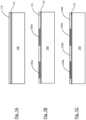
- Fig. 5 shows the layout of the structure obtained by the fabrication process of Figs. 1A - 1G and subsequent steps like those shown in figs. 4A - 4E .
- the device comprises a plurality of first thermoelectric elements 133a (n doped, e . g ., having a first Seebeck coefficient, particularly of a first sign, e . g ., positive) and a plurality of second thermoelectric elements 133b (p doped, e . g ., having a second, different Seebeck coefficient, particularly of an opposite sign, e . g ., negative).
- Each first thermoelectric element and each second thermoelectric element has a first end at the "hot” side of the device and a second end at the "cold” side of the device.
- the first and second thermoelectric elements 133a and 133b are arranged in alternated arrays that extend parallel to each other and are contacted (at the opposite ends of the thermoelectric elements, "hot” side and “cold” side") by the conductive lines 143 (here forming first conductive lines 257) and second conductive lines 413, in "zig-zag” fashion.
- the first conductive lines 257 have an input contact pad 257' and an output contact pad 257".
- thermoelectric elements 133a and 133b are thermally in parallel and electrically in series.
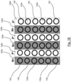
- Fig. 6 shows the layout of the structure obtained by the fabrication process of Figs. 2A - 2P (or 3A - 3L) and 4A - 4D and 4F.
- the device of Fig. 6 comprises a plurality of first thermoelectric elements 237 (n doped, e . g ., having a first Seebeck coefficient, particularly of a first sign, e.g., positive) and a plurality of second thermoelectric elements 249 (p doped, e.g., having a second, different Seebeck coefficient, particularly of an opposite sign, e . g ., negative).
- first thermoelectric element 237 and each second thermoelectric element 249 has a first end at the "hot" side of the device and a second end at the "cold" side of the device.
- the first and second thermoelectric elements 237 and 249 are arranged in alternated rows or arrays that extend parallelly to each other and are contacted (at the opposite ends of the thermoelectric elements, "hot” side and “cold” side") by the first conductive lines 257 and the second conductive lines 413, in "zig-zag” fashion.
- the second conductive lines 413 have an input contact pad 413' and an output contact pad 413".
- thermoelectric elements 237 and 249 are thermally in parallel and electrically in series.
- Fig. 7 schematically shows in terms of a simplified block diagram an electronic system 700 comprising a thermoelectric converter according to an embodiment of the present disclosure.
- the system 700 comprises a thermoelectric converter 705, for example a thermoelectric generator, adapted to convert heat, represented by the arrows 710, in an environment in which the system 700 is located, into electric energy which is exploited to charge a battery 715 of the system 700.
- the battery 715 supplies electric energy to an application 720, e.g., an electronic subsystem such as a smart watch, a wearable device, a torch, and so on.
- the proposed solution exhibits several advantages. It is easy to industrialize, provides power levels of the order of mA, has a low consumption of semiconductor area, and works with low or high temperature differences. Moreover, the proposed solution allows the size of standard thermoelectric devices to be reduced from macroscale to microscale and exploiting technological steps typical of semiconductor (Silicon) manufacturing technology.
- thermoelectric converter according to the present disclosure can be exploited in several practical applications, such as wearable and fitness gears, pedometers and heart-rate meters, smart watches and wrist bands, wireless sensor nodes for smart homes and cities, as well as in other energy harvesting systems, as discussed below with reference to Fig. 17 .
- thermoelectric converter according to the present disclosure may be used in solar energy recovery devices, as disclosed herein.
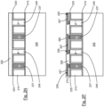
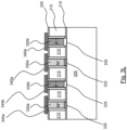
- Figs. 8 to 13 show some steps of a method according to an example embodiment of the present disclosure for manufacturing a solar energy recovery device using the thermoelectric converter of any one of the previously described embodiments.
- steps of the fabrication method which will be described hereafter apply as well to any of the embodiments described so far, for simplicity they will be described and shown as a continuation of the process steps described with reference to Figs. 4A to 4D and 4F.
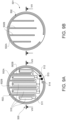
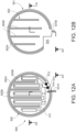
- Figs. 8 , 10 takenn along cross-section plane VIII-VIII of Figs. 9A, 9B
- Fig. 11 taken along cross-section plane XI-XI of Figs. 12A, 12B
- first conductive lines 257 are completely visible
- second conductive lines 413 are visible only in part.
- a third silicon wafer 501 is bonded to a surface 500A of the structure of Fig. 4F , here denoted by 500 and also called thermoelectric generator structure 500; surface 500A is opposite to the second silicon wafer 405.
- the third silicon wafer 501 may be a silicon wafer, in particular monocrystalline silicon, doped with acceptor dopants, thus of P type, and has a first surface 501A and a second surface 501B.
- the third silicon wafer 501 is bonded to thermoelectric generator structure 500 at its first surface 501A.
- bonding multilayer 502 may include a first bonding layer 504 extending on surface 500A of thermoelectric generator structure 500; a second bonding layer 505 extending on first surface 501A of the third silicon wafer 501; and an intermediate bonding layer 506.
- the material of the first bonding layer 504 and of the second bonding layer 505 may be copper (Cu); the material of intermediate bonding layer 506 may be tin (Sn).
- the first bonding layer 504, the second bonding layer 505 and the intermediate bonding layer 506 may be applied on either the surface 500A of thermoelectric generator structure 500 or on the first surface 501A of the third silicon wafer 501.
- the first bonding layer 504 may be applied to the surface 500A of thermoelectric generator structure 500
- the second bonding layer 505 may be applied to the first surface 501A of the third silicon wafer 501
- the intermediate bonding layer 506 may be applied on one of the latter.
- the bonding multilayer 502 is defined to form an annular portion 502A surrounding the area accommodating the thermoelectric elements 237, 249 in the thermoelectric generator structure 500 (see also Figs. 9A and 9B ).
- the bonding multilayer 502 further forms intermediate finger-like portions 502B that may be arranged in various ways in order to allow a good bonding and to allow connections to extend on surface 500A of thermoelectric generator structure 500 or on the first surface 501A of the third silicon wafer 501.
- thermoelectric elements 237, 249 of Fig. 8 form a plurality of thermoelectric modules 510 (see Fig. 9A ), coupled in parallel to each other.
- each thermoelectric module 510 may comprise one row thermoelectric elements 237 and one row of thermoelectric elements 249 (see, e.g., Fig. 6 ), coupled as also shown in Fig. 6 ; in the alternative, each thermoelectric module 510 may comprise the entire structure shown in e.g., Fig. 6 .
- thermoelectric modules 510 are coupled by connections 511 that may be formed partly in the oxide layer 270 and partly on the oxide layer 415 ( Fig. 8 ). Connections 511 are coupled to an input pad 512 and to an output pad 513 arranged on the periphery of the thermoelectric generator structure 500 in an interruption of the annular portion 502A of bonding multilayer 502. Input pad 512 and output pad 513 may be coupled to input contact pad 413' and to output contact pad 413" of fig. 6 by vias, in a per se known manner. In addition, the annular portion 502A forms a anode pad 514, as explained hereinafter.
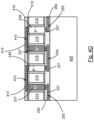
- an implant of N + -type doping species is performed in the third wafer 501 through the second surface 501B thereof.
- suitable N + -type doping species may be phosphorus or arsenic.
- the implant is annealed and activated by a powerful laser beam pulse.
- the pulse length may be in the order of a hundred nanosecond ( ⁇ 200 ns).
- cathode region 520 is formed.
- the heat generated by the pulse is enough for local annealing, eliminating local implantation damages and activating the dopants.
- no temperature change is produced in the metal regions; thereby, the bonding multilayer 502, the first and second conductive lines 257, 413 and the connections 511 are not affected.
- Cathode region 520 forms, together with the underlying portion of the third wafer 501 (also called hereinafter substrate 521, of P-type), a diode that is able to convert solar energy into a current, in a per se known manner.
- the third wafer 501 forms a solar photovoltaic cell wafer 201.
- the third wafer 501 is etched, to remove a portion thereof overlying pads 512-514 (see also Figs. 12A, 12B showing the thermoelectric generator structure 500 and the third wafer 501 as if there were not yet bonded). Etching may be performed by laser or blade cutting. Thereby, a recess 525 is formed that exposes pads 512-514.
- Wires 530 are bonded to the input and output pads 512, 513 and external connections 531A, 531B are bonded to the anode pad 514 and to the cathode region 520, respectively.
- the external connections 531A, 531B may be wires or cables.
- Fig. 13 shows an example connection of three solar photovoltaic-thermoelectric modules 550 to form a hybrid solar energy recovery device 570.
- a plurality of solar photovoltaic-thermoelectric modules 550 may be coupled to each other in series or in parallel, with the input pads 512 of all solar photovoltaic-thermoelectric modules 550 coupled together and the output pads 513 of all solar photovoltaic-thermoelectric modules 550 coupled together, through respective external connections 531A, 531B.
- Hybrid solar photovoltaic-thermoelectric device 570 is able to efficiently recover electric energy.
- waste heat produced at the solar photovoltaic cell wafer 501 may be recovered by the thermoelectric generator structure 500 and the total power is the sum of the power supplied by the thermoelectric generator 500 and the power supplied by the solar photovoltaic cell wafer 501, thereby providing a synergetic effect.
- Manufacturing may be made using usual techniques in the semiconductor industry. For example, the solar photovoltaic cell wafer 501 is bonded before front end. In this way, possible breakages (for example of metal regions) that may occur during bonding due to the pressure exerted by the piston on the two wafers are avoided.
- Figs. 14 and 15 show a thermoelectric generator, obtained by aerosol-jet printing of a semiconductor material. material which does not form part of the present invention.
- Maskless Mesoscale Material Deposition may be used for depositing the semiconductor material.
- bismuth telluride (Bi 2 Te 3 ) regions of opposite conductivity type are printed.
- Fig. 14 shows a first wafer 600 and a second wafer 601.
- First and second wafers 600, 601 may be silicon wafers, for example monocrystalline silicon wafers.
- One of the wafers 600, 601, here second wafer 601, is P-type.
- First wafer 600 has a surface 600A on which alternatively P-type bismuth telluride regions 604 and first adhesion regions 605 have been deposited using M3D.
- Second wafer 601 has a surface 601A on which alternatively N-type bismuth telluride regions 606 and second adhesion regions 607 have been deposited using M3D.
- P-type bismuth telluride regions 604 and first adhesion regions 605 are deposited on first metal regions 610 extending on the surface 600A of the first wafer 600.
- N-type bismuth telluride regions 606 and second adhesion regions 607 are deposited on second metal regions 611.
- First and second metal regions 610, 611 may be, for example, of gold (Au).
- a bismuth telluride region 604 or 606 and an adhesion region 605 or 607 are formed on each metal region 610 and the distance between a P-type bismuth telluride region 604 and the adjacent first adhesion regions 605 is the same as the distance between an N-type bismuth telluride region 606 and the adjacent second adhesion regions 607.
- metal regions 610, 611 typically have the pattern shown in Fig. 5 or 6 for the conductive lines 143 or 257 and 413 for connecting the bismuth telluride regions 604, 606 in series.
- Adhesion regions 605 and 607 may be a tin-silver (Sn-Ag) alloy and have a lower thickness than the bismuth telluride regions 604, 606.
- Bismuth telluride regions 604, 606 have here the same thickness, for example in the range 20-30 ⁇ m; adhesion regions 605, 607 have the same thickness, for example in the range 1-2 ⁇ m.
- First and second wafers 600, 601 are bonded to each other by turning one wafer (here second wafer 601) upside down and bonding the P-type bismuth telluride regions 604 to the second adhesion regions 607 and the N-type bismuth telluride regions 606 to the first adhesion regions 605, Fig. 15 .
- Bonding may be done by applying a pressure (e.g. 1-20 MPa) at a low temperature, e . g ., about 400°C.
- a pressure e.g. 1-20 MPa
- bismuth telluride regions 604, 606 form thermoelectric elements.
- an implant of N + -type doping species is performed in one of the wafers 600, 601, here second wafer 601, through its exposed surface.
- phosphorus or arsenic ions are implanted.
- the implant is annealed and activated by a powerful laser beam pulse, forming cathode region 620.
- the rest of the second wafer 601 forms an anode region 621.
- Fig. 15 may be subject to the manufacturing step discussed above with reference to Figs. 11 , 12A and 12B
- a plurality of solar photovoltaic-thermoelectric modules 650 may be coupled as shown in Fig. 13 , to form a hybrid solar energy recovery device.
- Fig. 16 shows a solar photovoltaic-thermoelectric module 750 that is similar to solar photovoltaic-thermoelectric module 650 of Fig. 15 but for the arrangement of the bismuth telluride regions 604, 606 that are here all formed on a same wafer, here the first wafer 600 and the adhesion regions, here denoted by reference number 705, that are all formed on the other wafer, here the second wafer 601.
- the other elements have been denoted by same reference numbers of Figs. 14-15 .
- both P-type and N-type bismuth telluride regions 604, 606 are printed on the first wafer 600 (after forming the first metal regions 610), and the adhesion regions 705 are printed all on the second wafer 601 (after forming the second metal regions 611).
- the solar photovoltaic-thermoelectric module 750 is obtained.
- the energy recovered by solar photovoltaic-thermoelectric module 650 of Fig. 15 or the solar photovoltaic-thermoelectric module 750 of Fig. 16 may be increased by the use of a passive cooling system, as shown in Fig. 17 .
- Fig. 17 shows a solar energy recovery system 800 comprising a solar collector panel 801 and a loop 802 for recirculating a cooling fluid.
- the cooling fluid is water and the following description is made considering water; other cooling fluids may however be used.
- the solar collector panel 801 accommodates a plurality of solar photovoltaic-thermoelectric modules 550, 650 or 750, coupled together as shown in Figure 13 .
- the solar photovoltaic-thermoelectric modules 550, 650 or 750 may be attached to a support wall 810 that delimits a water chamber 811 arranged along the loop 802.
- the water chamber 811 has an input (cold) side 811A and an output (warm) side 811B; the tank 803 is arranged near the output (warm) side 811B of the water chamber 811.
- the water in the loop 802 circulate without the need of pumps, due to the temperature gradient between the input (cold) side 811A and the output (warm) side 811B, as well as because of the principle of communication vessels.
- the loop 802 may include an underground section 820 that extends under the ground level (indicated by 830 in Fig. 17 ).
- underground section 820 by arranging underground section 820 at a depth of 8-10 m below the ground level 830, a particularly efficient extraction of heat from the cooling water is obtained, and no refrigeration machine or pump is needed.
- the loop 802 by recirculating the cooling water, provides a cooling of the solar collector panel 801 and thus a reduction in the temperature of the solar photovoltaic cell wafers 501, 601 as well as an increase in the photovoltaic effect.
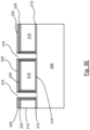
- Fig. 18 shows a possible embodiment of a solar photovoltaic cell wafer 900.
- Solar photovoltaic cell wafer 900 is based on the use of amorphous silicon, in case passivated by hydrogen (a-Si:H) and comprises a stack formed by a first doped layer 901, having an N-type conductivity; an intermediate, intrinsic layer 902, overlying the first doped layer 901; and a second doped layer 903, having a P-type conductivity, overlying the intermediate, intrinsic layer 902.
- a-Si:H passivated by hydrogen
- the structure of Fig. 18 may be obtained starting from the structure of Fig. 8 , by depositing, above the third wafer 501, an aluminum layer 905, the first doped layer 901, the intermediate, intrinsic layer 902, the second doped layer 903, a transparent conductive oxide (TCO) layer 906, and a glass layer 907.
- an aluminum layer 905 the first doped layer 901, the intermediate, intrinsic layer 902, the second doped layer 903, a transparent conductive oxide (TCO) layer 906, and a glass layer 907.
- TCO transparent conductive oxide
- the first doped layer 901 may have a thickness of about 10 nm; the intermediate, intrinsic layer 902 may have a thickness of about 400 nm; and the second doped layer 901 may have a thickness of about 10 nm.
- the TCO layer 906 may be, e.g., of indium-tin oxide.
- the intermediate, intrinsic layer 902 provides for an efficient absorption of light radiation, while the first and second doped layers 901, 903 provide an efficient generation of an electronic current, due to the fact that the electron-hole recombination is particularly high in doped silicon.
- the solar photovoltaic cell wafer 900 is thus very efficient and may advantageously combined with the thermoelectric generator structure described herein, for example with thermoelectric generator structure 500.
Landscapes
- Chemical & Material Sciences (AREA)
- Inorganic Chemistry (AREA)
- Engineering & Computer Science (AREA)
- Manufacturing & Machinery (AREA)
- Photovoltaic Devices (AREA)
- Semiconductor Integrated Circuits (AREA)
- Measuring Temperature Or Quantity Of Heat (AREA)
Description
- The present invention generally relates to the field of solid-state technology, particularly semiconductor technology and devices, and more particularly to a solid-state, integrated thermoelectric converter, like a ThermoElectric Generator (aka "TEG"), and to a fabrication method thereof.
- Direct conversion of thermal energy into electric energy (and vice-versa) by Seebeck effect is a promising approach for harvesting energy from heat sources, particularly when reduced temperature gradients are involved and that, as such, would otherwise not be exploited (such as waste heat of industrial plants, residual heat of car engines, low temperature thermal sources).
- Thermoelectric generators are low enthalpy waste heat exploitation devices that are used, for example, in battery-free radiator valve actuators or in torches (in this latter case, exploiting the difference in temperature between the human body temperature and the ambient temperature).
- Thermoelectric generators make use of thermoelectric materials that are capable of generating power directly from the heat by converting temperature differences into electric voltage.
- A good thermoelectric material should have both high electrical conductivity (σ) and low thermal conductivity (κ). Having low thermal conductivity ensures that when one side of the material is made hot, the other material side stays cold, which helps to generate a significant voltage even with a low temperature gradient.
- Tellurium-based thermoelectric generators make use, as thermoelectric material, of materials based on Tellurium.
- Tellurium compounds, such as Bismuth Telluride (Bi2Te3), exhibit good Seebeck coefficients (the Seebeck coefficient, also known as thermopower, thermoelectric power, thermoelectric sensitivity, of a material is a measure of the magnitude of an induced thermoelectric voltage in response to a temperature difference across that material, as induced by the Seebeck effect), high electrical conductivity and low thermal conductivity (just as an example, the thermal conductivity of Bismuth Telluride is 2W/mK). These properties make Bismuth Telluride suitable to be used to form the "thermoelectrically active elements" of a thermoelectric generator (by "thermoelectrically active elements" or "active elements" it is meant the thermoelectric elements in thermoelectric material that are capable of converting a thermal drop or temperature gradient across them into an electric potential by Seebeck effect).
- A Tellurium-based thermoelectric generator includes a plurality of interconnected n-doped Bismuth Telluride active elements and p-doped Bismuth Telluride active elements (the active elements being also referred to as "legs") between a pair of opposite ceramic substrates provided with metal (Cu or Au) contact regions and conductive lines, that interconnect the plurality of n-doped and p-doped Bismuth Telluride active elements. The n-doped Bismuth Telluride active elements are formed as discrete elements, typically by means of a process that involves forming ingots starting from powder material and then dicing the ingots to form pellets that will then form the Seebeck legs when the pellets are put (in a manual or semi-automatic assembling stage) between the two ceramic substrate.
- The existing Tellurium-based thermoelectric generators are therefore discrete components. Bismuth Telluride is not suitable to be used as a material in standard Integrated Circuit (IC) manufacturing processes, which instead are based on Silicon.
- Moreover, Tellurium-based thermoelectric generators typically exhibit a relatively good efficiency only in a limited temperature range (usually, of the order of 100 K around room temperature) and thermoelectric properties that rapidly degrade as temperature increases. This reduces the fields of application of the Tellurium-based thermoelectric generators.
- Additionally, Tellurium is a relatively rare element, which inherently limits a widespread use thereof.
- Furthermore, an extensive use of Tellurium compounds, such as Bismuth Telluride, could pose environmental problems, in particular in term of end-of-life device disposal.
- In silicon-based thermoelectric generators, materials based on Silicon (n-doped and p-doped, so as to exhibit different Seebeck coefficients) are used as thermoelectric material to form the active elements.
- Silicon-based thermoelectric generators manufactured with Silicon-compatible technologies can be classified in two families: in devices of a first family the heat flow is parallel to the substrate whereas in the other family the heat flow is orthogonal to the substrate ("out-of-plane" heat flux). The architectures of these integrated thermoelectric generators generally comprise a number of elementary cells having n-p doped legs, arranged in such a way that the elementary cells are thermally in parallel and electrically in series. Typically, integrated thermoelectric generators in which heat flows parallel to the substrate may have conductive legs of thermoelectrically active materials deposited over a very high thermal resistance material or a membrane, suspended several hundreds of micrometers above the substrate, or the legs of active materials themselves are free-standing (membrane-less).
- Out-of-plane heat flux thermoelectric generators minimizes thermal losses, simplify thermal coupling at system level, enhancing overall performance, and are amenable to miniaturization and integration in microelectronic and optoelectronic devices, among other applications.
- The paper by M. Tomita et al., "10µW/cm2-Class High Power Density Planar Si-Nanowire Thermoelectric Energy Harvester Compatible with CMOS-VLSI Technology", 38th IEEE Symposium on VLSI Technology, VLSI Technology 2018, Honolulu, United States, 18-22/6/18 criticizes planar Si-based thermoelectric generators employing long Si-nanowires about 10-100 µm as active elements, which are suspended on a cavity to cutoff the bypass of the heat current to secure the temperature difference across the Si-nanowires. The authors of the paper propose a design concept of planar and short thermoelectric generator without cavity structure, which uses a steep temperature gradient formed in the vicinity of the main heat current.
-
WO 2018/078515 discloses an integrated thermoelectric generator of out-of-plane heat flux configuration. The generator further includes a top capping layer deposited onto a free surface, oriented in an opposite direction in respect to said void spaces, of said planar electrically non-conductive cover layer so as to occlude the through holes of the non-conductive cover layer. - The article "Miniaturized thermoelectric generators based on poly-Si and poly-SiGe surface micromachining" by M. Strasser et al, SENSORS AND ACTUATORS A/PHYSICAL, ELSEVIER BY, NL, vol. 97-98, 1 April 2002, pages 535-542, XP004361648, ISSN: 0924-4247, DOI: 10.1016/S924-4247 (01) 00815-9 discloses generators using BiCMOS technology by forming thermocouples of opposite conductivity silicon in a thick poly-Si or poly Si-Ge layer that is patterned to form the n- and p- legs. LOCOS oxide is used to thermally isolate the cold and the hot side.
-
DE 10 2006 015492 discloses a thermoelectric generator comprising columnar elements of polysilicon and opposite conductivities extending from a substrate that are grown in separate steps. -
US 2006/102223 ,CN 106486593 andCN 103199188 disclose other thermoelectric generators of SiGe, or semiconductor alloys or metals. - The Applicant has realized that the Silicon-based thermoelectric generators proposed in the art exhibit drawbacks.
- Silicon has a large electrical conductivity and a good Seebeck coefficient, but, as a thermoelectric material, it has the disadvantage of featuring a high thermal conductivity (148 W/mK) compared to Bismuth Telluride (which has a thermal conductivity of 2 W/mK). Furthermore, Silicon-based thermoelectric generators having a cavity have a low mechanical stability because of the presence of the cavity. Other drawbacks of known Silicon-based thermoelectric generators are: difficulty to industrialize; low power (~ 100 µW /cm2); and high semiconductor area consumption.
- The Applicant has tackled, among others, the problem of devising a novel thermoelectric converter overcoming, among others, the drawbacks that affect known thermoelectric generators.
- According to the invention, a method of fabricating a thermoelectric converter and an integrated thermoelectric converter are provided, as defined in the attached claims.
- The features and advantages of the present disclosure will be made apparent by the following description of example embodiments thereof, provided merely as non-limitative examples.
- For its better intelligibility, the following description should be read making reference to the attached drawings, wherein:
-
Figs. 1A - 1G show some steps of a fabrication method of a thermoelectric converter according to the present disclosure; -
Figs. 2A - 2P show some steps of a fabrication method of a thermoelectric converter according to the present disclosure; -
Figs. 3A - 3L show some steps of a fabrication method of a thermoelectric converter according to still an example embodiment of the present disclosure; -
Figs. 4A - 4E show some steps of the fabrication method following the steps ofFigs. 2A - 2P orFigs. 3A - 3L , in an example embodiment of the present disclosure (same or similar process steps can also follow the steps ofFigs. 1A- 1G ); -
Fig. 4F shows example steps for the formation of contact pads; -
Fig. 5 shows, in top plan view, a layout of a thermoelectric converter obtained by a method according to an example embodiment of the present disclosure, including steps shown inFigs. 1A - 1G and steps similar to those ofFigs. 4A - 4E ; -
Fig. 6 show, in top plan view, a layout of a thermoelectric converter obtained by a method according to the embodiment of the present disclosure, including steps shown inFigs. 2A - 2P orFigs. 3A - 3L andFigs. 4A - 4E ; -
Fig. 7 shows a simplified block diagram of an electronic system comprising a thermoelectric converter according to an embodiment of the present disclosure; -
Figs. 8 shows a cross-section, taken along section line VIII-VIII ofFigs. 9A and 9B , of a solar energy recovery device using the thermoelectric converter ofFigure 4F , after bonding the thermoelectric wafer and a solar cell wafer; -
Fig. 9A is a top plan view of the thermoelectric wafer ofFigure 8 , before bonding; -
Fig. 9B is a bottom plan view of the solar cell wafer ofFigure 8 , before bonding; -
Figure 10 is a cross-section of the solar energy recovery device ofFig. 8 in a further manufacturing step; -
Figure 11 is a cross-section taken along section line XI-XI ofFigs. 12A and 12B of the solar energy recovery device ofFig. 10 in a further manufacturing step; -
Fig. 12A is a top plan view of the thermoelectric wafer ofFigure 11 ; -
Fig. 12B is a bottom plan view of the solar cell wafer ofFigure 11 ; -
Figure 13 is a scheme depicting a possible connection of the solar energy recovery device ofFig. 11 ; -
Figures 14 and15 show cross-sections of a solar energy recovery device not according to the present invention in different manufacturing steps; -
Figure 16 is a cross-section of a different solar energy recovery device not according to the present invention; -
Figure 17 is a schematic representation of a system disclosed therein; and -
Figure 18 is a cross-section of an example of a solar cell wafer that may be used in the solar energy recovery device according to this disclosure. - It is pointed out that the drawings in the figures are not necessarily drawn to scale.
- In the following, reference will be made to the drawings, which show some steps of fabrication methods of a thermoelectric converter according to example embodiments of the present disclosure. In the drawings, like and/or corresponding elements are denoted by like reference numerals.
- Reference is firstly made to
Figs. 1A - 1G , which show some steps of a fabrication method. - Starting from a Silicon substrate (first Silicon wafer) 105, a surface of the
Silicon substrate 105 is oxidized (e.g., by means of thermal oxidation) to form a layer ofoxide 110, e.g., Silicon dioxide (SiO2). Then, alayer 115 of polycrystalline SiGe is formed over the layer ofoxide 110. The resulting structure is schematically depicted inFig. 1A . - The
layer 115 of polycrystalline SiGe is for example a layer of polycrystalline Si0.7Ge0.3. Thelayer 115 of polycrystalline SiGe can for example be formed by means of deposition, for example, but not limitatively, chemical deposition, for example, Chemical Vapor Deposition (CVD); among the several different CVD techniques, Low Pressure CVD (LPCVD) can for example be exploited. Deposition takes place from silane (SiH4) and germane (GeH4). Alternatively, thelayer 115 of SiGe polysilicon can be formed by means of epitaxial growth in an epitaxial reactor. Both techniques produce aconformal layer 115 of polycrystalline SiGe. - The
layer 115 of polycrystalline SiGe can for example have a thickness of some microns, e.g., about 1 µm. - Then, as depicted in
Figs. 1B and 1C , alternated n+ dopedregions 120a and p+doped regions 120b of n+ doped and, respectively, p+ doped polycrystalline SiGe are formed in thelayer 115 of polycrystalline SiGe. The dopants (donor dopants for the n+ dopedregions 120a and acceptor dopants for the p+ dopedregions 120b) can be selectively introduced into thelayer 115 of polycrystalline SiGe by ion implantation. For example, suitable donor dopants can be Phosphorus or Arsenic, a suitable acceptor dopant can be Boron. The n+ dopedregions 120a and p+doped regions 120b can for example take shape of substantially parallel strips formed in thelayer 115 of polycrystalline SiGe (where "parallel" is meant to intend along a direction orthogonal to the plane of the drawing sheet ofFigs. 1B and 1C ), alternated and for example (but not limitatively) contiguous to each other (in a direction from the left to the right of the drawing sheet). - The steps of forming a layer of polycrystalline SiGe and forming, in the layer of polycrystalline SiGe, n+ and p+ doped regions are repeated twice or more times. As depicted in
Fig. 1D , every new layer of polycrystalline SiGe is formed (for example by the same technique as thefirst layer 115 of polycrystalline SiGe) on the preceding layer of polycrystalline SiGe, and in each newly formed layer of polycrystalline SiGe n+ and p+ dopedregions Fig. 1D ) alignment with the previously formed n+ and p+ dopedregions stacks 125a of n+ doped regions and thestacks 125b of p+ doped regions take the form of substantially parallel strips formed in the stack of layers of polycrystalline SiGe (where, again, "parallel" is meant to intend along the direction orthogonal to the plane of the drawing sheet ofFig. 1D ), alternated and for example (but not limitatively) contiguous to each other (in the direction from the left to the right of the drawing sheets), as visible, e.g., inFig. 1E . - The number of times that the steps of forming a layer of polycrystalline SiGe and forming, in the layer of polycrystalline SiGe, n+ and p+ doped regions are repeated depends on the thickness of each one of the layers of polycrystalline SiGe (the stacked layers of polycrystalline SiGe may have all the same thickness or different thicknesses from each other), and on the desired overall thickness of the stack of layers of polycrystalline SiGe. The overall thickness of the stack of layers of polycrystalline SiGe should be such as to ensure a sufficient thermal difference between the bottom and the top of the
stacks 125a of n+ doped regions and stacks 125b of p+ doped regions, even for relatively low temperature gradients. For example, the overall thickness of the stack of layers of polycrystalline SiGe can be of some tens of microns, particularly from about 10 µm to about 30 µm (thus, for an example thickness of the generic layer of polycrystalline SiGe of about 1 µm, the steps of forming a layer of polycrystalline SiGe and forming, in the layer of polycrystalline SiGe, n+ and p+ doped regions are repeated some tens of times). -
Trenches 130 are then formed in thestacks 125a of n+ doped regions and in thestacks 125b of p+ doped regions. Thetrenches 130 are for example formed as cylindrical shells. Thetrenches 130 extend down to the layer ofoxide 110.Multiple trenches 130 are formed along eachstack Fig. 1E . Eachtrench 130 delimits a respective (e.g., cylindrical)portion 133a of arespective stack 125a of n+ doped regions or a respective (e.g., cylindrical)portion 133b of arespective stack 125b of p+ doped regions, whichportions respective stack 125a of n+ doped regions and stack 125b of p+ doped regions. The (e.g., cylindrical)portions stacks 125a of n+ doped regions and of thestacks 125b of p+ doped regions will form the thermoelectrically active elements (e.g., the "legs") of the thermoelectric converter. - By means of an oxidation process the
trenches 130 are filled with oxide and the top surface of the structure (e.g., the surface opposite to the Silicon substrate 105) is covered by anoxide layer 135. The oxide can for example be SiO2. In particular, the oxidation process can involve a thermal oxidation process for coating the lateral walls of thetrenches 130 with oxide, followed by a deposition of a thick oxide layer using TEOS (TetraEthyl OrthoSilicate) filling the trenches and covering the surface of the structure with theoxide layer 135. The resulting structure is shown inFig. 1F . In this way, the (e.g., cylindrical) portions of thestacks 125a of n+ doped regions and of thestacks 125b of p+ doped regions which are delimited by thetrenches 130 remain insulated from the remaining of therespective stacks 125a of n+ doped regions and stacks 125b of p+ doped regions. As mentioned, the (e.g., cylindrical) portions of thestacks 125a of n+ doped regions and of thestacks 125b of p+ doped regions which are delimited by thetrenches 130 will form the thermoelectric elements (e.g., the "legs") 133a (n doped, e.g., having a first Seebeck coefficient, particularly of a first sign, e.g., positive) and 133b (p doped, e.g., having a second, different Seebeck coefficient, particularly of an opposite sign, e.g., negative) of the thermoelectric converter. - As visible in
Fig. 1G , contact openings are formed in theoxide layer 135 in correspondence of the n+ dopedthermoelectric elements 133a and of the p+ dopedthermoelectric elements 133b delimited by thetrenches 130, and aconductive layer 140, e.g., of a metal, is formed on theoxide layer 135 and then patterned to defineconductive lines 143 interconnecting the n+ dopedthermoelectric elements 133a and the p+ dopedthermoelectric elements 133b. The surface of the structure is then covered by alayer 145 of oxide, e.g., SiO2. - Reference is now made to
Figs. 2A - 2P , which show some steps of a method - Starting from a Silicon substrate (first Silicon wafer) 205, a surface of the
Silicon substrate 205 is oxidized to form a layer ofoxide 210, e.g., Silicon dioxide (SiO2). - Then, a (relatively thick)
layer 215 of polycrystalline Silicon ("epi-poly") is formed over the layer ofoxide 210. Thelayer 215 of polycrystalline Silicon is for example formed by means of epitaxial growth in an epitaxial reactor. - The resulting structure is depicted in
Fig. 2A . - The thickness J of the
layer 215 of polycrystalline Silicon should be such as to ensure a sufficient thermal difference between the bottom and the top of the thermoelectric elements that will be formed therewithin (as described in the following), even for relatively low ambient temperature gradients. For example, the thickness of thelayer 215 can be of some tens of microns, particularly from about 10 µm to about 30 µm. - A surface of the
layer 215 of polycrystalline Silicon is then oxidized to form alayer 220 of oxide, for example a layer of Silicon dioxide (SiO2). The resulting structure is shown inFig. 2B . - As shown in
Fig. 2C ,trenches 225 are then formed in thelayer 215 of polycrystalline Silicon. Thetrenches 225 extend down to the layer ofoxide 210 that covers the surface of theSilicon substrate 205. Thetrenches 225 may for example be cylindrical. Thetrenches 225 may for example have a width w of about 3 µm. - The walls of the
trenches 225 are then covered by a layer ofoxide 230, e.g., a layer of Silicon dioxide (SiO2), as depicted inFig. 2D , e.g., by means of thermal oxidation. In this way, cylindrical shells ofoxide 230 are created inside thetrenches 225. - A
layer 235 of n+ doped polycrystalline SiGe is formed over the surface of the structure (e.g., the surface opposite to the Silicon substrate 205). Thelayer 235 of n+ doped polycrystalline SiGe is for example a layer of n+ doped polycrystalline Si0.7Ge0.3 polysilicon. Thelayer 235 of n+ doped polycrystalline SiGe can for example be formed by means of deposition, particularly chemical deposition, even more particularly Chemical Vapor Deposition (CVD); among the several different CVD techniques, Low Pressure CVD (LPCVD) can be exploited. Deposition takes place from silane (SiH4) and germane (GeH4). The n+ doped polycrystalline SiGe is conformal. During the deposition process, n+ doped polycrystalline SiGe fills the trenches 225 (with walls covered by the oxide 230). The resulting structure is shown inFig. 2E . - By means of a Chemical-Mechanical Polishing ("CMP") step, the
layer 235 of n+ doped polycrystalline SiGe is removed from over the surface of thelayer 220 of oxide, leaving only (e.g., cylindrical)portions 237 of the n+ doped polycrystalline SiGe within the trenches 225 (with walls covered by the oxide 230), as depicted inFig. 2F . -
Further trenches 240 are then formed in thelayer 215. Like thetrenches 225, thefurther trenches 240 extend down to the layer ofoxide 210 covering the surface of theSilicon substrate 205. Thefurther trenches 240 may for example be cylindrical. Like thetrenches 225, thetrenches 240 may for example have a width of about 3 µm. Thefurther trenches 240 are formed so as to obtain a structure, shown inFig. 2G , in which thefurther trenches 240 are alternated with thetrenches 225. - The walls of the
further trenches 240 are then covered by a layer ofoxide 245, e.g., a layer of Silicon dioxide (SiO2), for example by means of a thermal oxidation process, as depicted inFig. 2H . In this way, cylindrical shells ofoxide 245 are created inside thetrenches 240. - A
layer 247 of p+ doped polycrystalline SiGe is formed over the surface of the structure. Thelayer 247 of p+ doped polycrystalline SiGe is for example a layer of p+ doped polycrystalline Si0.7Ge0.3. Thelayer 247 of p+ doped polycrystalline SiGe can for example be formed by means of deposition, particularly chemical deposition, even more particularly Chemical Vapor Deposition (CVD); among the several different CVD techniques, Low Pressure CVD (LPCVD) can be exploited. Deposition takes place from silane (SiH4) and germane (GeH4). The p+ doped polycrystalline SiGe is conformal. During the deposition process, p+ doped polycrystalline SiGe fills the further trenches 240 (with walls covered by the oxide 245). The resulting structure is shown inFig. 2L . - By means of a Chemical-Mechanical Polishing ("CMP") step, the
layer 247 of p+ doped polycrystalline SiGe is removed from over the surface of thelayer 220 of oxide, leaving only (e.g., cylindrical)portions 249 of the p+ doped polycrystalline SiGe within the further trenches 240 (with walls covered by the oxide 245), as depicted inFig. 2M . - In this way, the (e.g., cylindrical)
portions 237 of n+ doped polycrystalline SiGe and the (e.g., cylindrical)portions 249 of p+ doped polycrystalline SiGe which are delimited by thetrenches 225 and 245 (with walls covered by theoxide 230 and 245) remain insulated from the surroundinglayer 215 of polycrystalline Silicon. These (e.g., cylindrical)portions 237 of n+ doped polycrystalline SiGe andportions 249 of p+ doped polycrystalline SiGe will form the thermoelectric elements (e.g., the "legs") of the thermoelectric converter. - It is pointed out that each of the
portions 237 of n+ doped polycrystalline SiGe and each of theportions 249 of p+ doped polycrystalline SiGe which are visible inFig. 2M may identify a respective array ofportions 237 of n+ doped polycrystalline SiGe (each one formed inside arespective trench 225 with walls covered by the oxide 230) and a respective array ofportions 249 of n+ doped polycrystalline SiGe (each one formed inside a respectivefurther trench 240 with walls covered by the oxide 245), extending along a direction orthogonal to the plane of the drawing sheet ofFig. 2M (as can be clearly understood looking atFig. 5 , to be described later on). - The surface of the structure (opposite to the Silicon substrate 205) is then oxidized, to form a layer of
oxide 250, e.g., a layer of Silicon dioxide (SiO2), covering the whole surface of the structure, as shown inFig. 2N . - As visible in
Fig. 2P , contact openings are formed in theoxide layer 250 in correspondence of each of theportions 237 of n+ doped polycrystalline SiGe and each of theportions 249 of p+ doped polycrystalline SiGe, and aconductive layer 255, e.g., of a metal, is formed on theoxide layer 250 and then patterned to define firstconductive lines 257 interconnecting thethermoelectric elements further oxide layer 260, e.g., SiO2. Oxide layers 250 and 260 form, together asurface oxide layer 270 embedding the firstconductive lines 257. - According to the invention, the
thermoelectric elements thermoelectric elements -
Figs. 3A - 3L depicts some steps of a process for forming thethermoelectric elements - Starting from the structure shown in
Fig. 2B , a mask layer 305 (e.g., a Silicon nitride layer or a thick oxide layer) is formed over thelayer 220 of oxide, as depicted inFig. 3A . - As shown in
Fig. 3B ,trenches 310 are then formed by selective etching, whichtrenches 310, starting from the surface of the mask layer 305 (that protects the structure from etching where tranches are not to be formed), extend down to the layer ofoxide 210 that covers theSilicon substrate 205. Thetrenches 310 can be similar to thetrenches 225 of the previously described embodiment (for example, cylindrical trenches having a width of about 3 µm.). - As depicted in
Fig. 3C , the walls of thetrenches 310 are then coated by a layer ofoxide 315, for example by means of a thermal oxidation process. - As shown in
Fig. 3D , amask layer 320 of, e.g., Silicon nitride is then deposited over the whole structure. The material of themask layer 320 penetrates into thetrenches 310 and coats the walls and the bottom of thetrenches 310. - Moving to
Fig. 3E , the structure is subjected to an etch process during which part of themask layer 320 is etched away; the etch stops when the material of themask layer 320 and the portion of the layer ofoxide 210 at the bottom of thetrenches 310 are removed, thereby leaving theSilicon substrate 205 exposed at the bottom of thetrenches 310. - Process steps similar to those shown in
Figs. 2E - 2M are then performed to fill thetrenches 310 with n+ and p+ doped polycrystalline Silicon. - After a chemical-mechanical polishing step, the structure depicted in
Fig. 3F is obtained (in this and in the following figures the layer of Silicon nitride which, after the etch of step 3E, remains at the top surface and on the lateral walls of thetrenches 310, is not shown for the sake of better intelligibility). Thetrenches 310 are filled with (e.g., cylindrical)pillars - The
pillars pillars pillars Fig. 3G , wherereferences reference 335 denotes the bottom portions of thepillars - In embodiments, the process may envisage the formation (e.g., by deposition) of a layer of
polycrystalline Silicon 340 over the surface of the structure. Donor and acceptor dopant ions are then selectively implanted into thepolycrystalline Silicon 340 to form n+ and p+ dopedpolycrystalline Silicon areas porous Silicon Fig. 3H . The remaining portions of the layer of polycrystalline Silicon 340 (other than the n+ and p+ dopedpolycrystalline Silicon areas Fig. 3L . In this way, the n+ and p+ dopedpolycrystalline Silicon areas porous Silicon porous Silicon -
Figs. 4A to 4E show some steps of a method according to an example embodiment of the present disclosure for proceeding with the fabrication of the thermoelectric converter of any one of the previously described embodiments. Despite the steps of the fabrication method which will be described hereafter apply as well to any of the embodiments described so far, for mere reasons of simplicity they will be described and shown making reference to the second embodiment described inFigs. 2A-2P . - As shown in
Fig. 4A , starting from the structure offig. 2P , asecond Silicon wafer 405 is bonded to the surface of the structure opposite to the Silicon substrate (first Silicon wafer) 205. - The Silicon substrate (first Silicon wafer) 205 is then removed, as shown in
Fig. 4B (in which figure, as well as in the following figuresFig. 4C andFig. 4D , the structure is depicted upside-down compared toFig. 4A ). After removal of the Silicon substrate (first Silicon wafer) 205, thelayer 210 of oxide remains uncovered. - Contacts openings are formed in the
layer 210 of oxide in correspondence of thethermoelectric elements conductive layer 410, e.g., of a metal, is formed on theoxide layer 210 and then patterned to define secondconductive lines 413 interconnecting thethermoelectric elements Fig. 4C . - The surface of the structure is then covered by a
further layer 415 of oxide, e.g., SiO2, obtaining the structure ofFig. 4D . - The
second Silicon wafer 405 is then selectively etched to form trenches, leaving the material of the second Silicon wafer only over thethermoelectric elements second Silicon wafer 405 is removed, theoxide layer 260 that covered the firstconductive lines 257 is etched and removed to leaveportions 257', 257" of the firstconductive lines 257 exposed; the exposedportions 257', 257" of the firstconductive lines 257 will form contact pads of the thermoelectric converter, for soldering bonding wires 265 (similar portions of theconductive lines 143 in the structure ofFig. 1G will form the contact pads). The resulting structure is shown inFig. 4E (oriented similarly toFigs. 2A - 2P ). - The side of the structure where there is the (portion of the) second Silicon wafer 405 (left and not removed) will, in use, be for example the "hot" side of the thermoelectric converter (e.g., the side where the temperature of the environment where the thermoelectric converter is inserted is higher), while the opposite side of the structure will, in use, be for example the "cold" side of the thermoelectric converter (e.g., the side where the temperature of the environment where the thermoelectric converter is inserted is lower). Naturally, in use the role of the "hot" and "cold" sides of the thermoelectric converter can be reverted: generally, the two sides of the thermoelectric converter will in use experiment a temperature gradient. The portion(s) of the
second Silicon wafer 405 left and not removed can form a structural support for the device. -
Fig. 4F shows an alternative to steps 4D and 4E for the formation of contact pads for thebonding wires 265. In this case, the contact pads can be portions of the secondconductive lines 413 interconnecting thethermoelectric elements layer 415 of oxide is selectively etched. It is not necessary to selectively etch thesecond Silicon wafer 405, which can be left as it is for acting as a mechanical support for the structure. -
Fig. 5 shows the layout of the structure obtained by the fabrication process ofFigs. 1A - 1G and subsequent steps like those shown infigs. 4A - 4E . The device comprises a plurality of firstthermoelectric elements 133a (n doped, e.g., having a first Seebeck coefficient, particularly of a first sign, e.g., positive) and a plurality of secondthermoelectric elements 133b (p doped, e.g., having a second, different Seebeck coefficient, particularly of an opposite sign, e.g., negative). Each first thermoelectric element and each second thermoelectric element has a first end at the "hot" side of the device and a second end at the "cold" side of the device. The first and secondthermoelectric elements conductive lines 413, in "zig-zag" fashion. The firstconductive lines 257 have an input contact pad 257' and anoutput contact pad 257". - The first and second
thermoelectric elements -
Fig. 6 shows the layout of the structure obtained by the fabrication process ofFigs. 2A - 2P (or 3A - 3L) and 4A - 4D and 4F. - Therefore, the device of
Fig. 6 comprises a plurality of first thermoelectric elements 237 (n doped, e.g., having a first Seebeck coefficient, particularly of a first sign, e.g., positive) and a plurality of second thermoelectric elements 249 (p doped, e.g., having a second, different Seebeck coefficient, particularly of an opposite sign, e.g., negative). Each firstthermoelectric element 237 and each secondthermoelectric element 249 has a first end at the "hot" side of the device and a second end at the "cold" side of the device. The first and secondthermoelectric elements conductive lines 257 and the secondconductive lines 413, in "zig-zag" fashion. The secondconductive lines 413 have an input contact pad 413' and anoutput contact pad 413". - The first and second
thermoelectric elements -
Fig. 7 schematically shows in terms of a simplified block diagram anelectronic system 700 comprising a thermoelectric converter according to an embodiment of the present disclosure. - The
system 700 comprises athermoelectric converter 705, for example a thermoelectric generator, adapted to convert heat, represented by thearrows 710, in an environment in which thesystem 700 is located, into electric energy which is exploited to charge abattery 715 of thesystem 700. Thebattery 715 supplies electric energy to anapplication 720, e.g., an electronic subsystem such as a smart watch, a wearable device, a torch, and so on. - The proposed solution exhibits several advantages. It is easy to industrialize, provides power levels of the order of mA, has a low consumption of semiconductor area, and works with low or high temperature differences. Moreover, the proposed solution allows the size of standard thermoelectric devices to be reduced from macroscale to microscale and exploiting technological steps typical of semiconductor (Silicon) manufacturing technology.
- The thermoelectric converter according to the present disclosure can be exploited in several practical applications, such as wearable and fitness gears, pedometers and heart-rate meters, smart watches and wrist bands, wireless sensor nodes for smart homes and cities, as well as in other energy harvesting systems, as discussed below with reference to
Fig. 17 . - Furthermore, the thermoelectric converter according to the present disclosure may be used in solar energy recovery devices, as disclosed herein.
-
Figs. 8 to 13 show some steps of a method according to an example embodiment of the present disclosure for manufacturing a solar energy recovery device using the thermoelectric converter of any one of the previously described embodiments. Despite the steps of the fabrication method which will be described hereafter apply as well to any of the embodiments described so far, for simplicity they will be described and shown as a continuation of the process steps described with reference toFigs. 4A to 4D and 4F. In the cross-sections ofFigs. 8 ,10 (taken along cross-section plane VIII-VIII ofFigs. 9A, 9B ) and in the cross-section ofFig. 11 (taken along cross-section plane XI-XI ofFigs. 12A, 12B ), only the firstconductive lines 257 are completely visible; secondconductive lines 413 are visible only in part. - As shown in
Fig. 8 , athird silicon wafer 501 is bonded to a surface 500A of the structure ofFig. 4F , here denoted by 500 and also calledthermoelectric generator structure 500; surface 500A is opposite to thesecond silicon wafer 405. Thethird silicon wafer 501 may be a silicon wafer, in particular monocrystalline silicon, doped with acceptor dopants, thus of P type, and has afirst surface 501A and asecond surface 501B. Thethird silicon wafer 501 is bonded tothermoelectric generator structure 500 at itsfirst surface 501A. - To this end, a
bonding multilayer 502 is used; for example,bonding multilayer 502 may include afirst bonding layer 504 extending on surface 500A ofthermoelectric generator structure 500; asecond bonding layer 505 extending onfirst surface 501A of thethird silicon wafer 501; and anintermediate bonding layer 506. The material of thefirst bonding layer 504 and of thesecond bonding layer 505 may be copper (Cu); the material ofintermediate bonding layer 506 may be tin (Sn). - The
first bonding layer 504, thesecond bonding layer 505 and theintermediate bonding layer 506 may be applied on either the surface 500A ofthermoelectric generator structure 500 or on thefirst surface 501A of thethird silicon wafer 501. In the alternative, thefirst bonding layer 504 may be applied to the surface 500A ofthermoelectric generator structure 500, thesecond bonding layer 505 may be applied to thefirst surface 501A of thethird silicon wafer 501 and theintermediate bonding layer 506 may be applied on one of the latter. - In some embodiments, the
bonding multilayer 502 is defined to form anannular portion 502A surrounding the area accommodating thethermoelectric elements Figs. 9A and 9B ). Thebonding multilayer 502 further forms intermediate finger-like portions 502B that may be arranged in various ways in order to allow a good bonding and to allow connections to extend on surface 500A ofthermoelectric generator structure 500 or on thefirst surface 501A of thethird silicon wafer 501. - For example, the
thermoelectric elements Fig. 8 form a plurality of thermoelectric modules 510 (seeFig. 9A ), coupled in parallel to each other. In the embodiment ofFigs. 8 ,10 and11 , eachthermoelectric module 510 may comprise one rowthermoelectric elements 237 and one row of thermoelectric elements 249 (see, e.g.,Fig. 6 ), coupled as also shown inFig. 6 ; in the alternative, eachthermoelectric module 510 may comprise the entire structure shown in e.g.,Fig. 6 . - In some embodiments, the
thermoelectric modules 510 are coupled byconnections 511 that may be formed partly in theoxide layer 270 and partly on the oxide layer 415 (Fig. 8 ).Connections 511 are coupled to aninput pad 512 and to anoutput pad 513 arranged on the periphery of thethermoelectric generator structure 500 in an interruption of theannular portion 502A ofbonding multilayer 502.Input pad 512 andoutput pad 513 may be coupled to input contact pad 413' and tooutput contact pad 413" offig. 6 by vias, in a per se known manner. In addition, theannular portion 502A forms aanode pad 514, as explained hereinafter. - In
Fig. 10 , an implant of N+-type doping species is performed in thethird wafer 501 through thesecond surface 501B thereof. For example, suitable N+-type doping species may be phosphorus or arsenic. - Then, the implant is annealed and activated by a powerful laser beam pulse. The pulse length may be in the order of a hundred nanosecond (< 200 ns). Thereby,
cathode region 520 is formed. The heat generated by the pulse is enough for local annealing, eliminating local implantation damages and activating the dopants. In particular, using a very short pulse, no temperature change is produced in the metal regions; thereby, thebonding multilayer 502, the first and secondconductive lines connections 511 are not affected. -
Cathode region 520 forms, together with the underlying portion of the third wafer 501 (also called hereinaftersubstrate 521, of P-type), a diode that is able to convert solar energy into a current, in a per se known manner. Thereby, thethird wafer 501 forms a solar photovoltaic cell wafer 201. - In
Fig. 11 , thethird wafer 501 is etched, to remove a portion thereof overlying pads 512-514 (see alsoFigs. 12A, 12B showing thethermoelectric generator structure 500 and thethird wafer 501 as if there were not yet bonded). Etching may be performed by laser or blade cutting. Thereby, arecess 525 is formed that exposes pads 512-514. -
Wires 530 are bonded to the input andoutput pads external connections anode pad 514 and to thecathode region 520, respectively. Theexternal connections - Thereby, a solar photovoltaic-
thermoelectric module 550 is obtained. -
Fig. 13 shows an example connection of three solar photovoltaic-thermoelectric modules 550 to form a hybrid solarenergy recovery device 570. In general, a plurality of solar photovoltaic-thermoelectric modules 550 may be coupled to each other in series or in parallel, with theinput pads 512 of all solar photovoltaic-thermoelectric modules 550 coupled together and theoutput pads 513 of all solar photovoltaic-thermoelectric modules 550 coupled together, through respectiveexternal connections - Hybrid solar photovoltaic-
thermoelectric device 570 is able to efficiently recover electric energy. - Conventional solar cells are able to absorb photon energy of the solar radiation only at frequencies that are near the solar cell band-gap and the remaining energy is converted into thermal energy and wasted. In addition, the conversion efficiency drops with temperature.
- Vice versa, with the solar photovoltaic-thermoelectric modules of
Figs. 8-12 , waste heat produced at the solarphotovoltaic cell wafer 501 may be recovered by thethermoelectric generator structure 500 and the total power is the sum of the power supplied by thethermoelectric generator 500 and the power supplied by the solarphotovoltaic cell wafer 501, thereby providing a synergetic effect. - Manufacturing may be made using usual techniques in the semiconductor industry. For example, the solar
photovoltaic cell wafer 501 is bonded before front end. In this way, possible breakages (for example of metal regions) that may occur during bonding due to the pressure exerted by the piston on the two wafers are avoided. -
Figs. 14 and15 show a thermoelectric generator, obtained by aerosol-jet printing of a semiconductor material. material which does not form part of the present invention. In particular, Maskless Mesoscale Material Deposition (M3D) may be used for depositing the semiconductor material. According to one aspect bismuth telluride (Bi2Te3) regions of opposite conductivity type are printed. - For example,
Fig. 14 shows afirst wafer 600 and asecond wafer 601. First andsecond wafers wafers second wafer 601, is P-type. -
First wafer 600 has asurface 600A on which alternatively P-typebismuth telluride regions 604 andfirst adhesion regions 605 have been deposited using M3D. -
Second wafer 601 has asurface 601A on which alternatively N-typebismuth telluride regions 606 andsecond adhesion regions 607 have been deposited using M3D. - P-type
bismuth telluride regions 604 andfirst adhesion regions 605 are deposited onfirst metal regions 610 extending on thesurface 600A of thefirst wafer 600. N-typebismuth telluride regions 606 andsecond adhesion regions 607 are deposited onsecond metal regions 611. First andsecond metal regions - For example, a
bismuth telluride region adhesion region metal region 610 and the distance between a P-typebismuth telluride region 604 and the adjacentfirst adhesion regions 605 is the same as the distance between an N-typebismuth telluride region 606 and the adjacentsecond adhesion regions 607. - In addition, although completely visible in
Figs. 14-15 ,metal regions Fig. 5 or6 for theconductive lines bismuth telluride regions Adhesion regions bismuth telluride regions Bismuth telluride regions adhesion regions - First and
second wafers bismuth telluride regions 604 to thesecond adhesion regions 607 and the N-typebismuth telluride regions 606 to thefirst adhesion regions 605,Fig. 15 . - Bonding may be done by applying a pressure (e.g. 1-20 MPa) at a low temperature, e.g., about 400°C.
- After bonding,
bismuth telluride regions - Then, an implant of N+-type doping species is performed in one of the
wafers second wafer 601, through its exposed surface. For example, phosphorus or arsenic ions are implanted. - Then, the implant is annealed and activated by a powerful laser beam pulse, forming
cathode region 620. The rest of thesecond wafer 601 forms ananode region 621. - The structure of
Fig. 15 may be subject to the manufacturing step discussed above with reference toFigs. 11 ,12A and 12B - Thereby, a solar photovoltaic-
thermoelectric module 650 is obtained. - A plurality of solar photovoltaic-
thermoelectric modules 650 may be coupled as shown inFig. 13 , to form a hybrid solar energy recovery device. -
Fig. 16 shows a solar photovoltaic-thermoelectric module 750 that is similar to solar photovoltaic-thermoelectric module 650 ofFig. 15 but for the arrangement of thebismuth telluride regions first wafer 600 and the adhesion regions, here denoted byreference number 705, that are all formed on the other wafer, here the second wafer 601.The other elements have been denoted by same reference numbers ofFigs. 14-15 . - In some implementations, in the embodiment of
Fig. 16 , through a M3D printing technique, both P-type and N-typebismuth telluride regions adhesion regions 705 are printed all on the second wafer 601 (after forming the second metal regions 611). - After bonding the first and
second wafers thermoelectric module 750 is obtained. - The energy recovered by solar photovoltaic-
thermoelectric module 650 ofFig. 15 or the solar photovoltaic-thermoelectric module 750 ofFig. 16 may be increased by the use of a passive cooling system, as shown inFig. 17 . -
Fig. 17 shows a solarenergy recovery system 800 comprising asolar collector panel 801 and aloop 802 for recirculating a cooling fluid. In the considered system, the cooling fluid is water and the following description is made considering water; other cooling fluids may however be used. - A
tank 803, having a coldwater input tap 804 and a warmwater output tap 805, is arranged along thewater recirculation loop 802. - The
solar collector panel 801 accommodates a plurality of solar photovoltaic-thermoelectric modules Figure 13 . The solar photovoltaic-thermoelectric modules support wall 810 that delimits awater chamber 811 arranged along theloop 802. Thewater chamber 811 has an input (cold)side 811A and an output (warm)side 811B; thetank 803 is arranged near the output (warm)side 811B of thewater chamber 811. - The water in the
loop 802 circulate without the need of pumps, due to the temperature gradient between the input (cold)side 811A and the output (warm)side 811B, as well as because of the principle of communication vessels. - For example, the
loop 802 may include anunderground section 820 that extends under the ground level (indicated by 830 inFig. 17 ). In particular, by arrangingunderground section 820 at a depth of 8-10 m below theground level 830, a particularly efficient extraction of heat from the cooling water is obtained, and no refrigeration machine or pump is needed. - The
loop 802, by recirculating the cooling water, provides a cooling of thesolar collector panel 801 and thus a reduction in the temperature of the solarphotovoltaic cell wafers -
Fig. 18 shows a possible embodiment of a solarphotovoltaic cell wafer 900. - Solar
photovoltaic cell wafer 900 is based on the use of amorphous silicon, in case passivated by hydrogen (a-Si:H) and comprises a stack formed by a first dopedlayer 901, having an N-type conductivity; an intermediate,intrinsic layer 902, overlying the first dopedlayer 901; and a second dopedlayer 903, having a P-type conductivity, overlying the intermediate,intrinsic layer 902. - For example, the structure of
Fig. 18 may be obtained starting from the structure ofFig. 8 , by depositing, above thethird wafer 501, analuminum layer 905, the first dopedlayer 901, the intermediate,intrinsic layer 902, the second dopedlayer 903, a transparent conductive oxide (TCO)layer 906, and aglass layer 907. - In an embodiment, the first doped
layer 901 may have a thickness of about 10 nm; the intermediate,intrinsic layer 902 may have a thickness of about 400 nm; and the second dopedlayer 901 may have a thickness of about 10 nm. - The
TCO layer 906 may be, e.g., of indium-tin oxide. - The intermediate,
intrinsic layer 902 provides for an efficient absorption of light radiation, while the first and seconddoped layers photovoltaic cell wafer 900 is thus very efficient and may advantageously combined with the thermoelectric generator structure described herein, for example withthermoelectric generator structure 500.
Claims (13)
- A method of fabricating a thermoelectric converter, comprising:forming a plurality of first thermoelectrically active elements (133a; 237; 330a) of a first thermoelectric semiconductor material having a first Seebeck coefficient and a plurality of second thermoelectrically active elements (133b; 249; 330b) of a second thermoelectric semiconductor material having a second Seebeck coefficient in a layer (115; 215) of silicon-based material, the layer of the silicon-based material having a first surface, a second surface opposite to the first surface, and a first thickness between the first surface and the second surface, the first and second thermoelectrically active elements each being formed to extend through the first thickness, from the first surface to the second surface; andforming electrically conductive interconnections (143, 413; 257, 413) over at least one of the first surface or the second surface of the layer of the silicon-based material (115; 215), the electrically conductive interconnections each electrically interconnecting a first thermoelectrically active element of the plurality of first thermoelectrically active elements and a corresponding one of the plurality of second thermoelectrically active elements; and forming an input electrical terminal and an output electrical terminal electrically coupled to the electrically conductive interconnections,wherein the first thermoelectric semiconductor material includes porous silicon and the second thermoelectric semiconductor material includes a silicon-based material selected from a group consisting of porous silicon and polycrystalline silicon.
- The method of claim 1, wherein the layer (115; 215) of the silicon-based material is a material selected among polycrystalline SiGe having a material composition of Si0.7Ge0.3, or epitaxial polycrystalline silicon.
- The method of claim 1 or 2, wherein the plurality of first thermoelectrically active elements (133a; 237; 330a) of the first thermoelectric semiconductor material having a first Seebeck coefficient are doped with acceptor dopants, and the plurality of second thermoelectrically active elements (133b; 249; 330b) of the second thermoelectric semiconductor material having a second Seebeck coefficient are doped with donor dopants.
- The method of any one of the preceding claims, wherein the layer of the silicon-based material is polycrystalline silicon, and the method comprises growing epitaxially the layer (115; 215) of polycrystalline silicon on an oxidized surface of a substrate.
- The method of claim 4, wherein the forming the plurality of first thermoelectrically active elements (237) of the first thermoelectric semiconductor material having the first Seebeck coefficient comprises:forming first trenches (225, 230) in the layer of the silicon-based material, andfilling the first trenches with polycrystalline silicon doped with acceptor dopants; andwherein the forming the plurality of second thermoelectrically active elements of the second thermoelectric semiconductor material having the second Seebeck coefficient comprises:forming second trenches (240, 245) in the layer (215) of the silicon-based material, andfilling the second trenches with polycrystalline silicon doped with donor dopants andconverting the doped polycrystalline silicon filling the first and second trenches into doped porous silicon.
- The method of the preceding claim, wherein converting the doped polycrystalline silicon comprises forming anisotropic porous silicon.
- The method of any one of the preceding claims, further comprising:
bonding the layer of silicon-based material to a wafer (501) intended to form solar photovoltaic cells. - The method of the preceding claim, wherein bonding the layer of silicon-based material comprises forming a conductive bonding layer (513) in electrical contact with the wafer (501) and forming a first electrical contact for wafer (501).
- The method of the preceding claim, wherein the wafer (501) comprises a first region (521) of a first conductivity type, the method including implanting doping species to form a second region (520) of a second conductivity type, opposite to the first conductivity type, and forming a second electrical contact (531) electrically coupled to the second region.
- An integrated thermoelectric converter, comprising:a first column structure (133a; 237; 330a), the first column structure including porous silicon doped with a first conductivity type;a second column structure (133b; 249; 330b), the second column structure including one of porous silicon, or polycrystalline silicon and doped with a second conductivity type; anda first electrically conductive interconnection structure (143, 413; 257, 413; 257') in electrical contact with a first end of the first column structure and a first end of the second column structure.
- The integrated thermoelectric converter of the preceding claim, comprising a first insulation structure (230) surrounding the first column structure (237) and a second insulation structure (230) surrounding the second column structure (249).
- The integrated thermoelectric converter of the preceding claim, wherein the first and second column structures include anisotropic silicon.
- The integrated thermoelectric converter of claim 10, comprising a substrate, wherein the first column structure includes a first portion of porous silicon and a second portion of polycrystalline silicon, the second portion between the first portion and the substrate.
Applications Claiming Priority (2)
| Application Number | Priority Date | Filing Date | Title |
|---|---|---|---|
| IT202000011335 | 2020-05-18 | ||
| US17/321,252 US11696504B2 (en) | 2020-05-18 | 2021-05-14 | Method of fabrication of an integrated thermoelectric converter, and integrated thermoelectric converter thus obtained |
Publications (3)
| Publication Number | Publication Date |
|---|---|
| EP3913681A2 EP3913681A2 (en) | 2021-11-24 |
| EP3913681A3 EP3913681A3 (en) | 2022-03-16 |
| EP3913681B1 true EP3913681B1 (en) | 2024-09-18 |
Family
ID=75870564
Family Applications (1)
| Application Number | Title | Priority Date | Filing Date |
|---|---|---|---|
| EP21174210.1A Active EP3913681B1 (en) | 2020-05-18 | 2021-05-17 | Method of fabrication of an integrated thermoelectric converter, and integrated thermoelectric converter thus obtained |
Country Status (3)
| Country | Link |
|---|---|
| US (1) | US20230301191A1 (en) |
| EP (1) | EP3913681B1 (en) |
| CN (1) | CN215496783U (en) |
Families Citing this family (12)
| Publication number | Priority date | Publication date | Assignee | Title |
|---|---|---|---|---|
| US11282815B2 (en) | 2020-01-14 | 2022-03-22 | Micron Technology, Inc. | Methods of forming microelectronic devices, and related microelectronic devices and electronic systems |
| US11696504B2 (en) * | 2020-05-18 | 2023-07-04 | Stmicroelectronics S.R.L. | Method of fabrication of an integrated thermoelectric converter, and integrated thermoelectric converter thus obtained |
| US11563018B2 (en) | 2020-06-18 | 2023-01-24 | Micron Technology, Inc. | Microelectronic devices, and related methods, memory devices, and electronic systems |
| US11380669B2 (en) * | 2020-06-18 | 2022-07-05 | Micron Technology, Inc. | Methods of forming microelectronic devices |
| US11705367B2 (en) | 2020-06-18 | 2023-07-18 | Micron Technology, Inc. | Methods of forming microelectronic devices, and related microelectronic devices, memory devices, electronic systems, and additional methods |
| US11699652B2 (en) | 2020-06-18 | 2023-07-11 | Micron Technology, Inc. | Microelectronic devices and electronic systems |
| US11557569B2 (en) | 2020-06-18 | 2023-01-17 | Micron Technology, Inc. | Microelectronic devices including source structures overlying stack structures, and related electronic systems |
| US11417676B2 (en) | 2020-08-24 | 2022-08-16 | Micron Technology, Inc. | Methods of forming microelectronic devices and memory devices, and related microelectronic devices, memory devices, and electronic systems |
| US11825658B2 (en) | 2020-08-24 | 2023-11-21 | Micron Technology, Inc. | Methods of forming microelectronic devices and memory devices |
| US11751408B2 (en) | 2021-02-02 | 2023-09-05 | Micron Technology, Inc. | Methods of forming microelectronic devices, and related microelectronic devices, memory devices, and electronic systems |
| IT202100024386A1 (en) * | 2021-09-22 | 2023-03-22 | St Microelectronics Srl | INTEGRATED THERMAL SENSOR AND RELATED MANUFACTURING PROCESS |
| PL444240A1 (en) * | 2023-03-29 | 2024-09-30 | Akademia Górniczo-Hutnicza im. Stanisława Staszica w Krakowie | Thermoelectric converter made of functionally graded materials |
Family Cites Families (11)
| Publication number | Priority date | Publication date | Assignee | Title |
|---|---|---|---|---|
| US7544883B2 (en) * | 2004-11-12 | 2009-06-09 | International Business Machines Corporation | Integrated thermoelectric cooling devices and methods for fabricating same |
| DE102006015492A1 (en) * | 2006-04-03 | 2007-10-04 | Robert Bosch Gmbh | Micromechanical element e.g. thermo-generator, has thermobranches provided with epitaxial polysilicon materials, where one thermobranch has electrical isolation material opposite to other thermobranch in direction of main extending level |
| FR2925225B1 (en) * | 2007-12-17 | 2010-06-11 | Commissariat Energie Atomique | ENERGY GENERATING DEVICE COMPRISING A PHOTOVOLTAIC CONVERTER AND A THERMOELECTRIC CONVERTER, THE SAME INCLUDING WITHIN THE PHOTOVOLTAIC CONVERTER SUPPORT SUBSTRATE |
| US20110048488A1 (en) * | 2009-09-01 | 2011-03-03 | Gabriel Karim M | Combined thermoelectric/photovoltaic device and method of making the same |
| US20110174362A1 (en) * | 2010-01-18 | 2011-07-21 | Applied Materials, Inc. | Manufacture of thin film solar cells with high conversion efficiency |
| CN103199188B (en) * | 2012-01-09 | 2016-06-08 | 天津大学 | The miniature thermoelectric device of laminated construction manufactured by thin-film thermoelectric material and manufacture method |
| CN102856278B (en) * | 2012-09-17 | 2015-08-05 | 华进半导体封装先导技术研发中心有限公司 | Adapter plate structure and manufacture method thereof |
| JP6232703B2 (en) * | 2013-01-11 | 2017-11-22 | 富士通株式会社 | Thermoelectric conversion element |
| KR20140110811A (en) * | 2014-07-22 | 2014-09-17 | 홍익대학교 산학협력단 | Fabrication methods of thermoelectric thin film modules using adhesive flip chip bonding and thermoelectric thin film modules produced using the same method |
| CN106486593B (en) * | 2015-08-26 | 2018-09-28 | 中国科学院上海微系统与信息技术研究所 | Minisize thermoelectric energy collecting device of bilateral pore structure and preparation method thereof |
| IT201600109345A1 (en) | 2016-10-28 | 2018-04-28 | Consorzio Delta Ti Res | Integrated thermoelectric generator and relative manufacturing method |
-
2021
- 2021-05-17 EP EP21174210.1A patent/EP3913681B1/en active Active
- 2021-05-18 CN CN202121062528.3U patent/CN215496783U/en active Active
-
2023
- 2023-05-24 US US18/323,262 patent/US20230301191A1/en active Pending
Also Published As
| Publication number | Publication date |
|---|---|
| US20230301191A1 (en) | 2023-09-21 |
| EP3913681A3 (en) | 2022-03-16 |
| CN215496783U (en) | 2022-01-11 |
| EP3913681A2 (en) | 2021-11-24 |
Similar Documents
| Publication | Publication Date | Title |
|---|---|---|
| EP3913681B1 (en) | Method of fabrication of an integrated thermoelectric converter, and integrated thermoelectric converter thus obtained | |
| KR101889429B1 (en) | Bypass Diode for a Solar Cell | |
| JP6328606B2 (en) | Semiconductor wafer cell and module processing for back contact photovoltaic modules | |
| JP5459957B2 (en) | Method for contact separation of conductive layer on back contact solar cell and solar cell | |
| Yan et al. | MEMS-based thermoelectric–photoelectric integrated power generator | |
| US20110083711A1 (en) | Energy generating device comprising a photovoltaic converter and a thermoelectric converter, the latter converter being included within the supporting substrate of the photovoltaic converter | |
| US20150179846A1 (en) | Structures and fabrication methods for solar cells and modules | |
| TW201027773A (en) | Back contact solar cell modules | |
| KR20060035657A (en) | Emitter wrap-through back contact solar cells on thin silicon wafers | |
| US11696504B2 (en) | Method of fabrication of an integrated thermoelectric converter, and integrated thermoelectric converter thus obtained | |
| KR101020475B1 (en) | Solar cell-thermoelectric integrated module and manufacturing method thereof | |
| EP3204967B1 (en) | 3d integrated thermoelectric generator operating in an out-of-plane heat flux configuration with internal voids and heat conduction paths conditioning vias | |
| EP3198648A1 (en) | Silicon integrated, out-of-plane heat flux thermoelectric generator | |
| KR20160112150A (en) | Phtovoltaic-Thermoelectric hybrid generator and method for fabricating the same | |
| EP3533085B1 (en) | Integrated thermoelectric generator and related method of fabrication | |
| US11362252B2 (en) | Thin film thermoelectric generator | |
| EP2056362A2 (en) | Multi-junction multi-spectral solar converter | |
| KR20210020461A (en) | Nanowire Thermoelectric device having a 3-Dimensional Stacked Nanowire and Method of Manufacturing the same | |
| WO2015130989A1 (en) | Self aligned contacts for back contact solar cells | |
| CN108511591A (en) | Polysilicon nanowire rectangular array and superlattices photoconductive structure miniature energy collector | |
| JP2005260158A (en) | Solar cell module | |
| Asscher et al. | Local isolation of high-voltage photovoltaic cells using buried layers of oxidized porous silicon | |
| EP4284148B1 (en) | Mems thermoelectric generator, manufacturing process of the generator and heating system comprising the generator | |
| Iulianella et al. | Integrated Thermoelectric Generator and related Method of Fabrication | |
| CA2643540A1 (en) | Multi-junction multi-spectral solar converter |
Legal Events
| Date | Code | Title | Description |
|---|---|---|---|
| PUAI | Public reference made under article 153(3) epc to a published international application that has entered the european phase |
Free format text: ORIGINAL CODE: 0009012 |
|
| STAA | Information on the status of an ep patent application or granted ep patent |
Free format text: STATUS: THE APPLICATION HAS BEEN PUBLISHED |
|
| AK | Designated contracting states |
Kind code of ref document: A2 Designated state(s): AL AT BE BG CH CY CZ DE DK EE ES FI FR GB GR HR HU IE IS IT LI LT LU LV MC MK MT NL NO PL PT RO RS SE SI SK SM TR |
|
| PUAL | Search report despatched |
Free format text: ORIGINAL CODE: 0009013 |
|
| RIC1 | Information provided on ipc code assigned before grant |
Ipc: H01L 31/052 20140101ALI20220114BHEP Ipc: H01L 35/34 20060101ALI20220114BHEP Ipc: H01L 35/22 20060101ALI20220114BHEP Ipc: H01L 27/16 20060101AFI20220114BHEP |
|
| AK | Designated contracting states |
Kind code of ref document: A3 Designated state(s): AL AT BE BG CH CY CZ DE DK EE ES FI FR GB GR HR HU IE IS IT LI LT LU LV MC MK MT NL NO PL PT RO RS SE SI SK SM TR |
|
| RIC1 | Information provided on ipc code assigned before grant |
Ipc: H01L 31/052 20140101ALI20220208BHEP Ipc: H01L 35/34 20060101ALI20220208BHEP Ipc: H01L 35/22 20060101ALI20220208BHEP Ipc: H01L 27/16 20060101AFI20220208BHEP |
|
| STAA | Information on the status of an ep patent application or granted ep patent |
Free format text: STATUS: REQUEST FOR EXAMINATION WAS MADE |
|
| 17P | Request for examination filed |
Effective date: 20220915 |
|
| RBV | Designated contracting states (corrected) |
Designated state(s): AL AT BE BG CH CY CZ DE DK EE ES FI FR GB GR HR HU IE IS IT LI LT LU LV MC MK MT NL NO PL PT RO RS SE SI SK SM TR |
|
| REG | Reference to a national code |
Ref country code: DE Ref legal event code: R079 Free format text: PREVIOUS MAIN CLASS: H01L0027160000 Ipc: H01L0031052000 Ref document number: 602021018856 Country of ref document: DE |
|
| RIC1 | Information provided on ipc code assigned before grant |
Ipc: H10N 10/852 20230101ALI20240216BHEP Ipc: H10N 10/17 20230101ALI20240216BHEP Ipc: H10N 10/851 20230101ALI20240216BHEP Ipc: H10N 10/01 20230101ALI20240216BHEP Ipc: H10N 19/00 20230101ALI20240216BHEP Ipc: H01L 31/052 20140101AFI20240216BHEP |
|
| GRAP | Despatch of communication of intention to grant a patent |
Free format text: ORIGINAL CODE: EPIDOSNIGR1 |
|
| STAA | Information on the status of an ep patent application or granted ep patent |
Free format text: STATUS: GRANT OF PATENT IS INTENDED |
|
| INTG | Intention to grant announced |
Effective date: 20240410 |
|
| RIN1 | Information on inventor provided before grant (corrected) |
Inventor name: MURARI, BRUNO Inventor name: SCOLARI, MARTINA Inventor name: ZANOTTI, LUCA Inventor name: SEGHIZZI, LUCA Inventor name: NOMELLINI, ANDREA Inventor name: ZULLINO, LUCIA Inventor name: VILLA, FLAVIO FRANCESCO Inventor name: FERRARI, PAOLO |
|
| GRAS | Grant fee paid |
Free format text: ORIGINAL CODE: EPIDOSNIGR3 |
|
| GRAA | (expected) grant |
Free format text: ORIGINAL CODE: 0009210 |
|
| STAA | Information on the status of an ep patent application or granted ep patent |
Free format text: STATUS: THE PATENT HAS BEEN GRANTED |
|
| AK | Designated contracting states |
Kind code of ref document: B1 Designated state(s): AL AT BE BG CH CY CZ DE DK EE ES FI FR GB GR HR HU IE IS IT LI LT LU LV MC MK MT NL NO PL PT RO RS SE SI SK SM TR |
|
| REG | Reference to a national code |
Ref country code: GB Ref legal event code: FG4D |
|
| REG | Reference to a national code |
Ref country code: CH Ref legal event code: EP |
|
| REG | Reference to a national code |
Ref country code: IE Ref legal event code: FG4D |
|
| REG | Reference to a national code |
Ref country code: DE Ref legal event code: R096 Ref document number: 602021018856 Country of ref document: DE |
|
| REG | Reference to a national code |
Ref country code: DE Ref legal event code: R079 Ref document number: 602021018856 Country of ref document: DE Free format text: PREVIOUS MAIN CLASS: H01L0031052000 Ipc: H10F0077630000 |
|
| REG | Reference to a national code |
Ref country code: LT Ref legal event code: MG9D |
|
| PG25 | Lapsed in a contracting state [announced via postgrant information from national office to epo] |
Ref country code: NO Free format text: LAPSE BECAUSE OF FAILURE TO SUBMIT A TRANSLATION OF THE DESCRIPTION OR TO PAY THE FEE WITHIN THE PRESCRIBED TIME-LIMIT Effective date: 20241218 |
|
| PG25 | Lapsed in a contracting state [announced via postgrant information from national office to epo] |
Ref country code: GR Free format text: LAPSE BECAUSE OF FAILURE TO SUBMIT A TRANSLATION OF THE DESCRIPTION OR TO PAY THE FEE WITHIN THE PRESCRIBED TIME-LIMIT Effective date: 20241219 Ref country code: FI Free format text: LAPSE BECAUSE OF FAILURE TO SUBMIT A TRANSLATION OF THE DESCRIPTION OR TO PAY THE FEE WITHIN THE PRESCRIBED TIME-LIMIT Effective date: 20240918 |
|
| PG25 | Lapsed in a contracting state [announced via postgrant information from national office to epo] |
Ref country code: BG Free format text: LAPSE BECAUSE OF FAILURE TO SUBMIT A TRANSLATION OF THE DESCRIPTION OR TO PAY THE FEE WITHIN THE PRESCRIBED TIME-LIMIT Effective date: 20240918 |
|
| PG25 | Lapsed in a contracting state [announced via postgrant information from national office to epo] |
Ref country code: LV Free format text: LAPSE BECAUSE OF FAILURE TO SUBMIT A TRANSLATION OF THE DESCRIPTION OR TO PAY THE FEE WITHIN THE PRESCRIBED TIME-LIMIT Effective date: 20240918 |
|
| PG25 | Lapsed in a contracting state [announced via postgrant information from national office to epo] |
Ref country code: HR Free format text: LAPSE BECAUSE OF FAILURE TO SUBMIT A TRANSLATION OF THE DESCRIPTION OR TO PAY THE FEE WITHIN THE PRESCRIBED TIME-LIMIT Effective date: 20240918 |
|
| REG | Reference to a national code |
Ref country code: NL Ref legal event code: MP Effective date: 20240918 |
|
| PG25 | Lapsed in a contracting state [announced via postgrant information from national office to epo] |
Ref country code: RS Free format text: LAPSE BECAUSE OF FAILURE TO SUBMIT A TRANSLATION OF THE DESCRIPTION OR TO PAY THE FEE WITHIN THE PRESCRIBED TIME-LIMIT Effective date: 20241218 |
|
| PG25 | Lapsed in a contracting state [announced via postgrant information from national office to epo] |
Ref country code: RS Free format text: LAPSE BECAUSE OF FAILURE TO SUBMIT A TRANSLATION OF THE DESCRIPTION OR TO PAY THE FEE WITHIN THE PRESCRIBED TIME-LIMIT Effective date: 20241218 Ref country code: NO Free format text: LAPSE BECAUSE OF FAILURE TO SUBMIT A TRANSLATION OF THE DESCRIPTION OR TO PAY THE FEE WITHIN THE PRESCRIBED TIME-LIMIT Effective date: 20241218 Ref country code: LV Free format text: LAPSE BECAUSE OF FAILURE TO SUBMIT A TRANSLATION OF THE DESCRIPTION OR TO PAY THE FEE WITHIN THE PRESCRIBED TIME-LIMIT Effective date: 20240918 Ref country code: HR Free format text: LAPSE BECAUSE OF FAILURE TO SUBMIT A TRANSLATION OF THE DESCRIPTION OR TO PAY THE FEE WITHIN THE PRESCRIBED TIME-LIMIT Effective date: 20240918 Ref country code: GR Free format text: LAPSE BECAUSE OF FAILURE TO SUBMIT A TRANSLATION OF THE DESCRIPTION OR TO PAY THE FEE WITHIN THE PRESCRIBED TIME-LIMIT Effective date: 20241219 Ref country code: FI Free format text: LAPSE BECAUSE OF FAILURE TO SUBMIT A TRANSLATION OF THE DESCRIPTION OR TO PAY THE FEE WITHIN THE PRESCRIBED TIME-LIMIT Effective date: 20240918 Ref country code: BG Free format text: LAPSE BECAUSE OF FAILURE TO SUBMIT A TRANSLATION OF THE DESCRIPTION OR TO PAY THE FEE WITHIN THE PRESCRIBED TIME-LIMIT Effective date: 20240918 |
|
| REG | Reference to a national code |
Ref country code: AT Ref legal event code: MK05 Ref document number: 1725449 Country of ref document: AT Kind code of ref document: T Effective date: 20240918 |
|
| PG25 | Lapsed in a contracting state [announced via postgrant information from national office to epo] |
Ref country code: NL Free format text: LAPSE BECAUSE OF FAILURE TO SUBMIT A TRANSLATION OF THE DESCRIPTION OR TO PAY THE FEE WITHIN THE PRESCRIBED TIME-LIMIT Effective date: 20240918 |
|
| PG25 | Lapsed in a contracting state [announced via postgrant information from national office to epo] |
Ref country code: IS Free format text: LAPSE BECAUSE OF FAILURE TO SUBMIT A TRANSLATION OF THE DESCRIPTION OR TO PAY THE FEE WITHIN THE PRESCRIBED TIME-LIMIT Effective date: 20250118 Ref country code: PT Free format text: LAPSE BECAUSE OF FAILURE TO SUBMIT A TRANSLATION OF THE DESCRIPTION OR TO PAY THE FEE WITHIN THE PRESCRIBED TIME-LIMIT Effective date: 20250120 |
|
| PG25 | Lapsed in a contracting state [announced via postgrant information from national office to epo] |
Ref country code: RO Free format text: LAPSE BECAUSE OF FAILURE TO SUBMIT A TRANSLATION OF THE DESCRIPTION OR TO PAY THE FEE WITHIN THE PRESCRIBED TIME-LIMIT Effective date: 20240918 Ref country code: SM Free format text: LAPSE BECAUSE OF FAILURE TO SUBMIT A TRANSLATION OF THE DESCRIPTION OR TO PAY THE FEE WITHIN THE PRESCRIBED TIME-LIMIT Effective date: 20240918 |
|
| PG25 | Lapsed in a contracting state [announced via postgrant information from national office to epo] |
Ref country code: ES Free format text: LAPSE BECAUSE OF FAILURE TO SUBMIT A TRANSLATION OF THE DESCRIPTION OR TO PAY THE FEE WITHIN THE PRESCRIBED TIME-LIMIT Effective date: 20240918 |
|
| PG25 | Lapsed in a contracting state [announced via postgrant information from national office to epo] |
Ref country code: EE Free format text: LAPSE BECAUSE OF FAILURE TO SUBMIT A TRANSLATION OF THE DESCRIPTION OR TO PAY THE FEE WITHIN THE PRESCRIBED TIME-LIMIT Effective date: 20240918 Ref country code: AT Free format text: LAPSE BECAUSE OF FAILURE TO SUBMIT A TRANSLATION OF THE DESCRIPTION OR TO PAY THE FEE WITHIN THE PRESCRIBED TIME-LIMIT Effective date: 20240918 |
|
| PG25 | Lapsed in a contracting state [announced via postgrant information from national office to epo] |
Ref country code: CZ Free format text: LAPSE BECAUSE OF FAILURE TO SUBMIT A TRANSLATION OF THE DESCRIPTION OR TO PAY THE FEE WITHIN THE PRESCRIBED TIME-LIMIT Effective date: 20240918 Ref country code: PL Free format text: LAPSE BECAUSE OF FAILURE TO SUBMIT A TRANSLATION OF THE DESCRIPTION OR TO PAY THE FEE WITHIN THE PRESCRIBED TIME-LIMIT Effective date: 20240918 |
|
| PG25 | Lapsed in a contracting state [announced via postgrant information from national office to epo] |
Ref country code: IT Free format text: LAPSE BECAUSE OF FAILURE TO SUBMIT A TRANSLATION OF THE DESCRIPTION OR TO PAY THE FEE WITHIN THE PRESCRIBED TIME-LIMIT Effective date: 20240918 Ref country code: SK Free format text: LAPSE BECAUSE OF FAILURE TO SUBMIT A TRANSLATION OF THE DESCRIPTION OR TO PAY THE FEE WITHIN THE PRESCRIBED TIME-LIMIT Effective date: 20240918 |
|
| REG | Reference to a national code |
Ref country code: DE Ref legal event code: R097 Ref document number: 602021018856 Country of ref document: DE |
|
| PGFP | Annual fee paid to national office [announced via postgrant information from national office to epo] |
Ref country code: DE Payment date: 20250423 Year of fee payment: 5 |
|
| PG25 | Lapsed in a contracting state [announced via postgrant information from national office to epo] |
Ref country code: DK Free format text: LAPSE BECAUSE OF FAILURE TO SUBMIT A TRANSLATION OF THE DESCRIPTION OR TO PAY THE FEE WITHIN THE PRESCRIBED TIME-LIMIT Effective date: 20240918 |
|
| PLBE | No opposition filed within time limit |
Free format text: ORIGINAL CODE: 0009261 |
|
| STAA | Information on the status of an ep patent application or granted ep patent |
Free format text: STATUS: NO OPPOSITION FILED WITHIN TIME LIMIT |
|
| 26N | No opposition filed |
Effective date: 20250619 |
|
| PG25 | Lapsed in a contracting state [announced via postgrant information from national office to epo] |
Ref country code: SE Free format text: LAPSE BECAUSE OF FAILURE TO SUBMIT A TRANSLATION OF THE DESCRIPTION OR TO PAY THE FEE WITHIN THE PRESCRIBED TIME-LIMIT Effective date: 20240918 |
|
| REG | Reference to a national code |
Ref country code: CH Ref legal event code: H13 Free format text: ST27 STATUS EVENT CODE: U-0-0-H10-H13 (AS PROVIDED BY THE NATIONAL OFFICE) Effective date: 20251223 |
|
| PG25 | Lapsed in a contracting state [announced via postgrant information from national office to epo] |
Ref country code: LU Free format text: LAPSE BECAUSE OF NON-PAYMENT OF DUE FEES Effective date: 20250517 |
|
| PG25 | Lapsed in a contracting state [announced via postgrant information from national office to epo] |
Ref country code: CH Free format text: LAPSE BECAUSE OF NON-PAYMENT OF DUE FEES Effective date: 20250531 |
|
| GBPC | Gb: european patent ceased through non-payment of renewal fee |
Effective date: 20250517 |
|
| REG | Reference to a national code |
Ref country code: BE Ref legal event code: MM Effective date: 20250531 |
|
| PG25 | Lapsed in a contracting state [announced via postgrant information from national office to epo] |
Ref country code: MC Free format text: LAPSE BECAUSE OF FAILURE TO SUBMIT A TRANSLATION OF THE DESCRIPTION OR TO PAY THE FEE WITHIN THE PRESCRIBED TIME-LIMIT Effective date: 20240918 |
|
| PG25 | Lapsed in a contracting state [announced via postgrant information from national office to epo] |
Ref country code: GB Free format text: LAPSE BECAUSE OF NON-PAYMENT OF DUE FEES Effective date: 20250517 |
|
| PG25 | Lapsed in a contracting state [announced via postgrant information from national office to epo] |
Ref country code: IE Free format text: LAPSE BECAUSE OF NON-PAYMENT OF DUE FEES Effective date: 20250517 |
|
| PG25 | Lapsed in a contracting state [announced via postgrant information from national office to epo] |
Ref country code: BE Free format text: LAPSE BECAUSE OF NON-PAYMENT OF DUE FEES Effective date: 20250531 |
|
| PG25 | Lapsed in a contracting state [announced via postgrant information from national office to epo] |
Ref country code: FR Free format text: LAPSE BECAUSE OF NON-PAYMENT OF DUE FEES Effective date: 20250531 |