EP3913632A1 - Method for testing memory and related equipment - Google Patents
Method for testing memory and related equipment Download PDFInfo
- Publication number
- EP3913632A1 EP3913632A1 EP20918133.8A EP20918133A EP3913632A1 EP 3913632 A1 EP3913632 A1 EP 3913632A1 EP 20918133 A EP20918133 A EP 20918133A EP 3913632 A1 EP3913632 A1 EP 3913632A1
- Authority
- EP
- European Patent Office
- Prior art keywords
- tested
- memory
- test
- address
- clock signal
- Prior art date
- Legal status (The legal status is an assumption and is not a legal conclusion. Google has not performed a legal analysis and makes no representation as to the accuracy of the status listed.)
- Granted
Links
Images





Classifications
-
- G—PHYSICS
- G11—INFORMATION STORAGE
- G11C—STATIC STORES
- G11C29/00—Checking stores for correct operation ; Subsequent repair; Testing stores during standby or offline operation
- G11C29/04—Detection or location of defective memory elements, e.g. cell constructio details, timing of test signals
- G11C29/08—Functional testing, e.g. testing during refresh, power-on self testing [POST] or distributed testing
- G11C29/12—Built-in arrangements for testing, e.g. built-in self testing [BIST] or interconnection details
-
- G—PHYSICS
- G11—INFORMATION STORAGE
- G11C—STATIC STORES
- G11C29/00—Checking stores for correct operation ; Subsequent repair; Testing stores during standby or offline operation
- G11C29/04—Detection or location of defective memory elements, e.g. cell constructio details, timing of test signals
- G11C29/08—Functional testing, e.g. testing during refresh, power-on self testing [POST] or distributed testing
- G11C29/48—Arrangements in static stores specially adapted for testing by means external to the store, e.g. using direct memory access [DMA] or using auxiliary access paths
-
- G—PHYSICS
- G11—INFORMATION STORAGE
- G11C—STATIC STORES
- G11C29/00—Checking stores for correct operation ; Subsequent repair; Testing stores during standby or offline operation
- G11C29/56—External testing equipment for static stores, e.g. automatic test equipment [ATE]; Interfaces therefor
- G11C29/56008—Error analysis, representation of errors
-
- G—PHYSICS
- G11—INFORMATION STORAGE
- G11C—STATIC STORES
- G11C29/00—Checking stores for correct operation ; Subsequent repair; Testing stores during standby or offline operation
- G11C29/04—Detection or location of defective memory elements, e.g. cell constructio details, timing of test signals
- G11C29/08—Functional testing, e.g. testing during refresh, power-on self testing [POST] or distributed testing
- G11C29/12—Built-in arrangements for testing, e.g. built-in self testing [BIST] or interconnection details
- G11C29/1201—Built-in arrangements for testing, e.g. built-in self testing [BIST] or interconnection details comprising I/O circuitry
-
- G—PHYSICS
- G11—INFORMATION STORAGE
- G11C—STATIC STORES
- G11C29/00—Checking stores for correct operation ; Subsequent repair; Testing stores during standby or offline operation
- G11C29/04—Detection or location of defective memory elements, e.g. cell constructio details, timing of test signals
- G11C29/08—Functional testing, e.g. testing during refresh, power-on self testing [POST] or distributed testing
- G11C29/12—Built-in arrangements for testing, e.g. built-in self testing [BIST] or interconnection details
- G11C29/12015—Built-in arrangements for testing, e.g. built-in self testing [BIST] or interconnection details comprising clock generation or timing circuitry
-
- G—PHYSICS
- G11—INFORMATION STORAGE
- G11C—STATIC STORES
- G11C29/00—Checking stores for correct operation ; Subsequent repair; Testing stores during standby or offline operation
- G11C29/04—Detection or location of defective memory elements, e.g. cell constructio details, timing of test signals
- G11C29/08—Functional testing, e.g. testing during refresh, power-on self testing [POST] or distributed testing
- G11C29/12—Built-in arrangements for testing, e.g. built-in self testing [BIST] or interconnection details
- G11C29/14—Implementation of control logic, e.g. test mode decoders
-
- G—PHYSICS
- G11—INFORMATION STORAGE
- G11C—STATIC STORES
- G11C29/00—Checking stores for correct operation ; Subsequent repair; Testing stores during standby or offline operation
- G11C29/04—Detection or location of defective memory elements, e.g. cell constructio details, timing of test signals
- G11C29/08—Functional testing, e.g. testing during refresh, power-on self testing [POST] or distributed testing
- G11C29/12—Built-in arrangements for testing, e.g. built-in self testing [BIST] or interconnection details
- G11C29/18—Address generation devices; Devices for accessing memories, e.g. details of addressing circuits
-
- G—PHYSICS
- G11—INFORMATION STORAGE
- G11C—STATIC STORES
- G11C29/00—Checking stores for correct operation ; Subsequent repair; Testing stores during standby or offline operation
- G11C29/04—Detection or location of defective memory elements, e.g. cell constructio details, timing of test signals
- G11C29/08—Functional testing, e.g. testing during refresh, power-on self testing [POST] or distributed testing
- G11C29/12—Built-in arrangements for testing, e.g. built-in self testing [BIST] or interconnection details
- G11C29/44—Indication or identification of errors, e.g. for repair
- G11C29/4401—Indication or identification of errors, e.g. for repair for self repair
-
- G—PHYSICS
- G11—INFORMATION STORAGE
- G11C—STATIC STORES
- G11C29/00—Checking stores for correct operation ; Subsequent repair; Testing stores during standby or offline operation
- G11C29/04—Detection or location of defective memory elements, e.g. cell constructio details, timing of test signals
- G11C29/08—Functional testing, e.g. testing during refresh, power-on self testing [POST] or distributed testing
- G11C29/12—Built-in arrangements for testing, e.g. built-in self testing [BIST] or interconnection details
- G11C29/46—Test trigger logic
-
- G—PHYSICS
- G11—INFORMATION STORAGE
- G11C—STATIC STORES
- G11C29/00—Checking stores for correct operation ; Subsequent repair; Testing stores during standby or offline operation
- G11C29/56—External testing equipment for static stores, e.g. automatic test equipment [ATE]; Interfaces therefor
- G11C29/56004—Pattern generation
-
- G—PHYSICS
- G11—INFORMATION STORAGE
- G11C—STATIC STORES
- G11C29/00—Checking stores for correct operation ; Subsequent repair; Testing stores during standby or offline operation
- G11C29/56—External testing equipment for static stores, e.g. automatic test equipment [ATE]; Interfaces therefor
- G11C29/56012—Timing aspects, clock generation, synchronisation
-
- G—PHYSICS
- G11—INFORMATION STORAGE
- G11C—STATIC STORES
- G11C29/00—Checking stores for correct operation ; Subsequent repair; Testing stores during standby or offline operation
- G11C29/04—Detection or location of defective memory elements, e.g. cell constructio details, timing of test signals
- G11C29/08—Functional testing, e.g. testing during refresh, power-on self testing [POST] or distributed testing
- G11C29/12—Built-in arrangements for testing, e.g. built-in self testing [BIST] or interconnection details
- G11C2029/1206—Location of test circuitry on chip or wafer
-
- G—PHYSICS
- G11—INFORMATION STORAGE
- G11C—STATIC STORES
- G11C29/00—Checking stores for correct operation ; Subsequent repair; Testing stores during standby or offline operation
- G11C29/04—Detection or location of defective memory elements, e.g. cell constructio details, timing of test signals
- G11C29/08—Functional testing, e.g. testing during refresh, power-on self testing [POST] or distributed testing
- G11C29/12—Built-in arrangements for testing, e.g. built-in self testing [BIST] or interconnection details
- G11C2029/1208—Error catch memory
-
- G—PHYSICS
- G11—INFORMATION STORAGE
- G11C—STATIC STORES
- G11C29/00—Checking stores for correct operation ; Subsequent repair; Testing stores during standby or offline operation
- G11C29/04—Detection or location of defective memory elements, e.g. cell constructio details, timing of test signals
- G11C29/08—Functional testing, e.g. testing during refresh, power-on self testing [POST] or distributed testing
- G11C29/12—Built-in arrangements for testing, e.g. built-in self testing [BIST] or interconnection details
- G11C29/38—Response verification devices
- G11C29/40—Response verification devices using compression techniques
- G11C2029/4002—Comparison of products, i.e. test results of chips or with golden chip
-
- G—PHYSICS
- G11—INFORMATION STORAGE
- G11C—STATIC STORES
- G11C29/00—Checking stores for correct operation ; Subsequent repair; Testing stores during standby or offline operation
- G11C29/04—Detection or location of defective memory elements, e.g. cell constructio details, timing of test signals
- G11C29/08—Functional testing, e.g. testing during refresh, power-on self testing [POST] or distributed testing
- G11C29/12—Built-in arrangements for testing, e.g. built-in self testing [BIST] or interconnection details
- G11C2029/4402—Internal storage of test result, quality data, chip identification, repair information
-
- G—PHYSICS
- G11—INFORMATION STORAGE
- G11C—STATIC STORES
- G11C29/00—Checking stores for correct operation ; Subsequent repair; Testing stores during standby or offline operation
- G11C29/56—External testing equipment for static stores, e.g. automatic test equipment [ATE]; Interfaces therefor
- G11C2029/5602—Interface to device under test
-
- G—PHYSICS
- G11—INFORMATION STORAGE
- G11C—STATIC STORES
- G11C29/00—Checking stores for correct operation ; Subsequent repair; Testing stores during standby or offline operation
- G11C29/006—Checking stores for correct operation ; Subsequent repair; Testing stores during standby or offline operation at wafer scale level, i.e. wafer scale integration [WSI]
-
- G—PHYSICS
- G11—INFORMATION STORAGE
- G11C—STATIC STORES
- G11C29/00—Checking stores for correct operation ; Subsequent repair; Testing stores during standby or offline operation
- G11C29/70—Masking faults in memories by using spares or by reconfiguring
- G11C29/78—Masking faults in memories by using spares or by reconfiguring using programmable devices
- G11C29/835—Masking faults in memories by using spares or by reconfiguring using programmable devices with roll call arrangements for redundant substitutions
Definitions
- the disclosure relates to the technical field of semiconductor testing, and more particularly, to a method and a related device for testing a memory.
- RAM Random-Access Memory
- ATE Automatic Test Equipment
- DRAM Dynamic Random Access Memory
- DA Pads Direct Access Pads
- the disclosure provides a method and a related device for testing a memory to overcome technical problems of the high test cost, the long test cycle, and limited test speed caused by the use of ATE to test the memory in the aforementioned related technologies.
- One aspect of the disclosure is directed to a method for testing a memory.
- the method includes: obtaining a test instruction; generating, in response to the test instruction, a test clock signal, a to-be-tested address and to-be-tested data; determining a to-be-tested memory from memories of a storage device, the storage device comprising a self-test circuit; writing the to-be-tested data into a storage unit corresponding to a to-be-tested address of the to-be-tested memory; reading output data from the storage unit corresponding to the to-be-tested address of the to-be-tested memory; and comparing the to-be-tested data with the output data corresponding to the to-be-tested address, to obtain a test result of the to-be-tested memory.
- the self-test circuit may include a first-in-first-out queue.
- the step of obtaining the test instruction may include: buffering a command signal from an automatic test equipment in the first-in-first-out queue, where a operating frequency of the test clock signal is higher than a frequency of a clock signal output by the automatic test equipment, or, a frequency of the test clock signal is equal to the frequency of the clock signal output by the automatic test equipment, and a phase of the test clock signal is different from a phase of the clock signal output by the automatic test equipment; and reading the command signal from the first-in-first-out queue.
- the step of obtaining the test instruction may further include determining a target operating mode of the self-test circuit; and parsing the command signal based on the target operating mode and determining the command signal to be the test instruction.
- the step of determining a target operating mode of the self-test circuit may include obtaining, from the automatic test equipment, first configuration information; and determining, based on the first configuration information, the target operating mode.
- the self-test circuit may further include a clock signal generator.
- the method may further include: obtaining, from the automatic test equipment, second configuration information; determining, based on the second configuration information, the frequency of the test clock signal; and generating, by using the clock signal generator, a test clock signal that has the frequency of the clock signal generator.
- the step of reading the command signal from the first-in-first-out queue may include: obtaining, from the automatic test equipment, third configuration information; determining, based on the third configuration information, a reading frequency of the command signal; and, in response to the reading frequency being equal to the frequency of the test clock signal, reading, based on the test clock signal, the command signal from the first-in-first-out queue.
- the step of reading the command signal from the first-in-first-out queue may further include: in response to the reading frequency being equal to the frequency of the clock signal output by the automatic test equipment, reading, based on the clock signal output by the automatic test equipment, the command signal from the first-in-first-out queue.
- the step of determining the to-be-tested memory from the memories of the storage device may include: obtaining, from the automatic test equipment, fourth configuration information; and determining, based on the fourth configuration information, the to-be-tested memory, the to-be-tested memory being one or more target memories in the storage device.
- the step of writing the to-be-tested data into the storage unit corresponding to the to-be-tested address of the to-be-tested memory may include: in response to the to-be-tested memory being one target memory in the storage device, writing the to-be-tested data into a storage unit corresponding to a to-be-tested address of the target memory.
- the step of writing the to-be-tested data into the storage unit corresponding to the to-be-tested address of the to-be-tested memory may include: in response to the to-be-tested memory being a plurality of target memories in the storage device, writing each of the to-be-tested data into storage units corresponding to a to-be-tested address of a respective one of the plurality of target memories.
- the step of comparing the to-be-tested data with the output data corresponding to the to-be-tested address, to obtain the test result of the to-be-tested memory may include: comparing the to-be-tested data with the output data corresponding to the to-be-tested address, to obtain a comparison result; and in response to the comparison result being not matching, recording the to-be-tested address corresponding to the to-be-tested data as an incorrect address, the test result including the incorrect address.
- the self-test circuit may include a volatile storage unit and a non-volatile storage unit.
- the method may further include writing the test result of the to-be-tested memory into the volatile storage unit; and writing the test result in the volatile storage unit into the non-volatile storage unit for storage.
- the self-test circuit may include a non-volatile storage unit, configured to store an incorrect address of the to-be-tested memory.
- the step of generating, in response to the test instruction, the to-be-tested address may include obtaining the incorrect address stored in the non-volatile storage unit; and skipping automatically the incorrect address when generating the to-be-tested address.
- the storage device may further include a control die.
- the self-test circuit may be arranged in the control die.
- the memories of the storage device may be vertically stacked above or beneath the control die.
- the self-test circuit may be arranged in the memories of the storage device.
- the method may be performed by the self-test circuit.
- the device may include a test instruction obtaining unit, an address data generation unit, a to-be-tested memory determination unit, a to-be-tested data writing unit, an output data reading unit, and a test result obtaining unit.
- the test instruction obtaining unit is configured to obtain a test instruction.
- the address data generation unit is configured to generate, in response to the test instruction, a test clock signal, a to-be-tested address and to-be-tested data.
- the to-be-tested memory determination unit is configured to determine a to-be-tested memory from memories of a storage device.
- the storage device includes a self-test circuit.
- the to-be-tested data writing unit is configured to write the to-be-tested data into a storage unit corresponding to a to-be-tested address of the to-be-tested memory.
- the output data reading unit is configured to read output data from the storage unit corresponding to the to-be-tested address of the to-be-tested memory.
- the test result obtaining unit is configured to compare the to-be-tested data with the output data corresponding to the to-be-tested address, to obtain a test result of the to-be-tested memory.
- the electronic device may include one or more processors and a storage device.
- the storage device may be configured to store one or more programs.
- the one or more programs may cause the one or more processors to perform any one of the foregoing methods for testing the memory.
- the storage medium may store a computer program. Upon being executed by a processor, the computer program may cause any one of the foregoing methods for testing the memory to be performed.
- a self-test circuit is added to complete a memory test, so that the test for a whole wafer may be completed by using a small quantity of DA pads in one touch down.
- the self-test circuit may be configured to generate a high-speed clock for the memory test, so that a low-speed ATE can be configured to complete a high-speed memory test, thereby reducing the test time and the test cost.
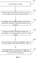
- FIG. 2 is a schematic flowchart of a method for testing a memory according to an embodiment of the disclosure. As shown in FIG. 2 , the method provided in this embodiment of the disclosure includes the following steps of S210 to S260.
- the method may be performed by a self-test circuit.
- the self-test circuit may be an internal circuit with a test capability in a storage device, and therefore may also be referred to as a built-in self-test (BIST) circuit.
- BIST built-in self-test
- the BIST circuit may be disposed in a control die of a storage device corresponding to a to-be-tested memory, or may be disposed in a memory die such as a DRAM die in the storage device. This is not limited in the disclosure.
- step of S210 a test instruction is obtained.
- the self-test circuit may include a First-In-First-Out (FIFO) queue.
- FIFO First-In-First-Out
- the step of obtaining the test instruction may include buffering a command signal from an automatic test equipment (ATE) in the FIFO queue.
- An operating frequency of the test clock signal may be higher than a frequency of a clock signal output by the ATE.
- a frequency of the test clock signal may be equal to the frequency of the clock signal output by the ATE, and a phase of the test clock signal may be different from a phase of the clock signal output by the ATE.
- the test instruction may be obtained by reading the command signal from the FIFO queue.
- the data sent by the ATE to the BIST circuit can be buffered in the built-in FIFO queue in the BIST circuit.
- the problem of frequency mismatch between a low-speed clock of the ATE and a high-speed clock of the BIST circuit may be resolved, thereby preventing the data sent by the ATE to the BIST circuit from being lost.
- phase inconsistency between the ATE and the BIST circuit may also cause the data loss.
- the data in of the BIST circuit to avoid frequent bus operations and reduce the burden on the central processing unit.
- the step of reading the command signal from the FIFO queue may include: obtaining third configuration information from the ATE; determining a reading frequency of the command signal based on the third configuration information; and in response to the reading frequency being equal to the frequency of the test clock signal, reading the command signal from the FIFO queue based on the test clock signal.
- the step of reading the command signal from the FIFO queue may further include: in response to the reading frequency being equal to the frequency of the clock signal output by the ATE, reading the command signal from the FIFO queue based on the clock signal output by the ATE.
- the ATE may send the third configuration information to the BIST circuit to specify the frequency of reading the buffered command signal from the FIFO queue in the BIST circuit. It may be specified that the buffered command signal is read from the FIFO queue in the BIST circuit based on a high-speed clock generated by the BIST circuit or based on a low-speed clock of the ATE. This is not limited in the disclosure.
- the step of obtaining the test instruction may further include: determining a target operating mode of the self-test circuit; and parsing the command signal based on the target operating mode and determining the command signal to be the test instruction.
- the step of determining the target operating mode of the self-test circuit may include: obtaining first configuration information from the ATE; and determining the target operating mode based on the first configuration information.
- the various command signals sent by the ATE to the BIST circuit may not be effectively represented. Therefore, different operating modes may be set. In the different operating modes, a same pin signal may represent different command signals according to the different operating modes, so that the limited command pins may be reused to parse more different command signals.
- an AND gate one of the simplest gates, may have two input pins, which may represent only four different command signals: "11", "01", “10", and "00". When different operating modes are introduced, "11", “01”, “10", and "00" may respectively represent more instructions.
- a first operating mode e.g., a test mode in which a DRAM die is tested
- "11", “01”, “10”, and “00” may respectively represent four different instructions during the test of the DRAM die.
- a second operating mode e.g., a test mode in which a control die is tested
- "11", "01”, "10", and “00” may respectively represent four different instructions during the test of the control die.
- the examples herein are merely used for description, and actual types, quantities, control logic of the operating modes may be determined based on an actual need and are not limited in the disclosure.
- a test clock signal in response to the test instruction, a test clock signal, a to-be-tested address and to-be-tested data are generated.
- the self-test circuit may further include a clock signal generator.
- a clock signal output by the clock signal generator that is built in the BIST circuit may be configured to test the memory, and therefore the clock signal may also be referred to as the test clock signal.
- the clock signal generator may generate a high-speed clock signal by using a low-speed clock signal of the ATE, and therefore the clock signal generator may also be referred to as a high-speed clock generator.
- "low-speed" and "high-speed” are relative terms, that is, a frequency of the clock signal generated by the BIST circuit may be higher than a frequency of the clock signal generated by the ATE.
- the clock signal generated by the ATE may be referred to as the low-speed clock signal
- the clock signal generated by the BIST circuit may be referred to as the high-speed clock signal.
- a specific frequency value may be determined based on an actual situation of the tested DRAM die and is not limited in the disclosure.
- the method for testing the memory may further include obtaining second configuration information from the ATE; determining the frequency of the test clock signal based on the second configuration information; and generating a test clock signal that has the frequency of the test clock signal by using the clock signal generator.
- the BIST circuit may use a computer to generate various pieces of to-be-tested data for testing a to-be-tested memory by using a to-be-tested data generation algorithm.
- the ATE may read the to-be-tested data from the computer and send the to-be-tested data to the BIST circuit; then, the BIST circuit may send the to-be-tested data to the to-be-tested memory for testing.
- the to-be-tested data generation algorithm may be built in the ATE or the BIST circuit, and the ATE or the BIST circuit may generate the to-be-tested data by itself.
- the ATE may firstly send the obtained to-be-tested data to the control die, and the control die may determine which of the memory dies as the to-be-tested memory. And then, the received to-be-tested data may be sent to the to-be-tested memory for testing.
- the ATE may test the plurality of memory dies in parallel by using a small quantity of peripheral pins of the storage device, without being limited by the quantity of peripheral pins of the storage device.
- a to-be-tested memory is determined from memories of a storage device.
- the storage device includes a self-test circuit.
- the step of determining the to-be-tested memory from the memories of the storage device may include: obtaining fourth configuration information from the ATE; and determining the to-be-tested memory based on the fourth configuration information.
- the to-be-tested memory may be one or more target memories in the storage device.
- the ATE may send the fourth configuration information to the BIST circuit to specify to test a specific memory in the storage device, or test all of or some of the memories in parallel.
- the BIST circuit may simultaneously test all of the memory dies in the storage device, thereby reducing the test time, improving the test efficiency, and reducing the test cost.
- the storage device may further include a control die, and the self-test circuit may be arranged in the control die.
- the memories of the storage device may be vertically stacked above or beneath the control die.
- the memories of the storage device may be horizontally interconnected to the control die. The disclosure will not be limited in this regard.
- the to-be-tested memory may include a plurality of memory dies, and the plurality of memory dies may belong to a same storage device. Additionally, the control die and the plurality of memory dies may also belong to the same storage device. In some embodiments of the disclosure, the plurality of memory dies of the to-be-tested memory may be vertically stacked above the control die successively. In some other embodiments of the disclosure, the plurality of memory dies of the to-be-tested memory may be vertically stacked beneath the control die successively.
- the plurality of memory dies of the to-be-tested memory may be vertically stacked successively, and the plurality of memory dies vertically stacked successively may be horizontally interconnected to the control die. In some other embodiments of the disclosure, the plurality of memory dies of the to-be-tested memory and the control die may be horizontally distributed above the storage device. This will not be limited in the disclosure.
- the self-test circuit may be arranged in the memories of the storage device.
- the BIST circuit may also be disposed in any memory in the storage device in which the to-be-tested memory is arranged.
- the to-be-tested memory may be any type of memory, for example, a DRAM or a Static Random-Access Memory (SRAM).
- the to-be-tested memory may be one of, some of, or all of the memory dies in the storage device.
- the to-be-tested data is written into a storage unit corresponding to a to-be-tested address of the to-be-tested memory.
- the BIST circuit may write the to-be-tested data into the storage unit corresponding to the to-be-tested address of the to-be-tested memory according to the test clock signal generated in the foregoing steps.
- the step of writing the to-be-tested data into the storage unit corresponding to the to-be-tested address of the to-be-tested memory may include: in response to the to-be-tested memory being one target memory in the storage device, writing the to-be-tested data into a storage unit corresponding to a to-be-tested address of the target memory.
- the BIST circuit may write the to-be-tested data into storage units of the memory successively. For example, in response to the specified memory being a first memory in the storage device and the first memory having 10,000 storage units, the BIST circuit may write a first bit of the to-be-tested data into a first storage unit of the first memory, and write a second bit of the to-be-tested data into a second storage unit of the first memory, and so on.
- the step of writing the to-be-tested data into the storage unit corresponding to the to-be-tested address of the to-be-tested memory may include: in response to the to-be-tested memory being a plurality of target memories in the storage device, writing each of the to-be-tested data into storage units corresponding to a to-be-tested address of a respective one of the plurality of target memories.
- the BIST circuit may test all of the memories in the storage device in parallel; then, the BIST circuit may respectively write the to-be-tested data into the storage units of the memories successively. For example, when there are a total of four memories and each having 10,000 storage units, the BIST circuit may respectively write the first bit in the to-be-tested data into the first storage units of the four memories, and then respectively write the second bit in the to-be-tested data into the second storage units of the four memories, and so on.
- step of S250 output data from the storage unit corresponding to the to-be-tested address of the to-be-tested memory is read.
- the BIST circuit may read the output data from the storage unit corresponding to the to-be-tested address of the to-be-tested memory based on the test clock signal generated in the foregoing step.
- step S260 the to-be-tested data is compared with the output data corresponding to the to-be-tested address, to obtain a test result of the to-be-tested memory.
- the step of comparing the to-be-tested data and the output data corresponding to the to-be-tested address, to obtain the test result of the to-be-tested memory may include: comparing the to-be-tested data with the output data corresponding to the to-be-tested address, to obtain a comparison result; and in response to the comparison result being not matching, recording the to-be-tested address corresponding to the to-be-tested data as an incorrect address.
- the test result may include the incorrect address.
- the BIST circuit may be configured to test the to-be-tested memory.
- the BIST circuit may input known character strings consisting of "0" and/or "1" to the storage units corresponding to addresses of the to-be-tested memory. After a certain delay, the BIST circuit may read the character strings from the storage units corresponding to the addresses, and successively perform an exclusive OR operation on the character strings that are previously input and the character strings that are subsequently read, to determine whether a specific storage unit has an error.
- an address of the storage unit having the error may be recorded; that is, a test result of the to-be-tested memory may include the address corresponding to the storage unit having the error in the to-be-tested memory, which may be referred to as the incorrect address.
- the self-test circuit may include a volatile storage unit (i.e., a Volatile Memory) and a non-volatile storage unit (i.e., a Non-volatile Memory).
- the method may further include writing the test result of the to-be-tested memory into the volatile storage unit; and writing the test result in the volatile storage unit into the non-volatile storage unit for storage.
- the generated test result may firstly be written into the volatile storage unit to prevent the test result from being lost. Since the data writing speed of the volatile storage unit is greater than the data writing speed of the non-volatile storage unit, the loss of the test result data can be effectively avoided. Additionally, considering that data in the volatile storage unit may be lost after the volatile storage unit is powered off, the test result in the volatile storage unit may be periodically written into the non-volatile storage unit for storage.
- the self-test circuit may include a non-volatile storage unit, and the non-volatile storage unit may be configured to store an incorrect address of the to-be-tested memory.
- the step of generating, in response to the test instruction, the to-be-tested address may include: obtaining the incorrect address stored in the non-volatile storage unit; and skipping automatically the incorrect address when generating the to-be-tested address.
- a same storage device or a same memory may be tested multiple times.
- test results obtained in one or all previous test processes may be stored in the non-volatile storage unit.
- the storage units that have been tested may be firstly identified according to the test results stored in the non-volatile storage unit. In this case, the incorrect address may be automatically skipped when generating the to-be-tested address, to improve the test efficiency and avoid a waste of test resources.
- the non-volatile storage unit may be provided in the BIST circuit, and the provided non-volatile storage unit may be configured to store the test results of all the memories in the storage device. Therefore, each memory in the storage device does not need to separately design its own redundant area, so that a volume of the storage device may be reduced, the structure and design of the storage device can be simplified.
- the BIST circuit may further analyze a cause of the error according to the obtained test result of the to-be-tested memory, to identify repairing information for repairing the storage unit having the error.
- the test result of the to-be-tested memory may include the address (i.e., the incorrect address) corresponding to the storage unit having the error in the to-be-tested memory and the repairing information for repairing the storage unit corresponding to the incorrect address.
- the repairing information of the to-be-tested memory may further include spare circuit information in the to-be-tested memory.
- the spare circuit information may refer to some redundant spare storage units in the memory to ensure the reliability, in addition to the storage units conventionally designed to store data.
- 200 spare storage units may be added to a first memory, in addition to conventional 10,000 storage units included in the first memory.
- a faulty storage unit may be directly replaced by a spare storage unit.
- the replacement may refer to a replacement of the address of the storage unit instead of a physical replacement.
- the spare storage unit may be used to replace the storage unit having the error before the repairing process is completed to maintain the normal functionality of the memory.
- the self-test circuit is added and used to complete the memory testing process, so that a whole wafer may be tested by using a small quantity of DA pads in one touch down.
- the self-test circuit is used to generate a high-speed clock for the memory testing, so that a high-speed memory test can be conducted by using a low-speed ATE, thereby reducing the test time and the test cost.
- the storage device is a DRAM in the example below. It is apparent that the method for testing the memory may be applicable to other types of memories, which will not be limited in the disclosure.
- FIG. 3 is a schematic diagram of a method for testing a memory according to an embodiment of the disclosure.
- a storage device includes four DRAM dies (DRAM dies 0 to 3) which are stacked above a control die, and the four DRAM dies may be electrically connected through Through-Silicon Vias (TSVs).
- TSVs Through-Silicon Vias
- the control die may include a BIST circuit, and the DRAM dies 0 to 3 may be vertically stacked above the control die successively.
- the stacked storage device several DRAM dies may be vertically stacked together.
- the stacked storage device has advantages in line layout, bandwidth, and latency, etc.
- the stacked storage device may not only occupy less space compared to the conventional storage device, but also may have a shorter die spacing, resulting in a shorten signal transmission path and a less signal delay.
- the TSV technology may be used to perforate vias in the edges or specific positions of the DRAM dies, and these vias may be used as pathways for wiring and completing vertical interconnection.
- each TSV memory die may have an independent base/logic die (a control die 2) at a bottom layer, which integrates DRAM dies to manage the entire cluster of the stacked structure.
- the base/logic die may directly communicate with a control die 1 in a Graphics Processing Unit (GPU)/ a Central Processing Unit (CPU)/ a System on a chip (Soc), etc., and may be configured to collect data in the stacked DRAM dies and help the control die 1 in the GPU/CPU/Soc manage the stacked DRAM dies. In the stacked system, it is not necessary to significantly change the scale of the control die 1 such as the GPU/CPU/Soc.
- the control die 1 such as the GPU/CPU/Soc, may only need to interact with the control die 2 in the base/logic die, and the control die 2 can manage each layer of the DRAM die in each cluster.
- the BIST circuit may be disposed in the control die 1.
- the BIST circuit may be disposed in the control die 2. Regardless its position, the BIST circuit can test, in series or in parallel, any one or more of the DRAM dies stacked on the BIST circuit.
- FIGS. 6 , 7, and 8 are schematic diagrams of a method for testing a memory according to some embodiments of the disclosure.
- the BIST circuit in FIG. 6 may be disposed in any one of the DRAM dies that are vertically stacked on the control die.
- An example in which the BIST circuit is disposed on the DRAM die 3 is shown in FIG. 6 .
- the BIST circuit herein may also perform the method for testing the memory as described in the foregoing embodiments.
- the difference between an embodiment shown in FIG. 7 and that shown in FIG. 3 is that, in FIG. 7 , the DRAM dies 0 to 3 may be vertically stacked successively, and the vertically stacked DRAM dies 0 to 3 may be horizontally interconnected to the control die through a TSV adapter board.
- the BIST circuit of FIG. 7 may also perform the method for testing the memory described in the foregoing embodiments.
- the difference between an embodiment shown in FIG. 8 and that shown in FIG. 3 is that, in FIG. 8 , the DRAM dies 0 to 3 and the control die may be all horizontally distributed on a substrate of the same storage device.
- the BIST circuit of FIG. 8 may also perform the method for testing the memory described in the foregoing embodiments.
- FIG. 9 shows an example in which the BIST circuit is disposed on the control die in the storage device.
- the BIST circuit may include a BIST configuration circuit, a high-speed clock generator, a FIFO queue, a command decoder, a command execution circuit, a BIST control circuit, a non-volatile storage unit, a volatile storage unit, and a comparison unit.
- the BIST configuration circuit may be configured to receive configuration information from the ATE.
- the configuration information may include a frequency of a clock signal, an adopted operating mode, information about whether one memory or all memories are currently tested when the BIST circuit performing the test.
- the BIST configuration circuit may be connected to the high-speed clock generator, and may send, to the high-speed clock generator, a frequency of a test clock signal that currently needs to be generated, so that the high-speed clock generator may generate a test clock signal of the corresponding frequency based on the frequency.
- the BIST configuration circuit may be further connected to the command decoder, and may send a currently specified target operating mode to the command decoder, so that the command decoder may parse a received command signal from the ATE based on the currently specified target operating mode.
- the BIST configuration circuit may be further connected to the BIST control circuit, and may send, to the BIST control circuit, information about whether one of, some of, or all of the memories are currently tested, so that the BIST control circuit may determine a to-be-tested memory based on the information.
- the high-speed clock generator may be respectively connected to the command execution circuit, the comparison unit, and the BIST control circuit, and then respectively output a test clock signal to the command execution circuit, the comparison unit, and the BIST control circuit. Therefore, the command execution circuit, the comparison unit, and the BIST control circuit may test the to-be-tested memory based on the test clock signal.
- the high-speed clock generator may use, for example, a Phase Locked Loop (PLL), which will not be limited in the disclosure.
- PLL Phase Locked Loop
- the FIFO queue may receive and buffer various command signals from the ATE through the DA pads.
- the command signals may include, but not limited to, a timing set command such as a timing interval/event, signals timing adjust such as an add/reduce CS delay, a normal command such as Active/Precharge, a test mode of DRAM die command (since the BIST circuit needs to use a test mode of the DRAM die to perform a DRAM test), an event loop control command, a voltage/current set/measure command; a MISC command such as a BIST Config command, a reading BIST result command, or a repairing DRAM command, etc.
- the command execution circuit may stop performing the test process.
- the command decoder may be respectively connected to the FIFO queue, the BIST configuration circuit, and the command execution circuit. And the command decoder may read the command signal from the FIFO queue according to a clock signal output by the ATE, and then parse the read command signal according to the target operating mode output by the BIST configuration circuit to interpret the command signal. When the parsed command signal indicates that a DRAM die is to be tested, the command decoder may send the parsed command signal to the command execution circuit to notify the command execution circuit to start testing the DRAM die.
- the command execution circuit may generate, according to a to-be-tested data generation algorithm built in the command execution circuit, to-be-tested data configured to test the DRAM die, generate to-be-tested address successively based on the test clock signal, and then send the to-be-tested data and the to-be-tested addresses thereof to the BIST control circuit.
- the BIST control circuit may determine, according to information sent by the BIST configuration circuit, whether the current to-be-tested memory is a certain target memory or all of the memories. Then, in response to the to-be-tested memory being the certain target memory, the BIST control circuit may write the to-be-tested data into storage units corresponding to to-be-tested address of the target memory according to the test clock signal. Alternatively, in response to the to-be-tested memory being all of the memories, the BIST control circuit may respectively write the to-be-tested data into the storage units corresponding to to-be-tested address of the memories according to the test clock signal.
- the BIST control circuit may send the to-be-tested data to the to-be-tested DRAM die, then read output data from the storage units corresponding to the to-be-tested address, and input the output data to the comparison unit.
- the comparison unit may obtain the to-be-tested address and the corresponding to-be-tested data thereof from the command execution circuit, perform one-to-one comparison on the output data and the to-be-tested data of the corresponding to-be-tested address, record a to-be-tested address corresponding to a storage unit with an inconsistent comparison result, and write the to-be-tested address into a volatile storage unit as an incorrect address.
- the incorrect address stored in the volatile storage unit may be written into a non-volatile storage unit for storage.
- the command execution circuit may firstly read the incorrect address that is previously recorded from the non-volatile storage unit, and then automatically skip the to-be-tested address that have been previously tested when generating a current to-be-tested address. As such, the storage unit corresponding to the incorrect address may be prevented from being repeatedly tested, thereby reducing computing resource consumption.
- a test result stored in the non-volatile storage unit may be further provided externally, for example, to the control die or the ATE, to notify of a specific storage unit having an error, so that the storage unit may be repaired or replaced.
- FIG. 10 is a schematic diagram of a method for testing a memory according to an embodiment of the disclosure.
- the difference between the embodiment shown in FIG. 10 and that shown in FIG. 9 is that, in FIG. 10 , the test clock signal generated by the high-speed clock generator may be directly provided to the command decoder, so that the command decoder may read the command signal from the FIFO queue based on the test clock signal.
- the BIST circuit is configured to test the memory, so that a high-speed clock needed for testing a DRAM may be generated by the high-speed clock generator, such as a PLL, built in the BIST circuit. Therefore, a low-speed clock of the machine may be used to generate a high-speed clock used by the BIST circuit, so that a whole wafer may be tested in one touch down, thereby reducing the test cost and the test time.
- the ATE may further program the BIST circuit through a small quantity of DA pads, and a command of the ATE may be parsed into a configuration of the BIST circuit, such as a DRAM test mode command, for execution.
- a same TSV path may be used when accessing the DRAM die and during a normal operation, and the test time sequence is closer to that for the normal operation of the DRAM die.
- the BIST circuit may simultaneously test all DRAM dies in a stack, thereby reducing the test time.
- FIG. 11 is a schematic diagram of a device for testing a memory according to an embodiment of the disclosure.
- the device 1 may include a test instruction obtaining unit 11, an address data generation unit 12, a to-be-tested memory determination unit 13, a to-be-tested data writing unit 14, an output data reading unit 15, and a test result obtaining unit 16.
- the test instruction obtaining unit 11 is configured to obtain a test instruction.
- the address data generation unit 12 is configured to generate, in response to the test instruction, a test clock signal, a to-be-tested address and to-be-tested data.
- the to-be-tested memory determination unit 13 is configured to determine a to-be-tested memory from memories of a storage device.
- the storage device includes a self-test circuit.
- the to-be-tested data writing unit 14 is configured to write the to-be-tested data into a storage unit corresponding to a to-be-tested address of the to-be-tested memory.
- the output data reading unit 15 is configured to read output data from the storage unit corresponding to the to-be-tested address of the to-be-tested memory.
- the test result obtaining unit 16 is configured to compare the to-be-tested data with the output data corresponding to the to-be-tested address, to obtain a test result of the to-be-tested memory.
- the self-test circuit may include a FIFO queue.
- the test instruction obtaining unit 11 may include: a buffering unit, which may be configured to buffer a command signal from an ATE in the FIFO queue.
- An operating frequency of the test clock signal is higher than a frequency of a clock signal output by the ATE; alternatively, a frequency of the test clock signal is equal to the frequency of the clock signal output by the ATE, and a phase of the test clock signal is different from a phase of the clock signal output by the ATE.
- the test instruction obtaining unit 11 may further include a signal reading unit, which may be configured to read the command signal from the FIFO queue.
- the test instruction obtaining unit 11 may further include: a mode determination unit, which may be configured to determine a target operating mode of the self-test circuit.
- the test instruction obtaining unit 11 may further include a command parsing unit, which may be configured to parse the command signal based on the target operating mode, and determine the command signal to be the test instruction.
- the mode determination unit may include: a first configuration information obtaining unit, which may be configured to obtain first configuration information from the ATE. And the mode determination unit may further include a target operating mode determination unit, which may be configured to determine the target operating mode based on the first configuration information.
- the self-test circuit may further include a clock signal generator.
- the test device 1 may further include: a second configuration information obtaining unit, which may be configured to obtain second configuration information from the ATE.
- the test device 1 may further include a test frequency determination unit, which may be configured to determine the frequency of the test clock signal based on the second configuration information.
- the test device 1 may further include a test clock generation unit, which may be configured to generate, by using the clock signal generator, a test clock signal that has the frequency of the test clock signal.
- the signal reading unit may include: a third configuration information obtaining unit, which may be configured to obtain third configuration information from the ATE.
- the signal reading unit may further include a reading frequency determination unit, which may be configured to determine a reading frequency of the command signal based on the third configuration information.
- the signal reading unit may further include a first command signal reading unit, which may be configured to: in response to the reading frequency being equal to the frequency of the test clock signal, read the command signal from the FIFO queue based on the test clock signal.
- the signal reading unit may further include: a second command signal reading unit, which may be configured to: in response to the reading frequency being equal to the frequency of the clock signal output by the ATE, read the command signal from the FIFO queue based on the clock signal output by the ATE.
- a second command signal reading unit which may be configured to: in response to the reading frequency being equal to the frequency of the clock signal output by the ATE, read the command signal from the FIFO queue based on the clock signal output by the ATE.
- the to-be-tested memory determination unit 13 may include: a fourth configuration information obtaining unit, which may be configured to obtain fourth configuration information from the ATE. And the to-be-tested memory determination unit 13 may further include a to-be-tested memory device determination unit, which may be configured to determine the to-be-tested memory based on the fourth configuration information.
- the to-be-tested memory may be one or more target memories in the storage device.
- the to-be-tested data writing unit 14 may include a first writing unit, which may be configured to: in response to the to-be-tested memory being one target memory in the storage device, write the to-be-tested data into a storage unit corresponding to a to-be-tested address of the target memory.
- the to-be-tested data writing unit 14 may further include: a second writing unit, which may be configured to: in response to the to-be-tested memory being a plurality of target memories in the storage device, write each of the to-be-tested data into storage units corresponding to a to-be-tested address of a respective one of the plurality of target memories.
- a second writing unit which may be configured to: in response to the to-be-tested memory being a plurality of target memories in the storage device, write each of the to-be-tested data into storage units corresponding to a to-be-tested address of a respective one of the plurality of target memories.
- the test result obtaining unit 16 may include: a comparison result obtaining unit, which may be configured to compare the to-be-tested data with the output data corresponding to the to-be-tested address, to obtain a comparison result. And the test result obtaining unit 16 may further include an incorrect address recording unit, which may be configured to: in response to the comparison result being not matching, record the to-be-tested address corresponding to the to-be-tested data as an incorrect address, where the test result may include the incorrect address.
- the self-test circuit may include a volatile storage unit and a non-volatile storage unit.
- the test device 1 may further include: a test result buffering unit, which may be configured to write the test result of the to-be-tested memory into the volatile storage unit.
- the test device 1 may further include a test result storage unit, which may be configured to write the test result in the volatile storage unit into the non-volatile storage unit for storage.
- the self-test circuit may include a non-volatile storage unit, and the non-volatile storage unit may be configured to store an incorrect address of the to-be-tested memory.
- the address data generation unit 12 may include an incorrect address obtaining unit, which may be configured to obtain the incorrect address stored in the non-volatile storage unit.
- the address data generation unit 12 may further include a to-be-tested address generation unit, which may be configured to skip automatically the incorrect address when generating the to-be-tested address.
- the storage device may further include a control die, and the self-test circuit may be arranged in the control die.
- the memories of the storage device may be vertically stacked above or beneath the control die.
- the self-test circuit may be arranged in the memories of the storage device.
- the test device 1 may be disposed in the self-test circuit.
- the disclosure further provides an electronic device.
- the electronic device includes one or more processors and a storage device, the storage device being configured to store one or more programs. Upon being executed by the one or more processors, the one or more programs may cause the one or more processors to perform the method according to any one of the foregoing embodiments.
- the disclosure further provides a computer-readable storage medium in which a computer program is stored. Upon being executed by a processor, the computer program may cause the method of any one of the foregoing embodiments to be performed.
- the foregoing method embodiments may be referred to for details, which will not be repeatedly presented herein for the sake of conciseness.
Landscapes
- For Increasing The Reliability Of Semiconductor Memories (AREA)
- Tests Of Electronic Circuits (AREA)
Abstract
Description
- The application claims priority to
Chinese patent application No.: 202010166581.1, filed on March 11, 2020 - The disclosure relates to the technical field of semiconductor testing, and more particularly, to a method and a related device for testing a memory.
- As a size of semiconductor process continues to decrease and a scale of Integrated Circuit (IC) design continues to increase, highly complex IC products are facing increasingly severe challenges to achieve high reliability, high quality, low costs, and short product launch cycles. On one hand, as the size of semiconductor process decreases, more and more types of potential defects may exist in the memory. On the other hand, with the increasing complexity of the IC products, a proportion of memories such as Random-Access Memory (RAM) in the IC products is increasing.
- As shown in
FIG. 1 , when an Automatic Test Equipment (ATE) is used to test a Dynamic Random Access Memory (DRAM) through Direct Access Pads (DA Pads), as a bit width of the DRAM increases, one touch down (i. e., one contact between a probe card that is used for the test and the DA pads) may not be able to test a whole wafer. Additionally, a test clock is provided by the ATE directly to a DRAM die, and a high-speed machine is required for high-speed testing, which will increase the test cost. Furthermore, it is necessary to provide a large number of DA pads on a control die, resulting in high costs of preparing the probe card. - It should be noted that the information disclosed in the aforementioned background part is only used to enhance the understanding of the background of the disclosure, and therefore may include information that does not constitute the prior art known to those of ordinary skill in the art.
- In view of the limitations of the existing techniques described above, the disclosure provides a method and a related device for testing a memory to overcome technical problems of the high test cost, the long test cycle, and limited test speed caused by the use of ATE to test the memory in the aforementioned related technologies.
- One aspect of the disclosure is directed to a method for testing a memory. The method includes: obtaining a test instruction; generating, in response to the test instruction, a test clock signal, a to-be-tested address and to-be-tested data; determining a to-be-tested memory from memories of a storage device, the storage device comprising a self-test circuit; writing the to-be-tested data into a storage unit corresponding to a to-be-tested address of the to-be-tested memory; reading output data from the storage unit corresponding to the to-be-tested address of the to-be-tested memory; and comparing the to-be-tested data with the output data corresponding to the to-be-tested address, to obtain a test result of the to-be-tested memory.
- In some embodiments of the disclosure, the self-test circuit may include a first-in-first-out queue. The step of obtaining the test instruction may include: buffering a command signal from an automatic test equipment in the first-in-first-out queue, where a operating frequency of the test clock signal is higher than a frequency of a clock signal output by the automatic test equipment, or, a frequency of the test clock signal is equal to the frequency of the clock signal output by the automatic test equipment, and a phase of the test clock signal is different from a phase of the clock signal output by the automatic test equipment; and reading the command signal from the first-in-first-out queue.
- In some embodiments of the disclosure, the step of obtaining the test instruction may further include determining a target operating mode of the self-test circuit; and parsing the command signal based on the target operating mode and determining the command signal to be the test instruction.
- In some embodiments of the disclosure, the step of determining a target operating mode of the self-test circuit may include obtaining, from the automatic test equipment, first configuration information; and determining, based on the first configuration information, the target operating mode.
- In some embodiments of the disclosure, the self-test circuit may further include a clock signal generator. The method may further include: obtaining, from the automatic test equipment, second configuration information; determining, based on the second configuration information, the frequency of the test clock signal; and generating, by using the clock signal generator, a test clock signal that has the frequency of the clock signal generator.
- In some embodiments of the disclosure, the step of reading the command signal from the first-in-first-out queue may include: obtaining, from the automatic test equipment, third configuration information; determining, based on the third configuration information, a reading frequency of the command signal; and, in response to the reading frequency being equal to the frequency of the test clock signal, reading, based on the test clock signal, the command signal from the first-in-first-out queue.
- In some embodiments of the disclosure, the step of reading the command signal from the first-in-first-out queue may further include: in response to the reading frequency being equal to the frequency of the clock signal output by the automatic test equipment, reading, based on the clock signal output by the automatic test equipment, the command signal from the first-in-first-out queue.
- In some embodiments of the disclosure, the step of determining the to-be-tested memory from the memories of the storage device may include: obtaining, from the automatic test equipment, fourth configuration information; and determining, based on the fourth configuration information, the to-be-tested memory, the to-be-tested memory being one or more target memories in the storage device.
- In some embodiments of the disclosure, the step of writing the to-be-tested data into the storage unit corresponding to the to-be-tested address of the to-be-tested memory may include: in response to the to-be-tested memory being one target memory in the storage device, writing the to-be-tested data into a storage unit corresponding to a to-be-tested address of the target memory.
- In some embodiments of the disclosure, the step of writing the to-be-tested data into the storage unit corresponding to the to-be-tested address of the to-be-tested memory may include: in response to the to-be-tested memory being a plurality of target memories in the storage device, writing each of the to-be-tested data into storage units corresponding to a to-be-tested address of a respective one of the plurality of target memories.
- In some embodiments of the disclosure, the step of comparing the to-be-tested data with the output data corresponding to the to-be-tested address, to obtain the test result of the to-be-tested memory may include: comparing the to-be-tested data with the output data corresponding to the to-be-tested address, to obtain a comparison result; and in response to the comparison result being not matching, recording the to-be-tested address corresponding to the to-be-tested data as an incorrect address, the test result including the incorrect address.
- In some embodiments of the disclosure, the self-test circuit may include a volatile storage unit and a non-volatile storage unit. The method may further include writing the test result of the to-be-tested memory into the volatile storage unit; and writing the test result in the volatile storage unit into the non-volatile storage unit for storage.
- In some embodiments of the disclosure, the self-test circuit may include a non-volatile storage unit, configured to store an incorrect address of the to-be-tested memory. The step of generating, in response to the test instruction, the to-be-tested address may include obtaining the incorrect address stored in the non-volatile storage unit; and skipping automatically the incorrect address when generating the to-be-tested address.
- In some embodiments of the disclosure, the storage device may further include a control die. The self-test circuit may be arranged in the control die.
- In some embodiments of the disclosure, the memories of the storage device may be vertically stacked above or beneath the control die.
- In some embodiments of the disclosure, the self-test circuit may be arranged in the memories of the storage device.
- In some embodiments of the disclosure, the method may be performed by the self-test circuit.
- Another aspect of the disclosure is directed to a device for testing a memory. The device may include a test instruction obtaining unit, an address data generation unit, a to-be-tested memory determination unit, a to-be-tested data writing unit, an output data reading unit, and a test result obtaining unit.
- The test instruction obtaining unit is configured to obtain a test instruction. The address data generation unit is configured to generate, in response to the test instruction, a test clock signal, a to-be-tested address and to-be-tested data. The to-be-tested memory determination unit is configured to determine a to-be-tested memory from memories of a storage device. The storage device includes a self-test circuit. The to-be-tested data writing unit is configured to write the to-be-tested data into a storage unit corresponding to a to-be-tested address of the to-be-tested memory. The output data reading unit is configured to read output data from the storage unit corresponding to the to-be-tested address of the to-be-tested memory. The test result obtaining unit is configured to compare the to-be-tested data with the output data corresponding to the to-be-tested address, to obtain a test result of the to-be-tested memory.
- Another aspect of the disclosure is directed to an electronic device. The electronic device may include one or more processors and a storage device. The storage device may be configured to store one or more programs. Upon being executed by the one or more processors, the one or more programs may cause the one or more processors to perform any one of the foregoing methods for testing the memory.
- Another aspect of the disclosure is directed to a computer-readable storage medium. The storage medium may store a computer program. Upon being executed by a processor, the computer program may cause any one of the foregoing methods for testing the memory to be performed.
- According to the method and the device for testing the memory, the electronic device, and the computer-readable storage medium provided in some embodiments of the disclosure, on one hand, a self-test circuit is added to complete a memory test, so that the test for a whole wafer may be completed by using a small quantity of DA pads in one touch down. On the other hand, the self-test circuit may be configured to generate a high-speed clock for the memory test, so that a low-speed ATE can be configured to complete a high-speed memory test, thereby reducing the test time and the test cost.
- The foregoing general descriptions and the following detailed descriptions are merely examples and explanations, and do not intend to limit the disclosure.
- The accompanying drawings illustrate embodiments in accordance with the disclosure, and are used to explain the principle of the disclosure. The accompanying drawings in the following descriptions show merely some embodiments of the disclosure. Those of ordinary skill in the art may still derive other accompanying drawings from these accompanying drawings without creative efforts.
-
FIG. 1 is a schematic diagram of testing a DRAM in the art. -
FIG. 2 is a schematic flowchart of a method for testing a memory according to an embodiment of the disclosure. -
FIG. 3 is a schematic diagram of a method for testing a memory according to an embodiment of the disclosure. -
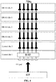
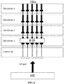
FIG. 4 is a schematic diagram of a method for testing a memory according to an embodiment of the disclosure. -
FIG. 5 is a schematic diagram of a method for testing a memory according to an embodiment of the disclosure. -
FIG. 6 is a schematic diagram of a method for testing a memory according to an embodiment of the disclosure. -
FIG. 7 is a schematic diagram of a method for testing a memory according to an embodiment of the disclosure. -
FIG. 8 is a schematic diagram of a method for testing a memory according to an embodiment of the disclosure. -
FIG. 9 is a schematic diagram of a method for testing a memory according to an embodiment of the disclosure. -
FIG. 10 is a schematic diagram of a method for testing a memory according to an embodiment of the disclosure. -
FIG. 11 is a schematic diagram of a device for testing a memory according to an embodiment of the disclosure. - Exemplary implementations are comprehensively described with reference to the accompanying drawings. However, the exemplary implementations in this specification can be implemented in various forms, and should not be construed as being limited to the embodiments set forth herein. On the contrary, these provided implementations may make the disclosure more comprehensive and complete, and the concepts of the exemplary implementations may be comprehensively conveyed to those skilled in the art. Same reference signs in the figures represent same or similar parts, and therefore are not repeatedly described. The accompanying drawings are merely schematic diagrams of the present specification and are not necessarily drawn to scale.
- Although relative terms such as "above" and "under" are used in the specification to describe a relative relationship of a component with a reference sign to another component with a reference sign, these terms are used in the specification for convenience only, for example, for indicating directions in the examples described according to the accompanying drawings. It can be understood that if a device with a reference sign is inverted, a component described to be "above" may become a component described to be "under." When a structure is "above" another structure, it may mean that the structure is integrated onto the another structure, or that the structure may be "directly" disposed on the another structure, or that the structure may be "indirectly" disposed on the another structure by using another structure.
- The terms of "one", "a", and "the" are used to indicate an existence of one or more elements/components/etc. The terms of "include" and "have" are used to indicate open inclusion and the existence of an element/a component/etc., in addition to the listed element/component/etc. The terms such as "first" and "second" are merely used as a sign and constitute no limitation on the number of its object.
-
FIG. 2 is a schematic flowchart of a method for testing a memory according to an embodiment of the disclosure. As shown inFIG. 2 , the method provided in this embodiment of the disclosure includes the following steps of S210 to S260. - In some embodiments, the method may be performed by a self-test circuit. The self-test circuit may be an internal circuit with a test capability in a storage device, and therefore may also be referred to as a built-in self-test (BIST) circuit. The BIST circuit may be disposed in a control die of a storage device corresponding to a to-be-tested memory, or may be disposed in a memory die such as a DRAM die in the storage device. This is not limited in the disclosure.
- In step of S210, a test instruction is obtained.
- In some embodiments, the self-test circuit may include a First-In-First-Out (FIFO) queue.
- The step of obtaining the test instruction may include buffering a command signal from an automatic test equipment (ATE) in the FIFO queue. An operating frequency of the test clock signal may be higher than a frequency of a clock signal output by the ATE. Alternatively, a frequency of the test clock signal may be equal to the frequency of the clock signal output by the ATE, and a phase of the test clock signal may be different from a phase of the clock signal output by the ATE. Then, the test instruction may be obtained by reading the command signal from the FIFO queue.
- According to embodiments of the disclosure, the data sent by the ATE to the BIST circuit can be buffered in the built-in FIFO queue in the BIST circuit. On one hand, the problem of frequency mismatch between a low-speed clock of the ATE and a high-speed clock of the BIST circuit may be resolved, thereby preventing the data sent by the ATE to the BIST circuit from being lost. Even if the ATE and the BIST circuit use the same clock frequency, phase inconsistency between the ATE and the BIST circuit may also cause the data loss. On the other hand, the data in of the BIST circuit, to avoid frequent bus operations and reduce the burden on the central processing unit.
- In some embodiments of the disclosure, the step of reading the command signal from the FIFO queue may include: obtaining third configuration information from the ATE; determining a reading frequency of the command signal based on the third configuration information; and in response to the reading frequency being equal to the frequency of the test clock signal, reading the command signal from the FIFO queue based on the test clock signal.
- In some embodiments of the disclosure, the step of reading the command signal from the FIFO queue may further include: in response to the reading frequency being equal to the frequency of the clock signal output by the ATE, reading the command signal from the FIFO queue based on the clock signal output by the ATE.
- In some embodiments of the disclosure, the ATE may send the third configuration information to the BIST circuit to specify the frequency of reading the buffered command signal from the FIFO queue in the BIST circuit. It may be specified that the buffered command signal is read from the FIFO queue in the BIST circuit based on a high-speed clock generated by the BIST circuit or based on a low-speed clock of the ATE. This is not limited in the disclosure.
- In some embodiments of the disclosure, the step of obtaining the test instruction may further include: determining a target operating mode of the self-test circuit; and parsing the command signal based on the target operating mode and determining the command signal to be the test instruction.
- In some embodiments of the disclosure, the step of determining the target operating mode of the self-test circuit may include: obtaining first configuration information from the ATE; and determining the target operating mode based on the first configuration information.
- In some embodiments, since the BIST circuit has a limited quantity of command pins, and the quantity of instructions represented by the parsed command signals is limited, the various command signals sent by the ATE to the BIST circuit may not be effectively represented. Therefore, different operating modes may be set. In the different operating modes, a same pin signal may represent different command signals according to the different operating modes, so that the limited command pins may be reused to parse more different command signals. For example, an AND gate, one of the simplest gates, may have two input pins, which may represent only four different command signals: "11", "01", "10", and "00". When different operating modes are introduced, "11", "01", "10", and "00" may respectively represent more instructions. For example, in a first operating mode (e.g., a test mode in which a DRAM die is tested), "11", "01", "10", and "00" may respectively represent four different instructions during the test of the DRAM die. For example, in a second operating mode (e.g., a test mode in which a control die is tested), "11", "01", "10", and "00" may respectively represent four different instructions during the test of the control die. The examples herein are merely used for description, and actual types, quantities, control logic of the operating modes may be determined based on an actual need and are not limited in the disclosure.
- In the step of S220, in response to the test instruction, a test clock signal, a to-be-tested address and to-be-tested data are generated.
- In some embodiments, the self-test circuit may further include a clock signal generator. A clock signal output by the clock signal generator that is built in the BIST circuit may be configured to test the memory, and therefore the clock signal may also be referred to as the test clock signal. The clock signal generator may generate a high-speed clock signal by using a low-speed clock signal of the ATE, and therefore the clock signal generator may also be referred to as a high-speed clock generator. In some embodiments, "low-speed" and "high-speed" are relative terms, that is, a frequency of the clock signal generated by the BIST circuit may be higher than a frequency of the clock signal generated by the ATE. Therefore, the clock signal generated by the ATE may be referred to as the low-speed clock signal, and the clock signal generated by the BIST circuit may be referred to as the high-speed clock signal. A specific frequency value may be determined based on an actual situation of the tested DRAM die and is not limited in the disclosure.
- The method for testing the memory may further include obtaining second configuration information from the ATE; determining the frequency of the test clock signal based on the second configuration information; and generating a test clock signal that has the frequency of the test clock signal by using the clock signal generator.
- When performing the method, the BIST circuit may use a computer to generate various pieces of to-be-tested data for testing a to-be-tested memory by using a to-be-tested data generation algorithm. The ATE may read the to-be-tested data from the computer and send the to-be-tested data to the BIST circuit; then, the BIST circuit may send the to-be-tested data to the to-be-tested memory for testing. Alternatively, the to-be-tested data generation algorithm may be built in the ATE or the BIST circuit, and the ATE or the BIST circuit may generate the to-be-tested data by itself. When a plurality of memory dies in the storage device corresponding to the control die share a peripheral pin, one or more memory dies to which the to-be-tested data is to be sent may need to be firstly determined from the plurality of memory dies. In this case, the ATE may firstly send the obtained to-be-tested data to the control die, and the control die may determine which of the memory dies as the to-be-tested memory. And then, the received to-be-tested data may be sent to the to-be-tested memory for testing. As such, the ATE may test the plurality of memory dies in parallel by using a small quantity of peripheral pins of the storage device, without being limited by the quantity of peripheral pins of the storage device.
- In the step of S230, a to-be-tested memory is determined from memories of a storage device. The storage device includes a self-test circuit.
- In some embodiments of the disclosure, the step of determining the to-be-tested memory from the memories of the storage device may include: obtaining fourth configuration information from the ATE; and determining the to-be-tested memory based on the fourth configuration information. The to-be-tested memory may be one or more target memories in the storage device.
- In some embodiments of the disclosure, the ATE may send the fourth configuration information to the BIST circuit to specify to test a specific memory in the storage device, or test all of or some of the memories in parallel. The BIST circuit may simultaneously test all of the memory dies in the storage device, thereby reducing the test time, improving the test efficiency, and reducing the test cost.
- In some embodiments of the disclosure, the storage device may further include a control die, and the self-test circuit may be arranged in the control die.
- In some embodiments of the disclosure, the memories of the storage device may be vertically stacked above or beneath the control die. Alternatively, the memories of the storage device may be horizontally interconnected to the control die. The disclosure will not be limited in this regard.
- In some embodiments of the disclosure, the to-be-tested memory may include a plurality of memory dies, and the plurality of memory dies may belong to a same storage device. Additionally, the control die and the plurality of memory dies may also belong to the same storage device. In some embodiments of the disclosure, the plurality of memory dies of the to-be-tested memory may be vertically stacked above the control die successively. In some other embodiments of the disclosure, the plurality of memory dies of the to-be-tested memory may be vertically stacked beneath the control die successively. In other embodiments of the disclosure, the plurality of memory dies of the to-be-tested memory may be vertically stacked successively, and the plurality of memory dies vertically stacked successively may be horizontally interconnected to the control die. In some other embodiments of the disclosure, the plurality of memory dies of the to-be-tested memory and the control die may be horizontally distributed above the storage device. This will not be limited in the disclosure.
- In some embodiments of the disclosure, the self-test circuit may be arranged in the memories of the storage device. The BIST circuit may also be disposed in any memory in the storage device in which the to-be-tested memory is arranged.
- In some embodiments of the disclosure, the to-be-tested memory may be any type of memory, for example, a DRAM or a Static Random-Access Memory (SRAM). The to-be-tested memory may be one of, some of, or all of the memory dies in the storage device.
- In the step of S240, the to-be-tested data is written into a storage unit corresponding to a to-be-tested address of the to-be-tested memory.
- In some embodiments of the disclosure, the BIST circuit may write the to-be-tested data into the storage unit corresponding to the to-be-tested address of the to-be-tested memory according to the test clock signal generated in the foregoing steps.
- In some embodiments of the disclosure, the step of writing the to-be-tested data into the storage unit corresponding to the to-be-tested address of the to-be-tested memory may include: in response to the to-be-tested memory being one target memory in the storage device, writing the to-be-tested data into a storage unit corresponding to a to-be-tested address of the target memory.
- In some embodiments of the disclosure, when a certain memory in the storage device is specified by the BIST circuit for testing, the BIST circuit may write the to-be-tested data into storage units of the memory successively. For example, in response to the specified memory being a first memory in the storage device and the first memory having 10,000 storage units, the BIST circuit may write a first bit of the to-be-tested data into a first storage unit of the first memory, and write a second bit of the to-be-tested data into a second storage unit of the first memory, and so on.
- In some embodiments of the disclosure, the step of writing the to-be-tested data into the storage unit corresponding to the to-be-tested address of the to-be-tested memory may include: in response to the to-be-tested memory being a plurality of target memories in the storage device, writing each of the to-be-tested data into storage units corresponding to a to-be-tested address of a respective one of the plurality of target memories.
- In some embodiments of the disclosure, the BIST circuit may test all of the memories in the storage device in parallel; then, the BIST circuit may respectively write the to-be-tested data into the storage units of the memories successively. For example, when there are a total of four memories and each having 10,000 storage units, the BIST circuit may respectively write the first bit in the to-be-tested data into the first storage units of the four memories, and then respectively write the second bit in the to-be-tested data into the second storage units of the four memories, and so on.
- In the step of S250, output data from the storage unit corresponding to the to-be-tested address of the to-be-tested memory is read.
- In some embodiments of the disclosure, the BIST circuit may read the output data from the storage unit corresponding to the to-be-tested address of the to-be-tested memory based on the test clock signal generated in the foregoing step.
- In the step of step S260, the to-be-tested data is compared with the output data corresponding to the to-be-tested address, to obtain a test result of the to-be-tested memory.
- In some embodiments of the disclosure, the step of comparing the to-be-tested data and the output data corresponding to the to-be-tested address, to obtain the test result of the to-be-tested memory may include: comparing the to-be-tested data with the output data corresponding to the to-be-tested address, to obtain a comparison result; and in response to the comparison result being not matching, recording the to-be-tested address corresponding to the to-be-tested data as an incorrect address. The test result may include the incorrect address.
- In an embodiment of the disclosure, the BIST circuit may be configured to test the to-be-tested memory. For example, the BIST circuit may input known character strings consisting of "0" and/or "1" to the storage units corresponding to addresses of the to-be-tested memory. After a certain delay, the BIST circuit may read the character strings from the storage units corresponding to the addresses, and successively perform an exclusive OR operation on the character strings that are previously input and the character strings that are subsequently read, to determine whether a specific storage unit has an error. In this case, an address of the storage unit having the error may be recorded; that is, a test result of the to-be-tested memory may include the address corresponding to the storage unit having the error in the to-be-tested memory, which may be referred to as the incorrect address.
- In some embodiments of the disclosure, the self-test circuit may include a volatile storage unit (i.e., a Volatile Memory) and a non-volatile storage unit (i.e., a Non-volatile Memory). The method may further include writing the test result of the to-be-tested memory into the volatile storage unit; and writing the test result in the volatile storage unit into the non-volatile storage unit for storage.
- In some embodiments of the disclosure, considering that the non-volatile storage unit has a low data writing speed when writing data and a high-speed clock signal is used by the BIST circuit when testing the to-be-tested memory, the generated test result may firstly be written into the volatile storage unit to prevent the test result from being lost. Since the data writing speed of the volatile storage unit is greater than the data writing speed of the non-volatile storage unit, the loss of the test result data can be effectively avoided. Additionally, considering that data in the volatile storage unit may be lost after the volatile storage unit is powered off, the test result in the volatile storage unit may be periodically written into the non-volatile storage unit for storage.
- In some embodiments of the disclosure, the self-test circuit may include a non-volatile storage unit, and the non-volatile storage unit may be configured to store an incorrect address of the to-be-tested memory. And the step of generating, in response to the test instruction, the to-be-tested address may include: obtaining the incorrect address stored in the non-volatile storage unit; and skipping automatically the incorrect address when generating the to-be-tested address.
- During an actual testing process, a same storage device or a same memory may be tested multiple times. To avoid repeatedly testing the same storage unit of the same memory, test results obtained in one or all previous test processes may be stored in the non-volatile storage unit. During a current testing, the storage units that have been tested may be firstly identified according to the test results stored in the non-volatile storage unit. In this case, the incorrect address may be automatically skipped when generating the to-be-tested address, to improve the test efficiency and avoid a waste of test resources.
- In an actual design scenario of the storage device, a separate redundancy area may need to be designated in each memory, to store a test result of the memory in the testing process, such as the foregoing incorrect address. Therefore, the design area of the memory is used, and the redundancy area in each memory may need to be designed, which will increase the complexity of the control and architecture of the storage device. In some embodiments, the non-volatile storage unit may be provided in the BIST circuit, and the provided non-volatile storage unit may be configured to store the test results of all the memories in the storage device. Therefore, each memory in the storage device does not need to separately design its own redundant area, so that a volume of the storage device may be reduced, the structure and design of the storage device can be simplified.
- In some embodiments of the disclosure, the BIST circuit may further analyze a cause of the error according to the obtained test result of the to-be-tested memory, to identify repairing information for repairing the storage unit having the error. The test result of the to-be-tested memory may include the address (i.e., the incorrect address) corresponding to the storage unit having the error in the to-be-tested memory and the repairing information for repairing the storage unit corresponding to the incorrect address. In other embodiments of the disclosure, the repairing information of the to-be-tested memory may further include spare circuit information in the to-be-tested memory. The spare circuit information may refer to some redundant spare storage units in the memory to ensure the reliability, in addition to the storage units conventionally designed to store data. For example, 200 spare storage units may be added to a first memory, in addition to conventional 10,000 storage units included in the first memory. During a testing process or an actual application process, in response that an error is found in the conventional 10,000 storage units, a faulty storage unit may be directly replaced by a spare storage unit. The replacement may refer to a replacement of the address of the storage unit instead of a physical replacement. Alternatively, while repairing the storage unit having the error, the spare storage unit may be used to replace the storage unit having the error before the repairing process is completed to maintain the normal functionality of the memory.
- According to the method for testing the memory disclosed in some embodiments of the disclosure, on one hand, the self-test circuit is added and used to complete the memory testing process, so that a whole wafer may be tested by using a small quantity of DA pads in one touch down. On the other hand, the self-test circuit is used to generate a high-speed clock for the memory testing, so that a high-speed memory test can be conducted by using a low-speed ATE, thereby reducing the test time and the test cost.
- An example is provided below to explain the method for testing the memory in greater details. The storage device is a DRAM in the example below. It is apparent that the method for testing the memory may be applicable to other types of memories, which will not be limited in the disclosure.
-
FIG. 3 is a schematic diagram of a method for testing a memory according to an embodiment of the disclosure. As shown inFIG. 3 , a storage device includes four DRAM dies (DRAM dies 0 to 3) which are stacked above a control die, and the four DRAM dies may be electrically connected through Through-Silicon Vias (TSVs). - The control die may include a BIST circuit, and the DRAM dies 0 to 3 may be vertically stacked above the control die successively. In the stacked storage device, several DRAM dies may be vertically stacked together. Compared with a conventional storage device, the stacked storage device has advantages in line layout, bandwidth, and latency, etc. The stacked storage device may not only occupy less space compared to the conventional storage device, but also may have a shorter die spacing, resulting in a shorten signal transmission path and a less signal delay. In the stacked storage device, the TSV technology may be used to perforate vias in the edges or specific positions of the DRAM dies, and these vias may be used as pathways for wiring and completing vertical interconnection.
- In a storage device with a stacked structure, although vertical stacked structure allows a higher density of memory dies in the same space, it also makes it is difficult for a control die to manage the memory dies. Therefore, in the embodiments shown in
FIGS. 4 and5 , a new level of control mechanism may be introduced in addition to the original level of control mechanism. As shown inFIGS. 4 and5 , each TSV memory die may have an independent base/logic die (a control die 2) at a bottom layer, which integrates DRAM dies to manage the entire cluster of the stacked structure. The base/logic die may directly communicate with a control die 1 in a Graphics Processing Unit (GPU)/ a Central Processing Unit (CPU)/ a System on a chip (Soc), etc., and may be configured to collect data in the stacked DRAM dies and help the control die 1 in the GPU/CPU/Soc manage the stacked DRAM dies. In the stacked system, it is not necessary to significantly change the scale of the control die 1 such as the GPU/CPU/Soc. The control die 1 such as the GPU/CPU/Soc, may only need to interact with the control die 2 in the base/logic die, and the control die 2 can manage each layer of the DRAM die in each cluster. - In the embodiment shown in
FIG. 4 , the BIST circuit may be disposed in the control die 1. In the embodiment shown inFIG. 5 , the BIST circuit may be disposed in the control die 2. Regardless its position, the BIST circuit can test, in series or in parallel, any one or more of the DRAM dies stacked on the BIST circuit. -
FIGS. 6 ,7, and 8 are schematic diagrams of a method for testing a memory according to some embodiments of the disclosure. - The difference between the embodiment shown in
FIG. 6 and that shown inFIG. 3 is that the BIST circuit inFIG. 6 may be disposed in any one of the DRAM dies that are vertically stacked on the control die. An example in which the BIST circuit is disposed on the DRAM die 3 is shown inFIG. 6 . The BIST circuit herein may also perform the method for testing the memory as described in the foregoing embodiments. - The difference between an embodiment shown in
FIG. 7 and that shown inFIG. 3 is that, inFIG. 7 , the DRAM dies 0 to 3 may be vertically stacked successively, and the vertically stacked DRAM dies 0 to 3 may be horizontally interconnected to the control die through a TSV adapter board. The BIST circuit ofFIG. 7 may also perform the method for testing the memory described in the foregoing embodiments. - The difference between an embodiment shown in
FIG. 8 and that shown inFIG. 3 is that, inFIG. 8 , the DRAM dies 0 to 3 and the control die may be all horizontally distributed on a substrate of the same storage device. The BIST circuit ofFIG. 8 may also perform the method for testing the memory described in the foregoing embodiments. -
FIG. 9 shows an example in which the BIST circuit is disposed on the control die in the storage device. As shown inFIG. 9 , the BIST circuit may include a BIST configuration circuit, a high-speed clock generator, a FIFO queue, a command decoder, a command execution circuit, a BIST control circuit, a non-volatile storage unit, a volatile storage unit, and a comparison unit. - Referring to
FIG. 9 , the BIST configuration circuit may be configured to receive configuration information from the ATE. The configuration information may include a frequency of a clock signal, an adopted operating mode, information about whether one memory or all memories are currently tested when the BIST circuit performing the test. The BIST configuration circuit may be connected to the high-speed clock generator, and may send, to the high-speed clock generator, a frequency of a test clock signal that currently needs to be generated, so that the high-speed clock generator may generate a test clock signal of the corresponding frequency based on the frequency. The BIST configuration circuit may be further connected to the command decoder, and may send a currently specified target operating mode to the command decoder, so that the command decoder may parse a received command signal from the ATE based on the currently specified target operating mode. The BIST configuration circuit may be further connected to the BIST control circuit, and may send, to the BIST control circuit, information about whether one of, some of, or all of the memories are currently tested, so that the BIST control circuit may determine a to-be-tested memory based on the information. - Continuing refer to
FIG. 9 , the high-speed clock generator may be respectively connected to the command execution circuit, the comparison unit, and the BIST control circuit, and then respectively output a test clock signal to the command execution circuit, the comparison unit, and the BIST control circuit. Therefore, the command execution circuit, the comparison unit, and the BIST control circuit may test the to-be-tested memory based on the test clock signal. - In some embodiments of the disclosure, the high-speed clock generator may use, for example, a Phase Locked Loop (PLL), which will not be limited in the disclosure.
- In the embodiment shown in
FIG. 9 , the FIFO queue may receive and buffer various command signals from the ATE through the DA pads. The command signals may include, but not limited to, a timing set command such as a timing interval/event, signals timing adjust such as an add/reduce CS delay, a normal command such as Active/Precharge, a test mode of DRAM die command (since the BIST circuit needs to use a test mode of the DRAM die to perform a DRAM test), an event loop control command, a voltage/current set/measure command; a MISC command such as a BIST Config command, a reading BIST result command, or a repairing DRAM command, etc. When the FIFO queue is empty, the command execution circuit may stop performing the test process. - In some embodiments of the disclosure, the command decoder may be respectively connected to the FIFO queue, the BIST configuration circuit, and the command execution circuit. And the command decoder may read the command signal from the FIFO queue according to a clock signal output by the ATE, and then parse the read command signal according to the target operating mode output by the BIST configuration circuit to interpret the command signal. When the parsed command signal indicates that a DRAM die is to be tested, the command decoder may send the parsed command signal to the command execution circuit to notify the command execution circuit to start testing the DRAM die.
- After receiving the signal from the command decoder, the command execution circuit may generate, according to a to-be-tested data generation algorithm built in the command execution circuit, to-be-tested data configured to test the DRAM die, generate to-be-tested address successively based on the test clock signal, and then send the to-be-tested data and the to-be-tested addresses thereof to the BIST control circuit.
- After receiving the to-be-tested data and the to-be-tested address from the command execution circuit, the BIST control circuit may determine, according to information sent by the BIST configuration circuit, whether the current to-be-tested memory is a certain target memory or all of the memories. Then, in response to the to-be-tested memory being the certain target memory, the BIST control circuit may write the to-be-tested data into storage units corresponding to to-be-tested address of the target memory according to the test clock signal. Alternatively, in response to the to-be-tested memory being all of the memories, the BIST control circuit may respectively write the to-be-tested data into the storage units corresponding to to-be-tested address of the memories according to the test clock signal.
- The BIST control circuit may send the to-be-tested data to the to-be-tested DRAM die, then read output data from the storage units corresponding to the to-be-tested address, and input the output data to the comparison unit.
- The comparison unit may obtain the to-be-tested address and the corresponding to-be-tested data thereof from the command execution circuit, perform one-to-one comparison on the output data and the to-be-tested data of the corresponding to-be-tested address, record a to-be-tested address corresponding to a storage unit with an inconsistent comparison result, and write the to-be-tested address into a volatile storage unit as an incorrect address.
- The incorrect address stored in the volatile storage unit may be written into a non-volatile storage unit for storage.
- When the storage device is tested again, the command execution circuit may firstly read the incorrect address that is previously recorded from the non-volatile storage unit, and then automatically skip the to-be-tested address that have been previously tested when generating a current to-be-tested address. As such, the storage unit corresponding to the incorrect address may be prevented from being repeatedly tested, thereby reducing computing resource consumption.
- In some embodiments of the disclosure, a test result stored in the non-volatile storage unit may be further provided externally, for example, to the control die or the ATE, to notify of a specific storage unit having an error, so that the storage unit may be repaired or replaced.
-
FIG. 10 is a schematic diagram of a method for testing a memory according to an embodiment of the disclosure. The difference between the embodiment shown inFIG. 10 and that shown inFIG. 9 is that, inFIG. 10 , the test clock signal generated by the high-speed clock generator may be directly provided to the command decoder, so that the command decoder may read the command signal from the FIFO queue based on the test clock signal. - According to the method for testing the memory provided in this embodiment of the disclosure, the BIST circuit is configured to test the memory, so that a high-speed clock needed for testing a DRAM may be generated by the high-speed clock generator, such as a PLL, built in the BIST circuit. Therefore, a low-speed clock of the machine may be used to generate a high-speed clock used by the BIST circuit, so that a whole wafer may be tested in one touch down, thereby reducing the test cost and the test time. The ATE may further program the BIST circuit through a small quantity of DA pads, and a command of the ATE may be parsed into a configuration of the BIST circuit, such as a DRAM test mode command, for execution. In addition, the method provided in some embodiments of the disclosure, a same TSV path may be used when accessing the DRAM die and during a normal operation, and the test time sequence is closer to that for the normal operation of the DRAM die. Furthermore, the BIST circuit may simultaneously test all DRAM dies in a stack, thereby reducing the test time.
-
FIG. 11 is a schematic diagram of a device for testing a memory according to an embodiment of the disclosure. As shown inFIG. 11 , in some embodiments of the disclosure, thedevice 1 may include a testinstruction obtaining unit 11, an addressdata generation unit 12, a to-be-testedmemory determination unit 13, a to-be-testeddata writing unit 14, an outputdata reading unit 15, and a testresult obtaining unit 16. - The test
instruction obtaining unit 11 is configured to obtain a test instruction. The addressdata generation unit 12 is configured to generate, in response to the test instruction, a test clock signal, a to-be-tested address and to-be-tested data. The to-be-testedmemory determination unit 13 is configured to determine a to-be-tested memory from memories of a storage device. The storage device includes a self-test circuit. The to-be-testeddata writing unit 14 is configured to write the to-be-tested data into a storage unit corresponding to a to-be-tested address of the to-be-tested memory. The outputdata reading unit 15 is configured to read output data from the storage unit corresponding to the to-be-tested address of the to-be-tested memory. The testresult obtaining unit 16 is configured to compare the to-be-tested data with the output data corresponding to the to-be-tested address, to obtain a test result of the to-be-tested memory. - In some embodiments of the disclosure, the self-test circuit may include a FIFO queue. The test
instruction obtaining unit 11 may include: a buffering unit, which may be configured to buffer a command signal from an ATE in the FIFO queue. An operating frequency of the test clock signal is higher than a frequency of a clock signal output by the ATE; alternatively, a frequency of the test clock signal is equal to the frequency of the clock signal output by the ATE, and a phase of the test clock signal is different from a phase of the clock signal output by the ATE. The testinstruction obtaining unit 11 may further include a signal reading unit, which may be configured to read the command signal from the FIFO queue. - In some embodiments of the disclosure, the test
instruction obtaining unit 11 may further include: a mode determination unit, which may be configured to determine a target operating mode of the self-test circuit. The testinstruction obtaining unit 11 may further include a command parsing unit, which may be configured to parse the command signal based on the target operating mode, and determine the command signal to be the test instruction. - In some embodiments of the disclosure, the mode determination unit may include: a first configuration information obtaining unit, which may be configured to obtain first configuration information from the ATE. And the mode determination unit may further include a target operating mode determination unit, which may be configured to determine the target operating mode based on the first configuration information.
- In some embodiments of the disclosure, the self-test circuit may further include a clock signal generator. The
test device 1 may further include: a second configuration information obtaining unit, which may be configured to obtain second configuration information from the ATE. Thetest device 1 may further include a test frequency determination unit, which may be configured to determine the frequency of the test clock signal based on the second configuration information. And thetest device 1 may further include a test clock generation unit, which may be configured to generate, by using the clock signal generator, a test clock signal that has the frequency of the test clock signal. - In some embodiments of the disclosure, the signal reading unit may include: a third configuration information obtaining unit, which may be configured to obtain third configuration information from the ATE. The signal reading unit may further include a reading frequency determination unit, which may be configured to determine a reading frequency of the command signal based on the third configuration information. And the signal reading unit may further include a first command signal reading unit, which may be configured to: in response to the reading frequency being equal to the frequency of the test clock signal, read the command signal from the FIFO queue based on the test clock signal.
- In some embodiments of the disclosure, the signal reading unit may further include: a second command signal reading unit, which may be configured to: in response to the reading frequency being equal to the frequency of the clock signal output by the ATE, read the command signal from the FIFO queue based on the clock signal output by the ATE.
- In some embodiments of the disclosure, the to-be-tested
memory determination unit 13 may include: a fourth configuration information obtaining unit, which may be configured to obtain fourth configuration information from the ATE. And the to-be-testedmemory determination unit 13 may further include a to-be-tested memory device determination unit, which may be configured to determine the to-be-tested memory based on the fourth configuration information. The to-be-tested memory may be one or more target memories in the storage device. - In some embodiments of the disclosure, the to-be-tested
data writing unit 14 may include a first writing unit, which may be configured to: in response to the to-be-tested memory being one target memory in the storage device, write the to-be-tested data into a storage unit corresponding to a to-be-tested address of the target memory. - In some embodiments of the disclosure, the to-be-tested
data writing unit 14 may further include: a second writing unit, which may be configured to: in response to the to-be-tested memory being a plurality of target memories in the storage device, write each of the to-be-tested data into storage units corresponding to a to-be-tested address of a respective one of the plurality of target memories. - In some embodiments of the disclosure, the test
result obtaining unit 16 may include: a comparison result obtaining unit, which may be configured to compare the to-be-tested data with the output data corresponding to the to-be-tested address, to obtain a comparison result. And the testresult obtaining unit 16 may further include an incorrect address recording unit, which may be configured to: in response to the comparison result being not matching, record the to-be-tested address corresponding to the to-be-tested data as an incorrect address, where the test result may include the incorrect address. - In some embodiments of the disclosure, the self-test circuit may include a volatile storage unit and a non-volatile storage unit. The
test device 1 may further include: a test result buffering unit, which may be configured to write the test result of the to-be-tested memory into the volatile storage unit. And thetest device 1 may further include a test result storage unit, which may be configured to write the test result in the volatile storage unit into the non-volatile storage unit for storage. - In some embodiments of the disclosure, the self-test circuit may include a non-volatile storage unit, and the non-volatile storage unit may be configured to store an incorrect address of the to-be-tested memory. The address
data generation unit 12 may include an incorrect address obtaining unit, which may be configured to obtain the incorrect address stored in the non-volatile storage unit. And the addressdata generation unit 12 may further include a to-be-tested address generation unit, which may be configured to skip automatically the incorrect address when generating the to-be-tested address. - In some embodiments of the disclosure, the storage device may further include a control die, and the self-test circuit may be arranged in the control die.
- In some embodiments of the disclosure, the memories of the storage device may be vertically stacked above or beneath the control die.
- In some embodiments of the disclosure, the self-test circuit may be arranged in the memories of the storage device.
- In some embodiments of the disclosure, the
test device 1 may be disposed in the self-test circuit. - The disclosure further provides an electronic device. The electronic device includes one or more processors and a storage device, the storage device being configured to store one or more programs. Upon being executed by the one or more processors, the one or more programs may cause the one or more processors to perform the method according to any one of the foregoing embodiments.
- The disclosure further provides a computer-readable storage medium in which a computer program is stored. Upon being executed by a processor, the computer program may cause the method of any one of the foregoing embodiments to be performed. The foregoing method embodiments may be referred to for details, which will not be repeatedly presented herein for the sake of conciseness.
- Those skilled in the art can easily figure out other embodiments of the disclosure after considering the specification and practicing the invention that is disclosed herein. This application is intended to cover any variations, functions, or adaptive changes of the present invention. These variations, functions, or adaptive changes comply with general principles of the present invention and include common knowledge or a conventional technical means in the technical field that is not disclosed in the disclosure. The specification and the embodiments are merely considered as exemplary, and the actual scope and spirit of the disclosure are specified by the appended claims.
Claims (20)
- A method for testing a memory, comprising:obtaining a test instruction;generating, in response to the test instruction, a test clock signal, a to-be-tested address and to-be-tested data;determining a to-be-tested memory from memories of a storage device, the storage device comprising a self-test circuit;writing the to-be-tested data into a storage unit corresponding to a to-be-tested address of the to-be-tested memory;reading output data from the storage unit corresponding to the to-be-tested address of the to-be-tested memory; andcomparing the to-be-tested data with the output data corresponding to the to-be-tested address, to obtain a test result of the to-be-tested memory.
- The method for testing the memory of claim 1, wherein the self-test circuit comprises a first-in-first-out queue; and obtaining the test instruction comprises:buffering a command signal from an automatic test equipment in the first-in-first-out queue, wherein an operating frequency of the test clock signal is higher than a frequency of a clock signal output by the automatic test equipment, or, a frequency of the test clock signal is equal to the frequency of the clock signal output by the automatic test equipment, and a phase of the test clock signal is different from a phase of the clock signal output by the automatic test equipment; andreading the command signal from the first-in-first-out queue.
- The method for testing the memory of claim 2, wherein obtaining the test instruction further comprises:determining a target operating mode of the self-test circuit; andparsing the command signal based on the target operating mode and determining the command signal to be the test instruction.
- The method for testing the memory of claim 3, wherein determining the target operating mode of the self-test circuit comprises:obtaining, from the automatic test equipment, first configuration information; anddetermining, based on the first configuration information, the target operating mode.
- The method for testing the memory of claim 2, wherein the self-test circuit further comprises a clock signal generator, and the method further comprises:obtaining, from the automatic test equipment, second configuration information;determining, based on the second configuration information, the frequency of the test clock signal; andgenerating, by using the clock signal generator, a test clock signal that has the frequency of the test clock signal.
- The method for testing the memory of claim 2, wherein reading the command signal from the first-in-first-out queue comprises:obtaining, from the automatic test equipment, third configuration information;determining, based on the third configuration information, a reading frequency of the command signal; andin response to the reading frequency being equal to the frequency of the test clock signal, reading, based on the test clock signal, the command signal from the first-in-first-out queue.
- The method for testing the memory of claim 6, wherein reading the command signal from the first-in-first-out queue further comprises:
in response to the reading frequency being equal to the frequency of the clock signal output by the automatic test equipment, reading, based on the clock signal output by the automatic test equipment, the command signal from the first-in-first-out queue. - The method for testing the memory of claim 1, wherein determining the to-be-tested memory from the memories of the storage device comprises:obtaining, from the automatic test equipment, fourth configuration information; anddetermining, based on the fourth configuration information, the to-be-tested memory, the to-be-tested memory being one or more target memories in the storage device.
- The method for testing the memory of claim 8, wherein writing the to-be-tested data into the storage unit corresponding to the to-be-tested address of the to-be-tested memory comprises:
in response to the to-be-tested memory being one target memory in the storage device, writing the to-be-tested data into a storage unit corresponding to a to-be-tested address of the target memory. - The method for testing the memory of claim 8, wherein writing the to-be-tested data into the storage unit corresponding to the to-be-tested address of the to-be-tested memory comprises:
in response to the to-be-tested memory being a plurality of target memories in the storage device, writing each of the to-be-tested data into storage units corresponding to a to-be-tested address of a respective one of the plurality of target memories. - The method for testing the memory of claim 1, wherein comparing the to-be-tested data with the output data corresponding to the to-be-tested address, to obtain the test result of the to-be-tested memory comprises:comparing the to-be-tested data with the output data corresponding to the to-be-tested address, to obtain a comparison result; andin response to the comparison result being not matching, recording the to-be-tested address corresponding to the to-be-tested data as an incorrect address, the test result comprising the incorrect address.
- The method for testing the memory of claim 11, wherein the self-test circuit comprises a volatile storage unit and a non-volatile storage unit, and the method further comprises:writing the test result of the to-be-tested memory into the volatile storage unit; andwriting the test result in the volatile storage unit into the non-volatile storage unit for storage.
- The method for testing the memory of claim 1, wherein the self-test circuit comprises a non-volatile storage unit, configured to store an incorrect address of the to-be-tested memory; and generating, in response to the test instruction, the to-be-tested address comprises:obtaining the incorrect address stored in the non-volatile storage unit; andskipping automatically the incorrect address when generating the to-be-tested address.
- The method for testing the memory of claim 1, wherein the storage device further comprises a control die, the self-test circuit being arranged in the control die.
- The method for testing the memory of claim 14, wherein the memories of the storage device are vertically stacked above or beneath the control die.
- The method for testing the memory of claim 1, wherein the self-test circuit is arranged in the memories of the storage device.
- The method for testing the memory of claims 1, wherein the method is performed by the self-test circuit.
- A device for testing a memory, comprising:a test instruction obtaining unit, configured to obtain a test instruction;an address data generation unit, configured to generate, in response to the test instruction, a test clock signal, a to-be-tested address and to-be-tested data;a to-be-tested memory determination unit, configured to determine a to-be-tested memory from memories of a storage device, the storage device comprising a self-test circuit;a to-be-tested data writing unit, configured to write the to-be-tested data into a storage unit corresponding to a to-be-tested address of the to-be-tested memory;an output data reading unit, configured to read output data from the storage unit corresponding to the to-be-tested address of the to-be-tested memory; anda test result obtaining unit, configured to compare the to-be-tested data with the output data corresponding to the to-be-tested address, to obtain a test result of the to-be-tested memory.
- An electronic device, comprising:one or more processors; anda storage device, configured to store one or more programs, wherein upon being executed by the one or more processors, the one or more programs cause the one or more processors to perform the method of claim 1.
- A computer-readable storage medium storing a computer program, wherein upon being executed by a processor, the computer program causes the method of claim 1 to be performed.
Applications Claiming Priority (2)
| Application Number | Priority Date | Filing Date | Title |
|---|---|---|---|
| CN202010166581.1A CN113393887B (en) | 2020-03-11 | 2020-03-11 | Memory test method and related equipment |
| PCT/CN2020/114513 WO2021179559A1 (en) | 2020-03-11 | 2020-09-10 | Method for testing memory and related equipment |
Publications (3)
| Publication Number | Publication Date |
|---|---|
| EP3913632A1 true EP3913632A1 (en) | 2021-11-24 |
| EP3913632A4 EP3913632A4 (en) | 2022-05-11 |
| EP3913632B1 EP3913632B1 (en) | 2024-01-03 |
Family
ID=77615342
Family Applications (1)
| Application Number | Title | Priority Date | Filing Date |
|---|---|---|---|
| EP20918133.8A Active EP3913632B1 (en) | 2020-03-11 | 2020-09-10 | Method for testing memory and related equipment |
Country Status (4)
| Country | Link |
|---|---|
| US (1) | US11393553B2 (en) |
| EP (1) | EP3913632B1 (en) |
| CN (1) | CN113393887B (en) |
| WO (1) | WO2021179559A1 (en) |
Families Citing this family (17)
| Publication number | Priority date | Publication date | Assignee | Title |
|---|---|---|---|---|
| CN113393893A (en) * | 2020-03-11 | 2021-09-14 | 长鑫存储技术有限公司 | Memory test method and related equipment |
| WO2022060559A1 (en) * | 2020-09-18 | 2022-03-24 | Rambus Inc. | Methods and circuits for aggregating processing units and dynamically allocating memory |
| JP2023060606A (en) * | 2021-10-18 | 2023-04-28 | キオクシア株式会社 | Semiconductor integrated circuit and memory system |
| CN114171099A (en) * | 2021-10-26 | 2022-03-11 | 深圳市国微电子有限公司 | 3D stacked high-broadband memory multi-channel parallel test system and method |
| CN114035027B (en) * | 2021-11-10 | 2025-09-16 | 成都利普芯微电子有限公司 | MBIST circuit, driver chip, electronic equipment and test method |
| CN116583902A (en) * | 2021-12-08 | 2023-08-11 | 华为技术有限公司 | Memory, memory test method and electronic device |
| CN114528164B (en) * | 2022-01-14 | 2026-03-06 | 深圳市晶存科技股份有限公司 | DRAM testing methods, electronic devices and storage media |
| CN114550801B (en) * | 2022-02-25 | 2024-07-05 | 长鑫存储技术有限公司 | Testing method and testing device for memory chip, and electronic equipment |
| CN114649051B (en) * | 2022-03-22 | 2022-11-11 | 合肥悦芯半导体科技有限公司 | Memory test method, device and system |
| JP2023181864A (en) * | 2022-06-13 | 2023-12-25 | キオクシア株式会社 | Test system, test method, and test program |
| CN117334241A (en) * | 2022-06-23 | 2024-01-02 | 长鑫存储技术有限公司 | Test methods, test structures and memory |
| CN118351920A (en) * | 2023-01-06 | 2024-07-16 | 长鑫存储技术有限公司 | Memory and writing test method |
| US12424264B2 (en) | 2023-03-14 | 2025-09-23 | Powerchip Semiconductor Manufacturing Corporation | Stacked memory with a timing adjustment function |
| CN116417059A (en) * | 2023-03-17 | 2023-07-11 | 宁畅信息产业(北京)有限公司 | Memory batch test method and system |
| CN117079703B (en) * | 2023-10-17 | 2024-02-02 | 紫光同芯微电子有限公司 | Method and device for testing embedded memory of chip and electronic equipment |
| CN120260657B (en) * | 2025-06-03 | 2025-08-19 | 北京青耘科技有限公司 | Memory testing device, three-dimensional stacked memory chip, and memory testing method and system |
| CN121354648B (en) * | 2025-12-16 | 2026-04-03 | 极芯拓方技术(上海)有限公司 | A test circuit and memory |
Family Cites Families (14)
| Publication number | Priority date | Publication date | Assignee | Title |
|---|---|---|---|---|
| JP2001319500A (en) * | 2000-05-10 | 2001-11-16 | Mitsubishi Electric Corp | Semiconductor integrated circuit device |
| US7036064B1 (en) * | 2000-11-13 | 2006-04-25 | Omar Kebichi | Synchronization point across different memory BIST controllers |
| US7370256B2 (en) * | 2001-09-28 | 2008-05-06 | Inapac Technology, Inc. | Integrated circuit testing module including data compression |
| JP4229652B2 (en) * | 2002-07-19 | 2009-02-25 | 株式会社ルネサステクノロジ | Semiconductor circuit device |
| KR100528472B1 (en) * | 2003-03-13 | 2005-11-15 | 삼성전자주식회사 | Semiconductor memory device capable of internally generating variable clock signals according to modes of operation |
| US7159145B2 (en) * | 2003-05-12 | 2007-01-02 | Infineon Technologies Ag | Built-in self test system and method |
| CN100592096C (en) * | 2004-10-15 | 2010-02-24 | 创世纪微芯片公司 | Automated fault testing of logic blocks using internal real-speed logic - BIST |
| DE112006004263B4 (en) * | 2005-09-02 | 2015-05-13 | Google, Inc. | memory chip |
| JP5846679B2 (en) * | 2012-03-30 | 2016-01-20 | インテル・コーポレーション | Built-in self-test for stacked memory architecture |
| US9864007B2 (en) * | 2014-04-30 | 2018-01-09 | Duke University | Software-based self-test and diagnosis using on-chip memory |
| CN106556793B (en) * | 2016-11-09 | 2019-05-31 | 上海东软载波微电子有限公司 | Chip test system and test method |
| CN107068196A (en) * | 2017-05-09 | 2017-08-18 | 武汉新芯集成电路制造有限公司 | Built-in self-test circuit, system and method for flash memory |
| KR102471531B1 (en) * | 2017-12-21 | 2022-11-28 | 에스케이하이닉스 주식회사 | Semiconductor apparatus and system capable of performing high speed test in low speed operation environment |
| CN108899061B (en) * | 2018-07-20 | 2021-03-09 | 嘉楠明芯(北京)科技有限公司 | Memory built-in self-test method and system in power supply normally-open chip |
-
2020
- 2020-03-11 CN CN202010166581.1A patent/CN113393887B/en active Active
- 2020-09-10 EP EP20918133.8A patent/EP3913632B1/en active Active
- 2020-09-10 WO PCT/CN2020/114513 patent/WO2021179559A1/en not_active Ceased
-
2021
- 2021-06-23 US US17/355,946 patent/US11393553B2/en active Active
Also Published As
| Publication number | Publication date |
|---|---|
| CN113393887B (en) | 2022-04-12 |
| EP3913632B1 (en) | 2024-01-03 |
| EP3913632A4 (en) | 2022-05-11 |
| CN113393887A (en) | 2021-09-14 |
| US20210319844A1 (en) | 2021-10-14 |
| US11393553B2 (en) | 2022-07-19 |
| WO2021179559A1 (en) | 2021-09-16 |
Similar Documents
| Publication | Publication Date | Title |
|---|---|---|
| EP3913632B1 (en) | Method for testing memory and related equipment | |
| US11867758B2 (en) | Test method for control chip and related device | |
| US7484141B2 (en) | Semiconductor device capable of performing test at actual operating frequency | |
| KR100890749B1 (en) | Semiconductor device whereon memory chip and logic chip are mounted, making testing of memory chip possible | |
| TWI234784B (en) | Memory module and memory component built-in self test | |
| CN100399473C (en) | Built-in self-test system and method | |
| US20140078841A1 (en) | Programmable memory built in self repair circuit | |
| US11862268B2 (en) | Test method for control chip and related device | |
| US7237165B2 (en) | Method for testing embedded DRAM arrays | |
| KR20170036884A (en) | Repair circuit, semiconductor apparatus and semiconductor system using the same | |
| US10249380B2 (en) | Embedded memory testing with storage borrowing | |
| WO2007114373A1 (en) | Test method, test system, and auxiliary substrate | |
| US6807116B2 (en) | Semiconductor circuit device capable of accurately testing embedded memory | |
| KR20140013893A (en) | Method for training memory core at boot-up and memory system | |
| US12045150B2 (en) | Method for testing memory by built-in self-test storage space and related device | |
| US8674718B2 (en) | Built off testing apparatus | |
| US11693054B2 (en) | Computer-readable recording medium storing analysis program, analysis method, and analysis device | |
| EP3933843A1 (en) | Memory testing method and related device | |
| Lukka et al. | Review on BIST architectures of DRAMs | |
| KR100684548B1 (en) | System-on-Chip capable of self-function test and its functional test method | |
| JP2004022014A (en) | Semiconductor device and method for testing the same | |
| Ataei et al. | A unified memory compiler for synchronous and asynchronous circuits | |
| CN119229945A (en) | A system-on-chip embedded storage unit evaluation device | |
| CN119993247A (en) | A memory built-in self-test method, controller and circuit | |
| HK1063264B (en) | Memory module and memory component built-in self test and methods thereof |
Legal Events
| Date | Code | Title | Description |
|---|---|---|---|
| STAA | Information on the status of an ep patent application or granted ep patent |
Free format text: STATUS: UNKNOWN |
|
| STAA | Information on the status of an ep patent application or granted ep patent |
Free format text: STATUS: THE INTERNATIONAL PUBLICATION HAS BEEN MADE |
|
| PUAI | Public reference made under article 153(3) epc to a published international application that has entered the european phase |
Free format text: ORIGINAL CODE: 0009012 |
|
| STAA | Information on the status of an ep patent application or granted ep patent |
Free format text: STATUS: REQUEST FOR EXAMINATION WAS MADE |
|
| 17P | Request for examination filed |
Effective date: 20210819 |
|
| AK | Designated contracting states |
Kind code of ref document: A1 Designated state(s): AL AT BE BG CH CY CZ DE DK EE ES FI FR GB GR HR HU IE IS IT LI LT LU LV MC MK MT NL NO PL PT RO RS SE SI SK SM TR |
|
| REG | Reference to a national code |
Ref country code: DE Ref legal event code: R079 Free format text: PREVIOUS MAIN CLASS: G11C0029120000 Ipc: G11C0029140000 Ref document number: 602020024061 Country of ref document: DE |
|
| A4 | Supplementary search report drawn up and despatched |
Effective date: 20220413 |
|
| RIC1 | Information provided on ipc code assigned before grant |
Ipc: G11C 29/00 20060101ALN20220407BHEP Ipc: G11C 29/56 20060101ALI20220407BHEP Ipc: G11C 29/48 20060101ALI20220407BHEP Ipc: G11C 29/44 20060101ALI20220407BHEP Ipc: G11C 29/12 20060101ALI20220407BHEP Ipc: G11C 29/14 20060101AFI20220407BHEP |
|
| STAA | Information on the status of an ep patent application or granted ep patent |
Free format text: STATUS: EXAMINATION IS IN PROGRESS |
|
| 17Q | First examination report despatched |
Effective date: 20230124 |
|
| DAV | Request for validation of the european patent (deleted) | ||
| DAX | Request for extension of the european patent (deleted) | ||
| RIC1 | Information provided on ipc code assigned before grant |
Ipc: G11C 29/00 20060101ALN20230609BHEP Ipc: G11C 29/56 20060101ALI20230609BHEP Ipc: G11C 29/48 20060101ALI20230609BHEP Ipc: G11C 29/44 20060101ALI20230609BHEP Ipc: G11C 29/12 20060101ALI20230609BHEP Ipc: G11C 29/14 20060101AFI20230609BHEP |
|
| GRAP | Despatch of communication of intention to grant a patent |
Free format text: ORIGINAL CODE: EPIDOSNIGR1 |
|
| STAA | Information on the status of an ep patent application or granted ep patent |
Free format text: STATUS: GRANT OF PATENT IS INTENDED |
|
| INTG | Intention to grant announced |
Effective date: 20230727 |
|
| P01 | Opt-out of the competence of the unified patent court (upc) registered |
Effective date: 20230822 |
|
| GRAS | Grant fee paid |
Free format text: ORIGINAL CODE: EPIDOSNIGR3 |
|
| GRAA | (expected) grant |
Free format text: ORIGINAL CODE: 0009210 |
|
| STAA | Information on the status of an ep patent application or granted ep patent |
Free format text: STATUS: THE PATENT HAS BEEN GRANTED |
|
| AK | Designated contracting states |
Kind code of ref document: B1 Designated state(s): AL AT BE BG CH CY CZ DE DK EE ES FI FR GB GR HR HU IE IS IT LI LT LU LV MC MK MT NL NO PL PT RO RS SE SI SK SM TR |
|
| REG | Reference to a national code |
Ref country code: GB Ref legal event code: FG4D |
|
| REG | Reference to a national code |
Ref country code: CH Ref legal event code: EP |
|
| REG | Reference to a national code |
Ref country code: DE Ref legal event code: R096 Ref document number: 602020024061 Country of ref document: DE |
|
| REG | Reference to a national code |
Ref country code: IE Ref legal event code: FG4D |
|
| REG | Reference to a national code |
Ref country code: LT Ref legal event code: MG9D |
|
| PG25 | Lapsed in a contracting state [announced via postgrant information from national office to epo] |
Ref country code: ES Free format text: LAPSE BECAUSE OF FAILURE TO SUBMIT A TRANSLATION OF THE DESCRIPTION OR TO PAY THE FEE WITHIN THE PRESCRIBED TIME-LIMIT Effective date: 20240103 |
|
| PG25 | Lapsed in a contracting state [announced via postgrant information from national office to epo] |
Ref country code: ES Free format text: LAPSE BECAUSE OF FAILURE TO SUBMIT A TRANSLATION OF THE DESCRIPTION OR TO PAY THE FEE WITHIN THE PRESCRIBED TIME-LIMIT Effective date: 20240103 |
|
| REG | Reference to a national code |
Ref country code: NL Ref legal event code: MP Effective date: 20240103 |
|
| REG | Reference to a national code |
Ref country code: AT Ref legal event code: MK05 Ref document number: 1647639 Country of ref document: AT Kind code of ref document: T Effective date: 20240103 |
|
| PG25 | Lapsed in a contracting state [announced via postgrant information from national office to epo] |
Ref country code: NL Free format text: LAPSE BECAUSE OF FAILURE TO SUBMIT A TRANSLATION OF THE DESCRIPTION OR TO PAY THE FEE WITHIN THE PRESCRIBED TIME-LIMIT Effective date: 20240103 |
|
| PG25 | Lapsed in a contracting state [announced via postgrant information from national office to epo] |
Ref country code: NL Free format text: LAPSE BECAUSE OF FAILURE TO SUBMIT A TRANSLATION OF THE DESCRIPTION OR TO PAY THE FEE WITHIN THE PRESCRIBED TIME-LIMIT Effective date: 20240103 |
|
| PG25 | Lapsed in a contracting state [announced via postgrant information from national office to epo] |
Ref country code: IS Free format text: LAPSE BECAUSE OF FAILURE TO SUBMIT A TRANSLATION OF THE DESCRIPTION OR TO PAY THE FEE WITHIN THE PRESCRIBED TIME-LIMIT Effective date: 20240503 |
|
| PG25 | Lapsed in a contracting state [announced via postgrant information from national office to epo] |
Ref country code: LT Free format text: LAPSE BECAUSE OF FAILURE TO SUBMIT A TRANSLATION OF THE DESCRIPTION OR TO PAY THE FEE WITHIN THE PRESCRIBED TIME-LIMIT Effective date: 20240103 |
|
| PG25 | Lapsed in a contracting state [announced via postgrant information from national office to epo] |
Ref country code: GR Free format text: LAPSE BECAUSE OF FAILURE TO SUBMIT A TRANSLATION OF THE DESCRIPTION OR TO PAY THE FEE WITHIN THE PRESCRIBED TIME-LIMIT Effective date: 20240404 |
|
| PG25 | Lapsed in a contracting state [announced via postgrant information from national office to epo] |
Ref country code: HR Free format text: LAPSE BECAUSE OF FAILURE TO SUBMIT A TRANSLATION OF THE DESCRIPTION OR TO PAY THE FEE WITHIN THE PRESCRIBED TIME-LIMIT Effective date: 20240103 Ref country code: RS Free format text: LAPSE BECAUSE OF FAILURE TO SUBMIT A TRANSLATION OF THE DESCRIPTION OR TO PAY THE FEE WITHIN THE PRESCRIBED TIME-LIMIT Effective date: 20240403 |
|
| PG25 | Lapsed in a contracting state [announced via postgrant information from national office to epo] |
Ref country code: CZ Free format text: LAPSE BECAUSE OF FAILURE TO SUBMIT A TRANSLATION OF THE DESCRIPTION OR TO PAY THE FEE WITHIN THE PRESCRIBED TIME-LIMIT Effective date: 20240103 Ref country code: AT Free format text: LAPSE BECAUSE OF FAILURE TO SUBMIT A TRANSLATION OF THE DESCRIPTION OR TO PAY THE FEE WITHIN THE PRESCRIBED TIME-LIMIT Effective date: 20240103 |
|
| PG25 | Lapsed in a contracting state [announced via postgrant information from national office to epo] |
Ref country code: RS Free format text: LAPSE BECAUSE OF FAILURE TO SUBMIT A TRANSLATION OF THE DESCRIPTION OR TO PAY THE FEE WITHIN THE PRESCRIBED TIME-LIMIT Effective date: 20240403 Ref country code: NO Free format text: LAPSE BECAUSE OF FAILURE TO SUBMIT A TRANSLATION OF THE DESCRIPTION OR TO PAY THE FEE WITHIN THE PRESCRIBED TIME-LIMIT Effective date: 20240403 Ref country code: LT Free format text: LAPSE BECAUSE OF FAILURE TO SUBMIT A TRANSLATION OF THE DESCRIPTION OR TO PAY THE FEE WITHIN THE PRESCRIBED TIME-LIMIT Effective date: 20240103 Ref country code: IS Free format text: LAPSE BECAUSE OF FAILURE TO SUBMIT A TRANSLATION OF THE DESCRIPTION OR TO PAY THE FEE WITHIN THE PRESCRIBED TIME-LIMIT Effective date: 20240503 Ref country code: HR Free format text: LAPSE BECAUSE OF FAILURE TO SUBMIT A TRANSLATION OF THE DESCRIPTION OR TO PAY THE FEE WITHIN THE PRESCRIBED TIME-LIMIT Effective date: 20240103 Ref country code: GR Free format text: LAPSE BECAUSE OF FAILURE TO SUBMIT A TRANSLATION OF THE DESCRIPTION OR TO PAY THE FEE WITHIN THE PRESCRIBED TIME-LIMIT Effective date: 20240404 Ref country code: CZ Free format text: LAPSE BECAUSE OF FAILURE TO SUBMIT A TRANSLATION OF THE DESCRIPTION OR TO PAY THE FEE WITHIN THE PRESCRIBED TIME-LIMIT Effective date: 20240103 Ref country code: BG Free format text: LAPSE BECAUSE OF FAILURE TO SUBMIT A TRANSLATION OF THE DESCRIPTION OR TO PAY THE FEE WITHIN THE PRESCRIBED TIME-LIMIT Effective date: 20240103 Ref country code: AT Free format text: LAPSE BECAUSE OF FAILURE TO SUBMIT A TRANSLATION OF THE DESCRIPTION OR TO PAY THE FEE WITHIN THE PRESCRIBED TIME-LIMIT Effective date: 20240103 |
|
| PG25 | Lapsed in a contracting state [announced via postgrant information from national office to epo] |
Ref country code: PL Free format text: LAPSE BECAUSE OF FAILURE TO SUBMIT A TRANSLATION OF THE DESCRIPTION OR TO PAY THE FEE WITHIN THE PRESCRIBED TIME-LIMIT Effective date: 20240103 Ref country code: PT Free format text: LAPSE BECAUSE OF FAILURE TO SUBMIT A TRANSLATION OF THE DESCRIPTION OR TO PAY THE FEE WITHIN THE PRESCRIBED TIME-LIMIT Effective date: 20240503 |
|
| PG25 | Lapsed in a contracting state [announced via postgrant information from national office to epo] |
Ref country code: SE Free format text: LAPSE BECAUSE OF FAILURE TO SUBMIT A TRANSLATION OF THE DESCRIPTION OR TO PAY THE FEE WITHIN THE PRESCRIBED TIME-LIMIT Effective date: 20240103 Ref country code: PT Free format text: LAPSE BECAUSE OF FAILURE TO SUBMIT A TRANSLATION OF THE DESCRIPTION OR TO PAY THE FEE WITHIN THE PRESCRIBED TIME-LIMIT Effective date: 20240503 Ref country code: PL Free format text: LAPSE BECAUSE OF FAILURE TO SUBMIT A TRANSLATION OF THE DESCRIPTION OR TO PAY THE FEE WITHIN THE PRESCRIBED TIME-LIMIT Effective date: 20240103 Ref country code: LV Free format text: LAPSE BECAUSE OF FAILURE TO SUBMIT A TRANSLATION OF THE DESCRIPTION OR TO PAY THE FEE WITHIN THE PRESCRIBED TIME-LIMIT Effective date: 20240103 |
|
| REG | Reference to a national code |
Ref country code: DE Ref legal event code: R097 Ref document number: 602020024061 Country of ref document: DE |
|
| PG25 | Lapsed in a contracting state [announced via postgrant information from national office to epo] |
Ref country code: DK Free format text: LAPSE BECAUSE OF FAILURE TO SUBMIT A TRANSLATION OF THE DESCRIPTION OR TO PAY THE FEE WITHIN THE PRESCRIBED TIME-LIMIT Effective date: 20240103 |
|
| PG25 | Lapsed in a contracting state [announced via postgrant information from national office to epo] |
Ref country code: SM Free format text: LAPSE BECAUSE OF FAILURE TO SUBMIT A TRANSLATION OF THE DESCRIPTION OR TO PAY THE FEE WITHIN THE PRESCRIBED TIME-LIMIT Effective date: 20240103 |
|
| PG25 | Lapsed in a contracting state [announced via postgrant information from national office to epo] |
Ref country code: EE Free format text: LAPSE BECAUSE OF FAILURE TO SUBMIT A TRANSLATION OF THE DESCRIPTION OR TO PAY THE FEE WITHIN THE PRESCRIBED TIME-LIMIT Effective date: 20240103 |
|
| PG25 | Lapsed in a contracting state [announced via postgrant information from national office to epo] |
Ref country code: SK Free format text: LAPSE BECAUSE OF FAILURE TO SUBMIT A TRANSLATION OF THE DESCRIPTION OR TO PAY THE FEE WITHIN THE PRESCRIBED TIME-LIMIT Effective date: 20240103 |
|
| PG25 | Lapsed in a contracting state [announced via postgrant information from national office to epo] |
Ref country code: SM Free format text: LAPSE BECAUSE OF FAILURE TO SUBMIT A TRANSLATION OF THE DESCRIPTION OR TO PAY THE FEE WITHIN THE PRESCRIBED TIME-LIMIT Effective date: 20240103 Ref country code: SK Free format text: LAPSE BECAUSE OF FAILURE TO SUBMIT A TRANSLATION OF THE DESCRIPTION OR TO PAY THE FEE WITHIN THE PRESCRIBED TIME-LIMIT Effective date: 20240103 Ref country code: RO Free format text: LAPSE BECAUSE OF FAILURE TO SUBMIT A TRANSLATION OF THE DESCRIPTION OR TO PAY THE FEE WITHIN THE PRESCRIBED TIME-LIMIT Effective date: 20240103 Ref country code: EE Free format text: LAPSE BECAUSE OF FAILURE TO SUBMIT A TRANSLATION OF THE DESCRIPTION OR TO PAY THE FEE WITHIN THE PRESCRIBED TIME-LIMIT Effective date: 20240103 Ref country code: DK Free format text: LAPSE BECAUSE OF FAILURE TO SUBMIT A TRANSLATION OF THE DESCRIPTION OR TO PAY THE FEE WITHIN THE PRESCRIBED TIME-LIMIT Effective date: 20240103 |
|
| PLBE | No opposition filed within time limit |
Free format text: ORIGINAL CODE: 0009261 |
|
| STAA | Information on the status of an ep patent application or granted ep patent |
Free format text: STATUS: NO OPPOSITION FILED WITHIN TIME LIMIT |
|
| PG25 | Lapsed in a contracting state [announced via postgrant information from national office to epo] |
Ref country code: IT Free format text: LAPSE BECAUSE OF FAILURE TO SUBMIT A TRANSLATION OF THE DESCRIPTION OR TO PAY THE FEE WITHIN THE PRESCRIBED TIME-LIMIT Effective date: 20240103 |
|
| 26N | No opposition filed |
Effective date: 20241007 |
|
| PG25 | Lapsed in a contracting state [announced via postgrant information from national office to epo] |
Ref country code: IT Free format text: LAPSE BECAUSE OF FAILURE TO SUBMIT A TRANSLATION OF THE DESCRIPTION OR TO PAY THE FEE WITHIN THE PRESCRIBED TIME-LIMIT Effective date: 20240103 |
|
| PG25 | Lapsed in a contracting state [announced via postgrant information from national office to epo] |
Ref country code: MC Free format text: LAPSE BECAUSE OF FAILURE TO SUBMIT A TRANSLATION OF THE DESCRIPTION OR TO PAY THE FEE WITHIN THE PRESCRIBED TIME-LIMIT Effective date: 20240103 Ref country code: SI Free format text: LAPSE BECAUSE OF FAILURE TO SUBMIT A TRANSLATION OF THE DESCRIPTION OR TO PAY THE FEE WITHIN THE PRESCRIBED TIME-LIMIT Effective date: 20240103 |
|
| REG | Reference to a national code |
Ref country code: CH Ref legal event code: PL |
|
| PG25 | Lapsed in a contracting state [announced via postgrant information from national office to epo] |
Ref country code: LU Free format text: LAPSE BECAUSE OF NON-PAYMENT OF DUE FEES Effective date: 20240910 |
|
| REG | Reference to a national code |
Ref country code: BE Ref legal event code: MM Effective date: 20240930 |
|
| PG25 | Lapsed in a contracting state [announced via postgrant information from national office to epo] |
Ref country code: BE Free format text: LAPSE BECAUSE OF NON-PAYMENT OF DUE FEES Effective date: 20240930 |
|
| PG25 | Lapsed in a contracting state [announced via postgrant information from national office to epo] |
Ref country code: FR Free format text: LAPSE BECAUSE OF NON-PAYMENT OF DUE FEES Effective date: 20240930 |
|
| PG25 | Lapsed in a contracting state [announced via postgrant information from national office to epo] |
Ref country code: CH Free format text: LAPSE BECAUSE OF NON-PAYMENT OF DUE FEES Effective date: 20240930 |
|
| PG25 | Lapsed in a contracting state [announced via postgrant information from national office to epo] |
Ref country code: IE Free format text: LAPSE BECAUSE OF NON-PAYMENT OF DUE FEES Effective date: 20240910 |
|
| PG25 | Lapsed in a contracting state [announced via postgrant information from national office to epo] |
Ref country code: FI Free format text: LAPSE BECAUSE OF FAILURE TO SUBMIT A TRANSLATION OF THE DESCRIPTION OR TO PAY THE FEE WITHIN THE PRESCRIBED TIME-LIMIT Effective date: 20240103 |
|
| PGFP | Annual fee paid to national office [announced via postgrant information from national office to epo] |
Ref country code: DE Payment date: 20250919 Year of fee payment: 6 |
|
| PGFP | Annual fee paid to national office [announced via postgrant information from national office to epo] |
Ref country code: GB Payment date: 20250919 Year of fee payment: 6 |
|
| PG25 | Lapsed in a contracting state [announced via postgrant information from national office to epo] |
Ref country code: CY Free format text: LAPSE BECAUSE OF FAILURE TO SUBMIT A TRANSLATION OF THE DESCRIPTION OR TO PAY THE FEE WITHIN THE PRESCRIBED TIME-LIMIT; INVALID AB INITIO Effective date: 20200910 |
|
| PG25 | Lapsed in a contracting state [announced via postgrant information from national office to epo] |
Ref country code: HU Free format text: LAPSE BECAUSE OF FAILURE TO SUBMIT A TRANSLATION OF THE DESCRIPTION OR TO PAY THE FEE WITHIN THE PRESCRIBED TIME-LIMIT; INVALID AB INITIO Effective date: 20200910 |