EP3913386A1 - Magnetic sensor element and device having improved accuracy under high magnetic fields - Google Patents
Magnetic sensor element and device having improved accuracy under high magnetic fields Download PDFInfo
- Publication number
- EP3913386A1 EP3913386A1 EP20315252.5A EP20315252A EP3913386A1 EP 3913386 A1 EP3913386 A1 EP 3913386A1 EP 20315252 A EP20315252 A EP 20315252A EP 3913386 A1 EP3913386 A1 EP 3913386A1
- Authority
- EP
- European Patent Office
- Prior art keywords
- sensing
- magnetization
- layer
- magnetic
- sensor element
- Prior art date
- Legal status (The legal status is an assumption and is not a legal conclusion. Google has not performed a legal analysis and makes no representation as to the accuracy of the status listed.)
- Granted
Links
Images



Classifications
-
- G—PHYSICS
- G01—MEASURING; TESTING
- G01R—MEASURING ELECTRIC VARIABLES; MEASURING MAGNETIC VARIABLES
- G01R33/00—Arrangements or instruments for measuring magnetic variables
- G01R33/0017—Means for compensating offset magnetic fields or the magnetic flux to be measured; Means for generating calibration magnetic fields
-
- G—PHYSICS
- G01—MEASURING; TESTING
- G01R—MEASURING ELECTRIC VARIABLES; MEASURING MAGNETIC VARIABLES
- G01R33/00—Arrangements or instruments for measuring magnetic variables
- G01R33/02—Measuring direction or magnitude of magnetic fields or magnetic flux
- G01R33/06—Measuring direction or magnitude of magnetic fields or magnetic flux using galvano-magnetic devices
- G01R33/09—Magnetoresistive devices
- G01R33/098—Magnetoresistive devices comprising tunnel junctions, e.g. tunnel magnetoresistance sensors
-
- G—PHYSICS
- G01—MEASURING; TESTING
- G01R—MEASURING ELECTRIC VARIABLES; MEASURING MAGNETIC VARIABLES
- G01R33/00—Arrangements or instruments for measuring magnetic variables
- G01R33/12—Measuring magnetic properties of articles or specimens of solids or fluids
- G01R33/1215—Measuring magnetisation; Particular magnetometers therefor
Definitions
- Such magnetic angular sensors require a specific MTJ typically comprising two magnetically different ferromagnetic layers separated by a dielectric tunneling barrier.
- One of the ferromagnetic layers (sensing layer) is magnetically soft and is easily aligned by an external magnetic field, the other one is magnetically rigid (reference layer) with a pinned direction of its magnetization.
- Fig. 1 shows a single-branch sensing circuit 10 comprising a magnetic sensor element 20.
- the magnetic sensor element 20 can comprise one or several electrically connected MTJ pillars fabricated from an MTJ stack, all having the same pinning direction of reference layer.
- Each MTJ stack comprises (not shown) a tunnel barrier layer sandwiched between a reference layer, a sensing layer.
- the sensing layer magnetization 230 is oriented in the direction of the external magnetic field 60.
- the orientation of the reference layer magnetization 210 remains unchanged.
- the direction of the external magnetic field 60 can thus be measured by passing a sensing current in the magnetic sensor element 20 and measuring voltage difference (V out - V in ) being proportional to the resistance R of the magnetic sensor element 20.
- Fig. 3 shows an alternative sensing circuit 30 comprising two magnetic sensor elements 20 arranged in a half-bridge configuration.
- the half-bridge circuit 30 produces an output voltage V out that is a fraction of its input voltage V in .
- One of the two magnetic sensor elements 20 has a reference layer magnetization 210 that is pinned in a direction opposed the reference layer magnetization 210 of the other magnetic sensor element 20.
- Fig. 4 compares the variation of the total angular error AE T as a function of the magnitude H ext of an external magnetic field, calculated for the single-branch sensing circuit 10 of Fig. 1 (line with triangles) and for the half-bridge sensing circuit 30 of Fig. 3 (single line). The calculations were made for different magnitudes of anisotropy strength in sensing layer (Hua), and for different pinning field strength (Hud) in the reference layer.
- the half-bridge sensing circuit 30 shows lower total angular error AE T compared to the single-branch sensing circuit 10 of Fig. 1 .
- a first factor concerns the in-plane transversal (a direction perpendicular to the pinning field direction of the reference layer) magnetic susceptibility ⁇ R of the reference layer that is asymmetrical with respect to the external magnetic field sign for a given magnetic field angle.
- Figs. 5a and 5b represent the external magnetic field H ext having a longitudinal component H long corresponding to a projection along the direction of the pinning field H pin (of the antiferromagnetic layer exchange coupling the reference layer) and a transversal component Htrans corresponding to a projection along a direction perpendicular to the one of the pinning field H pin .
- H pin is always greater in magnitude than H ext magnitude
- Heff will be always larger when directions of H pin and H long are parallel and smaller when those are anti-parallel. Consequently, the susceptibility ⁇ R will be smaller in the first case and larger in the second case.
- the reference magnetic susceptibility ⁇ R decreases when the external magnetic field H ext has a longitudinal component H long which is parallel to the pinning field H pin of the antiferromagnetic layer (see Fig. 5a ). This is due to the pinning field H pin and the longitudinal component H long of the external field H ext adding up, making the reference layer magnetization more difficult to deviate towards the transversal component H trans of the external field H ext . Conversely, the reference magnetic susceptibility ⁇ R increases when the external magnetic field H ext has a longitudinal component H long which is antiparallel to the pinning field H pin of the antiferromagnetic layer (see Fig. 5b ). In this configuration, the longitudinal component H long of the external field H ext is subtracted from the pinning field H pin , thus reducing the stiffness of the reference layer magnetization.
- the first factor is related to unequal deviations of reference layers 210 directions in presence of external magnetic field 60.
- One sensing element 20 of those two shown on fig. 3 for which the longitudinal component of the external magnetic field 60 is more antiparallel to the pinning direction of its reference layer 210, have stronger deviation than the other one.
- Fig. 7 reports the variation of the resistance with the angle ⁇ R/ ⁇ as a function of the orientation of the reference layer magnetization 210 relative to the sensing layer magnetization 230 for different TMR magnitudes (defined as 100%*(Rap-Rp)/Rp, where Rap is electrical resistance of sensing element 20 when sensing layer 230 is antiparallel to reference layer 210, and Rp is the corresponding resistance for their parallel configuration), in the half-bridge sensing circuit 30 of Fig. 3 .
- the variation of the resistance is reported for a resistance R ap of the sensing elements 20 forming a half bridge circuit 30 of Fig. 3 and having values of 1.1 k ⁇ , 1.3 k ⁇ and 2.0 k ⁇ .
- Fig. 7 further shows that, for a given orientation of the external magnetic field H ext , the magnetic sensor element 20 where the sensing layer magnetization 230 is oriented closer to an antiparallel orientation to the reference layer magnetization 210 will have higher deviation of the reference layer magnetization 210 and, at the same time, higher change of the resistance per one degree of angular deviation.
- the higher the TMR and the softer the reference layer the smaller the compensational effect of half-bridge circuit configuration and the higher the angular errors at high external magnetic fields.
- the present disclosure concerns a magnetic angular sensor element destined to sense an external magnetic field, comprising a magnetic tunnel junction containing a ferromagnetic pinned layer having a pinned magnetization, a ferromagnetic sensing layer, and a tunnel magnetoresistance spacer layer; the ferromagnetic sensing layer comprising a first sensing layer being in direct contact with the spacer layer and having a first sensing magnetization, a second sensing layer having a second sense magnetization, and a metallic spacer between the first sensing layer and the second sensing layer; wherein the metallic spacer is configured to provide an antiferromagnetic coupling between the first sensing magnetization and the second sensing magnetization such that the first sensing magnetization is oriented substantially antiparallel to the second sensing magnetization; the second sensing magnetization being larger than the first sensing magnetization, such that the second sensing magnetization is oriented in accordance with the direction of the external magnetic field.
- Fig. 8 shows a magnetic angular sensor element 20 destined to sense an external magnetic field (H ext ) 60, according to an embodiment.
- the magnetic sensor element 20 comprises a magnetic tunnel junction containing a ferromagnetic pinned layer 21 having a pinned magnetization 210, a ferromagnetic sensing layer 23, and a tunnel magnetoresistance barrier layer 22, between the ferromagnetic pinned layer 21 and the ferromagnetic sensing layer 23.
- the ferromagnetic sensing layer 23 comprises a first sensing layer 23a being in direct contact with the barrier layer 22 and having a first sensing magnetization 230a, a second sensing layer 23b having a second sense magnetization 230b, and a metallic spacer 24 between the first sensing layer 23a and the second sensing layer 23b.
- the metallic spacer 24 is configured to provide an antiferromagnetic coupling between the first sensing magnetization 230a and the second sensing magnetization 230b such that the first sensing magnetization 230a is oriented substantially antiparallel to the second sensing magnetization 230b.
- the second sensing magnetization 230b is larger than the first sensing magnetization 230a, such that the second sensing magnetization 230b is oriented in accordance with the direction of the external magnetic field 60.
- the present invention further pertains to a magnetic angular sensor device comprising a plurality of the magnetic sensor element 20.
- the external magnetic field H ext When the external magnetic field H ext is applied in a direction that is close to an antiparallel orientation with respect to the pinned direction of the reference layer magnetization 210, a higher deviation of the reference layer magnetization 210 occurs (first factor). However, the first sensing layer magnetization 230a is oriented close to a parallel orientation with respect to the pinned direction of the reference layer magnetization 210, reducing the resistance variation per one degree of the reference layer deviation (second factor). The deviation of the reference layer magnetization 210 is thus at least partially compensated by a decrease of the angular variation of the resistance R.
- Using the magnetic angular sensor element 20 in the half-bridge circuit 30 (or a full-bridge circuit) improves the compensation of the angular error AE T compared to known arrangement of the magnetic angular sensor element, not only at low magnitudes of the external magnetic field 60 but also at high magnitudes of the external magnetic field 60.
- the second sensing layer 23b comprises a plurality of second sensing sublayers 231, each second sensing sublayer 231 having a second sensing sub-magnetization 2310 amounting to said second sensing magnetization 230b.
- Two adjacent second sensing sublayers 231 are separated from by a non-magnetic layer 232 being configured to provide a magnetic coupling between the two adjacent second sensing sublayers 231.
- the non-magnetic layer 232 is configured to provide a magnetic coupling such that the second sensing magnetization 230b is oriented in a direction opposed to the one of the first sensing magnetization 230a.
- the magnetic coupling is such that the second sensing sub-magnetization 2310 of one of the second sensing sublayers 231 is oriented substantially parallel to the one of the adjacent second sensing sublayer 231.
- the non-magnetic layer 232 is configured to have a strength (a minimal required strength) of the magnetic coupling such that there is no reversal of the second sensing sub-magnetization 2310 within the second sensing sublayer 231 for an amplitude of the external magnetic field 60 up to 1200 Oe.
- the antiferromagnetic coupling of the metallic spacer 24 is a RKKY coupling having an exchange coupling of 0.3 erg/cm2 or greater.
- the first sensing magnetization 230a has a thickness of 1.5 nm or greater.
- a RKKY coupling having an exchange coupling of 0.3 erg/cm 2 or greater is enough to stabilize the first sensing layer 23a and second sensing layer 23b in the antiferromagnetic configuration for an external magnetic field H ext that is below 1200 Oe.
- the layers order as shown in Fig. 8 is inverted. Such configuration corresponds to a so-called top-pinned MTJ stack.
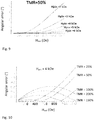
- Fig. 9 shows the angular error in the orientation of the pinned reference layer magnetization 210 as a function of the magnitude of the external magnetic field H ext for several values of the pinning field H pin (pinning strength) and for the magnetic sensor elements 20 having a TMR of 50%.
- Fig. 10 shows total angular error as a function of the magnitude of the external magnetic field H ext for several values of TMR in the magnetic sensor elements 20 and for a pinning field H pin of 4 kOe.
- the optimum can be found numerically and/or optimized by adequate designing of the magnetic sensor element 20.
- the strength of the antiferromagnetic coupling (the magnitude of the pinning field H pin ) should be high enough to keep the reference layer magnetization 210 rigid when submitted to the external magnetic field H ext .
- Fig. 11 is a partial view of the magnetic sensor element 20 according to yet another embodiment, showing the ferromagnetic pinned layer 21, the tunnel magnetoresistance barrier layer 22 and the sensing layer 23.
- the pinned layer 21 comprises a synthetic antiferromagnet (SAF) structure, i.e., a magnetic multilayer comprising comprises ferromagnetic pinned sublayers separated by non-magnetic sublayers.
- SAF synthetic antiferromagnet
- the magnetic sensor element 20 is represented comprising three ferromagnetic pinned sublayers 211 separated by two non-magnetic sublayer 212, however the magnetic sensor element 20 can have at least two ferromagnetic pinned sublayers 211 separated by and non-magnetic sublayer 212.
- the ferromagnetic layer farthest from the tunnel barrier layer 22 is pinned by an antiferromagnet 213 while the other ferromagnetic layers are coupled to the neighbouring ferromagnetic layers by an RKKY coupling mechanism through the non-magnetic layers separating them.
- the RKKY coupling is essentially antiferromagnetic.
- Fig. 12 shows the dependence of angular error ⁇ H on the external magnetic field H ext for different TMR magnitudes for the magnetic sensor element 20 in the configuration of Fig. 11 .
- calculations were performed assuming an exchange pinning of 0.66 erg/cm 2 and the RKKY coupling of -0.66 erg/cm 2 for the ferromagnetic layers farthest from the tunnel barrier layer 22 (in the bottom part of the stack).
- the SAF configuration of the pinned layer 21 can provide the same improved compensation effect of the angular error as for the configuration shown in Fig. 8 .
- the improved compensation effect can be obtained for the RKKY exchange coupling being antiferromagnetic and having an absolute magnitude of 0.4 erg/cm 2 or greater.
Landscapes
- Physics & Mathematics (AREA)
- Condensed Matter Physics & Semiconductors (AREA)
- General Physics & Mathematics (AREA)
- Measuring Magnetic Variables (AREA)
- Hall/Mr Elements (AREA)
Abstract
Description
- The disclosure relates to a magnetic angular sensor element and to a magnetic angular sensor device comprising a plurality of the magnetic angular sensor element for detecting a magnetic field angle over a 360° range of measurement of a plane.
- Magnetic tunnel junction (MTJ) based magnetic angular sensors provide a high sensitivity, wide-range of their output resistance, better integration into CMOS process and many other attractable features compared to the competing technologies existing on the market.
- Such magnetic angular sensors require a specific MTJ typically comprising two magnetically different ferromagnetic layers separated by a dielectric tunneling barrier. One of the ferromagnetic layers (sensing layer) is magnetically soft and is easily aligned by an external magnetic field, the other one is magnetically rigid (reference layer) with a pinned direction of its magnetization.
- Tunnel magnetoresistance (TMR) effect is employed to sense the relative angle between the magnetization of the sensing layer and the magnetization of the reference layer, and thus to measure a direction of an external magnetic field. Change of the relative angle between the sensing layer and the reference layer magnetization can be determined by measuring a change of the electrical conductivity through the MTJ stack. The conductivity of a MTJ stack follows a cosine function of the relative angle between net magnetization direction in the sensing and reference layers. For 2D magnetic field sensing, magnetization of the reference layer usually lies in-plane (in the plane of the reference layer), while magnetic state of the sensing layer can be different. Due to this functional dependence, two MTJ stacks with 90° shifted pinning direction of their reference layers are enough to make a 2D magnetic field angle sensor.
-
Fig. 1 shows a single-branch sensing circuit 10 comprising amagnetic sensor element 20. Themagnetic sensor element 20 can comprise one or several electrically connected MTJ pillars fabricated from an MTJ stack, all having the same pinning direction of reference layer. Each MTJ stack comprises (not shown) a tunnel barrier layer sandwiched between a reference layer, a sensing layer. When an externalmagnetic field 60 is applied, thesensing layer magnetization 230 is oriented in the direction of the externalmagnetic field 60. The orientation of thereference layer magnetization 210 remains unchanged. The direction of the externalmagnetic field 60 can thus be measured by passing a sensing current in themagnetic sensor element 20 and measuring voltage difference (Vout - Vin) being proportional to the resistance R of themagnetic sensor element 20. - Ideally, the
reference layer magnetization 210 should be insensible to the external magnetic field within the working range of the sensor while thesensing layer magnetization 230 should be perfectly soft and thus should be magnetized exactly along the direction of the externalmagnetic field 60. - Practically however, the sensing layer magnetization has a finite magnetic anisotropy and the sensing layer magnetization can be subjected to finite stray field from the reference layer. This causes angular errors in the alignment of the sensing layer magnetization in the external
magnetic field 60 and thus, in the expected resistance R of the magnetic sensor element for a given angle ofmagnetic field 60. These angular errors limit operational margin of the sensor at low magnitudes of the external magnetic field, since the angular error increases when lowering the magnitude of the externalmagnetic field 60. - Moreover, the reference layer has finite magnetic stiffness and therefore its magnetization can be deflected (even only slightly) by the external magnetic field. This also produces angular errors in the alignment of the reference layer magnetization. These angular errors increase with the magnitude of the external magnetic field and therefore limit the high-field operation margin of the magnetic sensor element.
-
Fig. 2 reports the variation of the total angular error AET as a function of the magnitude of an external magnetic field Hext. The total angular error AET corresponds to a difference between the measured relative angle between the direction of the sensing layer magnetization and reference layer magnetization when an external magnetic field is applied and an "ideal" relative angle, i.e., when the sensing layer magnetization is completely aligned in the direction of the external magnetic field, and when the reference layer magnetization is not deflected by the external magnetic field. The variation of the total angular error AET corresponds to the sum of the angular error AEs in sensing layer orientation due to anisotropy in sensing layer, bias field etc., and angular error AER in reference layer magnetization orientation due to finite reference layer pinning strength. -
Fig. 3 shows analternative sensing circuit 30 comprising twomagnetic sensor elements 20 arranged in a half-bridge configuration. The half-bridge circuit 30 produces an output voltage Vout that is a fraction of its input voltage Vin. One of the twomagnetic sensor elements 20 has areference layer magnetization 210 that is pinned in a direction opposed thereference layer magnetization 210 of the othermagnetic sensor element 20. - As discussed above, the
reference layer magnetization 210 in the twomagnetic sensor elements 20 can be deflected towards the direction of an applied external magnetic field 60 (shown by the curved arrow inFig. 3 ). The deflection causes thereference layer magnetization 210 to be more parallel to thesensing layer magnetization 230 and tends to decrease the resistance in each of the twomagnetic sensor elements 20. However, the half-bridge sensing circuit 30 configuration results in a lower relative change in the voltage divider ratio Vout/Vin than the relative change of resistance in eachmagnetic sensor elements 20 measured separately. This is achieved due to the opposed direction of the pinnedreference layer magnetization 210 in the twomagnetic sensor elements 20. The half-bridge sensing circuit 30 ofFig. 3 allows for partial compensation of the angular error AER (thus of the total angular error AET) due to the deflection of thereference layer magnetization 210. -
Fig. 4 compares the variation of the total angular error AET as a function of the magnitude Hext of an external magnetic field, calculated for the single-branch sensing circuit 10 ofFig. 1 (line with triangles) and for the half-bridge sensing circuit 30 ofFig. 3 (single line). The calculations were made for different magnitudes of anisotropy strength in sensing layer (Hua), and for different pinning field strength (Hud) in the reference layer. The half-bridge sensing circuit 30 shows lower total angular error AET compared to the single-branch sensing circuit 10 ofFig. 1 . - Our study has shown that compensation of finite reference layer pinning strength is not fully achieved by using a half bridge circuit configuration due to simultaneous action of two factors.
- A first factor concerns the in-plane transversal (a direction perpendicular to the pinning field direction of the reference layer) magnetic susceptibility χR of the reference layer that is asymmetrical with respect to the external magnetic field sign for a given magnetic field angle..
-
Figs. 5a and 5b represent the external magnetic field Hext having a longitudinal component Hlong corresponding to a projection along the direction of the pinning field Hpin (of the antiferromagnetic layer exchange coupling the reference layer) and a transversal component Htrans corresponding to a projection along a direction perpendicular to the one of the pinning field Hpin. Transversal susceptibility χR can be defined as Htrans/Heff, where Heff = Hpin + Hlong. Considering the case where Hpin is always greater in magnitude than Hext magnitude, Heff will be always larger when directions of Hpin and Hlong are parallel and smaller when those are anti-parallel. Consequently, the susceptibility χR will be smaller in the first case and larger in the second case. -
Fig. 6 reports the deviation in degree of thereference layer magnetization 210 relative to its pinned orientation, as a function of the orientation of the external magnetic field Hext for the half-bridge sensing circuit 30 ofFig. 3 . The deviation is shown for themagnetic sensor element 20 of the top branch (curve A) where the pinned reference layer magnetization 210 (pinning field Hpin) is parallel to the longitudinal component Hlong (Fig. 5a ) and for themagnetic sensor element 20 of the bottom branch (curve B) where the pinned reference layer magnetization 210 (pinning field Hpin) is antiparallel to the longitudinal component Hong (Fig. 5b ). The orientation angle of the external magnetic field Hext shown inFig. 5 is indicated by the dotted line inFig. 6 . It corresponds to a deviation of thereference layer magnetization 210 of about 5° for themagnetic sensor element 20 of the top branch (curve A) and about 7° for themagnetic sensor element 20 of the bottom branch (curve B). - The reference magnetic susceptibility χR (i.e. level of the reference layer angular deviation) decreases when the external magnetic field Hext has a longitudinal component Hlong which is parallel to the pinning field Hpin of the antiferromagnetic layer (see
Fig. 5a ). This is due to the pinning field Hpin and the longitudinal component Hlong of the external field Hext adding up, making the reference layer magnetization more difficult to deviate towards the transversal component Htrans of the external field Hext. Conversely, the reference magnetic susceptibility χR increases when the external magnetic field Hext has a longitudinal component Hlong which is antiparallel to the pinning field Hpin of the antiferromagnetic layer (seeFig. 5b ). In this configuration, the longitudinal component Hlong of the external field Hext is subtracted from the pinning field Hpin, thus reducing the stiffness of the reference layer magnetization. - Therefore, the first factor is related to unequal deviations of
reference layers 210 directions in presence of externalmagnetic field 60. Onesensing element 20 of those two shown onfig. 3 , for which the longitudinal component of the externalmagnetic field 60 is more antiparallel to the pinning direction of itsreference layer 210, have stronger deviation than the other one. - A second factor concerns the relative change of resistance in the two
magnetic sensor elements 20. In each branch (each magnetic sensor element 20), a change of the resistance per one degree is dependent on the relative angle θ between the sensing layer and the reference layer (seeFig. 3 ). The higher the angle θ, the higher the relative change per degree. This is because not the resistance but the conductance of a branch is proportional to cosine of the angle θ between the sensing layer and the reference layer. The rate of change in resistance R with the angle θ is given by equation 1:
-
Fig. 7 reports the variation of the resistance with the angle ∂R/∂θ as a function of the orientation of thereference layer magnetization 210 relative to thesensing layer magnetization 230 for different TMR magnitudes (defined as 100%*(Rap-Rp)/Rp, where Rap is electrical resistance ofsensing element 20 whensensing layer 230 is antiparallel toreference layer 210, and Rp is the corresponding resistance for their parallel configuration), in the half-bridge sensing circuit 30 ofFig. 3 . Namely the variation of the resistance is reported for a resistance Rap of thesensing elements 20 forming ahalf bridge circuit 30 ofFig. 3 and having values of 1.1 kΩ, 1.3 kΩ and 2.0 kΩ. - An angle θ decreasing below 90° corresponds to the
sensing layer magnetization 230 approaching an orientation parallel to thereference layer magnetization 210. An angle θ increasing above 90° corresponds to the sensing layer magnetization approaching an orientation antiparallel to thereference layer magnetization 210. The effect of the relative change of resistance R in the two branches is more important when themagnetic sensor element 20 has a higher TMR. -
Fig. 7 further shows that, for a given orientation of the external magnetic field Hext, themagnetic sensor element 20 where thesensing layer magnetization 230 is oriented closer to an antiparallel orientation to thereference layer magnetization 210 will have higher deviation of thereference layer magnetization 210 and, at the same time, higher change of the resistance per one degree of angular deviation. Thus, the higher the TMR and the softer the reference layer, the smaller the compensational effect of half-bridge circuit configuration and the higher the angular errors at high external magnetic fields. - The present disclosure concerns a magnetic angular sensor element destined to sense an external magnetic field, comprising a magnetic tunnel junction containing a ferromagnetic pinned layer having a pinned magnetization, a ferromagnetic sensing layer, and a tunnel magnetoresistance spacer layer; the ferromagnetic sensing layer comprising a first sensing layer being in direct contact with the spacer layer and having a first sensing magnetization, a second sensing layer having a second sense magnetization, and a metallic spacer between the first sensing layer and the second sensing layer; wherein the metallic spacer is configured to provide an antiferromagnetic coupling between the first sensing magnetization and the second sensing magnetization such that the first sensing magnetization is oriented substantially antiparallel to the second sensing magnetization; the second sensing magnetization being larger than the first sensing magnetization, such that the second sensing magnetization is oriented in accordance with the direction of the external magnetic field.
- The present disclosure further concerns a magnetic angular sensor device comprising a plurality of the magnetic sensor element; wherein the magnetic sensor elements are arranged in a half-bridge or full bridge configuration.
- The magnetic angular sensor element disclosed herein in the half-bridge circuit (or a full-bridge circuit) improved compensation of the angular error AET compared to known arrangement of the magnetic angular sensor element, not only at low magnitudes of the external
magnetic field 60 but also at high magnitudes of the externalmagnetic field 60 - The invention will be better understood with the aid of the description of an embodiment given by way of example and illustrated by the figures, in which:
-
Fig. 1 shows a single-branch sensing circuit comprising a plurality of electrically connected MTJ pillars fabricated from an MTJ film stack. All MTJ pillars share the same pinning direction of their reference layer. -
Fig. 2 reports the variation of the total angular error as a function of the magnitude of an external magnetic field; -
Fig. 3 shows a sensing circuit comprising two MTJ sensing circuits arranged in a half-bridge configuration; -
Fig. 4 compares the variation of the total angular error as a function of the magnitude of an external magnetic field, calculated for the single-branch (SB) sensing circuit ofFig. 1 and for the half-bridge (HB) sensing circuit ofFig. 3 ; -
Figs. 5a and 5b represent a longitudinal component and a transversal component of the external magnetic field; -
Fig. 6 reports the deviation of the reference layer magnetization relative to its pinned orientation as a function of the orientation of the external magnetic field for the half-bridge sensing circuit ofFig. 3 ; -
Fig. 7 reports the variation of the derivative of the resistance with the angle as a function of the orientation of the reference layer magnetization relative to the sensing layer magnetization for different TMR; -
Fig. 8 shows a magnetic angular sensor element, according to an embodiment; -
Fig. 9 shows total angular error as a function of the magnitude of the external magnetic field for several values of the pinning field strength; -
Fig. 10 shows total angular error as a function of the magnitude of the external magnetic field for several values of TMR in MTJ stack. -
Fig. 8 shows a magneticangular sensor element 20 destined to sense an external magnetic field (Hext) 60, according to an embodiment. Themagnetic sensor element 20 comprises a magnetic tunnel junction containing a ferromagnetic pinnedlayer 21 having a pinnedmagnetization 210, aferromagnetic sensing layer 23, and a tunnelmagnetoresistance barrier layer 22, between the ferromagnetic pinnedlayer 21 and theferromagnetic sensing layer 23. Theferromagnetic sensing layer 23 comprises afirst sensing layer 23a being in direct contact with thebarrier layer 22 and having afirst sensing magnetization 230a, asecond sensing layer 23b having asecond sense magnetization 230b, and ametallic spacer 24 between thefirst sensing layer 23a and thesecond sensing layer 23b. - The
metallic spacer 24 is configured to provide an antiferromagnetic coupling between thefirst sensing magnetization 230a and thesecond sensing magnetization 230b such that thefirst sensing magnetization 230a is oriented substantially antiparallel to thesecond sensing magnetization 230b. - The
second sensing magnetization 230b is larger than thefirst sensing magnetization 230a, such that thesecond sensing magnetization 230b is oriented in accordance with the direction of the externalmagnetic field 60. - The present invention further pertains to a magnetic angular sensor device comprising a plurality of the
magnetic sensor element 20. - In a preferred embodiment, the
magnetic sensor elements 20 are arranged in a half-bridge circuit 30, as represented inFig. 3 . Themagnetic sensor elements 20 can also be arranged in a full bridge configuration. - When the external magnetic field Hext is applied in a direction that is close to an antiparallel orientation with respect to the pinned direction of the
reference layer magnetization 210, a higher deviation of thereference layer magnetization 210 occurs (first factor). However, the firstsensing layer magnetization 230a is oriented close to a parallel orientation with respect to the pinned direction of thereference layer magnetization 210, reducing the resistance variation per one degree of the reference layer deviation (second factor). The deviation of thereference layer magnetization 210 is thus at least partially compensated by a decrease of the angular variation of the resistance R. - Using the magnetic
angular sensor element 20 in the half-bridge circuit 30 (or a full-bridge circuit) improves the compensation of the angular error AET compared to known arrangement of the magnetic angular sensor element, not only at low magnitudes of the externalmagnetic field 60 but also at high magnitudes of the externalmagnetic field 60. - In an embodiment, the
second sensing layer 23b comprises a plurality ofsecond sensing sublayers 231, eachsecond sensing sublayer 231 having asecond sensing sub-magnetization 2310 amounting to saidsecond sensing magnetization 230b. Two adjacentsecond sensing sublayers 231 are separated from by anon-magnetic layer 232 being configured to provide a magnetic coupling between the two adjacentsecond sensing sublayers 231. - In another embodiment, the
non-magnetic layer 232 is configured to provide a magnetic coupling such that thesecond sensing magnetization 230b is oriented in a direction opposed to the one of thefirst sensing magnetization 230a. - In yet another embodiment, the magnetic coupling is such that the
second sensing sub-magnetization 2310 of one of thesecond sensing sublayers 231 is oriented substantially parallel to the one of the adjacentsecond sensing sublayer 231. - In yet another embodiment, the
non-magnetic layer 232 is configured to have a strength (a minimal required strength) of the magnetic coupling such that there is no reversal of thesecond sensing sub-magnetization 2310 within thesecond sensing sublayer 231 for an amplitude of the externalmagnetic field 60 up to 1200 Oe. - In yet another embodiment, the antiferromagnetic coupling of the
metallic spacer 24 is a RKKY coupling having an exchange coupling of 0.3 erg/cm2 or greater. - In yet another embodiment, the
first sensing magnetization 230a has a thickness of 1.5 nm or greater. - A RKKY coupling having an exchange coupling of 0.3 erg/cm2 or greater is enough to stabilize the
first sensing layer 23a andsecond sensing layer 23b in the antiferromagnetic configuration for an external magnetic field Hext that is below 1200 Oe. - I yet another embodiment, the layers order as shown in
Fig. 8 is inverted. Such configuration corresponds to a so-called top-pinned MTJ stack. - For any given TMR magnitude, increasing the pinning strength of the
reference layer 21 reduces the asymmetry in the reference magnetic susceptibility χR of thereference layer 21 in themagnetic sensor element 20 in the top branch and bottom branch of the half-bridge circuit 30. Increasing the pinning strength of thereference layer 21 thus diminishes the impact of the effect of the second factor as defined above. -
Fig. 9 shows the angular error in the orientation of the pinnedreference layer magnetization 210 as a function of the magnitude of the external magnetic field Hext for several values of the pinning field Hpin (pinning strength) and for themagnetic sensor elements 20 having a TMR of 50%. - For any given reference layer pinning field Hpin, there is an optimal TMR value which provides optimal compensation at a desired magnitude of the external magnetic field Hext.
Fig. 10 shows total angular error as a function of the magnitude of the external magnetic field Hext for several values of TMR in themagnetic sensor elements 20 and for a pinning field Hpin of 4 kOe. The optimum (minimum angular error) can be found numerically and/or optimized by adequate designing of themagnetic sensor element 20. - The strength of the antiferromagnetic coupling (the magnitude of the pinning field Hpin) should be high enough to keep the
reference layer magnetization 210 rigid when submitted to the external magnetic field Hext. -
Fig. 11 is a partial view of themagnetic sensor element 20 according to yet another embodiment, showing the ferromagnetic pinnedlayer 21, the tunnelmagnetoresistance barrier layer 22 and thesensing layer 23. The pinnedlayer 21 comprises a synthetic antiferromagnet (SAF) structure, i.e., a magnetic multilayer comprising comprises ferromagnetic pinned sublayers separated by non-magnetic sublayers. InFig. 11 themagnetic sensor element 20 is represented comprising three ferromagnetic pinnedsublayers 211 separated by twonon-magnetic sublayer 212, however themagnetic sensor element 20 can have at least two ferromagnetic pinnedsublayers 211 separated by andnon-magnetic sublayer 212. The ferromagnetic layer farthest from thetunnel barrier layer 22 is pinned by anantiferromagnet 213 while the other ferromagnetic layers are coupled to the neighbouring ferromagnetic layers by an RKKY coupling mechanism through the non-magnetic layers separating them. Here, the RKKY coupling is essentially antiferromagnetic. -
Fig. 12 shows the dependence of angular error ΔϕH on the external magnetic field Hext for different TMR magnitudes for themagnetic sensor element 20 in the configuration ofFig. 11 . Here, calculations were performed assuming an exchange pinning of 0.66 erg/cm2 and the RKKY coupling of -0.66 erg/cm2 for the ferromagnetic layers farthest from the tunnel barrier layer 22 (in the bottom part of the stack). As can be seen fromFig. 12 , the SAF configuration of the pinnedlayer 21 can provide the same improved compensation effect of the angular error as for the configuration shown inFig. 8 . In fact, the improved compensation effect can be obtained for the RKKY exchange coupling being antiferromagnetic and having an absolute magnitude of 0.4 erg/cm2 or greater. -
- 10
- magnetic angular sensor device, sensing circuit
- 20
- magnetic angular sensor element, MTJ
- 21
- ferromagnetic pinned layer
- 210
- reference layer magnetization, pinned magnetization
- 211
- ferromagnetic pinned sublayer
- 212
- non-magnetic sublayer
- 213
- antiferromagnet
- 22
- barrier layer
- 23
- ferromagnetic sensing layer
- 23a
- first sensing layer
- 230
- sensing layer magnetization
- 230a
- first sensing magnetization
- 23b
- second sensing layer
- 230b
- second sensing magnetization
- 24
- metallic spacer
- 231
- second sensing sublayer
- 2310
- second sensing sub-magnetization
- 232
- non-magnetic layer
- 30
- sensing circuit
- 60
- external magnetic field
- AET
- total angular error
- AER
- angular error in reference layer orientation
- AES
- angular error in sensing layer orientation
- Hext
- magnitude of an external magnetic field
- Hlong
- longitudinal component
- Hpin
- pinning field
- Htrans
- transversal component
- R
- resistance
- Rap
- resistance when the sensing and reference layer magnetization are antiparallel
- Vin
- inutput voltage
- Vout
- output voltage
- θ
- angle
- χR
- magnetic susceptibility of the reference layer
- χtrans
- transversal magnetic susceptibility
Claims (9)
- Magnetic angular sensor element (20) destined to sense an external magnetic field (60), comprising:a magnetic tunnel junction (2) containing a ferromagnetic pinned layer (21) having a pinned magnetization (210), a ferromagnetic sensing layer (23), and a tunnel magnetoresistance barrier layer (22), between the ferromagnetic pinned layer (21) and the ferromagnetic sensing layer (23);characterized in thatthe ferromagnetic sensing layer (23) comprises a first sensing layer (23a) being in direct contact with the barrier layer (22) and having a first sensing magnetization (230a), a second sensing layer (23b) having a second sense magnetization (230b), and a metallic spacer (24) between the first sensing layer (23a) and the second sensing layer (23b);wherein the metallic spacer (24) is configured to provide an antiferromagnetic coupling between the first sensing magnetization (230a) and the second sensing magnetization (230b) such that the first sensing magnetization (230a) is oriented substantially antiparallel to the second sensing magnetization (230b); andin that the second sensing magnetization (230b) is larger than the first sensing magnetization (230a), such that the second sensing magnetization (230b) is oriented in accordance with the direction of the external magnetic field (60).
- The magnetic sensor element (20) according to claim 1,
wherein the second sensing layer (23b) comprises a plurality of second sensing sublayers (231), each second sensing sublayer (231) having a second sensing sub-magnetization (2310) amounting to said second sensing magnetization (230b); and
wherein two adjacent second sensing sublayers (231) are separated from by a non-magnetic layer (232) being configured to provide a magnetic coupling between the two adjacent second sensing sublayers (231). - The magnetic sensor element (20) according to claim 1 or 2,
wherein the non-magnetic layer (232) is configured to provide a magnetic coupling such that the second sensing magnetization (230b) is oriented in a direction opposed to the one of the first sensing magnetization (230a). - The magnetic sensor element (20) according to claim 2 or 3,
wherein the magnetic coupling is such that the second sensing sub-magnetization (2310) of one of the second sensing sublayers (231) is oriented substantially parallel to the one of the adjacent second sensing sublayer (231). - The magnetic sensor element (20) according to any one of claims 2 to 4,
wherein the non-magnetic layer (232) is configured to have a strength of the magnetic coupling of 1 erg/cm2 or greater such that there is no reversal of the second sensing sub-magnetization (2310) within the second sensing sublayer (231) for an amplitude of the external magnetic field (60) up to 1200 Oe. - The magnetic sensor element (20) according to any one of claims 1 to 5,
wherein the antiferromagnetic coupling of the metallic spacer (24) is a RKKY coupling having an exchange coupling of 0.3 erg/cm2 or greater. - The magnetic sensor element (20) according to any one of claims 1 to 6,
the pinned layer (21) comprises ferromagnetic layers separated by and non-magnetic layers where the ferromagnetic layers farthest from the tunnel barrier layer (22) are pinned by an antiferromagnet while the other ferromagnetic layers are coupled to the neighbouring ferromagnetic layers by an RKKY coupling mechanism through the non-magnetic layers separating them, wherein the RKKY exchange coupling is antiferromagnetic and has an absolute magnitude of 0.4 erg/cm2 or greater. - The magnetic sensor element (20) according to claim 6 or 7,
wherein the first sensing magnetization (230a) has a thickness of 1.5 nm or greater. - A magnetic angular sensor device (30) comprising a plurality of the magnetic sensor element (20) according to any one of claims 1 to 8;
wherein the magnetic sensor elements (20) are arranged in a half-bridge or full bridge configuration.
Priority Applications (5)
| Application Number | Priority Date | Filing Date | Title |
|---|---|---|---|
| EP20315252.5A EP3913386B1 (en) | 2020-05-20 | 2020-05-20 | Magnetic sensor element and device having improved accuracy under high magnetic fields |
| KR1020227039540A KR102844286B1 (en) | 2020-05-20 | 2021-05-10 | Magnetic sensor elements and devices with improved accuracy under high magnetic fields |
| JP2022568458A JP2023526003A (en) | 2020-05-20 | 2021-05-10 | Magnetic sensor element and device with improved accuracy at high magnetic fields |
| PCT/IB2021/053951 WO2021234504A1 (en) | 2020-05-20 | 2021-05-10 | Magnetic sensor element and device having improved accuracy under high magnetic fields |
| US17/998,984 US12228620B2 (en) | 2020-05-20 | 2021-05-10 | Magnetic sensor element and device having improved accuracy under high magnetic fields |
Applications Claiming Priority (1)
| Application Number | Priority Date | Filing Date | Title |
|---|---|---|---|
| EP20315252.5A EP3913386B1 (en) | 2020-05-20 | 2020-05-20 | Magnetic sensor element and device having improved accuracy under high magnetic fields |
Publications (2)
| Publication Number | Publication Date |
|---|---|
| EP3913386A1 true EP3913386A1 (en) | 2021-11-24 |
| EP3913386B1 EP3913386B1 (en) | 2026-02-11 |
Family
ID=71452171
Family Applications (1)
| Application Number | Title | Priority Date | Filing Date |
|---|---|---|---|
| EP20315252.5A Active EP3913386B1 (en) | 2020-05-20 | 2020-05-20 | Magnetic sensor element and device having improved accuracy under high magnetic fields |
Country Status (5)
| Country | Link |
|---|---|
| US (1) | US12228620B2 (en) |
| EP (1) | EP3913386B1 (en) |
| JP (1) | JP2023526003A (en) |
| KR (1) | KR102844286B1 (en) |
| WO (1) | WO2021234504A1 (en) |
Families Citing this family (1)
| Publication number | Priority date | Publication date | Assignee | Title |
|---|---|---|---|---|
| US12310101B2 (en) * | 2020-12-23 | 2025-05-20 | Intel Corporation | Gate dielectrics for complementary metal oxide semiconductors transistors and methods of fabrication |
Citations (2)
| Publication number | Priority date | Publication date | Assignee | Title |
|---|---|---|---|---|
| JP2011027633A (en) * | 2009-07-28 | 2011-02-10 | Tdk Corp | Magnetic sensor and manufacturing method thereof |
| US20190051822A1 (en) * | 2017-08-10 | 2019-02-14 | Commissariat A L'energie Atomique Et Aux Energies Alternatives | Synthetic antiferromagnetic layer, magnetic tunnel junction and spintronic device using said synthetic antiferromagnetic layer |
Family Cites Families (11)
| Publication number | Priority date | Publication date | Assignee | Title |
|---|---|---|---|---|
| JP2008010590A (en) * | 2006-06-28 | 2008-01-17 | Toshiba Corp | Magnetoresistive element and magnetic memory |
| JP2008166524A (en) * | 2006-12-28 | 2008-07-17 | Alps Electric Co Ltd | Tunnel type magnetic sensor |
| WO2008102499A1 (en) * | 2007-02-23 | 2008-08-28 | Nec Corporation | Magnetic substance device, and magnetic random access memory |
| KR101224100B1 (en) * | 2009-09-10 | 2013-01-18 | 대상 주식회사 | Process for producing curry in form of granules having high dispersibility |
| JP2011064653A (en) * | 2009-09-18 | 2011-03-31 | Tdk Corp | Magnetic sensor and method of manufacturing the same |
| US9368176B2 (en) | 2012-04-20 | 2016-06-14 | Alexander Mikhailovich Shukh | Scalable magnetoresistive element |
| TWI468715B (en) * | 2012-10-22 | 2015-01-11 | 財團法人工業技術研究院 | Magnetic field sensor for sensing an external magnetic field |
| US9252710B2 (en) * | 2012-11-27 | 2016-02-02 | Headway Technologies, Inc. | Free layer with out-of-plane anisotropy for magnetic device applications |
| JP2015213125A (en) * | 2014-05-02 | 2015-11-26 | 日本放送協会 | Spin injection magnetization reversal element |
| JP6121943B2 (en) * | 2014-05-16 | 2017-04-26 | 株式会社東芝 | Magnetic head and magnetic recording / reproducing apparatus |
| US10620279B2 (en) * | 2017-05-19 | 2020-04-14 | Allegro Microsystems, Llc | Magnetoresistance element with increased operational range |
-
2020
- 2020-05-20 EP EP20315252.5A patent/EP3913386B1/en active Active
-
2021
- 2021-05-10 KR KR1020227039540A patent/KR102844286B1/en active Active
- 2021-05-10 WO PCT/IB2021/053951 patent/WO2021234504A1/en not_active Ceased
- 2021-05-10 US US17/998,984 patent/US12228620B2/en active Active
- 2021-05-10 JP JP2022568458A patent/JP2023526003A/en active Pending
Patent Citations (2)
| Publication number | Priority date | Publication date | Assignee | Title |
|---|---|---|---|---|
| JP2011027633A (en) * | 2009-07-28 | 2011-02-10 | Tdk Corp | Magnetic sensor and manufacturing method thereof |
| US20190051822A1 (en) * | 2017-08-10 | 2019-02-14 | Commissariat A L'energie Atomique Et Aux Energies Alternatives | Synthetic antiferromagnetic layer, magnetic tunnel junction and spintronic device using said synthetic antiferromagnetic layer |
Also Published As
| Publication number | Publication date |
|---|---|
| US12228620B2 (en) | 2025-02-18 |
| US20230213597A1 (en) | 2023-07-06 |
| JP2023526003A (en) | 2023-06-20 |
| KR102844286B1 (en) | 2025-08-08 |
| EP3913386B1 (en) | 2026-02-11 |
| KR20230013027A (en) | 2023-01-26 |
| WO2021234504A1 (en) | 2021-11-25 |
Similar Documents
| Publication | Publication Date | Title |
|---|---|---|
| US10935612B2 (en) | Current sensor having multiple sensitivity ranges | |
| US7394240B2 (en) | Current sensor | |
| US11860250B2 (en) | Magnetic angular sensor device for sensing high magnetic fields with low angular error | |
| US7737678B2 (en) | Magnetic sensor and current sensor | |
| US7723983B2 (en) | Magnetic sensor and current sensor | |
| US12265139B2 (en) | Magneto-resistive element and magnetic sensor | |
| US9465056B2 (en) | Current sensor with temperature-compensated magnetic tunnel junction bridge | |
| US7394247B1 (en) | Magnetic field angle sensor with GMR or MTJ elements | |
| US7750620B2 (en) | MTJ sensor based method to measure an electric current | |
| JP6886222B2 (en) | Magnetic sensor | |
| EP3531153B1 (en) | Spin valve with bias alignment | |
| US10557726B2 (en) | Systems and methods for reducing angle error for magnetic field angle sensors | |
| US12228620B2 (en) | Magnetic sensor element and device having improved accuracy under high magnetic fields | |
| WO2015125699A1 (en) | Magnetic sensor | |
| US11747411B2 (en) | Magnetoresistive-based sensing circuit for two-dimensional sensing of high magnetic fields |
Legal Events
| Date | Code | Title | Description |
|---|---|---|---|
| PUAI | Public reference made under article 153(3) epc to a published international application that has entered the european phase |
Free format text: ORIGINAL CODE: 0009012 |
|
| STAA | Information on the status of an ep patent application or granted ep patent |
Free format text: STATUS: THE APPLICATION HAS BEEN PUBLISHED |
|
| AK | Designated contracting states |
Kind code of ref document: A1 Designated state(s): AL AT BE BG CH CY CZ DE DK EE ES FI FR GB GR HR HU IE IS IT LI LT LU LV MC MK MT NL NO PL PT RO RS SE SI SK SM TR |
|
| B565 | Issuance of search results under rule 164(2) epc |
Effective date: 20201118 |
|
| STAA | Information on the status of an ep patent application or granted ep patent |
Free format text: STATUS: REQUEST FOR EXAMINATION WAS MADE |
|
| 17P | Request for examination filed |
Effective date: 20220411 |
|
| RBV | Designated contracting states (corrected) |
Designated state(s): AL AT BE BG CH CY CZ DE DK EE ES FI FR GB GR HR HU IE IS IT LI LT LU LV MC MK MT NL NO PL PT RO RS SE SI SK SM TR |
|
| RAP3 | Party data changed (applicant data changed or rights of an application transferred) |
Owner name: CROCUS TECHNOLOGY SA |
|
| RAP1 | Party data changed (applicant data changed or rights of an application transferred) |
Owner name: ALLEGRO MICROSYSTEMS, LLC |
|
| GRAP | Despatch of communication of intention to grant a patent |
Free format text: ORIGINAL CODE: EPIDOSNIGR1 |
|
| STAA | Information on the status of an ep patent application or granted ep patent |
Free format text: STATUS: GRANT OF PATENT IS INTENDED |
|
| RIC1 | Information provided on ipc code assigned before grant |
Ipc: G01R 33/09 20060101AFI20251029BHEP Ipc: G01R 33/00 20060101ALI20251029BHEP |
|
| INTG | Intention to grant announced |
Effective date: 20251125 |
|
| GRAS | Grant fee paid |
Free format text: ORIGINAL CODE: EPIDOSNIGR3 |
|
| GRAA | (expected) grant |
Free format text: ORIGINAL CODE: 0009210 |
|
| STAA | Information on the status of an ep patent application or granted ep patent |
Free format text: STATUS: THE PATENT HAS BEEN GRANTED |
|
| AK | Designated contracting states |
Kind code of ref document: B1 Designated state(s): AL AT BE BG CH CY CZ DE DK EE ES FI FR GB GR HR HU IE IS IT LI LT LU LV MC MK MT NL NO PL PT RO RS SE SI SK SM TR |
|
| REG | Reference to a national code |
Ref country code: CH Ref legal event code: F10 Free format text: ST27 STATUS EVENT CODE: U-0-0-F10-F00 (AS PROVIDED BY THE NATIONAL OFFICE) Effective date: 20260211 Ref country code: GB Ref legal event code: FG4D |
|
| REG | Reference to a national code |
Ref country code: DE Ref legal event code: R096 Ref document number: 602020066653 Country of ref document: DE |
|
| REG | Reference to a national code |
Ref country code: IE Ref legal event code: FG4D |
|
| REG | Reference to a national code |
Ref country code: NL Ref legal event code: MP Effective date: 20260211 |
|
| PG25 | Lapsed in a contracting state [announced via postgrant information from national office to epo] |
Ref country code: RS Free format text: LAPSE BECAUSE OF FAILURE TO SUBMIT A TRANSLATION OF THE DESCRIPTION OR TO PAY THE FEE WITHIN THE PRESCRIBED TIME-LIMIT Effective date: 20260511 |
|
| PG25 | Lapsed in a contracting state [announced via postgrant information from national office to epo] |
Ref country code: ES Free format text: LAPSE BECAUSE OF FAILURE TO SUBMIT A TRANSLATION OF THE DESCRIPTION OR TO PAY THE FEE WITHIN THE PRESCRIBED TIME-LIMIT Effective date: 20260211 |
|
| PG25 | Lapsed in a contracting state [announced via postgrant information from national office to epo] |
Ref country code: PL Free format text: LAPSE BECAUSE OF FAILURE TO SUBMIT A TRANSLATION OF THE DESCRIPTION OR TO PAY THE FEE WITHIN THE PRESCRIBED TIME-LIMIT Effective date: 20260211 |
|
| PG25 | Lapsed in a contracting state [announced via postgrant information from national office to epo] |
Ref country code: GR Free format text: LAPSE BECAUSE OF FAILURE TO SUBMIT A TRANSLATION OF THE DESCRIPTION OR TO PAY THE FEE WITHIN THE PRESCRIBED TIME-LIMIT Effective date: 20260512 |
|
| REG | Reference to a national code |
Ref country code: LT Ref legal event code: MG9D |
|
| PG25 | Lapsed in a contracting state [announced via postgrant information from national office to epo] |
Ref country code: LT Free format text: LAPSE BECAUSE OF FAILURE TO SUBMIT A TRANSLATION OF THE DESCRIPTION OR TO PAY THE FEE WITHIN THE PRESCRIBED TIME-LIMIT Effective date: 20260211 |
|
| PGFP | Annual fee paid to national office [announced via postgrant information from national office to epo] |
Ref country code: DE Payment date: 20260324 Year of fee payment: 7 |
|
| PG25 | Lapsed in a contracting state [announced via postgrant information from national office to epo] |
Ref country code: NO Free format text: LAPSE BECAUSE OF FAILURE TO SUBMIT A TRANSLATION OF THE DESCRIPTION OR TO PAY THE FEE WITHIN THE PRESCRIBED TIME-LIMIT Effective date: 20260511 |
|
| PG25 | Lapsed in a contracting state [announced via postgrant information from national office to epo] |
Ref country code: SE Free format text: LAPSE BECAUSE OF FAILURE TO SUBMIT A TRANSLATION OF THE DESCRIPTION OR TO PAY THE FEE WITHIN THE PRESCRIBED TIME-LIMIT Effective date: 20260211 Ref country code: FI Free format text: LAPSE BECAUSE OF FAILURE TO SUBMIT A TRANSLATION OF THE DESCRIPTION OR TO PAY THE FEE WITHIN THE PRESCRIBED TIME-LIMIT Effective date: 20260211 Ref country code: AT Free format text: LAPSE BECAUSE OF FAILURE TO SUBMIT A TRANSLATION OF THE DESCRIPTION OR TO PAY THE FEE WITHIN THE PRESCRIBED TIME-LIMIT Effective date: 20260211 |
|
| REG | Reference to a national code |
Ref country code: AT Ref legal event code: MK05 Ref document number: 1886082 Country of ref document: AT Kind code of ref document: T Effective date: 20260211 |
|
| PG25 | Lapsed in a contracting state [announced via postgrant information from national office to epo] |
Ref country code: HR Free format text: LAPSE BECAUSE OF FAILURE TO SUBMIT A TRANSLATION OF THE DESCRIPTION OR TO PAY THE FEE WITHIN THE PRESCRIBED TIME-LIMIT Effective date: 20260211 |
|
| PG25 | Lapsed in a contracting state [announced via postgrant information from national office to epo] |
Ref country code: PT Free format text: LAPSE BECAUSE OF FAILURE TO SUBMIT A TRANSLATION OF THE DESCRIPTION OR TO PAY THE FEE WITHIN THE PRESCRIBED TIME-LIMIT Effective date: 20260611 Ref country code: IS Free format text: LAPSE BECAUSE OF FAILURE TO SUBMIT A TRANSLATION OF THE DESCRIPTION OR TO PAY THE FEE WITHIN THE PRESCRIBED TIME-LIMIT Effective date: 20260611 |
|
| PG25 | Lapsed in a contracting state [announced via postgrant information from national office to epo] |
Ref country code: NL Free format text: LAPSE BECAUSE OF FAILURE TO SUBMIT A TRANSLATION OF THE DESCRIPTION OR TO PAY THE FEE WITHIN THE PRESCRIBED TIME-LIMIT Effective date: 20260211 |
|
| PG25 | Lapsed in a contracting state [announced via postgrant information from national office to epo] |
Ref country code: LV Free format text: LAPSE BECAUSE OF FAILURE TO SUBMIT A TRANSLATION OF THE DESCRIPTION OR TO PAY THE FEE WITHIN THE PRESCRIBED TIME-LIMIT Effective date: 20260211 |
|
| PG25 | Lapsed in a contracting state [announced via postgrant information from national office to epo] |
Ref country code: BG Free format text: LAPSE BECAUSE OF FAILURE TO SUBMIT A TRANSLATION OF THE DESCRIPTION OR TO PAY THE FEE WITHIN THE PRESCRIBED TIME-LIMIT Effective date: 20260211 |