EP3912953A1 - Process for manufacturing a micro-electro-mechanical device, in particular a movement sensor with capacitive control/detection, and mems device - Google Patents
Process for manufacturing a micro-electro-mechanical device, in particular a movement sensor with capacitive control/detection, and mems device Download PDFInfo
- Publication number
- EP3912953A1 EP3912953A1 EP21174844.7A EP21174844A EP3912953A1 EP 3912953 A1 EP3912953 A1 EP 3912953A1 EP 21174844 A EP21174844 A EP 21174844A EP 3912953 A1 EP3912953 A1 EP 3912953A1
- Authority
- EP
- European Patent Office
- Prior art keywords
- trenches
- forming
- thickness
- structural layer
- layer
- Prior art date
- Legal status (The legal status is an assumption and is not a legal conclusion. Google has not performed a legal analysis and makes no representation as to the accuracy of the status listed.)
- Granted
Links
Images




Classifications
-
- B—PERFORMING OPERATIONS; TRANSPORTING
- B81—MICROSTRUCTURAL TECHNOLOGY
- B81B—MICROSTRUCTURAL DEVICES OR SYSTEMS, e.g. MICROMECHANICAL DEVICES
- B81B3/00—Devices comprising flexible or deformable elements, e.g. comprising elastic tongues or membranes
- B81B3/0035—Constitution or structural means for controlling the movement of the flexible or deformable elements
- B81B3/0051—For defining the movement, i.e. structures that guide or limit the movement of an element
-
- B—PERFORMING OPERATIONS; TRANSPORTING
- B81—MICROSTRUCTURAL TECHNOLOGY
- B81C—PROCESSES OR APPARATUS SPECIALLY ADAPTED FOR THE MANUFACTURE OR TREATMENT OF MICROSTRUCTURAL DEVICES OR SYSTEMS
- B81C1/00—Manufacture or treatment of devices or systems in or on a substrate
- B81C1/00015—Manufacture or treatment of devices or systems in or on a substrate for manufacturing microsystems
-
- B—PERFORMING OPERATIONS; TRANSPORTING
- B81—MICROSTRUCTURAL TECHNOLOGY
- B81B—MICROSTRUCTURAL DEVICES OR SYSTEMS, e.g. MICROMECHANICAL DEVICES
- B81B7/00—Microstructural systems ; Auxiliary parts of microstructural devices or systems
- B81B7/02—Microstructural systems ; Auxiliary parts of microstructural devices or systems containing distinct electrical or optical devices of particular relevance for their function, e.g. microelectro-mechanical systems [MEMS]
-
- B—PERFORMING OPERATIONS; TRANSPORTING
- B81—MICROSTRUCTURAL TECHNOLOGY
- B81C—PROCESSES OR APPARATUS SPECIALLY ADAPTED FOR THE MANUFACTURE OR TREATMENT OF MICROSTRUCTURAL DEVICES OR SYSTEMS
- B81C1/00—Manufacture or treatment of devices or systems in or on a substrate
- B81C1/00436—Shaping materials, i.e. techniques for structuring the substrate or the layers on the substrate
- B81C1/00555—Achieving a desired geometry, i.e. controlling etch rates, anisotropy or selectivity
- B81C1/00595—Control etch selectivity
-
- B—PERFORMING OPERATIONS; TRANSPORTING
- B81—MICROSTRUCTURAL TECHNOLOGY
- B81B—MICROSTRUCTURAL DEVICES OR SYSTEMS, e.g. MICROMECHANICAL DEVICES
- B81B2201/00—Specific applications of microelectromechanical systems
- B81B2201/02—Sensors
-
- B—PERFORMING OPERATIONS; TRANSPORTING
- B81—MICROSTRUCTURAL TECHNOLOGY
- B81B—MICROSTRUCTURAL DEVICES OR SYSTEMS, e.g. MICROMECHANICAL DEVICES
- B81B2201/00—Specific applications of microelectromechanical systems
- B81B2201/02—Sensors
- B81B2201/0228—Inertial sensors
- B81B2201/0235—Accelerometers
-
- B—PERFORMING OPERATIONS; TRANSPORTING
- B81—MICROSTRUCTURAL TECHNOLOGY
- B81B—MICROSTRUCTURAL DEVICES OR SYSTEMS, e.g. MICROMECHANICAL DEVICES
- B81B2201/00—Specific applications of microelectromechanical systems
- B81B2201/02—Sensors
- B81B2201/0228—Inertial sensors
- B81B2201/0242—Gyroscopes
-
- B—PERFORMING OPERATIONS; TRANSPORTING
- B81—MICROSTRUCTURAL TECHNOLOGY
- B81B—MICROSTRUCTURAL DEVICES OR SYSTEMS, e.g. MICROMECHANICAL DEVICES
- B81B2201/00—Specific applications of microelectromechanical systems
- B81B2201/02—Sensors
- B81B2201/0271—Resonators; ultrasonic resonators
-
- B—PERFORMING OPERATIONS; TRANSPORTING
- B81—MICROSTRUCTURAL TECHNOLOGY
- B81B—MICROSTRUCTURAL DEVICES OR SYSTEMS, e.g. MICROMECHANICAL DEVICES
- B81B2203/00—Basic microelectromechanical structures
- B81B2203/03—Static structures
- B81B2203/0307—Anchors
-
- B—PERFORMING OPERATIONS; TRANSPORTING
- B81—MICROSTRUCTURAL TECHNOLOGY
- B81B—MICROSTRUCTURAL DEVICES OR SYSTEMS, e.g. MICROMECHANICAL DEVICES
- B81B2203/00—Basic microelectromechanical structures
- B81B2203/05—Type of movement
- B81B2203/053—Translation according to an axis perpendicular to the substrate
-
- B—PERFORMING OPERATIONS; TRANSPORTING
- B81—MICROSTRUCTURAL TECHNOLOGY
- B81C—PROCESSES OR APPARATUS SPECIALLY ADAPTED FOR THE MANUFACTURE OR TREATMENT OF MICROSTRUCTURAL DEVICES OR SYSTEMS
- B81C2201/00—Manufacture or treatment of microstructural devices or systems
-
- B—PERFORMING OPERATIONS; TRANSPORTING
- B81—MICROSTRUCTURAL TECHNOLOGY
- B81C—PROCESSES OR APPARATUS SPECIALLY ADAPTED FOR THE MANUFACTURE OR TREATMENT OF MICROSTRUCTURAL DEVICES OR SYSTEMS
- B81C2201/00—Manufacture or treatment of microstructural devices or systems
- B81C2201/01—Manufacture or treatment of microstructural devices or systems in or on a substrate
- B81C2201/0101—Shaping material; Structuring the bulk substrate or layers on the substrate; Film patterning
- B81C2201/0102—Surface micromachining
- B81C2201/0104—Chemical-mechanical polishing [CMP]
-
- B—PERFORMING OPERATIONS; TRANSPORTING
- B81—MICROSTRUCTURAL TECHNOLOGY
- B81C—PROCESSES OR APPARATUS SPECIALLY ADAPTED FOR THE MANUFACTURE OR TREATMENT OF MICROSTRUCTURAL DEVICES OR SYSTEMS
- B81C2201/00—Manufacture or treatment of microstructural devices or systems
- B81C2201/01—Manufacture or treatment of microstructural devices or systems in or on a substrate
- B81C2201/0174—Manufacture or treatment of microstructural devices or systems in or on a substrate for making multi-layered devices, film deposition or growing
- B81C2201/0176—Chemical vapour Deposition
- B81C2201/0177—Epitaxy, i.e. homo-epitaxy, hetero-epitaxy, GaAs-epitaxy
-
- B—PERFORMING OPERATIONS; TRANSPORTING
- B81—MICROSTRUCTURAL TECHNOLOGY
- B81C—PROCESSES OR APPARATUS SPECIALLY ADAPTED FOR THE MANUFACTURE OR TREATMENT OF MICROSTRUCTURAL DEVICES OR SYSTEMS
- B81C2201/00—Manufacture or treatment of microstructural devices or systems
- B81C2201/01—Manufacture or treatment of microstructural devices or systems in or on a substrate
- B81C2201/0198—Manufacture or treatment of microstructural devices or systems in or on a substrate for making a masking layer
-
- B—PERFORMING OPERATIONS; TRANSPORTING
- B81—MICROSTRUCTURAL TECHNOLOGY
- B81C—PROCESSES OR APPARATUS SPECIALLY ADAPTED FOR THE MANUFACTURE OR TREATMENT OF MICROSTRUCTURAL DEVICES OR SYSTEMS
- B81C2203/00—Forming microstructural systems
- B81C2203/01—Packaging MEMS
- B81C2203/0118—Bonding a wafer on the substrate, i.e. where the cap consists of another wafer
Definitions
- the present invention relates to a process for manufacturing a micro-electro-mechanical (MEMS) device, in particular a movement sensor with capacitive control/detection and MEMS device thereof.
- MEMS micro-electro-mechanical
- the considered MEMS device comprises two superimposed structural layers forming at least one structure movable in the plane or out of the plane of one of the structural layers (so called "in-plane” or “out-of-plane” mobile structures);
- the movable structure may, for example, be a Z-detection sensor and have a first mass or first movable electrodes formed in one of the structural layers, tiltable around a horizontal axis and capacitively coupled to a second mass or to second fixed electrodes formed in the other structural layer.
- the MEMS device may comprise one or more of the following structures, single or coupled to each other (combo): accelerometer, gyroscope, geophone, inclinometer and resonator.
- the MEMS device may be a MEMS actuator.
- Micromechanical devices of this type are widely used in consumer, automotive and industrial applications.
- the Applicant has developed a technology comprising the growth of a thick epitaxial layer (which is the structural layer accommodating the detection or actuation structures) over a sacrificial layer that is removed at the end of the manufacturing using hydrofluoric acid vapors.
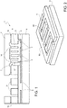
- Figures 1 and 2 show, for example, a generic MEMS sensor 1 obtainable with this process, and comprising forming, on a substrate 2, for example of monocrystalline silicon, a dielectric layer (which partially forms an insulating layer 3); forming, on the dielectric layer, conductive regions 4 (forming electrodes and interconnections); growing, over the dielectric layer and the conductive regions 4, a sacrificial layer (a part whereof is visible in Figure 1 and forms, together with the dielectric layer, the insulating layer 3); etching the sacrificial where it is desired to form anchoring elements to the substrate 2; performing a polycrystalline silicon epitaxial growth, forming anchors 5 and a structural layer 6; performing a dry silicon etch for defining a MEMS structure 7 in the structural layer; and selectively etching the sacrificial layer, for releasing movable elements of the MEMS structure 7.
- Figure 2 shows the structure of first and second fixed electrodes 8A, 8B (generically indicated by 8 in Figure 1 ) and
- the process further comprises final steps including forming metal connection regions 10, and bonding a cap 11 through a bonding layer 12 (for example of glassfrit) .
- a bonding layer 12 for example of glassfrit
- the cap 11 may also be formed of semiconductor material, from a processed silicon wafer, so to have auxiliary structures.
- the cap 11 is recessed at the electrodes 8A, 8B and 9 and has projecting portions 14 directed towards the MEMS structure 7 and forming vertical movement stoppers of the MEMS structure 7 (so-called Z stoppers).
- the cap 11 has a sealing, also hermetic, function and has the aim of protecting the MEMS structure 7 from the external environment (humidity, dust, etc.), as well as from impacts. Its formation from a semiconductor wafer allows to use back-end process technologies such as testing, dicing, packaging and to obtain uniform performance and durability over time of the packaged device.
- inertial devices and, in particular, movement sensors (such as accelerometers, gyroscopes) with high electrical, mechanical and reliability characteristics, at reduced costs, which have determined a significant commercial success thereof, but is liable to improvement.
- movement sensors such as accelerometers, gyroscopes
- the effectiveness and operativeness of the vertical stoppers are linked to the thickness of the bonding layer 12 (typically 5-7 ⁇ m), optimized with respect to its bonding function, and therefore not always with respect to the limitation of the desired vertical movement.
- this solution does not allow two detection structures to be staked in the same packaged device.
- the various devices are arranged adjacent on a support (for example a board) or stacked on each other, resulting in space occupation.
- the possibility of limiting the vertical (out-of-plane) movement of the MEMS structure 7 is limited by the thickness of the bonding layer 12, deriving from implementation considerations not linked to the stop function and thus not always optimized with respect to desired values of the allowed movement.
- Patent application US 2013/0043548 describes a manufacturing process comprising forming, over a first insulating layer extending on substrate, a first polysilicon micromechanical functional layer, which is then patterned to form delimitation trenches having a size that may be subsequently filled with a second insulating layer and form, i.a., pillar structures. Then, part of the first micromechanical functional layer arranged between the pillar structures is selectively removed, to form cavities; a third insulating layer, selectively removed to locally expose the contact regions, is formed over the remaining portions of the first micromechanical functional layer (including contact regions) and of the pillar structures. Then a second micromechanical functional layer is formed and is in direct electrical contact with the contact regions, where the second insulating layer has been removed. Then, the second micromechanical functional layer is defined to form access openings to the lower layers; finally, the third insulating layer, the second insulating layer, the pillar structures and the first insulating layer are selectively removed.
- the process also suffers from limitations, since the height of the first micromechanical functional layer is limited by the ability of the pillar structures to support the second micromechanical functional layer over the cavities and by the criticality of the pillar structures themselves, which have reduced width (due to the width of the trenches manufactured therein).
- the trenches wherein the pillar structures are formed are to be very thin, which may give rise to filling difficulties, with formation of defective pillar structures, which may cause the removal of polycrystalline silicon portions from areas where they should be, during the selective removal process of the first polysilicon and the deposition of polysilicon in the defective trenches in undesired areas.
- the thinness of the pillar structures limits the height thereof.
- US 2011/056295 discloses a micromechanical system formed in different layers, that are deposited, defined and covered by respective insulating layers; the insulating layers fill completely the etching trenches.
- This solution allows forming independent moving elements, but does not allow forming a same sensor structure on different level; in addition, dimensions of the vertical gap and of the trenches and the relative widths of the structural elements on different levels are not freely selectable. In fact, gaps should be thin, trenches should be narrow. In addition, tolerances prevent forming perfectly vertical structures.
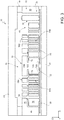
- Figure 3 shows a MEMS device 30 comprising a substrate 31; an insulating layer 32 over the substrate 31; conductive regions 33 over and partially inside the insulating layer 32; a first micromechanical structure 35, here an differential sensor for out-of-plane movement (for example an Z-accelerometer or a gyroscope with pitch and roll movement), having a pair of upper electrodes 36A, 36B and a pair of bottom electrodes 37A, 37B; a Z-stopper structure 38; a second micromechanical structure 40, for example a gyroscope or an accelerometer of reduced thickness, and a cap 44, attached to a fixed portion 45 of the MEMS device 30 through a bonding layer 46.
- a first micromechanical structure 35 here an differential sensor for out-of-plane movement (for example an Z-accelerometer or a gyroscope with pitch and roll movement), having a pair of upper electrodes 36A, 36B and a pair of bottom electrodes 37A, 37B; a Z-stop
- the first and the second micromechanical structures 35, 40, the Z-stopper structure 38 and the fixed portion 45 are formed by two structural layers epitaxially grown on each other (first and second epitaxial layers 41, 42), as described in detail hereinbelow with reference to Figures 4-15 .
- Figure 4 shows a wafer 50 comprising the substrate 31 of semiconductor material, such as monocrystalline silicon; a first dielectric layer 51, for example of silicon oxide, extending over the substrate 31; the conductive regions 33, for example of deposited polycrystalline silicon, extending over the first dielectric layer 51; a first sacrificial layer 53, for example of thermally grown or deposited silicon oxide, which extends over the conductive regions 33 and the first dielectric layer 51; and the first epitaxial layer 41, of silicon, over the first sacrificial layer 53.
- semiconductor material such as monocrystalline silicon
- a first dielectric layer 51 for example of silicon oxide
- the conductive regions 33 for example of deposited polycrystalline silicon
- the first sacrificial layer 53 has first anchoring openings 55 formed through a masking and etching step and accommodating anchoring portions 56 formed by the first epitaxial layer 41.
- the anchoring portions 56 also form electrical contact and biasing structures of the micromechanical structures 35, 40 as well as any other regions and structures of the MEMS device 30.
- the first epitaxial layer 41 has a thickness linked to the desired micro-electro-mechanical structures, which may range, for example, between 2 and 80 ⁇ m. After the epitaxial growth, the first epitaxial layer 41 is planarized and brought to the desired final thickness, for example through CMP (Chemical Mechanical Polishing).
- CMP Chemical Mechanical Polishing
- the first epitaxial layer 41 is etched to define lower portions of the desired structures and other intended regions.
- the wafer 50 is covered by a resist mask (first trench mask), not shown, and subject to a dry etching, thus forming first trenches 58, which extend throughout the first epitaxial layer 41.
- the first trenches 58 are of thin type, with a minimum width (for example of 2 ⁇ m) .
- the etching automatically stops on the first sacrificial layer 53 and leads here to the definition of the bottom electrodes 37A, 37B and of electrodes of the second micromechanical structure 40 as well as of other structures.
- a trench (indicated with 58') is formed for delimiting the first Z-stopper structure 38, as well as any other regions whose definition may not be performed (at least completely) through the second epitaxial layer 42.
- a second sacrificial layer 60 for example of TEOS (Tetraethyl Orthosilicate), is deposited for a thickness comprised, for example, between 1 and 2 ⁇ m.
- the second sacrificial layer 60 partially fills the first trenches 58, for example for a third of their depth (for example for 5-10 ⁇ m), although this filling, as well as the filling extent and depth are not important.
- the second sacrificial layer 60 is planarized.
- the second sacrificial layer 60 is thinned where portions are desired that have the second epitaxial layer 42 projecting downwardly or that are at a reduced distance from the first epitaxial layer 41, as described hereinbelow.
- a masked etching for example time-etching, is performed in a known manner, by using a not-shown masking layer (bump mask), to form grooves 61.
- the grooves 61 extend for example over the bottom electrodes 37A, 37B, where it is desired that the distance between the bottom electrodes 37A, 37B and the upper electrodes 36A, 36B is reduced ( Figure 3 ), to delimit the contact areas that limit the out-of-plane displacements (bump) and to increase the out-of-plane capacitance in the Z-detection areas.
- the grooves 61 may be formed in other zones of the device where desired, as discussed in detail hereinbelow.
- the second sacrificial layer 60 is further etched and selectively removed for its entire thickness, using a masking layer not shown (second anchoring mask), thus forming anchoring openings 62.
- the etching of the second sacrificial layer 60 leads to the formation of hard masking regions 60' and automatically ends on the first epitaxial layer 41.
- the second anchoring openings 62 are formed where connection regions between the first and the second epitaxial layers 41, 42 are desired.
- the second anchoring openings 62 are formed where the second epitaxial layer 42 is anchored to the first epitaxial layer 41, where wide trenches in the first and the second epitaxial layers 41, 42 are desired as well as where alignment structures are desired.
- the hard masking regions 60' have the aim of allowing the definition of structures formed only in the first epitaxial layer 41 and delimited by wide trenches, as discussed hereinbelow.
- the hard masking regions 60' have two different thicknesses: a greater thickness equal to the thickness of the second sacrificial layer 60, and a smaller thickness at the grooves 61.
- the second epitaxial layer 42 is grown, for a thickness here again depending on the desired micro-electro-mechanical structures, and which may be comprised here again between 2 and 80 ⁇ m.
- the second epitaxial layer 42 may be thinner than the first epitaxial layer 41, although the inverse may occur and the invention is not limited to any particular ratio between the thicknesses of the epitaxial layers 41, 42.
- the second epitaxial layer 42 is planarized and brought to the desired final thickness, for example through CMP (Chemical Mechanical Polishing).
- CMP Chemical Mechanical Polishing
- the structural layer formed by the first and the second epitaxial layers 41, 42 also referred to as overall epitaxial layer 64, reaches a final thickness, typically comprised between 20 and 80 ⁇ m.
- electrical connection regions 65 are formed on the upper surface of the overall epitaxial layer 64, by depositing and patterning a metal layer, for example of aluminum or gold, to define the contact pads.
- the wafer 50 is etched.
- the wafer 50 is covered by a resist mask (second trench mask 66) and dry etched.
- the portions of the epitaxial layers 41 and 42 not covered by the second trench mask 66 and not covered by the hard masking regions 60' are removed for the entire thickness of the overall epitaxial layer 64; in these zones, the etching stops on the first sacrificial layer 53.
- the zones not covered by the second trench mask 66 but covered by the hard masking regions 60' are removed for the thickness of the second epitaxial layer 42 only.
- second trenches 67 which extend between and define the upper electrodes 36A, 36B and have depth equal to the thickness of the second epitaxial layer 42; third trenches 68, which extend for the entire thickness of the overall epitaxial layer 64, define and delimit tall structures (here, for example, a carrier pillar region 70 which supports the electrical connection region 65 as well as the fixed portions 45); and cavities 69, which extend through the second epitaxial layer 42 and are delimited on the bottom by the hard masking regions 60', for the formation of structures having height equal to the thickness of the first epitaxial layer 41 (here, for example, at a low region 71 of the second micromechanical structure 40) .
- the second and the third trenches 67, 68 as well as the cavities 69 may be wider than the first trenches 58.
- the second trench mask 66 is removed; then the hard masking regions 60', the portions of the second sacrificial layer 60 inside the first trenches 58, the exposed portions of the first sacrificial layer 53 are removed, releasing the micromechanical structures 35, 40 and the Z-stopper structures 38 and forming first gap zones 77 between the upper electrodes 36A, 36B and the bottom electrodes 37A, 37B and second gap zones 78 below the bottom electrodes 37A, 37B, as well as the other suspended structures (also including electrodes of the second micromechanical structure 40).
- the dielectric layer 51 and the remaining portions of the first sacrificial layer 53 form the insulating layer 32.
- a cap wafer is bonded to the wafer 50 through the bonding layer 46 and the overall wafer is diced to form the MEMS device 30 of Figure 3 .
- the wafer 50 is diced and, on the die thus obtained, the cap 44 is bonded, obtaining the structure of Figure 3 , in a known manner.
- the first micromechanical structure 35 has bottom electrodes 37A, 37B of a first thickness, equal to the thickness of the first epitaxial layer 41; upper electrodes 36A, 36B of a second thickness, here smaller than the first thickness and equal, in first approximation, to the thickness of the second epitaxial layer 42; and a fixed central or anchoring portion 72, of a third thickness, equal, in first approximation, to the sum of the first and the second epitaxial layers 41, 42 (disregarding the thickness of the hard masking regions 60', which is negligible with respect to the thickness of the first and the second epitaxial layers 41, 42, and disregarding the thickness non-uniformity of the second epitaxial layer 42).
- the upper electrodes 36A, 36B have thinner portions 73 (where the hard masking regions 60' had greater thickness, equal to the thickness of the second sacrificial layer 60) and thicker portions 74, where the hard masking regions 60' were thinner.
- the fixed central or anchoring portion 72 forms a supporting structure including a lower supporting portion 72a, an upper supporting portion 72b, an anchoring portion 73c and a neck portion 72d.
- the lower supporting portion is anchored to the substrate 31 by the anchoring portion 73c and the upper supporting portion 72b is coupled to the lower supporting portion 72a by the neck portion 72c.
- the lower supporting portion 72a, the upper supporting portion 72b, the anchoring portion 73c and the neck portion 72d are arranged vertically overlying each other.
- the fixed portion 45 (forming here a perimeter wall surrounding the micromechanical structures 35, 40 and thus hereinafter referred to as wall 45) as well as the carrier pillar region 70 have a thickness equal to the sum of the first and the second epitaxial layers 41, 42.
- the wall 45 also forms a projecting arm 75, extending horizontally inside the MEMS device 30 and overlying, at a distance, an abutment pillar 76, anchored to the substrate 31.
- the projecting arm 75 and the abutment pillar 76 form the first Z-stopper structure 38 and are formed by the second epitaxial layer 42 and the first epitaxial layer 41, respectively, spaced from each other by a space equal to the thickness of the second sacrificial layer 60 ( Figure 7 ) which in this zone had a full thickness, for example 1.6 ⁇ m.
- the distance between the projecting arm 75 and the abutment pillar 76 may be equal to the distance between the upper and bottom electrodes 36, 37 and equal to the thickness of the hard masking regions 60'.
- the abutment pillar 76 is completely surrounded by trenches (part of the first trench 58 and part of the third trench 68), this is not essential, and the abutment pillar 76 may be replaced by a bottom abutment region 76' only partially surrounded, for example, by the first trench 58, as shown in Figure 13A .
- the abutment pillar 76 may be formed by an unanchored portion 76", supported by the first micromechanical structure 35.
- the projecting arm 75 forms an upper abutment region obtainable through a suspended beam but it might be formed by an abutment wall of any shape.
- the Z-movement extent allowed to the micromechanical structures 35, 40 constrained to the substrate 31 may be set to less than 2 ⁇ m and may be controlled precisely through the thickness of the masking regions 60' (with precision of 10%), allowing improved performance in the event of a vertical impact or fall of the MEMS device 30.
- the possibility of forming the electrodes (both upper 36A, 36B and lower 37A, 37B) in two epitaxial layers 41, 42 grown one on top of the other provides improved performance.
- the epitaxial layers 41, 42 are monolithic to each other and have the same mechanical and electrical characteristics. Consequently, they behave in the same manner both towards external stresses (for example in the event that the substrate 31 undergoes a bending), since in this case they would deform in the same manner, and relative to degradation over time.
- the formation of the upper electrodes 36A, 36B and of the bottom electrodes 37A, 37B with central anchoring causes them to be insensitive to stress from the deformation of the substrate and caused by heat treatments or mechanical strains induced on the substrate, for example during soldering in the manufacturing step or during operation.
- FIGS 14-16 show manufacturing steps according to an alternative process.
- Figure 14 shows the wafer 50 after the step of Figure 9 , and thus already comprising the first and the second epitaxial layers 41, 42, embedding the hard masking regions (here referred to as first hard masking regions 60') between each other; the first trenches 58, partially filled with portions of the second sacrificial layer 60, are also present.
- first hard masking regions 60' the hard masking regions
- the electrical connection regions 65 are formed on the second epitaxial layer 42 and the wafer 50 is etched to define the upper electrodes 36A, 36B.
- the wafer 50 is covered by a different second trench mask, indicated herein by 81, and dry etched for removing the exposed portions of the second epitaxial layer 42 only. The etching stops completely here on the first hard masking regions 60' and leads to the formation of the second trenches 67 extending between the upper electrodes 36A, 36B.
- the second trench mask 81 is removed, the electrical connection regions 65 (one in this figure) are formed on the upper surface of the overall epitaxial layer 64 and second hard masking regions 82 are formed on the surface of the wafer 50 to protect the second trenches 67.
- the second hard masking regions 82 are formed by depositing and defining a further sacrificial layer such as TEOS (which may fill here part of the second trenches 67). In this manner, resist, which is more difficult to remove subsequently, is prevented from entering the second trenches 67.
- a third trench mask 85 for example of resist, is formed and covers the surface of the wafer 50, comprising the second hard masking regions 82 and the electrical connection regions 65, and exposes the surface of the overall epitaxial layer 64 where it is desired to form the third trenches 68, extending through the entire overall epitaxial layer 64, or where it is desired to form the cavities 69, extending only through the second epitaxial layer 42, over the lower structures protected by the first hard masking regions 60'.
- the third trench mask 85, the second hard masking regions 82 (comprising the portions inside the second trenches 67), the first hard masking regions 60' (comprising the portions inside the first trenches 58) as well as the exposed portions of the first sacrificial layer 53 are removed, thus releasing the micromechanical structures 35, 40 and forming the first and the second gap zones 77, 78.
- the MEMS device and the manufacturing process described herein have numerous advantages.
- micromechanical structures of a variety of types allow multiple micromechanical structures of a variety of types to be arranged in a single die, allowing the overall size to be reduced, reducing manufacturing costs, improving the integration in portable devices, where the device footprint is important, both in terms of space and costs.
- the size and specifically the thickness of the various regions may be selected very freely, based on the desired structures, and with high dimensional control.
- structures that require high mass such as gyroscopes, in the lower epitaxial layer, and thinner structures, such as accelerometers, in the upper epitaxial layer, may be formed; or the full thickness of the overall epitaxial layer 64 may be used for forming a single structure which requires very high thickness.
- high sensitivity linked to the mass of the sensitive region may be obtained due to the obtainable high thicknesses.
- the process is particularly reliable, since it is based on well-known single process steps and there are no critical intermediate steps or structures.
- the MEMS device has high reliability.
- the process allows to form optimized stop structures that are less sensitive to external influences with respect to the known solutions, such as for example the Z-stopper structure 38 wherein both abutment portions are anchored to the substrate and thus undergo equal stress and deformations, thus making the MEMS device more resistant and reliable.
- a third level may be formed, growing a third epitaxial layer and thus increasing the available height levels and/or the number of integratable structures.
- the process may be used to form drive structures as well, also exploiting different physical principles, for example systems based on electrostatic actuation.
- the Z-stopper structure 38 may be a bottom abutment region 76 in the first epitaxial layer 41 and an upper abutment region 75 in the second epitaxial layer 42 of different shape.
Landscapes
- Engineering & Computer Science (AREA)
- Microelectronics & Electronic Packaging (AREA)
- Manufacturing & Machinery (AREA)
- Computer Hardware Design (AREA)
- Physics & Mathematics (AREA)
- Geometry (AREA)
- Micromachines (AREA)
- Pressure Sensors (AREA)
Abstract
Description
- The present invention relates to a process for manufacturing a micro-electro-mechanical (MEMS) device, in particular a movement sensor with capacitive control/detection and MEMS device thereof.
- Specifically, the considered MEMS device comprises two superimposed structural layers forming at least one structure movable in the plane or out of the plane of one of the structural layers (so called "in-plane" or "out-of-plane" mobile structures); the movable structure may, for example, be a Z-detection sensor and have a first mass or first movable electrodes formed in one of the structural layers, tiltable around a horizontal axis and capacitively coupled to a second mass or to second fixed electrodes formed in the other structural layer.
- In particular, in the following description, reference will be made to a MEMS movement sensor and to the problems for the manufacturing thereof; however the present invention generally applies to other types of MEMS devices.
- For example, the MEMS device may comprise one or more of the following structures, single or coupled to each other (combo): accelerometer, gyroscope, geophone, inclinometer and resonator. Furthermore, the MEMS device may be a MEMS actuator.
- Micromechanical devices of this type are widely used in consumer, automotive and industrial applications.
- As known, during the design of this type of devices, several aspects are to be taken into account, the most relevant whereof are:
- 1) Reduction of device size, in order to reduce manufacturing costs and improve the integration of the device into portable apparata, so that the device has low footprint both in terms of cost and bulk;
- 2) Sensitivity improvement, i.e. high ratio between the variation of the detected signal and the trend of the monitored physical quantity (acceleration/rotation) i.e. between the performed movement and the control signal, in the case of actuators;
- 3) Performance stability in presence of mechanical stress resulting from package, from soldering processes or from temperature;
- 4) Mechanical strength in case of falls and impacts.
- Nowadays, devices of this type are manufactured using different types of technologies. For example, the Applicant has developed a technology comprising the growth of a thick epitaxial layer (which is the structural layer accommodating the detection or actuation structures) over a sacrificial layer that is removed at the end of the manufacturing using hydrofluoric acid vapors.
-
Figures 1 and 2 show, for example, a generic MEMS sensor 1 obtainable with this process, and comprising forming, on asubstrate 2, for example of monocrystalline silicon, a dielectric layer (which partially forms an insulating layer 3); forming, on the dielectric layer, conductive regions 4 (forming electrodes and interconnections); growing, over the dielectric layer and theconductive regions 4, a sacrificial layer (a part whereof is visible inFigure 1 and forms, together with the dielectric layer, the insulating layer 3); etching the sacrificial where it is desired to form anchoring elements to thesubstrate 2; performing a polycrystalline silicon epitaxial growth, forminganchors 5 and astructural layer 6; performing a dry silicon etch for defining aMEMS structure 7 in the structural layer; and selectively etching the sacrificial layer, for releasing movable elements of theMEMS structure 7. For example,Figure 2 shows the structure of first and secondfixed electrodes Figure 1 ) andmovable electrodes 9 of interdigitated type, which form theMEMS structure 7, here a capacitive detection structure. - Typically, the process further comprises final steps including forming
metal connection regions 10, and bonding acap 11 through a bonding layer 12 (for example of glassfrit) . - In particular, the
cap 11 may also be formed of semiconductor material, from a processed silicon wafer, so to have auxiliary structures. For example, inFigure 1 , thecap 11 is recessed at theelectrodes portions 14 directed towards theMEMS structure 7 and forming vertical movement stoppers of the MEMS structure 7 (so-called Z stoppers). - The
cap 11 has a sealing, also hermetic, function and has the aim of protecting theMEMS structure 7 from the external environment (humidity, dust, etc.), as well as from impacts. Its formation from a semiconductor wafer allows to use back-end process technologies such as testing, dicing, packaging and to obtain uniform performance and durability over time of the packaged device. - The process described hereinabove has allowed to manufacture inertial devices and, in particular, movement sensors (such as accelerometers, gyroscopes) with high electrical, mechanical and reliability characteristics, at reduced costs, which have determined a significant commercial success thereof, but is liable to improvement.
- For example, the effectiveness and operativeness of the vertical stoppers (projecting portions 14) are linked to the thickness of the bonding layer 12 (typically 5-7 µm), optimized with respect to its bonding function, and therefore not always with respect to the limitation of the desired vertical movement.
- Furthermore, this solution does not allow two detection structures to be staked in the same packaged device. As a result, when the apparatus using the packaged device uses multiple devices, of different type or intended for the detection on different axes, the various devices are arranged adjacent on a support (for example a board) or stacked on each other, resulting in space occupation.
- Furthermore, the possibility of limiting the vertical (out-of-plane) movement of the
MEMS structure 7 is limited by the thickness of thebonding layer 12, deriving from implementation considerations not linked to the stop function and thus not always optimized with respect to desired values of the allowed movement. - Patent application
US 2013/0043548 describes a manufacturing process comprising forming, over a first insulating layer extending on substrate, a first polysilicon micromechanical functional layer, which is then patterned to form delimitation trenches having a size that may be subsequently filled with a second insulating layer and form, i.a., pillar structures. Then, part of the first micromechanical functional layer arranged between the pillar structures is selectively removed, to form cavities; a third insulating layer, selectively removed to locally expose the contact regions, is formed over the remaining portions of the first micromechanical functional layer (including contact regions) and of the pillar structures. Then a second micromechanical functional layer is formed and is in direct electrical contact with the contact regions, where the second insulating layer has been removed. Then, the second micromechanical functional layer is defined to form access openings to the lower layers; finally, the third insulating layer, the second insulating layer, the pillar structures and the first insulating layer are selectively removed. - However, this process also suffers from limitations, since the height of the first micromechanical functional layer is limited by the ability of the pillar structures to support the second micromechanical functional layer over the cavities and by the criticality of the pillar structures themselves, which have reduced width (due to the width of the trenches manufactured therein). In fact, as emphasized in this document, the trenches wherein the pillar structures are formed are to be very thin, which may give rise to filling difficulties, with formation of defective pillar structures, which may cause the removal of polycrystalline silicon portions from areas where they should be, during the selective removal process of the first polysilicon and the deposition of polysilicon in the defective trenches in undesired areas. Furthermore, the thinness of the pillar structures limits the height thereof.
-
US 2011/056295 discloses a micromechanical system formed in different layers, that are deposited, defined and covered by respective insulating layers; the insulating layers fill completely the etching trenches. This solution allows forming independent moving elements, but does not allow forming a same sensor structure on different level; in addition, dimensions of the vertical gap and of the trenches and the relative widths of the structural elements on different levels are not freely selectable. In fact, gaps should be thin, trenches should be narrow. In addition, tolerances prevent forming perfectly vertical structures. -
DE 10 2013 222 664 A1 teaches a process for manufacturing a MEMS device comprising a complex patterning step to form supporting thin structures that have to completely removed in a final etching, and allows to form a single wide structural portion in the lower structural layer. The process is thus unable to form complex structures with many functional regions extending through both structural layers. Therefore, the aim of the present invention is to provide a solution which overcomes the drawbacks of the prior art. - According to the present invention, a process for manufacturing a MEMS device and a MEMS device are provided, as defined in the attached claims.
- For a better understanding of the present invention, embodiments thereof are now described, purely by way of nonlimiting example, with reference to the attached drawings, wherein:
-
Figure 1 is a cross-section of a known capacitive MEMS sensor; -
Figure 2 is a perspective view, with removed parts, of the sensor ofFigure 1 ; -
Figure 3 is a cross-section of an embodiment of the present MEMS device; -
Figures 4-12 are cross-sectional views of a semiconductor wafer in successive steps for manufacturing the MEMS device ofFigure 3 , according to an embodiment; -
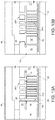
Figures 13A and 13B show different embodiments of a portion of the MEMS device ofFigure 3 ; and -
Figures 14-16 show variations of the steps ofFigures 10-12 , according to a different embodiment of the present process. -
Figure 3 shows aMEMS device 30 comprising asubstrate 31; aninsulating layer 32 over thesubstrate 31;conductive regions 33 over and partially inside theinsulating layer 32; a firstmicromechanical structure 35, here an differential sensor for out-of-plane movement (for example an Z-accelerometer or a gyroscope with pitch and roll movement), having a pair ofupper electrodes bottom electrodes stopper structure 38; a secondmicromechanical structure 40, for example a gyroscope or an accelerometer of reduced thickness, and acap 44, attached to afixed portion 45 of theMEMS device 30 through abonding layer 46. - The first and the second
micromechanical structures stopper structure 38 and thefixed portion 45 are formed by two structural layers epitaxially grown on each other (first and secondepitaxial layers 41, 42), as described in detail hereinbelow with reference toFigures 4-15 . -
Figure 4 shows awafer 50 comprising thesubstrate 31 of semiconductor material, such as monocrystalline silicon; a firstdielectric layer 51, for example of silicon oxide, extending over thesubstrate 31; theconductive regions 33, for example of deposited polycrystalline silicon, extending over the firstdielectric layer 51; a firstsacrificial layer 53, for example of thermally grown or deposited silicon oxide, which extends over theconductive regions 33 and the firstdielectric layer 51; and the firstepitaxial layer 41, of silicon, over the firstsacrificial layer 53. - Over the
conductive regions 33, the firstsacrificial layer 53 hasfirst anchoring openings 55 formed through a masking and etching step and accommodating anchoring portions 56 formed by the firstepitaxial layer 41. The anchoring portions 56 also form electrical contact and biasing structures of themicromechanical structures MEMS device 30. - The first
epitaxial layer 41 has a thickness linked to the desired micro-electro-mechanical structures, which may range, for example, between 2 and 80 µm. After the epitaxial growth, the firstepitaxial layer 41 is planarized and brought to the desired final thickness, for example through CMP (Chemical Mechanical Polishing). - In
Figure 5 , the firstepitaxial layer 41 is etched to define lower portions of the desired structures and other intended regions. To this end, thewafer 50 is covered by a resist mask (first trench mask), not shown, and subject to a dry etching, thus formingfirst trenches 58, which extend throughout the firstepitaxial layer 41. Thefirst trenches 58 are of thin type, with a minimum width (for example of 2 µm) . The etching automatically stops on the firstsacrificial layer 53 and leads here to the definition of thebottom electrodes micromechanical structure 40 as well as of other structures. In particular, in this step, a trench (indicated with 58') is formed for delimiting the first Z-stopper structure 38, as well as any other regions whose definition may not be performed (at least completely) through the secondepitaxial layer 42. - Then,
Figure 6 , a secondsacrificial layer 60, for example of TEOS (Tetraethyl Orthosilicate), is deposited for a thickness comprised, for example, between 1 and 2 µm. The secondsacrificial layer 60 partially fills thefirst trenches 58, for example for a third of their depth (for example for 5-10 µm), although this filling, as well as the filling extent and depth are not important. Then, the secondsacrificial layer 60 is planarized. - In
Figure 7 , the secondsacrificial layer 60 is thinned where portions are desired that have the secondepitaxial layer 42 projecting downwardly or that are at a reduced distance from the firstepitaxial layer 41, as described hereinbelow. To this end, a masked etching, for example time-etching, is performed in a known manner, by using a not-shown masking layer (bump mask), to formgrooves 61. Here, thegrooves 61 extend for example over thebottom electrodes bottom electrodes upper electrodes Figure 3 ), to delimit the contact areas that limit the out-of-plane displacements (bump) and to increase the out-of-plane capacitance in the Z-detection areas. Similarly, and in a not shown manner, thegrooves 61 may be formed in other zones of the device where desired, as discussed in detail hereinbelow. - In
Figure 8 , the secondsacrificial layer 60 is further etched and selectively removed for its entire thickness, using a masking layer not shown (second anchoring mask), thus forminganchoring openings 62. The etching of the secondsacrificial layer 60 leads to the formation of hard maskingregions 60' and automatically ends on thefirst epitaxial layer 41. - In general, the
second anchoring openings 62 are formed where connection regions between the first and the second epitaxial layers 41, 42 are desired. In particular, here, thesecond anchoring openings 62 are formed where thesecond epitaxial layer 42 is anchored to thefirst epitaxial layer 41, where wide trenches in the first and the second epitaxial layers 41, 42 are desired as well as where alignment structures are desired. Furthermore, thehard masking regions 60' have the aim of allowing the definition of structures formed only in thefirst epitaxial layer 41 and delimited by wide trenches, as discussed hereinbelow. - In particular, as a result of the
grooves 61, thehard masking regions 60' have two different thicknesses: a greater thickness equal to the thickness of the secondsacrificial layer 60, and a smaller thickness at thegrooves 61. - Subsequently,
Figure 9 , thesecond epitaxial layer 42 is grown, for a thickness here again depending on the desired micro-electro-mechanical structures, and which may be comprised here again between 2 and 80 µm. In general, thesecond epitaxial layer 42 may be thinner than thefirst epitaxial layer 41, although the inverse may occur and the invention is not limited to any particular ratio between the thicknesses of theepitaxial layers - After the epitaxial growth, the
second epitaxial layer 42 is planarized and brought to the desired final thickness, for example through CMP (Chemical Mechanical Polishing). In this manner, the structural layer formed by the first and the second epitaxial layers 41, 42, also referred to asoverall epitaxial layer 64, reaches a final thickness, typically comprised between 20 and 80 µm. - In
Figure 10 , electrical connection regions 65 (one in figure) are formed on the upper surface of theoverall epitaxial layer 64, by depositing and patterning a metal layer, for example of aluminum or gold, to define the contact pads. - In
Figure 11 , thewafer 50 is etched. To this end, thewafer 50 is covered by a resist mask (second trench mask 66) and dry etched. In this step, the portions of theepitaxial layers second trench mask 66 and not covered by thehard masking regions 60' are removed for the entire thickness of theoverall epitaxial layer 64; in these zones, the etching stops on the firstsacrificial layer 53. Conversely, the zones not covered by thesecond trench mask 66 but covered by thehard masking regions 60' are removed for the thickness of thesecond epitaxial layer 42 only. - In particular, in this step,
second trenches 67, which extend between and define theupper electrodes second epitaxial layer 42;third trenches 68, which extend for the entire thickness of theoverall epitaxial layer 64, define and delimit tall structures (here, for example, acarrier pillar region 70 which supports theelectrical connection region 65 as well as the fixed portions 45); andcavities 69, which extend through thesecond epitaxial layer 42 and are delimited on the bottom by thehard masking regions 60', for the formation of structures having height equal to the thickness of the first epitaxial layer 41 (here, for example, at alow region 71 of the second micromechanical structure 40) . - In some areas, the second and the
third trenches cavities 69 may be wider than thefirst trenches 58. - Subsequently,
Figure 12 , thesecond trench mask 66 is removed; then thehard masking regions 60', the portions of the secondsacrificial layer 60 inside thefirst trenches 58, the exposed portions of the firstsacrificial layer 53 are removed, releasing themicromechanical structures stopper structures 38 and formingfirst gap zones 77 between theupper electrodes bottom electrodes second gap zones 78 below thebottom electrodes - Thus, the
dielectric layer 51 and the remaining portions of the firstsacrificial layer 53 form the insulatinglayer 32. - Finally, a cap wafer is bonded to the
wafer 50 through thebonding layer 46 and the overall wafer is diced to form theMEMS device 30 ofFigure 3 . Alternatively, thewafer 50 is diced and, on the die thus obtained, thecap 44 is bonded, obtaining the structure ofFigure 3 , in a known manner. - In this manner, and referring again to
Figure 3 , the firstmicromechanical structure 35 hasbottom electrodes first epitaxial layer 41;upper electrodes second epitaxial layer 42; and a fixed central or anchoringportion 72, of a third thickness, equal, in first approximation, to the sum of the first and the second epitaxial layers 41, 42 (disregarding the thickness of thehard masking regions 60', which is negligible with respect to the thickness of the first and the second epitaxial layers 41, 42, and disregarding the thickness non-uniformity of the second epitaxial layer 42). Furthermore, theupper electrodes hard masking regions 60' had greater thickness, equal to the thickness of the second sacrificial layer 60) andthicker portions 74, where thehard masking regions 60' were thinner. - In particular, the fixed central or anchoring
portion 72 forms a supporting structure including a lower supporting portion 72a, an upper supporting portion 72b, an anchoring portion 73c and a neck portion 72d. The lower supporting portion is anchored to thesubstrate 31 by the anchoring portion 73c and the upper supporting portion 72b is coupled to the lower supporting portion 72a by the neck portion 72c. In addition, the lower supporting portion 72a, the upper supporting portion 72b, the anchoring portion 73c and the neck portion 72d are arranged vertically overlying each other. - Furthermore, the fixed portion 45 (forming here a perimeter wall surrounding the
micromechanical structures carrier pillar region 70 have a thickness equal to the sum of the first and the second epitaxial layers 41, 42. - In the
MEMS device 30 ofFigure 3 , thewall 45 also forms a projectingarm 75, extending horizontally inside theMEMS device 30 and overlying, at a distance, anabutment pillar 76, anchored to thesubstrate 31. - The projecting
arm 75 and theabutment pillar 76 form the first Z-stopper structure 38 and are formed by thesecond epitaxial layer 42 and thefirst epitaxial layer 41, respectively, spaced from each other by a space equal to the thickness of the second sacrificial layer 60 (Figure 7 ) which in this zone had a full thickness, for example 1.6 µm. Alternatively, if acavity 61 is formed also in this area, the distance between the projectingarm 75 and theabutment pillar 76 may be equal to the distance between the upper and bottom electrodes 36, 37 and equal to the thickness of thehard masking regions 60'. - Furthermore, although in
Figures 3-12 theabutment pillar 76 is completely surrounded by trenches (part of thefirst trench 58 and part of the third trench 68), this is not essential, and theabutment pillar 76 may be replaced by a bottom abutment region 76' only partially surrounded, for example, by thefirst trench 58, as shown inFigure 13A . - According to another alternative, shown in
Figure 13B , theabutment pillar 76 may be formed by anunanchored portion 76", supported by the firstmicromechanical structure 35. - The projecting
arm 75 forms an upper abutment region obtainable through a suspended beam but it might be formed by an abutment wall of any shape. - In this manner, the Z-movement extent allowed to the
micromechanical structures substrate 31 may be set to less than 2 µm and may be controlled precisely through the thickness of the maskingregions 60' (with precision of 10%), allowing improved performance in the event of a vertical impact or fall of theMEMS device 30. - Furthermore, the possibility of forming the electrodes (both upper 36A, 36B and lower 37A, 37B) in two
epitaxial layers MEMS device 30 is finished, theepitaxial layers substrate 31 undergoes a bending), since in this case they would deform in the same manner, and relative to degradation over time. The formation of theupper electrodes bottom electrodes -
Figures 14-16 show manufacturing steps according to an alternative process. - In detail,
Figure 14 shows thewafer 50 after the step ofFigure 9 , and thus already comprising the first and the second epitaxial layers 41, 42, embedding the hard masking regions (here referred to as firsthard masking regions 60') between each other; thefirst trenches 58, partially filled with portions of the secondsacrificial layer 60, are also present. - In
Figure 14 , the electrical connection regions 65 (one in this figure) are formed on thesecond epitaxial layer 42 and thewafer 50 is etched to define theupper electrodes wafer 50 is covered by a different second trench mask, indicated herein by 81, and dry etched for removing the exposed portions of thesecond epitaxial layer 42 only. The etching stops completely here on the firsthard masking regions 60' and leads to the formation of thesecond trenches 67 extending between theupper electrodes - Then,
Figure 15 , thesecond trench mask 81 is removed, the electrical connection regions 65 (one in this figure) are formed on the upper surface of theoverall epitaxial layer 64 and secondhard masking regions 82 are formed on the surface of thewafer 50 to protect thesecond trenches 67. For example, the secondhard masking regions 82 are formed by depositing and defining a further sacrificial layer such as TEOS (which may fill here part of the second trenches 67). In this manner, resist, which is more difficult to remove subsequently, is prevented from entering thesecond trenches 67. - Subsequently, a
third trench mask 85, for example of resist, is formed and covers the surface of thewafer 50, comprising the secondhard masking regions 82 and theelectrical connection regions 65, and exposes the surface of theoverall epitaxial layer 64 where it is desired to form thethird trenches 68, extending through the entireoverall epitaxial layer 64, or where it is desired to form thecavities 69, extending only through thesecond epitaxial layer 42, over the lower structures protected by the firsthard masking regions 60'. - Then,
Figure 16 , the second and the first epitaxial layers 42, 41 are selectively removed, forming thethird trenches 68 and thecavities 69. - Then, the
third trench mask 85, the second hard masking regions 82 (comprising the portions inside the second trenches 67), the firsthard masking regions 60' (comprising the portions inside the first trenches 58) as well as the exposed portions of the firstsacrificial layer 53 are removed, thus releasing themicromechanical structures second gap zones - Then, the final steps already described with reference to
Figure 12 and leading to theMEMS device 30 ofFigure 3 follow. - With the solution of
Figures 14-16 , a high dimensional precision may be obtained, since the size of the openings in the second trench mask 81 (intended for the definition of the second, narrower, trenches 67) and in the third trench mask 85 (intended for the definition of the third, wider,trenches 68 and of the cavities 69) may be better controlled with reference to the specific widths of the trenches and of the zones to be removed. - The MEMS device and the manufacturing process described herein have numerous advantages.
- In particular, they allow multiple micromechanical structures of a variety of types to be arranged in a single die, allowing the overall size to be reduced, reducing manufacturing costs, improving the integration in portable devices, where the device footprint is important, both in terms of space and costs.
- The size and specifically the thickness of the various regions may be selected very freely, based on the desired structures, and with high dimensional control. For example, structures that require high mass, such as gyroscopes, in the lower epitaxial layer, and thinner structures, such as accelerometers, in the upper epitaxial layer, may be formed; or the full thickness of the
overall epitaxial layer 64 may be used for forming a single structure which requires very high thickness. In general, high sensitivity, linked to the mass of the sensitive region may be obtained due to the obtainable high thicknesses. - Furthermore, as explained, it is possible to form structures with at least three different base heights, which may be modulated as explained hereinabove for the
upper electrodes - The process is particularly reliable, since it is based on well-known single process steps and there are no critical intermediate steps or structures. Thus, the MEMS device has high reliability.
- It is possible to stack two or more different structures, which are monolithic to each other and thus have high behavioral uniformity and stability with regard to manufacturing imperfections and spreads, disturbances and external actions, stress and variations over time.
- The process allows to form optimized stop structures that are less sensitive to external influences with respect to the known solutions, such as for example the Z-
stopper structure 38 wherein both abutment portions are anchored to the substrate and thus undergo equal stress and deformations, thus making the MEMS device more resistant and reliable. - Finally, it is clear that modifications and variations may be made to the manufacturing process and to the MEMS device described and illustrated herein without thereby departing from the protective scope of the present invention, as defined in the attached claims.
- For example, if desired, a third level may be formed, growing a third epitaxial layer and thus increasing the available height levels and/or the number of integratable structures.
- Furthermore, although the structures shown are capacitive sensors, the process may be used to form drive structures as well, also exploiting different physical principles, for example systems based on electrostatic actuation.
- As discussed hereinabove, the Z-
stopper structure 38 may be abottom abutment region 76 in thefirst epitaxial layer 41 and anupper abutment region 75 in thesecond epitaxial layer 42 of different shape.
Claims (16)
- A process for manufacturing a MEMS device (30) comprising:forming a first structural layer (41) of semiconductor material on a substrate (31), the first structural layer having a first thickness;forming a plurality of first trenches (58) extending through the first structural layer (41) and defining first functional elements (37A, 37B);forming masking regions (60') on the first structural layer, the masking regions being separated from each other by first openings (62);forming a second structural layer (42) of semiconductor material on the first structural layer (41) and on the masking regions (60'), the second structural layer having a second thickness, being in direct contact with the first structural layer (41) at the first openings (62) and forming here, together with the first structural layer, thick structural regions (64) of the semiconductor material having a third thickness equal to the sum of the first and the second thicknesses;forming a plurality of second trenches (67) extending through the second structural layer (42), over the masking regions (60'), and delimiting second functional elements (36A, 36B) having the second thickness; andforming a plurality of third trenches (68) extending through the first and the second structural layers (41, 42) by removing selective portions of the thick structural regions (64), the third trenches (68) delimiting third functional elements (45, 70) having the third thickness.
- The process according to the preceding claim, further comprising, while forming the third trenches (68), removing selective portions of the second structural layer (42) to form cavities (69) over the masking regions (60'), thereby forming fourth functional regions (71) having the first thickness.
- The process according to claim 1 or 2, wherein forming second trenches (67) and forming third trenches (68) comprise using a single etching mask (66).
- The process according to claim 1 or 2, wherein forming second trenches (67) and forming third trenches (68) comprise using two distinct etching masks (81, 85).
- The process according to any of the preceding claims, wherein the third trenches (68) have greater width than the second trenches (67).
- The process according to any of the preceding claims, wherein forming masking regions (60') comprises forming a masking sacrificial layer (60) extending on the first structural layer and only partially in the first trenches (58) and patterning the masking sacrificial layer.
- The process according to any of the preceding claims, further comprising removing the masking regions (60') and forming first gap zones (77) between the first and the second structural layers (41, 42).
- The process according to the preceding claim, comprising, before forming a first structural layer (41), forming a sacrificial anchoring layer (53) over the substrate (31), the sacrificial anchoring layer having anchoring openings (55), and removing the masking regions (60') comprises removing the sacrificial anchoring layer (53) and forming second gap zones (78) between the first structural layer (41) and the substrate (31).
- The process according to any of the preceding claims, comprising forming a vertical stop structure (38) including forming a bottom abutment region (76) in the first structural layer (41) and forming an upper abutment region (75) in the second structural layer (42), the bottom abutment region (76) having the first thickness and being delimited, at least partially, by a first trench (58) belonging to the plurality of first trenches and/or by a lower portion of an abutment trench (68) belonging to the plurality of third trenches (68) and the upper abutment region (75) overlying the bottom abutment region (76), being separated from the bottom abutment region by a first gap zone (77) of the plurality of first gap zones.
- The process according to the preceding claim, wherein the upper abutment region (75) is delimited by a second trench (68) belonging to the plurality of second trenches and/or by an upper part of the abutment trench (68) .
- A MEMS device (30) comprising:a substrate (31);a first structural layer (41) having a first thickness and extending on the substrate;a second structural layer (42) having a second thickness and extending on the first structural layer;a plurality of first trenches (58) extending through the first structural layer (41) and delimiting first functional elements (37A, 37B) having the first thickness;a plurality of second trenches (67) extending through the second structural layer (42) and delimiting second functional elements (36A, 36B) having the second thickness and superimposed to the first functional elements; anda plurality of third trenches (68) extending through the first and the second structural layers (41, 42) and delimiting third functional elements (45, 70) having a third thickness equal to the sum of the first and the second thicknesses,wherein the first and the second structural layers form a supporting structure (72), having the third thickness, anchored to the substrate (31) and supporting the first and/or the second functional elements (37A, 37B, 36A, 36B), andwherein a first gap zone (77) extends between the first and the second functional elements and surrounds the supporting structure (72).
- The MEMS device according to the preceding claim, further comprising:a vertical stop structure (38) including a bottom abutment region (76) and an upper abutment region (75), the upper abutment region overlying the bottom abutment region,the bottom abutment region (76) extending in the first structural layer (41), having the first thickness and being delimited, at least partially, by a first trench (58) belonging to the plurality of first trenches and/or by a lower portion of an abutment trench (68) belonging to the plurality of third trenches, andthe upper abutment region (75) extending in the second structural layer (42), having the second thickness, and separated from the bottom abutment region (75) by an abutment gap area (77).
- The MEMS device according to the preceding claim, wherein the upper abutment region (75) is delimited by a second trench (68) belonging to the plurality of second trenches and/or by an upper part of the abutment trench (68) .
- The MEMS device according to any of claims 11-13, further comprising:first functional regions (75) having the second thickness and delimited by the second or the third trenches (67, 68);second functional regions (70) having the third thickness and delimited by the third trenches (68); andthird functional regions (71) having the first thickness and delimited by the first trenches (58) and/or by lower portions of the third trenches (68).
- The MEMS device according to the preceding claim, comprising a dielectric layer (51) extending on the substrate (31) and conductive regions (33), extending on the dielectric layer (51) and selectively coupled to the supporting structure (72) and to the first, second and/or third functional regions (75, 70, 71).
- The MEMS device according to any of claims 11-15, wherein the second functional elements (36A, 36B) have a width which is greater than the width of the first functional elements (37A, 37B) .
Applications Claiming Priority (1)
| Application Number | Priority Date | Filing Date | Title |
|---|---|---|---|
| IT102020000011755A IT202000011755A1 (en) | 2020-05-20 | 2020-05-20 | MANUFACTURING PROCESS OF A MICRO-ELECTRO-MECHANICAL DEVICE, IN PARTICULAR MOVEMENT SENSOR WITH CAPACITIVE COMMAND/DETECTION, AND RELATED MEMS DEVICE |
Publications (2)
| Publication Number | Publication Date |
|---|---|
| EP3912953A1 true EP3912953A1 (en) | 2021-11-24 |
| EP3912953B1 EP3912953B1 (en) | 2024-06-26 |
Family
ID=71784582
Family Applications (1)
| Application Number | Title | Priority Date | Filing Date |
|---|---|---|---|
| EP21174844.7A Active EP3912953B1 (en) | 2020-05-20 | 2021-05-19 | Process for manufacturing a micro-electro-mechanical device, in particular a movement sensor with capacitive control/detection, and mems device |
Country Status (4)
| Country | Link |
|---|---|
| US (2) | US11945712B2 (en) |
| EP (1) | EP3912953B1 (en) |
| CN (2) | CN113697766B (en) |
| IT (1) | IT202000011755A1 (en) |
Cited By (6)
| Publication number | Priority date | Publication date | Assignee | Title |
|---|---|---|---|---|
| IT202200000524A1 (en) | 2022-01-14 | 2023-07-14 | St Microelectronics Srl | MICROELECTROMECHANICAL GYROSCOPE WITH OUT-OF-PLANE SENSING MOVEMENT HAVING IMPROVED ELECTRICAL CHARACTERISTICS |
| IT202200002150A1 (en) | 2022-02-07 | 2023-08-07 | Milano Politecnico | PULL-IN RESILIENT LONG STROKE MEMS ACTUATOR AND ELECTRONIC SYSTEM INCLUDING THE SAME |
| IT202200022377A1 (en) | 2022-10-31 | 2024-05-01 | St Microelectronics Srl | MICROELECTROMECHANICAL GYROSCOPE WITH ANGULAR VELOCITY DETECTION ALONG A VERTICAL AXIS |
| IT202200024732A1 (en) | 2022-11-30 | 2024-05-30 | St Microelectronics Srl | MICROELECTROMECHANICAL DEVICE WITH TEST STRUCTURE, TEST EQUIPMENT FOR TESTING MICROELECTROMECHANICAL DEVICES AND METHOD FOR MANUFACTURING A MICROELECTROMECHANICAL DEVICE |
| DE102023209211A1 (en) | 2023-09-21 | 2025-03-27 | Robert Bosch Gesellschaft mit beschränkter Haftung | Method for producing a microelectromechanical component structure, microelectromechanical component structure, microelectromechanical device and microelectromechanical loudspeaker |
| IT202300023175A1 (en) | 2023-11-03 | 2025-05-03 | St Microelectronics Int Nv | MICRO-ELECTRO-MECHANICAL DEVICE HAVING MOISTURE-PROOF CONTACT PADS AND RELATED MANUFACTURING PROCESS |
Families Citing this family (8)
| Publication number | Priority date | Publication date | Assignee | Title |
|---|---|---|---|---|
| IT202000011755A1 (en) * | 2020-05-20 | 2021-11-20 | St Microelectronics Srl | MANUFACTURING PROCESS OF A MICRO-ELECTRO-MECHANICAL DEVICE, IN PARTICULAR MOVEMENT SENSOR WITH CAPACITIVE COMMAND/DETECTION, AND RELATED MEMS DEVICE |
| US12325628B2 (en) | 2021-05-25 | 2025-06-10 | Stmicroelectronics S.R.L. | Microelectromechanical device with out-of-plane stopper structure |
| EP4123313B1 (en) | 2021-07-23 | 2024-11-13 | STMicroelectronics S.r.l. | Closed-loop microelectromechanical accelerometer with compensation of spurious vibration modes and process for manufacturing a microelectromechanical accelerometer |
| EP4187258A1 (en) * | 2021-11-25 | 2023-05-31 | STMicroelectronics S.r.l. | Z-axis microelectromechanical sensor device with improved stress insensitivity |
| CN114715833B (en) * | 2022-04-11 | 2024-08-13 | 中国兵器工业集团第二一四研究所苏州研发中心 | MEMS device for preventing vertical gap adhesion and manufacturing method thereof |
| IT202300001191A1 (en) | 2023-01-26 | 2024-07-26 | St Microelectronics Srl | CAPACITIVE MEMS ACOUSTIC TRANSDUCER, HAVING SEPARATE SENSING AREA AND TRANSDUCTION AREA, AND RELATED MANUFACTURING PROCESS |
| EP4421022A1 (en) | 2023-02-27 | 2024-08-28 | Murata Manufacturing Co., Ltd. | Double layer mems devices |
| US12565417B2 (en) * | 2023-04-10 | 2026-03-03 | AAC Technologies Pte. Ltd. | MEMS device and manufacturing method thereof |
Citations (4)
| Publication number | Priority date | Publication date | Assignee | Title |
|---|---|---|---|---|
| US20100297781A1 (en) * | 2006-07-12 | 2010-11-25 | Robert Bosch Gmbh | Method for manufacturing mems structures |
| US20110056295A1 (en) | 2009-09-04 | 2011-03-10 | Johannes Classen | Micromechanical system |
| US20130043548A1 (en) | 2011-08-16 | 2013-02-21 | Jochen Reinmuth | Method for manufacturing a micromechanical structure, and micromechanical structure |
| DE102013222664A1 (en) | 2013-11-07 | 2015-05-07 | Robert Bosch Gmbh | Micromechanical structure and method for producing a micromechanical structure |
Family Cites Families (16)
| Publication number | Priority date | Publication date | Assignee | Title |
|---|---|---|---|---|
| DE19847455A1 (en) * | 1998-10-15 | 2000-04-27 | Bosch Gmbh Robert | Silicon multi-layer etching, especially for micromechanical sensor production, comprises etching trenches down to buried separation layer, etching exposed separation layer and etching underlying silicon layer |
| DE60032772T2 (en) * | 2000-09-27 | 2007-11-08 | Stmicroelectronics S.R.L., Agrate Brianza | Integrated chemical microreactor with thermally insulated measuring electrodes and method for its production |
| EP1624284B1 (en) | 2004-07-29 | 2017-07-19 | STMicroelectronics Srl | Mems-type high-sensitivity inertial sensor and manufacturing process thereof |
| DE102006051597A1 (en) * | 2006-11-02 | 2008-05-08 | Atmel Germany Gmbh | Semiconductor arrangement and method for producing a semiconductor device |
| US7943525B2 (en) * | 2008-12-19 | 2011-05-17 | Freescale Semiconductor, Inc. | Method of producing microelectromechanical device with isolated microstructures |
| ITTO20090616A1 (en) * | 2009-08-05 | 2011-02-06 | St Microelectronics Srl | PROCESS OF MANUFACTURING OF MEMS DEVICES EQUIPPED WITH CUTTED CAVITIES AND MEMS DEVICE SO OBTAINED |
| US10160632B2 (en) * | 2012-08-21 | 2018-12-25 | Robert Bosch Gmbh | System and method for forming a buried lower electrode in conjunction with an encapsulated MEMS device |
| US9073749B2 (en) * | 2012-12-05 | 2015-07-07 | Robert Bosch Gmbh | Structured gap for a MEMS pressure sensor |
| US9006015B2 (en) * | 2013-01-24 | 2015-04-14 | Taiwan Semiconductor Manfacturing Company, Ltd. | Dual layer microelectromechanical systems device and method of manufacturing same |
| US9434602B2 (en) * | 2014-07-30 | 2016-09-06 | Freescale Semiconductor, Inc. | Reducing MEMS stiction by deposition of nanoclusters |
| ITUB20155716A1 (en) * | 2015-11-19 | 2017-05-19 | St Microelectronics Srl | MICRO-ELECTRO-MECHANICAL DEVICE EQUIPPED WITH TWO CAVITIES AND RELATIVE PROCESS OF MANUFACTURE |
| EP3397585B1 (en) * | 2015-12-30 | 2019-11-06 | Robert Bosch GmbH | System and method for maintaining a smoothed and anti-stiction surface on a mems device |
| ITUA20162174A1 (en) * | 2016-03-31 | 2017-10-01 | St Microelectronics Srl | PROCESS OF MANUFACTURE OF A MEMS PRESSURE SENSOR AND RELATIVE MEMS PRESSURE SENSOR |
| DE102020205170A1 (en) * | 2020-04-23 | 2021-10-28 | Robert Bosch Gesellschaft mit beschränkter Haftung | Method for producing a micromechanical structure and micromechanical structure |
| IT202000011755A1 (en) * | 2020-05-20 | 2021-11-20 | St Microelectronics Srl | MANUFACTURING PROCESS OF A MICRO-ELECTRO-MECHANICAL DEVICE, IN PARTICULAR MOVEMENT SENSOR WITH CAPACITIVE COMMAND/DETECTION, AND RELATED MEMS DEVICE |
| US12139396B2 (en) | 2020-08-07 | 2024-11-12 | Stmicroelectronics S.R.L. | Microelectromechanical sensor device with improved stability to stress |
-
2020
- 2020-05-20 IT IT102020000011755A patent/IT202000011755A1/en unknown
-
2021
- 2021-05-14 US US17/320,993 patent/US11945712B2/en active Active
- 2021-05-19 CN CN202110545660.8A patent/CN113697766B/en active Active
- 2021-05-19 EP EP21174844.7A patent/EP3912953B1/en active Active
- 2021-05-19 CN CN202121072705.6U patent/CN215756431U/en not_active Withdrawn - After Issue
-
2024
- 2024-02-28 US US18/590,533 patent/US20240199408A1/en not_active Abandoned
Patent Citations (4)
| Publication number | Priority date | Publication date | Assignee | Title |
|---|---|---|---|---|
| US20100297781A1 (en) * | 2006-07-12 | 2010-11-25 | Robert Bosch Gmbh | Method for manufacturing mems structures |
| US20110056295A1 (en) | 2009-09-04 | 2011-03-10 | Johannes Classen | Micromechanical system |
| US20130043548A1 (en) | 2011-08-16 | 2013-02-21 | Jochen Reinmuth | Method for manufacturing a micromechanical structure, and micromechanical structure |
| DE102013222664A1 (en) | 2013-11-07 | 2015-05-07 | Robert Bosch Gmbh | Micromechanical structure and method for producing a micromechanical structure |
Non-Patent Citations (1)
| Title |
|---|
| CLASSEN JOHANNES ET AL: "Advanced surface micromachining process - A first step towards 3D MEMS", 2017 IEEE 30TH INTERNATIONAL CONFERENCE ON MICRO ELECTRO MECHANICAL SYSTEMS (MEMS), IEEE, 22 January 2017 (2017-01-22), pages 314 - 318, XP033069521, DOI: 10.1109/MEMSYS.2017.7863404 * |
Cited By (12)
| Publication number | Priority date | Publication date | Assignee | Title |
|---|---|---|---|---|
| IT202200000524A1 (en) | 2022-01-14 | 2023-07-14 | St Microelectronics Srl | MICROELECTROMECHANICAL GYROSCOPE WITH OUT-OF-PLANE SENSING MOVEMENT HAVING IMPROVED ELECTRICAL CHARACTERISTICS |
| EP4212824A1 (en) | 2022-01-14 | 2023-07-19 | STMicroelectronics S.r.l. | Microelectromechanical gyroscope with out-of-plane detection movement having improved electrical characteristics |
| IT202200002150A1 (en) | 2022-02-07 | 2023-08-07 | Milano Politecnico | PULL-IN RESILIENT LONG STROKE MEMS ACTUATOR AND ELECTRONIC SYSTEM INCLUDING THE SAME |
| EP4223691A1 (en) | 2022-02-07 | 2023-08-09 | STMicroelectronics S.r.l. | Long stroke mems actuator resilient to the pull-in and electronic system including the same |
| IT202200022377A1 (en) | 2022-10-31 | 2024-05-01 | St Microelectronics Srl | MICROELECTROMECHANICAL GYROSCOPE WITH ANGULAR VELOCITY DETECTION ALONG A VERTICAL AXIS |
| EP4361560A1 (en) | 2022-10-31 | 2024-05-01 | STMicroelectronics S.r.l. | Microelectromechanical gyroscope with detection of angular velocity along a vertical axis |
| IT202200024732A1 (en) | 2022-11-30 | 2024-05-30 | St Microelectronics Srl | MICROELECTROMECHANICAL DEVICE WITH TEST STRUCTURE, TEST EQUIPMENT FOR TESTING MICROELECTROMECHANICAL DEVICES AND METHOD FOR MANUFACTURING A MICROELECTROMECHANICAL DEVICE |
| EP4379320A1 (en) | 2022-11-30 | 2024-06-05 | STMicroelectronics S.r.l. | Microelectromechanical device with test structure, test equipment for testing microelectromechanical devices and method for manufacturing a microelectromechanical device |
| DE102023209211A1 (en) | 2023-09-21 | 2025-03-27 | Robert Bosch Gesellschaft mit beschränkter Haftung | Method for producing a microelectromechanical component structure, microelectromechanical component structure, microelectromechanical device and microelectromechanical loudspeaker |
| WO2025061619A1 (en) | 2023-09-21 | 2025-03-27 | Robert Bosch Gmbh | Method for producing a microelectromechanical component structure, microelectromechanical component structure, microelectromechanical device and microelectromechanical loudspeaker |
| IT202300023175A1 (en) | 2023-11-03 | 2025-05-03 | St Microelectronics Int Nv | MICRO-ELECTRO-MECHANICAL DEVICE HAVING MOISTURE-PROOF CONTACT PADS AND RELATED MANUFACTURING PROCESS |
| EP4549372A1 (en) | 2023-11-03 | 2025-05-07 | STMicroelectronics International N.V. | Micro-electro-mechanical device having contact pads that are protected against humidity and manufacturing process thereof |
Also Published As
| Publication number | Publication date |
|---|---|
| CN215756431U (en) | 2022-02-08 |
| IT202000011755A1 (en) | 2021-11-20 |
| US20210363000A1 (en) | 2021-11-25 |
| EP3912953B1 (en) | 2024-06-26 |
| US11945712B2 (en) | 2024-04-02 |
| US20240199408A1 (en) | 2024-06-20 |
| CN113697766A (en) | 2021-11-26 |
| CN113697766B (en) | 2025-07-11 |
Similar Documents
| Publication | Publication Date | Title |
|---|---|---|
| EP3912953B1 (en) | Process for manufacturing a micro-electro-mechanical device, in particular a movement sensor with capacitive control/detection, and mems device | |
| US6951824B2 (en) | Method for manufacturing a micromechanical component and a component that is manufactured in accordance with the method | |
| EP2023151B1 (en) | Sensor with position-indepedent drive electrodes in multi-layer silicon on insulator substrate | |
| EP1617227A2 (en) | Inertial sensor | |
| US7943525B2 (en) | Method of producing microelectromechanical device with isolated microstructures | |
| US7437933B2 (en) | Micro-electro-mechanical structure having electrically insulated regions and manufacturing process thereof | |
| EP1423714B1 (en) | Microstructure with movable mass | |
| US20100024549A1 (en) | In-Plane Sensor, Out-of-Plane Sensor, and Method for Making Same | |
| JP7764909B2 (en) | MEMS device and manufacturing method thereof | |
| US6694504B2 (en) | Method of fabricating an electrostatic vertical and torsional actuator using one single-crystalline silicon wafer | |
| US11267697B2 (en) | Use of an uncoupling structure for assembling a component having a casing | |
| US7063796B2 (en) | Micromechanical component and method for producing the same | |
| US7243546B2 (en) | Acceleration sensor chip | |
| WO2003065052A2 (en) | Method of manufacturing an accelerometer | |
| US7326586B2 (en) | Method for manufacturing semiconductor physical quantity sensor | |
| US20020104379A1 (en) | Accelerometer with re-entrant grooves | |
| US8430255B2 (en) | Method of accurately spacing Z-axis electrode | |
| CN117342516A (en) | Manufacturing method of MEMS vertical electrode structure | |
| EP4079679B1 (en) | Method for etching gaps of unequal width | |
| US20250145453A1 (en) | Micro-electro-mechanical device having contact pads that are protected against humidity and manufacturing process thereof | |
| US20240300808A1 (en) | Mems stress isolation technology with backside etched isolation trenches | |
| EP4474341A1 (en) | Mems device with a cap layer having gaps and method of manufacturing a mems device | |
| JP2004317478A (en) | Semiconductor acceleration sensor and its manufacturing method | |
| KR100620288B1 (en) | Vacuum Floating Structure Using Gap Filler and Formation Method Thereof | |
| CN121195172A (en) | Electrostatic capacitive sensor and its manufacturing method |
Legal Events
| Date | Code | Title | Description |
|---|---|---|---|
| PUAI | Public reference made under article 153(3) epc to a published international application that has entered the european phase |
Free format text: ORIGINAL CODE: 0009012 |
|
| STAA | Information on the status of an ep patent application or granted ep patent |
Free format text: STATUS: THE APPLICATION HAS BEEN PUBLISHED |
|
| AK | Designated contracting states |
Kind code of ref document: A1 Designated state(s): AL AT BE BG CH CY CZ DE DK EE ES FI FR GB GR HR HU IE IS IT LI LT LU LV MC MK MT NL NO PL PT RO RS SE SI SK SM TR |
|
| B565 | Issuance of search results under rule 164(2) epc |
Effective date: 20211011 |
|
| STAA | Information on the status of an ep patent application or granted ep patent |
Free format text: STATUS: REQUEST FOR EXAMINATION WAS MADE |
|
| 17P | Request for examination filed |
Effective date: 20220523 |
|
| RBV | Designated contracting states (corrected) |
Designated state(s): AL AT BE BG CH CY CZ DE DK EE ES FI FR GB GR HR HU IE IS IT LI LT LU LV MC MK MT NL NO PL PT RO RS SE SI SK SM TR |
|
| GRAP | Despatch of communication of intention to grant a patent |
Free format text: ORIGINAL CODE: EPIDOSNIGR1 |
|
| STAA | Information on the status of an ep patent application or granted ep patent |
Free format text: STATUS: GRANT OF PATENT IS INTENDED |
|
| INTG | Intention to grant announced |
Effective date: 20231219 |
|
| GRAS | Grant fee paid |
Free format text: ORIGINAL CODE: EPIDOSNIGR3 |
|
| GRAA | (expected) grant |
Free format text: ORIGINAL CODE: 0009210 |
|
| STAA | Information on the status of an ep patent application or granted ep patent |
Free format text: STATUS: THE PATENT HAS BEEN GRANTED |
|
| AK | Designated contracting states |
Kind code of ref document: B1 Designated state(s): AL AT BE BG CH CY CZ DE DK EE ES FI FR GB GR HR HU IE IS IT LI LT LU LV MC MK MT NL NO PL PT RO RS SE SI SK SM TR |
|
| REG | Reference to a national code |
Ref country code: GB Ref legal event code: FG4D |
|
| REG | Reference to a national code |
Ref country code: CH Ref legal event code: EP |
|
| REG | Reference to a national code |
Ref country code: DE Ref legal event code: R096 Ref document number: 602021014712 Country of ref document: DE |
|
| PG25 | Lapsed in a contracting state [announced via postgrant information from national office to epo] |
Ref country code: BG Free format text: LAPSE BECAUSE OF FAILURE TO SUBMIT A TRANSLATION OF THE DESCRIPTION OR TO PAY THE FEE WITHIN THE PRESCRIBED TIME-LIMIT Effective date: 20240626 |
|
| PG25 | Lapsed in a contracting state [announced via postgrant information from national office to epo] |
Ref country code: FI Free format text: LAPSE BECAUSE OF FAILURE TO SUBMIT A TRANSLATION OF THE DESCRIPTION OR TO PAY THE FEE WITHIN THE PRESCRIBED TIME-LIMIT Effective date: 20240626 Ref country code: HR Free format text: LAPSE BECAUSE OF FAILURE TO SUBMIT A TRANSLATION OF THE DESCRIPTION OR TO PAY THE FEE WITHIN THE PRESCRIBED TIME-LIMIT Effective date: 20240626 |
|
| REG | Reference to a national code |
Ref country code: LT Ref legal event code: MG9D |
|
| PG25 | Lapsed in a contracting state [announced via postgrant information from national office to epo] |
Ref country code: GR Free format text: LAPSE BECAUSE OF FAILURE TO SUBMIT A TRANSLATION OF THE DESCRIPTION OR TO PAY THE FEE WITHIN THE PRESCRIBED TIME-LIMIT Effective date: 20240927 |
|
| PG25 | Lapsed in a contracting state [announced via postgrant information from national office to epo] |
Ref country code: LV Free format text: LAPSE BECAUSE OF FAILURE TO SUBMIT A TRANSLATION OF THE DESCRIPTION OR TO PAY THE FEE WITHIN THE PRESCRIBED TIME-LIMIT Effective date: 20240626 |
|
| REG | Reference to a national code |
Ref country code: NL Ref legal event code: MP Effective date: 20240626 |
|
| PG25 | Lapsed in a contracting state [announced via postgrant information from national office to epo] |
Ref country code: NO Free format text: LAPSE BECAUSE OF FAILURE TO SUBMIT A TRANSLATION OF THE DESCRIPTION OR TO PAY THE FEE WITHIN THE PRESCRIBED TIME-LIMIT Effective date: 20240926 Ref country code: LV Free format text: LAPSE BECAUSE OF FAILURE TO SUBMIT A TRANSLATION OF THE DESCRIPTION OR TO PAY THE FEE WITHIN THE PRESCRIBED TIME-LIMIT Effective date: 20240626 Ref country code: HR Free format text: LAPSE BECAUSE OF FAILURE TO SUBMIT A TRANSLATION OF THE DESCRIPTION OR TO PAY THE FEE WITHIN THE PRESCRIBED TIME-LIMIT Effective date: 20240626 Ref country code: GR Free format text: LAPSE BECAUSE OF FAILURE TO SUBMIT A TRANSLATION OF THE DESCRIPTION OR TO PAY THE FEE WITHIN THE PRESCRIBED TIME-LIMIT Effective date: 20240927 Ref country code: FI Free format text: LAPSE BECAUSE OF FAILURE TO SUBMIT A TRANSLATION OF THE DESCRIPTION OR TO PAY THE FEE WITHIN THE PRESCRIBED TIME-LIMIT Effective date: 20240626 Ref country code: BG Free format text: LAPSE BECAUSE OF FAILURE TO SUBMIT A TRANSLATION OF THE DESCRIPTION OR TO PAY THE FEE WITHIN THE PRESCRIBED TIME-LIMIT Effective date: 20240626 Ref country code: RS Free format text: LAPSE BECAUSE OF FAILURE TO SUBMIT A TRANSLATION OF THE DESCRIPTION OR TO PAY THE FEE WITHIN THE PRESCRIBED TIME-LIMIT Effective date: 20240926 |
|
| PG25 | Lapsed in a contracting state [announced via postgrant information from national office to epo] |
Ref country code: NL Free format text: LAPSE BECAUSE OF FAILURE TO SUBMIT A TRANSLATION OF THE DESCRIPTION OR TO PAY THE FEE WITHIN THE PRESCRIBED TIME-LIMIT Effective date: 20240626 |
|
| REG | Reference to a national code |
Ref country code: AT Ref legal event code: MK05 Ref document number: 1697568 Country of ref document: AT Kind code of ref document: T Effective date: 20240626 |
|
| PG25 | Lapsed in a contracting state [announced via postgrant information from national office to epo] |
Ref country code: NL Free format text: LAPSE BECAUSE OF FAILURE TO SUBMIT A TRANSLATION OF THE DESCRIPTION OR TO PAY THE FEE WITHIN THE PRESCRIBED TIME-LIMIT Effective date: 20240626 |
|
| PG25 | Lapsed in a contracting state [announced via postgrant information from national office to epo] |
Ref country code: PT Free format text: LAPSE BECAUSE OF FAILURE TO SUBMIT A TRANSLATION OF THE DESCRIPTION OR TO PAY THE FEE WITHIN THE PRESCRIBED TIME-LIMIT Effective date: 20241028 |
|
| PG25 | Lapsed in a contracting state [announced via postgrant information from national office to epo] |
Ref country code: PT Free format text: LAPSE BECAUSE OF FAILURE TO SUBMIT A TRANSLATION OF THE DESCRIPTION OR TO PAY THE FEE WITHIN THE PRESCRIBED TIME-LIMIT Effective date: 20241028 |
|
| PG25 | Lapsed in a contracting state [announced via postgrant information from national office to epo] |
Ref country code: PL Free format text: LAPSE BECAUSE OF FAILURE TO SUBMIT A TRANSLATION OF THE DESCRIPTION OR TO PAY THE FEE WITHIN THE PRESCRIBED TIME-LIMIT Effective date: 20240626 |
|
| PG25 | Lapsed in a contracting state [announced via postgrant information from national office to epo] |
Ref country code: EE Free format text: LAPSE BECAUSE OF FAILURE TO SUBMIT A TRANSLATION OF THE DESCRIPTION OR TO PAY THE FEE WITHIN THE PRESCRIBED TIME-LIMIT Effective date: 20240626 |
|
| PG25 | Lapsed in a contracting state [announced via postgrant information from national office to epo] |
Ref country code: AT Free format text: LAPSE BECAUSE OF FAILURE TO SUBMIT A TRANSLATION OF THE DESCRIPTION OR TO PAY THE FEE WITHIN THE PRESCRIBED TIME-LIMIT Effective date: 20240626 Ref country code: IS Free format text: LAPSE BECAUSE OF FAILURE TO SUBMIT A TRANSLATION OF THE DESCRIPTION OR TO PAY THE FEE WITHIN THE PRESCRIBED TIME-LIMIT Effective date: 20241026 |
|
| PG25 | Lapsed in a contracting state [announced via postgrant information from national office to epo] |
Ref country code: CZ Free format text: LAPSE BECAUSE OF FAILURE TO SUBMIT A TRANSLATION OF THE DESCRIPTION OR TO PAY THE FEE WITHIN THE PRESCRIBED TIME-LIMIT Effective date: 20240626 |
|
| PG25 | Lapsed in a contracting state [announced via postgrant information from national office to epo] |
Ref country code: RO Free format text: LAPSE BECAUSE OF FAILURE TO SUBMIT A TRANSLATION OF THE DESCRIPTION OR TO PAY THE FEE WITHIN THE PRESCRIBED TIME-LIMIT Effective date: 20240626 Ref country code: SK Free format text: LAPSE BECAUSE OF FAILURE TO SUBMIT A TRANSLATION OF THE DESCRIPTION OR TO PAY THE FEE WITHIN THE PRESCRIBED TIME-LIMIT Effective date: 20240626 |
|
| PG25 | Lapsed in a contracting state [announced via postgrant information from national office to epo] |
Ref country code: ES Free format text: LAPSE BECAUSE OF FAILURE TO SUBMIT A TRANSLATION OF THE DESCRIPTION OR TO PAY THE FEE WITHIN THE PRESCRIBED TIME-LIMIT Effective date: 20240626 Ref country code: SM Free format text: LAPSE BECAUSE OF FAILURE TO SUBMIT A TRANSLATION OF THE DESCRIPTION OR TO PAY THE FEE WITHIN THE PRESCRIBED TIME-LIMIT Effective date: 20240626 |
|
| PG25 | Lapsed in a contracting state [announced via postgrant information from national office to epo] |
Ref country code: SM Free format text: LAPSE BECAUSE OF FAILURE TO SUBMIT A TRANSLATION OF THE DESCRIPTION OR TO PAY THE FEE WITHIN THE PRESCRIBED TIME-LIMIT Effective date: 20240626 Ref country code: SK Free format text: LAPSE BECAUSE OF FAILURE TO SUBMIT A TRANSLATION OF THE DESCRIPTION OR TO PAY THE FEE WITHIN THE PRESCRIBED TIME-LIMIT Effective date: 20240626 Ref country code: RO Free format text: LAPSE BECAUSE OF FAILURE TO SUBMIT A TRANSLATION OF THE DESCRIPTION OR TO PAY THE FEE WITHIN THE PRESCRIBED TIME-LIMIT Effective date: 20240626 Ref country code: PL Free format text: LAPSE BECAUSE OF FAILURE TO SUBMIT A TRANSLATION OF THE DESCRIPTION OR TO PAY THE FEE WITHIN THE PRESCRIBED TIME-LIMIT Effective date: 20240626 Ref country code: IS Free format text: LAPSE BECAUSE OF FAILURE TO SUBMIT A TRANSLATION OF THE DESCRIPTION OR TO PAY THE FEE WITHIN THE PRESCRIBED TIME-LIMIT Effective date: 20241026 Ref country code: ES Free format text: LAPSE BECAUSE OF FAILURE TO SUBMIT A TRANSLATION OF THE DESCRIPTION OR TO PAY THE FEE WITHIN THE PRESCRIBED TIME-LIMIT Effective date: 20240626 Ref country code: EE Free format text: LAPSE BECAUSE OF FAILURE TO SUBMIT A TRANSLATION OF THE DESCRIPTION OR TO PAY THE FEE WITHIN THE PRESCRIBED TIME-LIMIT Effective date: 20240626 Ref country code: CZ Free format text: LAPSE BECAUSE OF FAILURE TO SUBMIT A TRANSLATION OF THE DESCRIPTION OR TO PAY THE FEE WITHIN THE PRESCRIBED TIME-LIMIT Effective date: 20240626 Ref country code: AT Free format text: LAPSE BECAUSE OF FAILURE TO SUBMIT A TRANSLATION OF THE DESCRIPTION OR TO PAY THE FEE WITHIN THE PRESCRIBED TIME-LIMIT Effective date: 20240626 |
|
| PG25 | Lapsed in a contracting state [announced via postgrant information from national office to epo] |
Ref country code: IT Free format text: LAPSE BECAUSE OF FAILURE TO SUBMIT A TRANSLATION OF THE DESCRIPTION OR TO PAY THE FEE WITHIN THE PRESCRIBED TIME-LIMIT Effective date: 20240626 |
|
| REG | Reference to a national code |
Ref country code: DE Ref legal event code: R097 Ref document number: 602021014712 Country of ref document: DE |
|
| PG25 | Lapsed in a contracting state [announced via postgrant information from national office to epo] |
Ref country code: DK Free format text: LAPSE BECAUSE OF FAILURE TO SUBMIT A TRANSLATION OF THE DESCRIPTION OR TO PAY THE FEE WITHIN THE PRESCRIBED TIME-LIMIT Effective date: 20240626 |
|
| PLBE | No opposition filed within time limit |
Free format text: ORIGINAL CODE: 0009261 |
|
| STAA | Information on the status of an ep patent application or granted ep patent |
Free format text: STATUS: NO OPPOSITION FILED WITHIN TIME LIMIT |
|
| 26N | No opposition filed |
Effective date: 20250327 |
|
| PGFP | Annual fee paid to national office [announced via postgrant information from national office to epo] |
Ref country code: DE Payment date: 20250423 Year of fee payment: 5 |
|
| PG25 | Lapsed in a contracting state [announced via postgrant information from national office to epo] |
Ref country code: SE Free format text: LAPSE BECAUSE OF FAILURE TO SUBMIT A TRANSLATION OF THE DESCRIPTION OR TO PAY THE FEE WITHIN THE PRESCRIBED TIME-LIMIT Effective date: 20240626 |
|
| REG | Reference to a national code |
Ref country code: CH Ref legal event code: H13 Free format text: ST27 STATUS EVENT CODE: U-0-0-H10-H13 (AS PROVIDED BY THE NATIONAL OFFICE) Effective date: 20251223 |
|
| PG25 | Lapsed in a contracting state [announced via postgrant information from national office to epo] |
Ref country code: LU Free format text: LAPSE BECAUSE OF NON-PAYMENT OF DUE FEES Effective date: 20250519 |
|
| PG25 | Lapsed in a contracting state [announced via postgrant information from national office to epo] |
Ref country code: CH Free format text: LAPSE BECAUSE OF NON-PAYMENT OF DUE FEES Effective date: 20250531 |
|
| GBPC | Gb: european patent ceased through non-payment of renewal fee |
Effective date: 20250519 |
|
| REG | Reference to a national code |
Ref country code: BE Ref legal event code: MM Effective date: 20250531 |
|
| PG25 | Lapsed in a contracting state [announced via postgrant information from national office to epo] |
Ref country code: MC Free format text: LAPSE BECAUSE OF FAILURE TO SUBMIT A TRANSLATION OF THE DESCRIPTION OR TO PAY THE FEE WITHIN THE PRESCRIBED TIME-LIMIT Effective date: 20240626 |
|
| PG25 | Lapsed in a contracting state [announced via postgrant information from national office to epo] |
Ref country code: GB Free format text: LAPSE BECAUSE OF NON-PAYMENT OF DUE FEES Effective date: 20250519 |
|
| PG25 | Lapsed in a contracting state [announced via postgrant information from national office to epo] |
Ref country code: IE Free format text: LAPSE BECAUSE OF NON-PAYMENT OF DUE FEES Effective date: 20250519 |
|
| PG25 | Lapsed in a contracting state [announced via postgrant information from national office to epo] |
Ref country code: BE Free format text: LAPSE BECAUSE OF NON-PAYMENT OF DUE FEES Effective date: 20250531 |
|
| PG25 | Lapsed in a contracting state [announced via postgrant information from national office to epo] |
Ref country code: FR Free format text: LAPSE BECAUSE OF NON-PAYMENT OF DUE FEES Effective date: 20250531 |