EP3911128A1 - Through hole and surface mount printed circuit card connections for improved power component soldering - Google Patents
Through hole and surface mount printed circuit card connections for improved power component soldering Download PDFInfo
- Publication number
- EP3911128A1 EP3911128A1 EP21174177.2A EP21174177A EP3911128A1 EP 3911128 A1 EP3911128 A1 EP 3911128A1 EP 21174177 A EP21174177 A EP 21174177A EP 3911128 A1 EP3911128 A1 EP 3911128A1
- Authority
- EP
- European Patent Office
- Prior art keywords
- circuit card
- layer
- hole
- conductive
- layers
- Prior art date
- Legal status (The legal status is an assumption and is not a legal conclusion. Google has not performed a legal analysis and makes no representation as to the accuracy of the status listed.)
- Pending
Links
Images



Classifications
-
- H—ELECTRICITY
- H05—ELECTRIC TECHNIQUES NOT OTHERWISE PROVIDED FOR
- H05K—PRINTED CIRCUITS; CASINGS OR CONSTRUCTIONAL DETAILS OF ELECTRIC APPARATUS; MANUFACTURE OF ASSEMBLAGES OF ELECTRICAL COMPONENTS
- H05K1/00—Printed circuits
- H05K1/02—Details
- H05K1/11—Printed elements for providing electric connections to or between printed circuits
- H05K1/115—Via connections; Lands around holes or via connections
- H05K1/116—Lands, clearance holes or other lay-out details concerning the surrounding of a via
-
- H—ELECTRICITY
- H05—ELECTRIC TECHNIQUES NOT OTHERWISE PROVIDED FOR
- H05K—PRINTED CIRCUITS; CASINGS OR CONSTRUCTIONAL DETAILS OF ELECTRIC APPARATUS; MANUFACTURE OF ASSEMBLAGES OF ELECTRICAL COMPONENTS
- H05K1/00—Printed circuits
- H05K1/02—Details
- H05K1/0296—Conductive pattern lay-out details not covered by sub groups H05K1/02 - H05K1/0295
- H05K1/0298—Multilayer circuits
-
- H—ELECTRICITY
- H05—ELECTRIC TECHNIQUES NOT OTHERWISE PROVIDED FOR
- H05K—PRINTED CIRCUITS; CASINGS OR CONSTRUCTIONAL DETAILS OF ELECTRIC APPARATUS; MANUFACTURE OF ASSEMBLAGES OF ELECTRICAL COMPONENTS
- H05K1/00—Printed circuits
- H05K1/02—Details
- H05K1/0213—Electrical arrangements not otherwise provided for
- H05K1/0263—High current adaptations, e.g. printed high current conductors or using auxiliary non-printed means; Fine and coarse circuit patterns on one circuit board
- H05K1/0265—High current adaptations, e.g. printed high current conductors or using auxiliary non-printed means; Fine and coarse circuit patterns on one circuit board characterized by the lay-out of or details of the printed conductors, e.g. reinforced conductors, redundant conductors, conductors having different cross-sections
-
- H—ELECTRICITY
- H05—ELECTRIC TECHNIQUES NOT OTHERWISE PROVIDED FOR
- H05K—PRINTED CIRCUITS; CASINGS OR CONSTRUCTIONAL DETAILS OF ELECTRIC APPARATUS; MANUFACTURE OF ASSEMBLAGES OF ELECTRICAL COMPONENTS
- H05K2201/00—Indexing scheme relating to printed circuits covered by H05K1/00
- H05K2201/06—Thermal details
- H05K2201/062—Means for thermal insulation, e.g. for protection of parts
-
- H—ELECTRICITY
- H05—ELECTRIC TECHNIQUES NOT OTHERWISE PROVIDED FOR
- H05K—PRINTED CIRCUITS; CASINGS OR CONSTRUCTIONAL DETAILS OF ELECTRIC APPARATUS; MANUFACTURE OF ASSEMBLAGES OF ELECTRICAL COMPONENTS
- H05K2201/00—Indexing scheme relating to printed circuits covered by H05K1/00
- H05K2201/09—Shape and layout
- H05K2201/09209—Shape and layout details of conductors
- H05K2201/095—Conductive through-holes or vias
- H05K2201/09609—Via grid, i.e. two-dimensional array of vias or holes in a single plane
-
- H—ELECTRICITY
- H05—ELECTRIC TECHNIQUES NOT OTHERWISE PROVIDED FOR
- H05K—PRINTED CIRCUITS; CASINGS OR CONSTRUCTIONAL DETAILS OF ELECTRIC APPARATUS; MANUFACTURE OF ASSEMBLAGES OF ELECTRICAL COMPONENTS
- H05K2201/00—Indexing scheme relating to printed circuits covered by H05K1/00
- H05K2201/09—Shape and layout
- H05K2201/09209—Shape and layout details of conductors
- H05K2201/09654—Shape and layout details of conductors covering at least two types of conductors provided for in H05K2201/09218 - H05K2201/095
- H05K2201/09718—Clearance holes
-
- H—ELECTRICITY
- H05—ELECTRIC TECHNIQUES NOT OTHERWISE PROVIDED FOR
- H05K—PRINTED CIRCUITS; CASINGS OR CONSTRUCTIONAL DETAILS OF ELECTRIC APPARATUS; MANUFACTURE OF ASSEMBLAGES OF ELECTRICAL COMPONENTS
- H05K2201/00—Indexing scheme relating to printed circuits covered by H05K1/00
- H05K2201/09—Shape and layout
- H05K2201/09209—Shape and layout details of conductors
- H05K2201/09654—Shape and layout details of conductors covering at least two types of conductors provided for in H05K2201/09218 - H05K2201/095
- H05K2201/0979—Redundant conductors or connections, i.e. more than one current path between two points
-
- H—ELECTRICITY
- H05—ELECTRIC TECHNIQUES NOT OTHERWISE PROVIDED FOR
- H05K—PRINTED CIRCUITS; CASINGS OR CONSTRUCTIONAL DETAILS OF ELECTRIC APPARATUS; MANUFACTURE OF ASSEMBLAGES OF ELECTRICAL COMPONENTS
- H05K2201/00—Indexing scheme relating to printed circuits covered by H05K1/00
- H05K2201/10—Details of components or other objects attached to or integrated in a printed circuit board
- H05K2201/10227—Other objects, e.g. metallic pieces
- H05K2201/10295—Metallic connector elements partly mounted in a hole of the PCB
- H05K2201/10303—Pin-in-hole mounted pins
-
- H—ELECTRICITY
- H05—ELECTRIC TECHNIQUES NOT OTHERWISE PROVIDED FOR
- H05K—PRINTED CIRCUITS; CASINGS OR CONSTRUCTIONAL DETAILS OF ELECTRIC APPARATUS; MANUFACTURE OF ASSEMBLAGES OF ELECTRICAL COMPONENTS
- H05K2201/00—Indexing scheme relating to printed circuits covered by H05K1/00
- H05K2201/10—Details of components or other objects attached to or integrated in a printed circuit board
- H05K2201/10227—Other objects, e.g. metallic pieces
- H05K2201/1031—Surface mounted metallic connector elements
-
- H—ELECTRICITY
- H05—ELECTRIC TECHNIQUES NOT OTHERWISE PROVIDED FOR
- H05K—PRINTED CIRCUITS; CASINGS OR CONSTRUCTIONAL DETAILS OF ELECTRIC APPARATUS; MANUFACTURE OF ASSEMBLAGES OF ELECTRICAL COMPONENTS
- H05K3/00—Apparatus or processes for manufacturing printed circuits
- H05K3/30—Assembling printed circuits with electric components, e.g. with resistors
- H05K3/32—Assembling printed circuits with electric components, e.g. with resistors electrically connecting electric components or wires to printed circuits
- H05K3/34—Assembling printed circuits with electric components, e.g. with resistors electrically connecting electric components or wires to printed circuits by soldering
- H05K3/341—Surface mounted components
- H05K3/3421—Leaded components
-
- H—ELECTRICITY
- H05—ELECTRIC TECHNIQUES NOT OTHERWISE PROVIDED FOR
- H05K—PRINTED CIRCUITS; CASINGS OR CONSTRUCTIONAL DETAILS OF ELECTRIC APPARATUS; MANUFACTURE OF ASSEMBLAGES OF ELECTRICAL COMPONENTS
- H05K3/00—Apparatus or processes for manufacturing printed circuits
- H05K3/30—Assembling printed circuits with electric components, e.g. with resistors
- H05K3/32—Assembling printed circuits with electric components, e.g. with resistors electrically connecting electric components or wires to printed circuits
- H05K3/34—Assembling printed circuits with electric components, e.g. with resistors electrically connecting electric components or wires to printed circuits by soldering
- H05K3/3447—Lead-in-hole components
Definitions
- Such components often require additional solder processing steps such as pre-heating; they can lack appropriate solder fill as defined in industry acceptance standards to meet electrical and mechanical performance characteristics; and re-work is difficult or impossible without excess scrap due to circuit card copper content, laminate stack-up, and internal circuit card layer solder connections. Furthermore, higher soldering temperatures leads to integrity issues at the plated through-hole, delamination, decomposition, and layer separation. Copper dissolution may result from extended soldering times.
- soldering equipment such as specialty irons and soldering tips, selective solder machines, solder pots, hotplates/pre-heaters, etc.
- lead-free solder alloys with higher melting points than traditional tin-lead solders create further difficulties maintaining the high temperatures necessary to get the solder to flow into the plated through-holes or onto the surface mount conductor surfaces. Rework/repair of these devices becomes almost an impossible task. These issues will become more pronounced as the industry trends toward higher power density and lead-free materials.
- PCB material defects such as laminate delamination, thermal decomposition, pad lifting, inner layer separation and copper dissolution are all possible outcomes if the soldering process is not controlled.
- embodiments of the inventive concepts disclosed herein are directed to a system of circuit card components with through-hole electrical connections for soldering having recessed copper layers for thermal insulation.
- Thermal insulation prevents heat conduction away from flowing solder, allowing the solder to flow freely through the through-hole and around the pin to be soldered. Even high-temperature, lead-free solders may maintain the necessary temperature to flow more efficiently.
- Different circuit layers include specialized features based on distance from a top or bottom surface and the specific plane layers (ground, power).
- vias surrounding the through-hole maintain the necessary cross-sectional area for electrical connectivity.
- inventions of the inventive concepts disclosed apply to both axial as well as surface mounted devices.
- Surface mount devices oftentimes contain many vias within the surface mount pad pattern that also cause heat to flow from the solder joint.
- inventive concepts are not limited in their application to the details of construction and the arrangement of the components or steps or methodologies set forth in the following description or illustrated in the drawings.
- inventive concepts disclosed herein may be practiced without these specific details.
- well-known features may not be described in detail to avoid unnecessarily complicating the instant disclosure.
- inventive concepts disclosed herein are capable of other embodiments or of being practiced or carried out in various ways. Also, it is to be understood that the phraseology and terminology employed herein is for the purpose of description and should not be regarded as limiting.
- a letter following a reference numeral is intended to reference an embodiment of the feature or element that may be similar, but not necessarily identical, to a previously described element or feature bearing the same reference numeral (e.g., 1, 1a, 1b).
- reference numeral e.g. 1, 1a, 1b
- Such shorthand notations are used for purposes of convenience only, and should not be construed to limit the inventive concepts disclosed herein in any way unless expressly stated to the contrary.
- any reference to "one embodiment,” or “some embodiments” means that a particular element, feature, structure, or characteristic described in connection with the embodiment is included in at least one embodiment of the inventive concepts disclosed herein.
- the appearances of the phrase “in some embodiments” in various places in the specification are not necessarily all referring to the same embodiment, and embodiments of the inventive concepts disclosed may include one or more of the features expressly described or inherently present herein, or any combination of sub-combination of two or more such features, along with any other features which may not necessarily be expressly described or inherently present in the instant disclosure.
- embodiments of the inventive concepts disclosed herein are directed to a system of circuit card components with through-hole connections for soldering having recessed copper layers to thermal insulation.
- FIG. 1 cross-sectional view of a state-of-the-art circuit card 100 is shown.
- a solder mask 120 is applied and molten solder 122 flows along the surface of the through-hole pin 102 and solders to the barrel of the plated through-hole 126 connecting a plurality of conductive layers 104, 106, 108, 110, 112, 114, 116, 118 proximal to the through-hole pin 102.
- the conductive layers 104, 106, 108, 110, 112, 114, 116, 118 separated by a dielectric material 124, facilitate heat transfer away from the molten solder 122, causing it to cool.
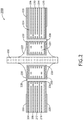
- the circuit card 200 comprises a through-hole pin 202 and a plurality of conductive layers 204, 206, 208, 210, 212, 214, 216, 218 separated by a dielectric 224.
- a solder mask 220 is used to protect the exterior conductive layers 204, 218.
- Solder 222 is then applied to form a metallurgical bond between the through-hole pin 202 and the plated through-hole barrel 226 connecting to certain of the conductive layers 204, 206, 208, 210, 212, 214, 216, 218. It may be appreciated that in at least one embodiment, certain of the conductive layers 204, 206, 208, 210, 212, 214, 216, 218 may not have direct electrical connectivity to the through-hole pin 202 as more fully described herein.
- the conductive circuit pattern of certain conductive layers 204, 206, 208, 210, 212, 214, 216, 218 are set back from the plated through-hole barrel 226 to prevent or reduce contact with the solder, preventing such heat conduction; for example all of the internal conductive layers 206, 208, 210, 212, 214, 216 (all conductive layers except for the top conductive layer 204 and bottom conductive layer 218) may define circuit patterns set back from the plated through-hole barrel 226. Setting the internal conductive layers 206, 208, 210, 212, 214, 216 may reduce electrical connectivity to the through-hole pin 202, which is traditionally required for power.
- a plurality of vias 228 are disposed around the through-hole pin 202 to provide substantially the same cross-sectional area for electrical connectivity between the conductive layers 206, 208, 210, 212, 214, 216.
- ground plane portions 230 may be at different distances from the through-hole pin.
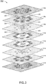
- the circuit card 300 comprises a plurality of conductive layers 304, 306, 308, 310, 312, 314, 316.
- the conductive layers 304, 306, 308, 310, 312, 314, 316, 318 each define a through-hole which may receive a through-hole pin 302.
- the circuit card 300 comprises a top through-hole connection layer 304 and corresponding bottom through-hole connection layer 318; an upper outer ground layer 306 and lower outer ground layer 316; an upper parallel connection layer 308 and lower parallel connection layer 314; and an upper internal ground layer 310 and lower internal ground layer 312.
- the circuit card 300 also includes any number of internal layers between the upper internal ground layer 310 and lower internal ground layer 312.
- the circuit card 300 includes any number of internal ground layers 310, 312.
- electrical connectivity only exists in the top through-hole connection layer 304 and bottom through-hole connection layer 318.
- Internal conductive layers 306, 308, 310, 312, 314, 316 may be electrically isolated from the central through-hole via a barrel 322 and through-hole pin 302.
- the internal conductive layers 306, 308, 310, 312, 314, 316 create a high thermal resistance from the barrel 322 of the through-hole pin 302 connection to the circuit card 300. Available paths for heat transfer away from the through-hole barrel 322 are thereby minimized.
- Internal conductive layers 306, 308, 310, 312, 314, 316 may have additional clearance from the through-hole pin 302 to provide increased thermal resistance.
- ground layers 306, 316 include the only internal copper features that approach the through-hole pin 302. Such ground layers 306, 316 provide a path for return current while maintaining a low inductance connection and minimizing the electrical loop area. Such return path may facilitate a reduced risk of EMI qualification failures.
- a circuit card 300 improves solderability by insulating the through-hole such that heat transfer to the through-hole pin 302 is maximized while heat transfer to the adjacent internal conductive layers 306, 308, 310, 312, 314, 316 is minimized.
- the insulation restricts and guides heat flow during soldering to the areas of the via structure where the heat is needed to provide more efficient heat transfer and improved soldering performance of the through-hole pin 302.
- vias 320 are placed around the circumference of the through-hole pin 302 to connect additional internal conductive layers 306, 308, 310, 312, 314, 316 without connecting directly to the central through-hole plated barrel 322 on inner layers.
- the vias 320 provide paths to other conductive layers 304, 306, 308, 310, 312, 314, 316, 318 for reduced impedance of parallel copper shapes or planes allowing for improved electrical performance.
- Vias 320 may be buried, blind, microvia, etc.
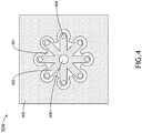
- top circuit card layer 304 (also applicable to a bottom circuit card layer 318 in FIG. 3 ) according to an exemplary embodiment of the concepts disclosed herein is shown.
- the top circuit card layer 304 includes a conductive layer 400 disposed on a non-conductive substrate.
- the top circuit card layer 400 defines a through-hole 406 for receiving a through-hole pin.
- a setback region 404 separates the through-hole from the conductive layer 400.
- the setback region 404 may be approximately thirty thousandths of an inch ( ⁇ 40 mil) or 0.76 millimeters.
- the top circuit card layer 304 can contact a soldering iron directly for conduction.
- the top circuit card layer 304 defines a plurality of via through-holes 408 disposed around the through-hole for receiving a corresponding via fill material.
- the vias provide electrical connectivity to other layers in the circuit card and allow layers to be placed in parallel.
- a cross-pattern of traces 402 connect the vias to the through-hole pin.
- Such traces 402 may provide the only connection from the through-hole pin to conductive layers of other layers in the circuit card by way of the vias.
- the setback region 404 allows soldering iron heat to be applied directly to the top circuit card layer 304.
- the cross-pattern traces 402 to vias minimizes heat transfer away from the through-hole 406.
- the bottom circuit card layer (318 in FIG. 3 ) is substantially identical to a top circuit card layer 304.
- the setback region may be approximately thirty thousandths of an inch ( ⁇ 30 mil) or 0.76 millimeters, and may contact a soldering iron directly for conduction.
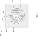
- FIG. 5 a top view of a circuit card ground layer 306 (also 316 in FIG. 3 ) according to an exemplary embodiment of the concepts disclosed herein is shown.
- the circuit card ground layer 306 includes a conductive layer 500 disposed on a non-conductive substrate.
- the circuit card ground layer 306 defines a through-hole 512 for receiving a through-hole pin.
- a setback region 508 separates the through-hole 512 from the conductive layer 500.
- a through-hole barrel 510 may line the through-hole 512.
- the setback region 508 is less than similar setback regions of other layers; that is to say, the conductive layer 500 of the circuit card ground layer 306 is closer to the through-hole 512 than any other layer in the circuit card.
- the small setback region 508 in the circuit card ground layer 306 maintains low inductance and a very small electrical loop area for high frequency currents, which may facilitate a reduced risk of EMI qualification failures.
- the through-hole 512 is plated with a through-hole barrel 514.
- the circuit card ground layer 306 defines a plurality of via through-holes 506 disposed around the through-hole 512 for receiving a corresponding via filler material.
- the vias provide electrical connectivity to other layers in the circuit card and allow layers to be placed in parallel.
- the via through-holes 506 are plated with a via barrel 504.
- the conductive layer 500 defines a via set back region 502 from each via.
- the circuit card includes an upper circuit card ground layer 306 directly beneath a top circuit card layer and a lower circuit card ground layer (316 in FIG. 3 ) directly above a bottom circuit card layer.
- FIG. 6 a top view of a circuit card inner power plane layer 308 (also 314 in FIG. 3 ) according to an exemplary embodiment of the concepts disclosed herein is shown.
- the inner power plane layer 308 includes a conductive layer 600 disposed on a non-conductive substrate.
- the inner power plane layer 308 defines a through-hole 608 for receiving a through-hole pin.
- a setback region 606 separates the through-hole 608 from the conductive layer 600.
- a through-hole barrel 610 may line the through-hole 608.
- the inner power plane layer 308 defines a plurality of via through-holes 604 disposed around the through-hole 608 for receiving a corresponding via filler material.
- the vias provide electrical connectivity to other layers in the circuit card and allow layers to be placed in parallel.
- the setback region 606 completely isolates the through-hole 610 from the conductive layer 600 such that the circuit card inner power plane layer 308 only connects to the vias.
- the setback region 606 provides increased thermal resistance to the through-hole 608.
- the conductive layer 600 and vias provide for low electrical impedance.
- the circuit card includes an upper inner power plane layer 308 directly beneath an upper circuit card ground layer and a lower inner power plane layer (314 in FIG. 3 ) directly above a lower circuit card ground layer.
- the circuit card includes any number of internal power layers disposed between an upper circuit card ground layer and a lower circuit card ground layer.
- FIG. 7 a top view of a circuit card internal ground layer 310 (also 312 in FIG. 3 ) according to an exemplary embodiment of the concepts disclosed herein is shown.
- the internal ground layer 310 includes a conductive layer 700 disposed on a non-conductive substrate.
- the internal ground layer 310 defines a through-hole 710 for receiving a through-hole pin.
- a setback region 702 separates the through-hole 710 from the conductive layer 700.
- a through-hole barrel 708 may line the through-hole 710.
- the internal ground layer 310 defines a plurality of via through-holes 706 disposed around the through-hole 710 for receiving a corresponding via filler material.
- the vias provide electrical connectivity to other layers in the circuit card and allow layers to be placed in parallel.
- the setback region 702 extends to the edge of the vias. The setback region 702 maximizes thermal resistance to the through-hole pin while allowing electrical connectivity to the vias.
- the via through-holes 706 are plated with a via barrel 704.
- the circuit card includes any number of internal ground layers 310 disposed between an upper circuit card ground layer and a lower circuit card ground layer.
- FIG. 8 a side, cross-sectional view of a circuit card 800 according to an exemplary embodiment of the concepts disclosed herein is shown.
- the circuit card 800 comprises a surface mounted connector 802 and a plurality of conductive layers 804, 806, 808, 810, 812, 814, 816, 818 separated by a dielectric 824.
- a solder mask 820 is used to protect the exterior conductive layers 804, 818.
- Solder 822 is then applied to form a metallurgical bond between the surface mounted connector 802 and top circuit card layer 804.
- the conductive circuit pattern of certain conductive layers 804, 806, 808, 810, 812, 814, 816, 818 are set back from any solder proximal regions; for example all of the internal conductive layers 806, 808, 810, 812, 814, 816 (all conductive layers except for the top conductive layer 804 and bottom conductive layer 818) may define circuit patterns set back from the solder proximal regions. Setting back the internal conductive layers 806, 808, 810, 812, 814, 816 may reduce electrical connectivity to the through-hole pin 802, which is traditionally required for power.
- a plurality of vias 826 are disposed around the surface mounted connector 802 to provide substantially the same cross-sectional area for electrical connectivity between the conductive layers 806, 808, 810, 812, 814, 816.
- ground plane portions 830 may be at different distances from the through-hole pin.
- Circuit card production processes utilizing embodiments of the present disclosure may produce less scrap and may be easier to rework. Such embodiments allow for improved solder fill, and therefore higher quality circuit cards.
- the inventive concepts disclosed herein may be extended to other circuit card assemblies with similar through-hole component terminations.
- embodiments of the present disclosure may utilize lead free solder as may be mandated by environmental regulations.
- circuit card elements not specifically discussed are envisioned.
- circuit cards with signal layers having a conductive layer setback may be included.
- Circuit traces for signals may reside on layers between ground and power planes.
Landscapes
- Engineering & Computer Science (AREA)
- Microelectronics & Electronic Packaging (AREA)
- Structure Of Printed Boards (AREA)
- Production Of Multi-Layered Print Wiring Board (AREA)
Abstract
Description
- The present application claims priority to
U.S. Provisional App. No. 63/025,757 (filed May 15, 2020 - Large through-hole or surface mount leaded components typically utilized in power supply technology such as transformers and inductors are difficult to solder or re-work in a factory environment.
- Such components often require additional solder processing steps such as pre-heating; they can lack appropriate solder fill as defined in industry acceptance standards to meet electrical and mechanical performance characteristics; and re-work is difficult or impossible without excess scrap due to circuit card copper content, laminate stack-up, and internal circuit card layer solder connections. Furthermore, higher soldering temperatures leads to integrity issues at the plated through-hole, delamination, decomposition, and layer separation. Copper dissolution may result from extended soldering times.
- These components require specialized soldering equipment such as specialty irons and soldering tips, selective solder machines, solder pots, hotplates/pre-heaters, etc. Furthermore, lead-free solder alloys with higher melting points than traditional tin-lead solders create further difficulties maintaining the high temperatures necessary to get the solder to flow into the plated through-holes or onto the surface mount conductor surfaces. Rework/repair of these devices becomes almost an impossible task. These issues will become more pronounced as the industry trends toward higher power density and lead-free materials.
- High temperatures and long soldering dwell times lead to an increased risk of PCB integrity issues affecting long term reliability. PCB material defects such as laminate delamination, thermal decomposition, pad lifting, inner layer separation and copper dissolution are all possible outcomes if the soldering process is not controlled.
- In one aspect, embodiments of the inventive concepts disclosed herein are directed to a system of circuit card components with through-hole electrical connections for soldering having recessed copper layers for thermal insulation. Thermal insulation prevents heat conduction away from flowing solder, allowing the solder to flow freely through the through-hole and around the pin to be soldered. Even high-temperature, lead-free solders may maintain the necessary temperature to flow more efficiently. Different circuit layers include specialized features based on distance from a top or bottom surface and the specific plane layers (ground, power).
- In a further aspect, vias surrounding the through-hole maintain the necessary cross-sectional area for electrical connectivity.
- The embodiments of the inventive concepts disclosed apply to both axial as well as surface mounted devices. Surface mount devices oftentimes contain many vias within the surface mount pad pattern that also cause heat to flow from the solder joint.
- It is to be understood that both the foregoing general description and the following detailed description are exemplary and explanatory only and should not restrict the scope of the claims. The accompanying drawings, which are incorporated in and constitute a part of the specification, illustrate exemplary embodiments of the inventive concepts disclosed herein and together with the general description, serve to explain the principles.
- The numerous advantages of the embodiments of the inventive concepts disclosed herein may be better understood by those skilled in the art by reference to the accompanying figures in which:
- FIG. 1
- shows a side, cross-sectional view of a state-of-the-art circuit card;
- FIG. 2
- shows a side, cross-sectional view of a circuit card according to an exemplary embodiment of the concepts disclosed herein;
- FIG. 3
- shows an orthogonal, exploded view of a circuit card according to an exemplary embodiment of the concepts disclosed herein;
- FIG. 4
- shows a top view of a circuit card layer according to an exemplary embodiment of the concepts disclosed herein;
- FIG. 5
- shows a top view of a circuit card layer according to an exemplary embodiment of the concepts disclosed herein;
- FIG. 6
- shows a top view of a circuit card layer according to an exemplary embodiment of the concepts disclosed herein;
- FIG. 7
- shows a top view of a circuit card layer according to an exemplary embodiment of the concepts disclosed herein;
- FIG. 8
- shows a side, cross-sectional view of a circuit card according to an exemplary embodiment of the concepts disclosed herein;
- Before explaining at least one embodiment of the inventive concepts disclosed herein in detail, it is to be understood that the inventive concepts are not limited in their application to the details of construction and the arrangement of the components or steps or methodologies set forth in the following description or illustrated in the drawings. In the following detailed description of embodiments of the instant inventive concepts, numerous specific details are set forth in order to provide a more thorough understanding of the inventive concepts. However, it will be apparent to one of ordinary skill in the art having the benefit of the instant disclosure that the inventive concepts disclosed herein may be practiced without these specific details. In other instances, well-known features may not be described in detail to avoid unnecessarily complicating the instant disclosure. The inventive concepts disclosed herein are capable of other embodiments or of being practiced or carried out in various ways. Also, it is to be understood that the phraseology and terminology employed herein is for the purpose of description and should not be regarded as limiting.
- As used herein a letter following a reference numeral is intended to reference an embodiment of the feature or element that may be similar, but not necessarily identical, to a previously described element or feature bearing the same reference numeral (e.g., 1, 1a, 1b). Such shorthand notations are used for purposes of convenience only, and should not be construed to limit the inventive concepts disclosed herein in any way unless expressly stated to the contrary.
- Further, unless expressly stated to the contrary, "or" refers to an inclusive or and not to an exclusive or. For example, a condition A or B is satisfied by anyone of the following: A is true (or present) and B is false (or not present), A is false (or not present) and B is true (or present), and both A and B are true (or present).
- In addition, use of the "a" or "an" are employed to describe elements and components of embodiments of the instant inventive concepts. This is done merely for convenience and to give a general sense of the inventive concepts, and "a" and "an" are intended to include one or at least one and the singular also includes the plural unless it is obvious that it is meant otherwise.
- Finally, as used herein any reference to "one embodiment," or "some embodiments" means that a particular element, feature, structure, or characteristic described in connection with the embodiment is included in at least one embodiment of the inventive concepts disclosed herein. The appearances of the phrase "in some embodiments" in various places in the specification are not necessarily all referring to the same embodiment, and embodiments of the inventive concepts disclosed may include one or more of the features expressly described or inherently present herein, or any combination of sub-combination of two or more such features, along with any other features which may not necessarily be expressly described or inherently present in the instant disclosure.
- Broadly, embodiments of the inventive concepts disclosed herein are directed to a system of circuit card components with through-hole connections for soldering having recessed copper layers to thermal insulation.
- Referring to
FIG. 1 , cross-sectional view of a state-of-the-art circuit card 100 is shown. During the soldering process, asolder mask 120 is applied andmolten solder 122 flows along the surface of the through-hole pin 102 and solders to the barrel of the plated through-hole 126 connecting a plurality ofconductive layers hole pin 102. Theconductive layers dielectric material 124, facilitate heat transfer away from themolten solder 122, causing it to cool. Often, such cooling causes thesolder 122 to solidify before flowing all the way along the through-hole pin 102 creating a weak metallurgical bond to the plated through-hole barrel 126 connecting theconductive layers - Referring to
FIG. 2 , a side, cross-sectional view of acircuit card 200 according to an exemplary embodiment of the concepts disclosed herein is shown. Thecircuit card 200 comprises a through-hole pin 202 and a plurality ofconductive layers solder mask 220 is used to protect the exteriorconductive layers Solder 222 is then applied to form a metallurgical bond between the through-hole pin 202 and the plated through-hole barrel 226 connecting to certain of theconductive layers conductive layers hole pin 202 as more fully described herein. - The conductive circuit pattern of certain
conductive layers hole barrel 226 to prevent or reduce contact with the solder, preventing such heat conduction; for example all of the internalconductive layers conductive layer 204 and bottom conductive layer 218) may define circuit patterns set back from the plated through-hole barrel 226. Setting the internalconductive layers hole pin 202, which is traditionally required for power. In at least one embodiment, a plurality ofvias 228 are disposed around the through-hole pin 202 to provide substantially the same cross-sectional area for electrical connectivity between theconductive layers - Referring to
FIG. 3 , an orthogonal, exploded view of acircuit card 300 according to an exemplary embodiment of the concepts disclosed herein is shown. Thecircuit card 300 comprises a plurality ofconductive layers conductive layers hole pin 302. In at least one embodiment, thecircuit card 300 comprises a top through-hole connection layer 304 and corresponding bottom through-hole connection layer 318; an upperouter ground layer 306 and lowerouter ground layer 316; an upperparallel connection layer 308 and lowerparallel connection layer 314; and an upperinternal ground layer 310 and lowerinternal ground layer 312. In at least one embodiment, thecircuit card 300 also includes any number of internal layers between the upperinternal ground layer 310 and lowerinternal ground layer 312. Alternatively, or in addition, thecircuit card 300 includes any number of internal ground layers 310, 312. - In at least one embodiment, electrical connectivity only exists in the top through-
hole connection layer 304 and bottom through-hole connection layer 318. Internalconductive layers hole pin 302. The internalconductive layers hole pin 302 connection to thecircuit card 300. Available paths for heat transfer away from the through-hole barrel 322 are thereby minimized. Internalconductive layers hole pin 302 to provide increased thermal resistance. - In at least one embodiment, ground layers 306, 316 include the only internal copper features that approach the through-
hole pin 302. Such ground layers 306, 316 provide a path for return current while maintaining a low inductance connection and minimizing the electrical loop area. Such return path may facilitate a reduced risk of EMI qualification failures. - A
circuit card 300 according to the present disclosure improves solderability by insulating the through-hole such that heat transfer to the through-hole pin 302 is maximized while heat transfer to the adjacent internalconductive layers hole pin 302. - In at least one embodiment, vias 320 are placed around the circumference of the through-
hole pin 302 to connect additional internalconductive layers vias 320 provide paths to otherconductive layers Vias 320 may be buried, blind, microvia, etc. - Referring to
FIG. 4 , a top view of a top circuit card layer 304 (also applicable to a bottomcircuit card layer 318 inFIG. 3 ) according to an exemplary embodiment of the concepts disclosed herein is shown. The topcircuit card layer 304 includes aconductive layer 400 disposed on a non-conductive substrate. The topcircuit card layer 400 defines a through-hole 406 for receiving a through-hole pin. - In at least one embodiment, a
setback region 404 separates the through-hole from theconductive layer 400. In at least one embodiment, thesetback region 404 may be approximately thirty thousandths of an inch (∼40 mil) or 0.76 millimeters. The topcircuit card layer 304 can contact a soldering iron directly for conduction. - In at least one embodiment, the top
circuit card layer 304 defines a plurality of via through-holes 408 disposed around the through-hole for receiving a corresponding via fill material. The vias provide electrical connectivity to other layers in the circuit card and allow layers to be placed in parallel. - In at least one embodiment, a cross-pattern of
traces 402 connect the vias to the through-hole pin.Such traces 402 may provide the only connection from the through-hole pin to conductive layers of other layers in the circuit card by way of the vias. - The
setback region 404 allows soldering iron heat to be applied directly to the topcircuit card layer 304. The cross-pattern traces 402 to vias minimizes heat transfer away from the through-hole 406. - In at least one embodiment, the bottom circuit card layer (318 in
FIG. 3 ) is substantially identical to a topcircuit card layer 304. However, it may be appreciated that differences are envisioned; for example, the setback region may be approximately thirty thousandths of an inch (~30 mil) or 0.76 millimeters, and may contact a soldering iron directly for conduction. - Referring to
FIG. 5 , a top view of a circuit card ground layer 306 (also 316 inFIG. 3 ) according to an exemplary embodiment of the concepts disclosed herein is shown. The circuitcard ground layer 306 includes aconductive layer 500 disposed on a non-conductive substrate. The circuitcard ground layer 306 defines a through-hole 512 for receiving a through-hole pin. Asetback region 508 separates the through-hole 512 from theconductive layer 500. In at least one embodiment, a through-hole barrel 510 may line the through-hole 512. - In at least one embodiment, the
setback region 508 is less than similar setback regions of other layers; that is to say, theconductive layer 500 of the circuitcard ground layer 306 is closer to the through-hole 512 than any other layer in the circuit card. Thesmall setback region 508 in the circuitcard ground layer 306 maintains low inductance and a very small electrical loop area for high frequency currents, which may facilitate a reduced risk of EMI qualification failures. In at least one embodiment, the through-hole 512 is plated with a through-hole barrel 514. - In at least one embodiment, the circuit
card ground layer 306 defines a plurality of via through-holes 506 disposed around the through-hole 512 for receiving a corresponding via filler material. The vias provide electrical connectivity to other layers in the circuit card and allow layers to be placed in parallel. In at least one embodiment, the via through-holes 506 are plated with a viabarrel 504. In at least one embodiment, theconductive layer 500 defines a via set backregion 502 from each via. - In at least one embodiment, the circuit card includes an upper circuit
card ground layer 306 directly beneath a top circuit card layer and a lower circuit card ground layer (316 inFIG. 3 ) directly above a bottom circuit card layer. - Referring to
FIG. 6 , a top view of a circuit card inner power plane layer 308 (also 314 inFIG. 3 ) according to an exemplary embodiment of the concepts disclosed herein is shown. The innerpower plane layer 308 includes aconductive layer 600 disposed on a non-conductive substrate. The innerpower plane layer 308 defines a through-hole 608 for receiving a through-hole pin. Asetback region 606 separates the through-hole 608 from theconductive layer 600. In at least one embodiment, a through-hole barrel 610 may line the through-hole 608. - In at least one embodiment, the inner
power plane layer 308 defines a plurality of via through-holes 604 disposed around the through-hole 608 for receiving a corresponding via filler material. The vias provide electrical connectivity to other layers in the circuit card and allow layers to be placed in parallel. In at least one embodiment, thesetback region 606 completely isolates the through-hole 610 from theconductive layer 600 such that the circuit card innerpower plane layer 308 only connects to the vias. Thesetback region 606 provides increased thermal resistance to the through-hole 608. Theconductive layer 600 and vias provide for low electrical impedance. - In at least one embodiment, the circuit card includes an upper inner
power plane layer 308 directly beneath an upper circuit card ground layer and a lower inner power plane layer (314 inFIG. 3 ) directly above a lower circuit card ground layer. - In at least one embodiment, the circuit card includes any number of internal power layers disposed between an upper circuit card ground layer and a lower circuit card ground layer.
- Referring to
FIG. 7 , a top view of a circuit card internal ground layer 310 (also 312 inFIG. 3 ) according to an exemplary embodiment of the concepts disclosed herein is shown. Theinternal ground layer 310 includes aconductive layer 700 disposed on a non-conductive substrate. Theinternal ground layer 310 defines a through-hole 710 for receiving a through-hole pin. Asetback region 702 separates the through-hole 710 from theconductive layer 700. In at least one embodiment, a through-hole barrel 708 may line the through-hole 710. - In at least one embodiment, the
internal ground layer 310 defines a plurality of via through-holes 706 disposed around the through-hole 710 for receiving a corresponding via filler material. The vias provide electrical connectivity to other layers in the circuit card and allow layers to be placed in parallel. In at least one embodiment, thesetback region 702 extends to the edge of the vias. Thesetback region 702 maximizes thermal resistance to the through-hole pin while allowing electrical connectivity to the vias. In at least one embodiment, the via through-holes 706 are plated with a viabarrel 704. - In at least one embodiment, the circuit card includes any number of internal ground layers 310 disposed between an upper circuit card ground layer and a lower circuit card ground layer.
- Referring to
FIG. 8 , a side, cross-sectional view of acircuit card 800 according to an exemplary embodiment of the concepts disclosed herein is shown. Thecircuit card 800 comprises a surface mountedconnector 802 and a plurality ofconductive layers solder mask 820 is used to protect the exteriorconductive layers Solder 822 is then applied to form a metallurgical bond between the surface mountedconnector 802 and topcircuit card layer 804. - The conductive circuit pattern of certain
conductive layers conductive layers conductive layer 804 and bottom conductive layer 818) may define circuit patterns set back from the solder proximal regions. Setting back the internalconductive layers hole pin 802, which is traditionally required for power. In at least one embodiment, a plurality ofvias 826 are disposed around the surface mountedconnector 802 to provide substantially the same cross-sectional area for electrical connectivity between theconductive layers ground plane portions 830 may be at different distances from the through-hole pin. - Circuit card production processes utilizing embodiments of the present disclosure may produce less scrap and may be easier to rework. Such embodiments allow for improved solder fill, and therefore higher quality circuit cards. The inventive concepts disclosed herein may be extended to other circuit card assemblies with similar through-hole component terminations. Furthermore, embodiments of the present disclosure may utilize lead free solder as may be mandated by environmental regulations.
- It may be appreciated that circuit card elements not specifically discussed are envisioned. For example, circuit cards with signal layers having a conductive layer setback may be included. Circuit traces for signals may reside on layers between ground and power planes.
- It is believed that the inventive concepts disclosed herein and many of their attendant advantages will be understood by the foregoing description of embodiments of the inventive concepts disclosed, and it will be apparent that various changes may be made in the form, construction, and arrangement of the components thereof without departing from the broad scope of the inventive concepts disclosed herein or without sacrificing all of their material advantages; and individual features from various embodiments may be combined to arrive at other embodiments. The form herein before described being merely an explanatory embodiment thereof, it is the intention of the following claims to encompass and include such changes. Furthermore, any of the features disclosed in relation to any of the individual embodiments may be incorporated into any other embodiment.
Claims (15)
- A circuit card layer (304;306;308;310;312;314;316;318) comprising:a non-conductive core; anda conductive layer (400) disposed on the non-conductive core,wherein:the circuit card layer defines a surface mount proximal region; andthe conductive layer is set back from the surface mount proximal region sufficient to reduce thermal conduction from a surface mounted connector to the conductive layer during a soldering operation.
- The circuit card layer of Claim 1, wherein the circuit card further defines a plurality of via intersection points, each of the plurality of via intersection points disposed in the conductive layer, and disposed around the surface mount proximal region.
- The circuit card layer of Claim 2, further comprising a plurality of traces (402) disposed on the conductive layer to connect each of a plurality of vias (228,320) disposed in the plurality of via intersection points to in the surface mounted connector at the surface mount proximal region.
- The circuit card layer of Claim 2 or 3, wherein the conductive layer is set back to the via intersection points.
- The circuit card layer of any preceding Claim, wherein the conductive layer is set back at least twenty thousandths of an inch (0.51 mm) from the surface mount proximal region.
- The circuit card layer of any preceding Claim, wherein the circuit card layer comprises a parallel connection layer of a circuit card.
- The circuit card layer of any preceding Claim, wherein the circuit card layer comprises internal ground plane portions (830) defining a return path.
- A circuit card (300) comprising:a plurality of circuit card layers (304;306;308;310;312;314;316;318), each of the plurality of circuit card layers comprising:a non-conductive core; anda conductive layer (400) disposed on the non-conductive core; anda plurality of vias (228,320), each of the plurality of vias intersecting each of the plurality of circuit card layers in a corresponding conductive layer,wherein:each of the plurality of circuit card layers defines a through-hole (126) configured for receiving a through-hole pin (102;202;302);each conductive layer (306-316) is set back from a corresponding through-hole sufficient to insulate a through-hole pin during a soldering operation; andthe plurality of vias are disposed around the through-hole.
- The circuit card of Claim 8, further comprising:a top through-hole connection layer (304) disposed at a top surface of the circuit card,wherein the top through-hole connection layer comprises a plurality of traces connecting the corresponding through-hole connection layer to the plurality of vias.
- The circuit card of Claim 9, wherein the through-hole hole is electrically connected only to the conductive layer of the top through-hole connection layer.
- The circuit card of Claim 9 or 10, further comprising:a bottom through-hole connection layer (318) disposed at a bottom surface of the circuit card,wherein the bottom through-hole connection layer comprises a plurality of traces connecting the corresponding through-hole connection layer to the plurality of vias.
- The circuit card of Claim 11, wherein the through-hole hole is electrically connected only to the conductive layers of the top through-hole connection layer and the bottom through-hole connection layer.
- The circuit card of any of Claims 8 to 12, wherein:a first circuit card layer in the plurality of circuit card layers comprises an upper outer ground layer (306); anda second circuit card layer in the plurality of circuit card layers comprises a lower outer ground layer (316).
- The circuit card of any of Claims 8 to 13, wherein:a first circuit card layer in the plurality of circuit card layers comprises an upper parallel connection layer (308); anda second circuit card layer in the plurality of circuit card layers comprises a lower parallel connection layer (314).
- The circuit card of any of Claims 8 to 14, wherein at least one of the plurality of circuit card layers comprises ground plane portions defining a return path.
Applications Claiming Priority (2)
| Application Number | Priority Date | Filing Date | Title |
|---|---|---|---|
| US202063025757P | 2020-05-15 | 2020-05-15 | |
| US17/319,479 US11570894B2 (en) | 2020-05-15 | 2021-05-13 | Through-hole and surface mount printed circuit card connections for improved power component soldering |
Publications (1)
| Publication Number | Publication Date |
|---|---|
| EP3911128A1 true EP3911128A1 (en) | 2021-11-17 |
Family
ID=76011687
Family Applications (1)
| Application Number | Title | Priority Date | Filing Date |
|---|---|---|---|
| EP21174177.2A Pending EP3911128A1 (en) | 2020-05-15 | 2021-05-17 | Through hole and surface mount printed circuit card connections for improved power component soldering |
Country Status (2)
| Country | Link |
|---|---|
| US (1) | US11570894B2 (en) |
| EP (1) | EP3911128A1 (en) |
Families Citing this family (1)
| Publication number | Priority date | Publication date | Assignee | Title |
|---|---|---|---|---|
| US11876364B2 (en) * | 2022-03-07 | 2024-01-16 | Rolls-Royce Corporation | Multilayer electronic components with soldered through holes |
Citations (7)
| Publication number | Priority date | Publication date | Assignee | Title |
|---|---|---|---|---|
| US5381306A (en) * | 1993-08-20 | 1995-01-10 | Convex Computer Corporation | Method and apparatus for delivering power using a multiplane power via matrix |
| US20040238211A1 (en) * | 2001-04-10 | 2004-12-02 | Yuki Momokawa | Circuit board, circuit board mounting method, and electronic device using the circuit board |
| US20070029108A1 (en) * | 2005-08-05 | 2007-02-08 | Panasonic Ev Energy Co., Ltd. | Printed circuit board and soldering method and apparatus |
| US20080223611A1 (en) * | 2007-03-14 | 2008-09-18 | Fujitsu Limited | Printed wiring board and electric apparatus |
| US20110024177A1 (en) * | 2009-07-29 | 2011-02-03 | Inventec Corporation | Method for soldering electronic components of circuit board and circuit board structure thereof |
| US20110094788A1 (en) * | 2009-10-28 | 2011-04-28 | Ambit Microsystems (Shanghai) Ltd. | Printed circuit board with insulating areas |
| US20190132952A1 (en) * | 2016-03-31 | 2019-05-02 | Fdk Corporation | Multilayer circuit board |
Family Cites Families (14)
| Publication number | Priority date | Publication date | Assignee | Title |
|---|---|---|---|---|
| US6362438B1 (en) | 1999-12-15 | 2002-03-26 | Intel Corporation | Enhanced plated-through hole and via contact design |
| GB2405533A (en) | 2003-09-01 | 2005-03-02 | Siemens Ag | Printed circuit board having through-hole vias and micro-vias |
| US20050231927A1 (en) | 2004-04-20 | 2005-10-20 | Dell Products L.P. | Method, system and apparatus for controlled impedance at transitional plated-through hole via sites using barrel inductance minimization |
| US7238892B2 (en) * | 2005-07-25 | 2007-07-03 | Hewlett-Packard Development Company, L.P. | Printed circuit board including pads with vacancies |
| JP2007059803A (en) * | 2005-08-26 | 2007-03-08 | Fuji Xerox Co Ltd | Printed circuit board, electronic substrate, and electronic apparatus |
| JP2008135645A (en) | 2006-11-29 | 2008-06-12 | Toshiba Corp | Multilayer printed wiring board and interlayer bonding method of multilayer printed wiring board |
| US7656031B2 (en) | 2007-02-05 | 2010-02-02 | Bridge Semiconductor Corporation | Stackable semiconductor package having metal pin within through hole of package |
| US8319116B2 (en) * | 2009-09-11 | 2012-11-27 | Oracle America, Inc. | Rib reinforcement of plated thru-holes |
| CN102883549A (en) * | 2011-07-15 | 2013-01-16 | 台达电子企业管理(上海)有限公司 | Circuit board with heat collection structure and manufacturing method for circuit board |
| KR101365281B1 (en) * | 2012-09-18 | 2014-02-19 | 삼성전기주식회사 | Via structure having open stub and printed circuit boad having it |
| KR102155740B1 (en) | 2014-02-21 | 2020-09-14 | 엘지이노텍 주식회사 | Printed circuit board and manufacturing method of the same |
| US9418965B1 (en) | 2014-10-27 | 2016-08-16 | Altera Corporation | Embedded interposer with through-hole vias |
| JP7131163B2 (en) * | 2018-07-23 | 2022-09-06 | 株式会社デンソー | Electronic control device and electric power steering device using the same |
| US11057985B2 (en) * | 2019-02-28 | 2021-07-06 | Denso Ten Limited | Printed wiring board |
-
2021
- 2021-05-13 US US17/319,479 patent/US11570894B2/en active Active
- 2021-05-17 EP EP21174177.2A patent/EP3911128A1/en active Pending
Patent Citations (7)
| Publication number | Priority date | Publication date | Assignee | Title |
|---|---|---|---|---|
| US5381306A (en) * | 1993-08-20 | 1995-01-10 | Convex Computer Corporation | Method and apparatus for delivering power using a multiplane power via matrix |
| US20040238211A1 (en) * | 2001-04-10 | 2004-12-02 | Yuki Momokawa | Circuit board, circuit board mounting method, and electronic device using the circuit board |
| US20070029108A1 (en) * | 2005-08-05 | 2007-02-08 | Panasonic Ev Energy Co., Ltd. | Printed circuit board and soldering method and apparatus |
| US20080223611A1 (en) * | 2007-03-14 | 2008-09-18 | Fujitsu Limited | Printed wiring board and electric apparatus |
| US20110024177A1 (en) * | 2009-07-29 | 2011-02-03 | Inventec Corporation | Method for soldering electronic components of circuit board and circuit board structure thereof |
| US20110094788A1 (en) * | 2009-10-28 | 2011-04-28 | Ambit Microsystems (Shanghai) Ltd. | Printed circuit board with insulating areas |
| US20190132952A1 (en) * | 2016-03-31 | 2019-05-02 | Fdk Corporation | Multilayer circuit board |
Also Published As
| Publication number | Publication date |
|---|---|
| US20210360789A1 (en) | 2021-11-18 |
| US11570894B2 (en) | 2023-01-31 |
Similar Documents
| Publication | Publication Date | Title |
|---|---|---|
| US11328855B2 (en) | Coil component and manufacturing method thereof | |
| US7382628B2 (en) | Circuit-component-containing module | |
| US3991347A (en) | Plated-through hole soldering to filter body | |
| US7554040B2 (en) | Printed circuit board and soldering method and apparatus | |
| US5446961A (en) | Method for repairing semiconductor substrates | |
| US6646886B1 (en) | Power connection structure | |
| US20070102490A1 (en) | Circuit board,method of mounting surface mounting component on circuit board, and electronic equipment using the same circuit board | |
| US20110061233A1 (en) | Rib reinforcement of plated thru-holes | |
| JP6696332B2 (en) | Printed board | |
| US6081996A (en) | Through hole circuit board interconnect | |
| US20100236823A1 (en) | Ring of power via | |
| EP1631133B1 (en) | Visually inspectable surface mount device pad | |
| US20070257355A1 (en) | Soldering structure of through hole | |
| GB2422491A (en) | Printed circuit board | |
| US6881906B2 (en) | Printed circuit board comprising a contact sleeve that is mounted thereon | |
| US11570894B2 (en) | Through-hole and surface mount printed circuit card connections for improved power component soldering | |
| US6512185B2 (en) | Printed-wiring board | |
| US20110308847A1 (en) | Method for high-temperature circuit board assembly | |
| US20170290215A1 (en) | Electronic Assemblies without Solder and Methods for their manufacture | |
| AU2019215528B2 (en) | Printed circuit board, manufacturing method for printed circuit board, and mobile terminal | |
| US3535769A (en) | Formation of solder joints across gaps | |
| US10299387B2 (en) | Substrate on which electronic component is soldered, electronic device, method for soldering electronic component | |
| CN117939780A (en) | Circuit board, circuit board assembly and manufacturing method thereof | |
| US10225926B2 (en) | Contact arrangement for a multi-layer circuit board | |
| CN213126630U (en) | Resin substrate and electronic device |
Legal Events
| Date | Code | Title | Description |
|---|---|---|---|
| PUAI | Public reference made under article 153(3) epc to a published international application that has entered the european phase |
Free format text: ORIGINAL CODE: 0009012 |
|
| STAA | Information on the status of an ep patent application or granted ep patent |
Free format text: STATUS: THE APPLICATION HAS BEEN PUBLISHED |
|
| AK | Designated contracting states |
Kind code of ref document: A1 Designated state(s): AL AT BE BG CH CY CZ DE DK EE ES FI FR GB GR HR HU IE IS IT LI LT LU LV MC MK MT NL NO PL PT RO RS SE SI SK SM TR |
|
| B565 | Issuance of search results under rule 164(2) epc |
Effective date: 20211020 |
|
| STAA | Information on the status of an ep patent application or granted ep patent |
Free format text: STATUS: REQUEST FOR EXAMINATION WAS MADE |
|
| 17P | Request for examination filed |
Effective date: 20220517 |
|
| RBV | Designated contracting states (corrected) |
Designated state(s): AL AT BE BG CH CY CZ DE DK EE ES FI FR GB GR HR HU IE IS IT LI LT LU LV MC MK MT NL NO PL PT RO RS SE SI SK SM TR |
|
| STAA | Information on the status of an ep patent application or granted ep patent |
Free format text: STATUS: EXAMINATION IS IN PROGRESS |
|
| 17Q | First examination report despatched |
Effective date: 20240305 |