EP3910799A1 - Phase-locked loop circuit and digital-to-time convertor error cancelation method thereof - Google Patents
Phase-locked loop circuit and digital-to-time convertor error cancelation method thereof Download PDFInfo
- Publication number
- EP3910799A1 EP3910799A1 EP21173762.2A EP21173762A EP3910799A1 EP 3910799 A1 EP3910799 A1 EP 3910799A1 EP 21173762 A EP21173762 A EP 21173762A EP 3910799 A1 EP3910799 A1 EP 3910799A1
- Authority
- EP
- European Patent Office
- Prior art keywords
- dtc
- signal
- output
- selection circuit
- selection
- Prior art date
- Legal status (The legal status is an assumption and is not a legal conclusion. Google has not performed a legal analysis and makes no representation as to the accuracy of the status listed.)
- Granted
Links
Images




Classifications
-
- H—ELECTRICITY
- H03—ELECTRONIC CIRCUITRY
- H03L—AUTOMATIC CONTROL, STARTING, SYNCHRONISATION OR STABILISATION OF GENERATORS OF ELECTRONIC OSCILLATIONS OR PULSES
- H03L7/00—Automatic control of frequency or phase; Synchronisation
- H03L7/06—Automatic control of frequency or phase; Synchronisation using a reference signal applied to a frequency- or phase-locked loop
- H03L7/08—Details of the phase-locked loop
-
- H—ELECTRICITY
- H03—ELECTRONIC CIRCUITRY
- H03L—AUTOMATIC CONTROL, STARTING, SYNCHRONISATION OR STABILISATION OF GENERATORS OF ELECTRONIC OSCILLATIONS OR PULSES
- H03L7/00—Automatic control of frequency or phase; Synchronisation
- H03L7/06—Automatic control of frequency or phase; Synchronisation using a reference signal applied to a frequency- or phase-locked loop
- H03L7/08—Details of the phase-locked loop
- H03L7/081—Details of the phase-locked loop provided with an additional controlled phase shifter
-
- H—ELECTRICITY
- H03—ELECTRONIC CIRCUITRY
- H03L—AUTOMATIC CONTROL, STARTING, SYNCHRONISATION OR STABILISATION OF GENERATORS OF ELECTRONIC OSCILLATIONS OR PULSES
- H03L7/00—Automatic control of frequency or phase; Synchronisation
- H03L7/06—Automatic control of frequency or phase; Synchronisation using a reference signal applied to a frequency- or phase-locked loop
- H03L7/08—Details of the phase-locked loop
- H03L7/085—Details of the phase-locked loop concerning mainly the frequency- or phase-detection arrangement including the filtering or amplification of its output signal
- H03L7/087—Details of the phase-locked loop concerning mainly the frequency- or phase-detection arrangement including the filtering or amplification of its output signal using at least two phase detectors or a frequency and phase detector in the loop
-
- G—PHYSICS
- G04—HOROLOGY
- G04F—TIME-INTERVAL MEASURING
- G04F10/00—Apparatus for measuring unknown time intervals by electric means
- G04F10/005—Time-to-digital converters [TDC]
-
- H—ELECTRICITY
- H03—ELECTRONIC CIRCUITRY
- H03L—AUTOMATIC CONTROL, STARTING, SYNCHRONISATION OR STABILISATION OF GENERATORS OF ELECTRONIC OSCILLATIONS OR PULSES
- H03L7/00—Automatic control of frequency or phase; Synchronisation
- H03L7/06—Automatic control of frequency or phase; Synchronisation using a reference signal applied to a frequency- or phase-locked loop
- H03L7/08—Details of the phase-locked loop
- H03L7/085—Details of the phase-locked loop concerning mainly the frequency- or phase-detection arrangement including the filtering or amplification of its output signal
Definitions
- the invention generally relates to digital-to-time convertor (DTC) technology, and more particularly, to DTC error cancellation technology in which a reference signal and a feedback signal can be alternately transmitted to the DTC.
- DTC digital-to-time convertor
- a digital-to-time convertor is applied to the Phase-Locked Loop (PLL) circuit, e.g. an all-digital phase-locked loop (ADPLL).
- the DTC can be used to delay the incoming signal (e.g. a reference signal) edges according to the delay control signal at its input.
- the DTC error term may be generated. The DTC error may lead to the mismatch and low-frequency noise in the PLL circuit.
- a phase-locked loop (PLL) circuit and digital-to-time convertor (DTC) error cancelation method are provided to overcome the problems mentioned above.
- An embodiment of the invention provides a PLL circuit.
- the PLL circuit comprises a first DTC, a first selection circuit, and a second selection circuit.
- the first DTC receives a first delay control signal to dither a reference signal or a feedback signal.
- the first selection circuit is coupled to the first DTC.
- the first selection circuit receives the reference signal and the feedback signal, and according to the selection signal, transmits the reference signal or the feedback signal to the first DTC.
- the second selection circuit is coupled to the first DTC and the first selection circuit. The second selection circuit determines the output paths of an output reference signal or an output feedback signal according to the selection signal.
- the first selection circuit comprises a first multiplexer and a second multiplexer
- the second selection circuit comprises a third multiplexer and a fourth multiplexer
- the first selection circuit comprises a first switch and a second switch
- the second selection circuit comprises a third switch and a fourth switch
- the selection signal in a first cycle, is a first value, and the first selection circuit transmits the reference signal to the first DTC and transmits the feedback signal to the second selection circuit.
- the selection signal is a second value, and the first selection circuit transmits the feedback signal to the first DTC and transmits the reference signal to the second selection circuit.
- the second selection circuit outputs the output reference signal based on its first input from the first DTC and outputs the output feedback signal based on its second input from the first selection circuit; and in the second cycle, the second selection circuit outputs the output feedback signal based on its first input from the first DTC and outputs the output reference signal based on its second input from the first selection circuit.
- the PLL circuit further comprises a second DTC.
- the second DTC is coupled to the first selection circuit and the second selection circuit.
- the second DTC receives a second delay control signal to dither the reference signal or the feedback signal.
- the first selection circuit transmits the reference signal or the feedback signal to the second DTC.
- the second selection circuit determines to output the output reference signal based on its first input from the first DTC and output the output feedback signal based on its second input from the second DTC, or to output the output feedback signal based on its first input from the first DTC and output the output reference signal based on its second input from the second DTC.
- the second selection circuit transmits the output reference signal and the output feedback signal to a phase-frequency detector (PFD) or a time-to-digital convertor (TDC).
- PFD phase-frequency detector
- TDC time-to-digital convertor
- a PFD is configured between the first TDC and the second selection circuit.
- a PFD is coupled to the first selection circuit and the PFD is configured in the front of the first selection circuit.
- An embodiment of the invention provides a digital-to-time convertor (DTC) error cancelation method.
- the DTC error cancelation method is applied to a PLL circuit.
- the DTC error cancelation method comprises the steps of using a first selection circuit of the PLL circuit to receive a reference signal and a feedback signal; using the first selection circuit to transmit the reference signal or the feedback signal to a first DTC of the PLL circuit according to the selection signal; using the first DTC to dither the reference signal or the feedback signal according to a first delay control signal; and using a second selection circuit of the PLL circuit to determine the output paths of an output reference signal or an output feedback signal according to the selection signal.
- DTC digital-to-time convertor
- the present invention can remove or reduce DTC non-ideal error or in-band dither noise without digital calibration. More specifically, the noise phase existed on the reference signal path can be copied or duplicated to the feedback signal path, and then cancel each other in the following stage of the PLL (e.g. by TDC or LPF of the PLL).
- the first delay control signal and the second delay control signal are proposed to keep the same setting (e.g. the same DTC code) for two consecutive cycles to make sure the same error/noise is applied to the reference signal path and the feedback signal path.
- FIG. 1 is a block diagram of a phase-locked loop (PLL) circuit 100 according to an embodiment of the invention.
- the PLL circuit 100 may be applied to an all-digital phase-locked loop (ADPLL), but the invention should not be limited thereto.
- the PLL circuit 100 may comprise a first selection circuit 110, a first DTC 120 and a second selection circuit 130.
- FIG. 1 presents a simplified block diagram in which only the elements relevant to the invention are shown. However, the invention should not be limited to what is shown in FIG. 1 .
- the PLL circuit 100 may also comprise other elements.
- the PLL circuit 100 may further comprise a phase-frequency detector (PFD), a time-to-digital convertor (TDC), a divider, a voltage-controlled oscillator (VCO), a lowpass filter (LPF), and so on, but the invention should not limited thereto.
- PFD phase-frequency detector
- TDC time-to-digital convertor
- VCO voltage-controlled oscillator
- LPF lowpass filter
- the first selection circuit 110 may receive a reference signal CK IN_REF , a feedback signal CK IN_FB and a selection signal S SEL .
- the reference signal CK IN_REF is an input reference signal.
- the feedback signal CK IN_FB is fed back from a voltage-controlled oscillator (VCO) (not shown in figures) of the PLL circuit 100.
- the feedback signal CK IN_FB is fed back from a divider (not shown in figures) which is configured between the first selection circuit 110 and a VCO in the PLL circuit 100.
- the first selection circuit 110 may determine to transmit the reference signal CK IN_REF or the feedback signal CK IN_FB to the first DTC 120 according to the selection signal S SEL . If the first selection circuit 110 determines to transmit the reference signal CK IN_REF to the first DTC 120 according to the selection signal S SEL , the first selection circuit 110 may transmit the feedback signal CK IN_FB to the second selection circuit 130. If the first selection circuit 110 determines to transmit the feedback signal CK IN_FB to the first DTC 120 according to the selection signal S SEL , the first selection circuit 110 may transmit the reference signal CK IN_REF to the second selection circuit 130.
- the first DTC 120 may receive a first delay control signal D DTC_1 to dither the reference signal CK IN_REF or the feedback signal CK IN_FB , e.g. the first DTC 120 may delay the edges of the received reference signal CK IN_REF or the received feedback signal CK IN_FB according to the first delay control signal D DTC_1 .
- the value of the first delay control signal D DTC_1 may be kept at least two cycles to ensure the DTC error in first cycle and the DTC error in second cycle can be cancelled out each other. That is to say, if the first delay control signal D DTC_1 needs to be changed, the first delay control signal D DTC_1 has to maintain at least two cycles (e.g.
- the value of the first delay control signal D DTC_1 in the first cycle is the same as the value of the first delay control signal D DTC_1 in the second cycle). Accordingly, if the first delay control signal D DTC_1 needs to be changed again, the first delay control signal D DTC_1 also has to maintain at least two cycles (e.g. the value of the first delay control signal D DTC_1 in the third cycle is the same as the value of the first delay control signal D DTC_1 in the fourth cycle).
- the second selection circuit 130 may determine to couple the output of the first DTC 120 to an output reference port to serve as an output reference signal CK OUT_REF or to an output feedback port to serve as an output feedback signal CK OUT_FB according to the selection signal S SEL . That is to say, the second selection circuit 130 may determine the coupling paths between the first DTC 120, the first selection circuit 110, the output reference port and the output feedback port. If the second selection circuit 130 determines to output its first input (e.g., the output signal from the first DTC 120) as the output reference signal CK OUT_REF , the second selection circuit 130 may further output its second input (e.g., output of the first selection circuit 110) as the output feedback signal CK OUT_FB .
- first input e.g., the output signal from the first DTC 120
- the second selection circuit 130 may further output its second input (e.g., output of the first selection circuit 110) as the output feedback signal CK OUT_FB .
- the second selection circuit 130 may further output its second input (e.g. the output signal from the first selection circuit 110) as the output reference signal CK OUT_REF .
- the second selection circuit 130 may transmit the output reference signal CK OUT_REF and the output feedback signal CK OUT_FB to a phase-frequency detector (PFD) 200 (as shown in FIG. 2 ) of the PLL circuit 100, and then the signals processed by the PFD 200 may be transmitted to a time-to-digital convertor (TDC) (not shown in figures) of the PLL circuit 100.
- the second selection circuit 130 may transmit the output reference signal CK OUT_REF and the output feedback signal CK OUT_FB to the TDC (not shown in figures) of the PLL circuit 100.
- the reference signal CK IN_REF or the feedback signal CK IN_FB can be alternately transmitted to the first DTC 120 with the first selection circuit 110 under control of the selection signal S SEL . Therefore, in the structure of the PLL circuit 100 of FIG. 1 , an extra calibration loop circuit for the first DTC 120 will not need to be configured in the PLL circuit 100 because the DTC error can be cancelled in a lowpass filter (LPF) (not shown in figures) of the PLL circuit 100.
- LPF lowpass filter
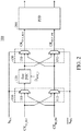
- FIG. 2 is a schematic diagram of PLL circuit 100 according to an embodiment of the invention.
- the first selection circuit 110 may comprise a first multiplexer (MUX) 111 and a second MUX 112
- the second selection circuit 130 may comprise a third MUX 131 and a fourth MUX 132.
- the first MUX 111 and the third MUX 131 may receive the selection signal S SEL and the second MUX 112 and the fourth MUX 132 may receive the inverse selection signal S SEL .
- the first MUX 111 may determine to transmit the reference signal CK IN_REF or the feedback signal CK IN_FB to the first DTC 120 according to the selection signal S SEL .
- the second MUX 112 may determine to transmit the reference signal CK IN_REF or the feedback signal CK IN_FB to the second selection circuit 130 according to the inverse selection signal S SEL .
- the third MUX 131 may determine to output the signal from the first DTC 120 or the second MUX 112 according to the selection signal S SEL .
- the fourth MUX 132 may determine to output the signal from the first DTC 120 or the second MUX 112 according to the inverse selection signal S SEL .
- the third MUX 131 may transmit the output reference signal CK OUT_REF to the PFD 200
- the fourth MUX 132 may transmit the output feedback signal CK OUT_FB to the PFD 200.
- first selection circuit 110 and the second selection circuit 130 are used to illustrate the embodiments of the invention, but the structures of the first selection circuit 110 and the second selection circuit 130 should be limited to FIG. 2 .
- first selection circuit 110 may comprise a first switch and a second switch
- second selection circuit 130 may comprise a third switch and a fourth switch.
- FIG. 3 is a timing diagram of PLL circuit 100 according to an embodiment of the invention.
- the selection signal S SEL in the first cycle, the selection signal S SEL is in a low level and a delay may be occurred in the output reference signal CK OUT_REF . That is to say, taking FIG. 2 for example, in the first cycle, the first MUX 111 of the first selection circuit 110 may transmit the reference signal CK IN_REF to the first DTC 120 according to the selection signal S SEL , and then the first DTC 120 may dither the reference signal CK IN_REF according to the first delay control signal D DTC_1 to generate the output signal that has a delay in response to the reference signal CK IN_REF .
- the third MUX 131 of the second selection circuit 130 may receive the output signal from the first DTC 120 according to the selection signal S SEL and output it as the output reference signal CK OUT_REF to the PFD 200.
- the second MUX 112 of the first selection circuit 110 may receive the feedback signal CK IN_FB and transmit that feedback signal CK IN_FB to the fourth MUX 132 of the second selection circuit 130 according to the inverse selection signal S SEL .
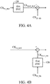
- the fourth MUX 132 may output that feedback signal CK IN_FB as the output feedback signal CK OUT_FB to the PFD 200 according to the inverse selection signal S SEL . Therefore, in the first cycle, the signal diagram of FIG. 2 can be substantially equivalent to the schematic diagram of FIG. 4A .
- the selection signal S SEL is in a high level and a same delay is applied to the first DTC 120. That is to say, in the second cycle, the first MUX 111 of the first selection circuit 110 may transmit the feedback signal CK IN_FB to the first DTC 120 according to the selection signal S SEL , and then the first DTC 120 may dither the feedback signal CK IN_FB according to the first delay control signal D DTC_1 to generate the output signal that has a delay in response to the feedback signal CK IN_FB .
- the delay amount in the second cycle is the same as that in the first cycle since the control signal D DTC_1 keeps the same setting.
- the fourth MUX 132 of the second selection circuit 130 may receive the output signal from the first DTC 120 according to the inverse selection signal S SEL and output it as the output feedback signal CK OUT_FB to the PFD 200.
- the second MUX 112 of the first selection circuit 110 may receive the reference signal CK IN_REF and transmit that reference signal CK IN_REF to the third MUX 131 of the second selection circuit 130 according to the inverse selection signal S SEL .
- the third MUX 131 may output the reference signal CK IN_REF as the output reference signal CK OUT_REF to the PFD 200 according to the selection signal S SEL . Therefore, in the second cycle, the signal diagram of FIG.2 can be substantially equivalent to the schematic diagram of FIG. 4B .
- the first selection circuit 110 may swap the transmission paths of the reference signal CK IN_REF and the feedback signal CK IN_FB in each cycle according to the selection signal S SEL .
- the value of the first delay control signal D DTC_1 may be kept at least two cycles to ensure the DTC error in first cycle and the DTC error in second cycle can be cancelled out each other. It should be noted that the timing diagram of FIG. 3 is only used to illustrate the embodiments of the invention, but the invention should not be limited thereto.
- FIG. 5 is a schematic diagram of PLL circuit 100 according to another embodiment of the invention.
- the PLL circuit 100 may further comprise a second DTC 140.
- the second DTC 140 may receive a second delay control signal D DTC_2 to dither the reference signal CK IN_REF or the feedback signal CK IN_FB , e.g. the second DTC 140 may delay the edges of the reference signal CK IN_REF or the feedback signal CK IN_FB according to the second delay control signal D DTC_2 .
- the value of the second delay control signal D DTC_2 may be kept at least two cycles to ensure the DTC error in first cycle and the DTC error in second cycle can be cancelled out each other. That is to say, if the second delay control signal D DTC_2 needs to be changed, the second delay control signal D DTC_2 has to maintain at least two cycles (e.g. the value of the second delay control signal D DTC_2 in the first cycle is the same as the value of the second delay control signal D DTC_2 in the second cycle). Accordingly, if the second delay control signal D DTC_2 needs to be changed again, the second delay control signal D DTC_2 also has to maintain at least two cycles (e.g.
- the value of the second delay control signal D DTC_2 in the third cycle is the same as the value of the second delay control signal D DTC_2 in the fourth cycle). It should be noted that even the second DTC 140 is configured in the PLL circuit 100, an extra calibration loop circuit for the second DTC 140 will not need to be configured in the PLL circuit 100.
- the first MUX 111 of the first selection circuit 110 may transmit the reference signal CK IN_REF to the first DTC 120 according to the selection signal S SEL , and then the first DTC 120 may dither the reference signal CK IN_REF according to the first delay control signal D DTC_1 to generate the output signal that has a delay in response to the reference signal CK IN_REF . Then, the third MUX 131 of the second selection circuit 130 may receive the output signal from the first DTC 120 according to the selection signal S SEL and output it as the output reference signal CK OUT_REF to the PFD 200.
- the second MUX 112 of the first selection circuit 110 may receive the feedback signal CK IN_FB and transmit that feedback signal CK IN_FB to the second DTC 140 according to the inverse selection signal S SEL , and then the second DTC 140 may dither the feedback signal CK IN_FB according to the second delay control signal D DTC_2 to generate the output signal that has a delay in response to the feedback signal CK IN_FB . Then, the fourth MUX 132 of the second selection circuit 130 may receive the output signal from the second DTC 140 according to the inverse selection signal S SEL and output it as the output feedback signal CK OUT_FB to the PFD 200.
- the first MUX 111 of the first selection circuit 110 may transmit the feedback signal CK IN_FB to the first DTC 120 according to the selection signal S SEL , and then the first DTC 120 may dither the feedback signal CK IN_FB according to the first delay control signal D DTC_1 to generate the output signal that has a delay in response to the feedback signal CK IN_FB .
- the delay amount in the second cycle may be the same as that in the first cycle when the control signal D DTC_1 keeps the same setting.
- the fourth MUX 132 of the second selection circuit 130 may receive the output signal from the first DTC 120 according to the inverse selection signal S SEL and output it as the output feedback signal CK OUT_FB to the PFD 200.
- the second MUX 112 of the first selection circuit 110 may receive the reference signal CK IN_REF and transmit that reference signal CK IN_REF to the second DTC 140 according to the inverse selection signal S SEL , and then the second DTC 140 may dither the reference signal CK IN_REF according to the second delay control signal D DTC_2 to generate the output signal that has a delay in response to the reference signal CK IN_REF .
- the delay amount in the second cycle may be the same as that in the first cycle when the control signal D DTC_2 keeps the same setting.
- the third MUX 131 of the second selection circuit 130 may receive the output signal from the second DTC 140 according to the selection signal S SEL and output it as the output reference signal CK OUT_REF to the PFD 200.
- FIG. 5 is only used to illustrate the embodiments of the invention, but the invention should not be limited thereto.
- Other operations of the PLL circuit 100 of FIG. 5 are similar to the PLL circuit 100 of FIGs. 1 and 2 . Therefore, details will not be illustrated again.
- FIG. 6 is a schematic diagram of PLL circuit 100 according to another embodiment of the invention.
- the PFD 200 may be configured between the first DTC 120 and the second selection circuit 130.
- the PLL circuit 100 of FIG. 6 also can only comprise one DTC.
- the operations of the PLL circuit 100 of FIG. 6 are similar to the PLL circuit 100 of FIGs. 1 , 2 and 5 . Therefore, details will not be illustrated again.
- FIG. 7 is a schematic diagram of PLL circuit 100 according to another embodiment of the invention.
- the PFD 200 may be coupled to the first selection circuit 110 and the PFD 200 is configured in the front of the first selection circuit.
- the PLL circuit 100 of FIG. 6 also can only comprise one DTC.
- the operations of the PLL circuit 100 of FIG. 7 are similar to the PLL circuit 100 of FIGs. 1 , 2 and 5 . Therefore, details will not be illustrated again.
- FIG. 8 is a flow chart illustrating a digital-to-time convertor (DTC) error cancelation method according to an embodiment of the invention.
- the DTC error cancelation method can be applied to the PLL circuit 100.
- a first selection circuit of the PLL circuit 100 receives a reference signal and a feedback signal.
- step S820 the first selection circuit of the PLL circuit 100 transmits the reference signal or the feedback signal to a first DTC of the PLL circuit 100 according to the selection signal.
- step S830 the first DTC of the PLL circuit 100 dithers the reference signal or the feedback signal according to a first delay control signal.
- step S840 a second selection circuit of the PLL circuit 100 determines the output paths of an output reference signal or an output feedback signal according to the selection signal.
- the first selection circuit of the PLL circuit 100 may comprise a first multiplexer and a second multiplexer, and the second selection circuit of the PLL circuit 100 may comprise a third multiplexer and a fourth multiplexer.
- the first selection circuit of the PLL circuit 100 may comprise a first switch and a second switch, and the second selection circuit of the PLL circuit 100 may comprise a third switch and a fourth switch.
- the selection signal in a first cycle, the selection signal is a first value, and the first selection circuit of the PLL circuit 100 may transmit the reference signal to the first DTC of the PLL circuit 100 and transmit the feedback signal to the second selection circuit of the PLL circuit 100.
- the selection signal is a second value, and the first selection circuit of the PLL circuit 100 may transmit the feedback signal to the first DTC of the PLL circuit 100 and transmit the reference signal to the second selection circuit of the PLL circuit 100.
- the second selection circuit of the PLL circuit 100 in the first cycle, the second selection circuit of the PLL circuit 100 may output the output reference signal based on its first input from the first DTC and output the output feedback signal based on its second input from the first selection circuit.
- the second selection circuit of the PLL circuit 100 may output the output feedback signal based on its first input from the first DTC and output the output reference signal based on its second input from the first selection circuit.
- a second DTC of the PLL circuit 100 may receive a second delay control signal to dither the reference signal or the feedback signal. Then, the first selection circuit of the PLL circuit 100 may transmit the reference signal or the feedback signal to the second DTC according to the selection signal. Then, the second selection circuit of the PLL circuit 100 may determine to output the output reference signal based on its first input from the first DTC and output the output feedback signal based on its second input from the second DTC, or to output the output feedback signal based on its first input from the first DTC and output the output reference signal based on its second input from the second DTC according to the selection signal.
- the second selection circuit of the PLL circuit 100 may further transmit the output reference signal and the output feedback signal to a phase-frequency detector (PFD) or a time-to-digital convertor (TDC).
- PFD phase-frequency detector
- TDC time-to-digital convertor
- the PFD is configured between the first TDC and the second selection circuit.
- PFD is coupled to the first selection circuit and the PFD is configured in the front of the first selection circuit.
- the reference signal and the feedback signal can be transmitted to the DTC of the PLL circuit alternately. Therefore, the DTC error can be cancelled in the lowpass filter of the PLL circuit to reduce the mismatch and low-frequency noise.
- the present invention can remove or reduce DTC non-ideal error or in-band dither noise without digital calibration. More specifically, the noise phase existed on the reference signal path can be copied or duplicated to the feedback signal path, and then cancel each other in the following stage of the PLL (e.g. by TDC or LPF of the PLL).
- the first delay control signal and the second delay control signal are proposed to keep the same setting (e.g. the same DTC code) for two consecutive cycles to make sure the same error/noise is applied to the reference signal path and the feedback signal path. As compared to one DTC (e.g.
- the first DTC having two DTCs (e.g. the first DTC and the second DTC) can have a smaller step size for each DTC.
- the first delay control signal and the second delay control signal can be the same or different.
- the first delay control signal can have varying DTC code while the second delay control signal can have a fixed DTC code.
- a software module e.g., including executable instructions and related data
- other data may reside in a data memory such as RAM memory, flash memory, ROM memory, EPROM memory, EEPROM memory, registers, a hard disk, a removable disk, a CD-ROM, or any other form of computer-readable storage medium known in the art.
- a sample storage medium may be coupled to a machine such as, for example, a computer/processor (which may be referred to herein, for convenience, as a "processor”) such that the processor can read information (e.g., code) from and write information to the storage medium.
- a sample storage medium may be integral to the processor.
- the processor and the storage medium may reside in an ASIC.
- the ASIC may reside in user equipment.
- the processor and the storage medium may reside as discrete components in user equipment.
- any suitable computer-program product may comprise a computer-readable medium comprising codes relating to one or more of the aspects of the disclosure.
- a computer program product may comprise packaging materials.
Landscapes
- Physics & Mathematics (AREA)
- General Physics & Mathematics (AREA)
- Stabilization Of Oscillater, Synchronisation, Frequency Synthesizers (AREA)
Abstract
Description
- The invention generally relates to digital-to-time convertor (DTC) technology, and more particularly, to DTC error cancellation technology in which a reference signal and a feedback signal can be alternately transmitted to the DTC.
- A digital-to-time convertor (DTC) is applied to the Phase-Locked Loop (PLL) circuit, e.g. an all-digital phase-locked loop (ADPLL). The DTC can be used to delay the incoming signal (e.g. a reference signal) edges according to the delay control signal at its input. However, as the variance of the pressure, temperature, or voltage, the DTC error term may be generated. The DTC error may lead to the mismatch and low-frequency noise in the PLL circuit.
- A phase-locked loop (PLL) circuit and digital-to-time convertor (DTC) error cancelation method are provided to overcome the problems mentioned above.
- An embodiment of the invention provides a PLL circuit. The PLL circuit comprises a first DTC, a first selection circuit, and a second selection circuit. The first DTC receives a first delay control signal to dither a reference signal or a feedback signal. The first selection circuit is coupled to the first DTC. The first selection circuit receives the reference signal and the feedback signal, and according to the selection signal, transmits the reference signal or the feedback signal to the first DTC. The second selection circuit is coupled to the first DTC and the first selection circuit. The second selection circuit determines the output paths of an output reference signal or an output feedback signal according to the selection signal.
- In some embodiments of the invention, the first selection circuit comprises a first multiplexer and a second multiplexer, and the second selection circuit comprises a third multiplexer and a fourth multiplexer.
- In some embodiments of the invention, the first selection circuit comprises a first switch and a second switch, and the second selection circuit comprises a third switch and a fourth switch.
- In some embodiments of the invention, in a first cycle, the selection signal is a first value, and the first selection circuit transmits the reference signal to the first DTC and transmits the feedback signal to the second selection circuit. In a second cycle, the selection signal is a second value, and the first selection circuit transmits the feedback signal to the first DTC and transmits the reference signal to the second selection circuit. In the first cycle, the second selection circuit outputs the output reference signal based on its first input from the first DTC and outputs the output feedback signal based on its second input from the first selection circuit; and in the second cycle, the second selection circuit outputs the output feedback signal based on its first input from the first DTC and outputs the output reference signal based on its second input from the first selection circuit.
- In some embodiments of the invention, the PLL circuit further comprises a second DTC. The second DTC is coupled to the first selection circuit and the second selection circuit. The second DTC receives a second delay control signal to dither the reference signal or the feedback signal. According to the selection signal, the first selection circuit transmits the reference signal or the feedback signal to the second DTC. According to the selection signal, the second selection circuit determines to output the output reference signal based on its first input from the first DTC and output the output feedback signal based on its second input from the second DTC, or to output the output feedback signal based on its first input from the first DTC and output the output reference signal based on its second input from the second DTC.
- In some embodiments of the invention, the second selection circuit transmits the output reference signal and the output feedback signal to a phase-frequency detector (PFD) or a time-to-digital convertor (TDC).
- In some embodiments of the invention, a PFD is configured between the first TDC and the second selection circuit.
- In some embodiments of the invention, a PFD is coupled to the first selection circuit and the PFD is configured in the front of the first selection circuit.
- An embodiment of the invention provides a digital-to-time convertor (DTC) error cancelation method. The DTC error cancelation method is applied to a PLL circuit. The DTC error cancelation method comprises the steps of using a first selection circuit of the PLL circuit to receive a reference signal and a feedback signal; using the first selection circuit to transmit the reference signal or the feedback signal to a first DTC of the PLL circuit according to the selection signal; using the first DTC to dither the reference signal or the feedback signal according to a first delay control signal; and using a second selection circuit of the PLL circuit to determine the output paths of an output reference signal or an output feedback signal according to the selection signal.
- By alternately swapping the paths for the reference signal and the feedback signal (e.g. alternately applying DTC dithering on the reference signal and the feedback signal), the present invention can remove or reduce DTC non-ideal error or in-band dither noise without digital calibration. More specifically, the noise phase existed on the reference signal path can be copied or duplicated to the feedback signal path, and then cancel each other in the following stage of the PLL (e.g. by TDC or LPF of the PLL). The first delay control signal and the second delay control signal are proposed to keep the same setting (e.g. the same DTC code) for two consecutive cycles to make sure the same error/noise is applied to the reference signal path and the feedback signal path.
- Other aspects and features of the invention will become apparent to those with ordinary skill in the art upon review of the following descriptions of specific embodiments of the PLL circuit and DTC error cancelation method.
- The invention will become more fully understood by referring to the following detailed description with reference to the accompanying drawings, wherein:
-
FIG. 1 is a block diagram of phase-locked loop (PLL)circuit 100 according to an embodiment of the invention; -
FIG. 2 is a schematic diagram ofPLL circuit 100 according to an embodiment of the invention; -
FIG. 3 is a timing diagram ofPLL circuit 100 according to an embodiment of the invention; -
FIG. 4A is a schematic diagram of equivalent paths of the reference signal CKIN_REF and the reference signal CKIN_REF according to an embodiment of the invention; -
FIG. 4B is a schematic diagram of equivalent paths of the reference signal CKIN_REF and the reference signal CKIN_REF according to another embodiment of the invention; -
FIG. 5 is a schematic diagram ofPLL circuit 100 according to another embodiment of the invention; -
FIG. 6 is a schematic diagram ofPLL circuit 100 according to another embodiment of the invention; -
FIG. 7 is a schematic diagram ofPLL circuit 100 according to another embodiment of the invention; and -
FIG. 8 is a flow chart illustrating a DTC error cancelation method according to an embodiment of the invention. - The following description is of the best-contemplated mode of carrying out the invention. This description is made for the purpose of illustrating the general principles of the invention and should not be taken in a limiting sense. The scope of the invention is best determined by reference to the appended claims.
-
FIG. 1 is a block diagram of a phase-locked loop (PLL)circuit 100 according to an embodiment of the invention. In an embodiment of the invention, thePLL circuit 100 may be applied to an all-digital phase-locked loop (ADPLL), but the invention should not be limited thereto. As shown inFIG. 1 , thePLL circuit 100 may comprise afirst selection circuit 110, afirst DTC 120 and asecond selection circuit 130. It should be noted thatFIG. 1 presents a simplified block diagram in which only the elements relevant to the invention are shown. However, the invention should not be limited to what is shown inFIG. 1 . ThePLL circuit 100 may also comprise other elements. For example, thePLL circuit 100 may further comprise a phase-frequency detector (PFD), a time-to-digital convertor (TDC), a divider, a voltage-controlled oscillator (VCO), a lowpass filter (LPF), and so on, but the invention should not limited thereto. - In an embodiment of the invention, the
first selection circuit 110 may receive a reference signal CKIN_REF, a feedback signal CKIN_FB and a selection signal SSEL. The reference signal CKIN_REF is an input reference signal. In an embodiment, the feedback signal CKIN_FB is fed back from a voltage-controlled oscillator (VCO) (not shown in figures) of thePLL circuit 100. In another embodiment, the feedback signal CKIN_FB is fed back from a divider (not shown in figures) which is configured between thefirst selection circuit 110 and a VCO in thePLL circuit 100. In the embodiment, thefirst selection circuit 110 may determine to transmit the reference signal CKIN_REF or the feedback signal CKIN_FB to thefirst DTC 120 according to the selection signal SSEL. If thefirst selection circuit 110 determines to transmit the reference signal CKIN_REF to thefirst DTC 120 according to the selection signal SSEL, thefirst selection circuit 110 may transmit the feedback signal CKIN_FB to thesecond selection circuit 130. If thefirst selection circuit 110 determines to transmit the feedback signal CKIN_FB to thefirst DTC 120 according to the selection signal SSEL, thefirst selection circuit 110 may transmit the reference signal CKIN_REF to thesecond selection circuit 130. - In an embodiment of the invention, the
first DTC 120 may receive a first delay control signal DDTC_1 to dither the reference signal CKIN_REF or the feedback signal CKIN_FB, e.g. thefirst DTC 120 may delay the edges of the received reference signal CKIN_REF or the received feedback signal CKIN_FB according to the first delay control signal DDTC_1. In the embodiment, the value of the first delay control signal DDTC_1 may be kept at least two cycles to ensure the DTC error in first cycle and the DTC error in second cycle can be cancelled out each other. That is to say, if the first delay control signal DDTC_1 needs to be changed, the first delay control signal DDTC_1 has to maintain at least two cycles (e.g. the value of the first delay control signal DDTC_1 in the first cycle is the same as the value of the first delay control signal DDTC_1 in the second cycle). Accordingly, if the first delay control signal DDTC_1 needs to be changed again, the first delay control signal DDTC_1 also has to maintain at least two cycles (e.g. the value of the first delay control signal DDTC_1 in the third cycle is the same as the value of the first delay control signal DDTC_1 in the fourth cycle). - In an embodiment of the invention, the
second selection circuit 130 may determine to couple the output of thefirst DTC 120 to an output reference port to serve as an output reference signal CKOUT_REF or to an output feedback port to serve as an output feedback signal CKOUT_FB according to the selection signal SSEL. That is to say, thesecond selection circuit 130 may determine the coupling paths between thefirst DTC 120, thefirst selection circuit 110, the output reference port and the output feedback port. If thesecond selection circuit 130 determines to output its first input (e.g., the output signal from the first DTC 120) as the output reference signal CKOUT_REF, thesecond selection circuit 130 may further output its second input (e.g., output of the first selection circuit 110) as the output feedback signal CKOUT_FB. If thesecond selection circuit 130 determines to output its first input (e.g., the output signal from the first DTC 120) as the output feedback signal CKOUT_FB, thesecond selection circuit 130 may further output its second input (e.g. the output signal from the first selection circuit 110) as the output reference signal CKOUT_REF. In an embodiment of the invention, thesecond selection circuit 130 may transmit the output reference signal CKOUT_REF and the output feedback signal CKOUT_FB to a phase-frequency detector (PFD) 200 (as shown inFIG. 2 ) of thePLL circuit 100, and then the signals processed by thePFD 200 may be transmitted to a time-to-digital convertor (TDC) (not shown in figures) of thePLL circuit 100. In another embodiment, thesecond selection circuit 130 may transmit the output reference signal CKOUT_REF and the output feedback signal CKOUT_FB to the TDC (not shown in figures) of thePLL circuit 100. - In the structure of the
PLL circuit 100 ofFIG. 1 , the reference signal CKIN_REF or the feedback signal CKIN_FB can be alternately transmitted to thefirst DTC 120 with thefirst selection circuit 110 under control of the selection signal SSEL. Therefore, in the structure of thePLL circuit 100 ofFIG. 1 , an extra calibration loop circuit for thefirst DTC 120 will not need to be configured in thePLL circuit 100 because the DTC error can be cancelled in a lowpass filter (LPF) (not shown in figures) of thePLL circuit 100. -
FIG. 2 is a schematic diagram ofPLL circuit 100 according to an embodiment of the invention. As shown inFIG. 2 , in an embodiment of the invention, thefirst selection circuit 110 may comprise a first multiplexer (MUX) 111 and asecond MUX 112, and thesecond selection circuit 130 may comprise athird MUX 131 and afourth MUX 132. Thefirst MUX 111 and thethird MUX 131 may receive the selection signal SSEL and thesecond MUX 112 and thefourth MUX 132 may receive the inverse selection signalSSEL . Thefirst MUX 111 may determine to transmit the reference signal CKIN_REF or the feedback signal CKIN_FB to thefirst DTC 120 according to the selection signal SSEL. Thesecond MUX 112 may determine to transmit the reference signal CKIN_REF or the feedback signal CKIN_FB to thesecond selection circuit 130 according to the inverse selection signalSSEL . Thethird MUX 131 may determine to output the signal from thefirst DTC 120 or thesecond MUX 112 according to the selection signal SSEL. Thefourth MUX 132 may determine to output the signal from thefirst DTC 120 or thesecond MUX 112 according to the inverse selection signalSSEL . In addition, thethird MUX 131 may transmit the output reference signal CKOUT_REF to thePFD 200, and thefourth MUX 132 may transmit the output feedback signal CKOUT_FB to thePFD 200. - It should be noted that the
first selection circuit 110 and thesecond selection circuit 130 are used to illustrate the embodiments of the invention, but the structures of thefirst selection circuit 110 and thesecond selection circuit 130 should be limited toFIG. 2 . For example, in another embodiment, thefirst selection circuit 110 may comprise a first switch and a second switch, and thesecond selection circuit 130 may comprise a third switch and a fourth switch. -
FIG. 3 is a timing diagram ofPLL circuit 100 according to an embodiment of the invention. As shownFIG. 3 , in the first cycle, the selection signal SSEL is in a low level and a delay may be occurred in the output reference signal CKOUT_REF. That is to say, takingFIG. 2 for example, in the first cycle, thefirst MUX 111 of thefirst selection circuit 110 may transmit the reference signal CKIN_REF to thefirst DTC 120 according to the selection signal SSEL, and then thefirst DTC 120 may dither the reference signal CKIN_REF according to the first delay control signal DDTC_1 to generate the output signal that has a delay in response to the reference signal CKIN_REF. Then, thethird MUX 131 of thesecond selection circuit 130 may receive the output signal from thefirst DTC 120 according to the selection signal SSEL and output it as the output reference signal CKOUT_REF to thePFD 200. In addition, in the first cycle, thesecond MUX 112 of thefirst selection circuit 110 may receive the feedback signal CKIN_FB and transmit that feedback signal CKIN_FB to thefourth MUX 132 of thesecond selection circuit 130 according to the inverse selection signalSSEL . Then, thefourth MUX 132 may output that feedback signal CKIN_FB as the output feedback signal CKOUT_FB to thePFD 200 according to the inverse selection signalSSEL . Therefore, in the first cycle, the signal diagram ofFIG. 2 can be substantially equivalent to the schematic diagram ofFIG. 4A . - In the second cycle, the selection signal SSEL is in a high level and a same delay is applied to the
first DTC 120. That is to say, in the second cycle, thefirst MUX 111 of thefirst selection circuit 110 may transmit the feedback signal CKIN_FB to thefirst DTC 120 according to the selection signal SSEL, and then thefirst DTC 120 may dither the feedback signal CKIN_FB according to the first delay control signal DDTC_1 to generate the output signal that has a delay in response to the feedback signal CKIN_FB. The delay amount in the second cycle is the same as that in the first cycle since the control signal DDTC_1 keeps the same setting. Then, thefourth MUX 132 of thesecond selection circuit 130 may receive the output signal from thefirst DTC 120 according to the inverse selection signalSSEL and output it as the output feedback signal CKOUT_FB to thePFD 200. In addition, in the second cycle, thesecond MUX 112 of thefirst selection circuit 110 may receive the reference signal CKIN_REF and transmit that reference signal CKIN_REF to thethird MUX 131 of thesecond selection circuit 130 according to the inverse selection signalSSEL . Then, thethird MUX 131 may output the reference signal CKIN_REF as the output reference signal CKOUT_REF to thePFD 200 according to the selection signal SSEL. Therefore, in the second cycle, the signal diagram ofFIG.2 can be substantially equivalent to the schematic diagram ofFIG. 4B . - Accordingly, in the third cycle, a second delay (could the same or different to the previous delay value) will be occurred in the output reference signal CKOUT_REF in response to the reference signal CKIN_REF, and in the fourth cycle, the second delay will be occurred in the output feedback signal CKOUT_FB in response to the feedback signal CKIN_FB. Namely, the
first selection circuit 110 may swap the transmission paths of the reference signal CKIN_REF and the feedback signal CKIN_FB in each cycle according to the selection signal SSEL. In addition, in the embodiment, the value of the first delay control signal DDTC_1 may be kept at least two cycles to ensure the DTC error in first cycle and the DTC error in second cycle can be cancelled out each other. It should be noted that the timing diagram ofFIG. 3 is only used to illustrate the embodiments of the invention, but the invention should not be limited thereto. -
FIG. 5 is a schematic diagram ofPLL circuit 100 according to another embodiment of the invention. As shown inFIG. 5 , in an embodiment of the invention, thePLL circuit 100 may further comprise asecond DTC 140. In the embodiment of the invention, thesecond DTC 140 may receive a second delay control signal DDTC_2 to dither the reference signal CKIN_REF or the feedback signal CKIN_FB, e.g. thesecond DTC 140 may delay the edges of the reference signal CKIN_REF or the feedback signal CKIN_FB according to the second delay control signal DDTC_2. In the embodiment, the value of the second delay control signal DDTC_2 may be kept at least two cycles to ensure the DTC error in first cycle and the DTC error in second cycle can be cancelled out each other. That is to say, if the second delay control signal DDTC_2 needs to be changed, the second delay control signal DDTC_2 has to maintain at least two cycles (e.g. the value of the second delay control signal DDTC_2 in the first cycle is the same as the value of the second delay control signal DDTC_2 in the second cycle). Accordingly, if the second delay control signal DDTC_2 needs to be changed again, the second delay control signal DDTC_2 also has to maintain at least two cycles (e.g. the value of the second delay control signal DDTC_2 in the third cycle is the same as the value of the second delay control signal DDTC_2 in the fourth cycle). It should be noted that even thesecond DTC 140 is configured in thePLL circuit 100, an extra calibration loop circuit for thesecond DTC 140 will not need to be configured in thePLL circuit 100. - Taking
FIG. 5 for example, in the first cycle, thefirst MUX 111 of thefirst selection circuit 110 may transmit the reference signal CKIN_REF to thefirst DTC 120 according to the selection signal SSEL, and then thefirst DTC 120 may dither the reference signal CKIN_REF according to the first delay control signal DDTC_1 to generate the output signal that has a delay in response to the reference signal CKIN_REF. Then, thethird MUX 131 of thesecond selection circuit 130 may receive the output signal from thefirst DTC 120 according to the selection signal SSEL and output it as the output reference signal CKOUT_REF to thePFD 200. In addition, in the first cycle, thesecond MUX 112 of thefirst selection circuit 110 may receive the feedback signal CKIN_FB and transmit that feedback signal CKIN_FB to thesecond DTC 140 according to the inverse selection signalSSEL , and then thesecond DTC 140 may dither the feedback signal CKIN_FB according to the second delay control signal DDTC_2 to generate the output signal that has a delay in response to the feedback signal CKIN_FB. Then, thefourth MUX 132 of thesecond selection circuit 130 may receive the output signal from thesecond DTC 140 according to the inverse selection signalSSEL and output it as the output feedback signal CKOUT_FB to thePFD 200. - In the second cycle, the
first MUX 111 of thefirst selection circuit 110 may transmit the feedback signal CKIN_FB to thefirst DTC 120 according to the selection signal SSEL, and then thefirst DTC 120 may dither the feedback signal CKIN_FB according to the first delay control signal DDTC_1 to generate the output signal that has a delay in response to the feedback signal CKIN_FB. The delay amount in the second cycle may be the same as that in the first cycle when the control signal DDTC_1 keeps the same setting. Then, thefourth MUX 132 of thesecond selection circuit 130 may receive the output signal from thefirst DTC 120 according to the inverse selection signalSSEL and output it as the output feedback signal CKOUT_FB to thePFD 200. In addition, in the second cycle, thesecond MUX 112 of thefirst selection circuit 110 may receive the reference signal CKIN_REF and transmit that reference signal CKIN_REF to thesecond DTC 140 according to the inverse selection signalSSEL , and then thesecond DTC 140 may dither the reference signal CKIN_REF according to the second delay control signal DDTC_2 to generate the output signal that has a delay in response to the reference signal CKIN_REF. The delay amount in the second cycle may be the same as that in the first cycle when the control signal DDTC_2 keeps the same setting. Then, thethird MUX 131 of thesecond selection circuit 130 may receive the output signal from thesecond DTC 140 according to the selection signal SSEL and output it as the output reference signal CKOUT_REF to thePFD 200. - It should be noted that the example for
FIG. 5 is only used to illustrate the embodiments of the invention, but the invention should not be limited thereto. Other operations of thePLL circuit 100 ofFIG. 5 are similar to thePLL circuit 100 ofFIGs. 1 and2 . Therefore, details will not be illustrated again. -
FIG. 6 is a schematic diagram ofPLL circuit 100 according to another embodiment of the invention. As shown inFIG. 6 , thePFD 200 may be configured between thefirst DTC 120 and thesecond selection circuit 130. It should be noted that in another embodiment of the invention, thePLL circuit 100 ofFIG. 6 also can only comprise one DTC. The operations of thePLL circuit 100 ofFIG. 6 are similar to thePLL circuit 100 ofFIGs. 1 ,2 and5 . Therefore, details will not be illustrated again. -
FIG. 7 is a schematic diagram ofPLL circuit 100 according to another embodiment of the invention. As shown inFIG. 7 , thePFD 200 may be coupled to thefirst selection circuit 110 and thePFD 200 is configured in the front of the first selection circuit. It should be noted that in another embodiment of the invention, thePLL circuit 100 ofFIG. 6 also can only comprise one DTC. The operations of thePLL circuit 100 ofFIG. 7 are similar to thePLL circuit 100 ofFIGs. 1 ,2 and5 . Therefore, details will not be illustrated again. -
FIG. 8 is a flow chart illustrating a digital-to-time convertor (DTC) error cancelation method according to an embodiment of the invention. The DTC error cancelation method can be applied to thePLL circuit 100. As shown inFIG. 8 , in step S810, a first selection circuit of thePLL circuit 100 receives a reference signal and a feedback signal. - In step S820, the first selection circuit of the
PLL circuit 100 transmits the reference signal or the feedback signal to a first DTC of thePLL circuit 100 according to the selection signal. - In step S830, the first DTC of the
PLL circuit 100 dithers the reference signal or the feedback signal according to a first delay control signal. - In step S840, a second selection circuit of the
PLL circuit 100 determines the output paths of an output reference signal or an output feedback signal according to the selection signal. - In some embodiments, in the DTC error cancelation method, the first selection circuit of the
PLL circuit 100 may comprise a first multiplexer and a second multiplexer, and the second selection circuit of thePLL circuit 100 may comprise a third multiplexer and a fourth multiplexer. - In some embodiments, in the DTC error cancelation method, the first selection circuit of the
PLL circuit 100 may comprise a first switch and a second switch, and the second selection circuit of thePLL circuit 100 may comprise a third switch and a fourth switch. - In some embodiments, in the DTC error cancelation method, in a first cycle, the selection signal is a first value, and the first selection circuit of the
PLL circuit 100 may transmit the reference signal to the first DTC of thePLL circuit 100 and transmit the feedback signal to the second selection circuit of thePLL circuit 100. In a second cycle, the selection signal is a second value, and the first selection circuit of thePLL circuit 100 may transmit the feedback signal to the first DTC of thePLL circuit 100 and transmit the reference signal to the second selection circuit of thePLL circuit 100. Furthermore in the DTC error cancelation method, in the first cycle, the second selection circuit of thePLL circuit 100 may output the output reference signal based on its first input from the first DTC and output the output feedback signal based on its second input from the first selection circuit. In the second cycle, the second selection circuit of thePLL circuit 100 may output the output feedback signal based on its first input from the first DTC and output the output reference signal based on its second input from the first selection circuit. - In some embodiments of the invention, in the DTC error cancelation method, a second DTC of the
PLL circuit 100 may receive a second delay control signal to dither the reference signal or the feedback signal. Then, the first selection circuit of thePLL circuit 100 may transmit the reference signal or the feedback signal to the second DTC according to the selection signal. Then, the second selection circuit of thePLL circuit 100 may determine to output the output reference signal based on its first input from the first DTC and output the output feedback signal based on its second input from the second DTC, or to output the output feedback signal based on its first input from the first DTC and output the output reference signal based on its second input from the second DTC according to the selection signal. - In some embodiments of the invention, in the DTC error cancelation method, the second selection circuit of the
PLL circuit 100 may further transmit the output reference signal and the output feedback signal to a phase-frequency detector (PFD) or a time-to-digital convertor (TDC). In some embodiments of the invention, in the DTC error cancelation method, the PFD is configured between the first TDC and the second selection circuit. In some embodiments of the invention, in the DTC error cancelation method, PFD is coupled to the first selection circuit and the PFD is configured in the front of the first selection circuit. - According to the DTC error cancelation method of the invention, the reference signal and the feedback signal can be transmitted to the DTC of the PLL circuit alternately. Therefore, the DTC error can be cancelled in the lowpass filter of the PLL circuit to reduce the mismatch and low-frequency noise.
- By alternately swapping the paths for the reference signal and the feedback signal (e.g. alternately applying DTC dithering on the reference signal and the feedback signal), the present invention can remove or reduce DTC non-ideal error or in-band dither noise without digital calibration. More specifically, the noise phase existed on the reference signal path can be copied or duplicated to the feedback signal path, and then cancel each other in the following stage of the PLL (e.g. by TDC or LPF of the PLL). The first delay control signal and the second delay control signal are proposed to keep the same setting (e.g. the same DTC code) for two consecutive cycles to make sure the same error/noise is applied to the reference signal path and the feedback signal path. As compared to one DTC (e.g. the first DTC), having two DTCs (e.g. the first DTC and the second DTC) can have a smaller step size for each DTC. However, the first delay control signal and the second delay control signal can be the same or different. For example, the first delay control signal can have varying DTC code while the second delay control signal can have a fixed DTC code.
- Use of ordinal terms such as "first", "second", "third", etc., in the disclosure and claims is for description. It does not by itself connote any order or relationship.
- The steps of the method described in connection with the aspects disclosed herein may be embodied directly in hardware, in a software module executed by a processor, or in a combination of the two. A software module (e.g., including executable instructions and related data) and other data may reside in a data memory such as RAM memory, flash memory, ROM memory, EPROM memory, EEPROM memory, registers, a hard disk, a removable disk, a CD-ROM, or any other form of computer-readable storage medium known in the art. A sample storage medium may be coupled to a machine such as, for example, a computer/processor (which may be referred to herein, for convenience, as a "processor") such that the processor can read information (e.g., code) from and write information to the storage medium. A sample storage medium may be integral to the processor. The processor and the storage medium may reside in an ASIC. The ASIC may reside in user equipment. Alternatively, the processor and the storage medium may reside as discrete components in user equipment. Moreover, in some aspects any suitable computer-program product may comprise a computer-readable medium comprising codes relating to one or more of the aspects of the disclosure. In some aspects a computer program product may comprise packaging materials.
- The above paragraphs describe many aspects. Obviously, the teaching of the invention can be accomplished by many methods, and any specific configurations or functions in the disclosed embodiments only present a representative condition. Those who are skilled in this technology will understand that all of the disclosed aspects in the invention can be applied independently or be incorporated.
- While the invention has been described by way of example and in terms of preferred embodiment, it should be understood that the invention is not limited thereto. Those who are skilled in this technology can still make various alterations and modifications without departing from the scope of this invention. Therefore, the scope of the present invention shall be defined and protected by the following claims and their equivalents.
Claims (16)
- A phase-locked loop (PLL) circuit, comprising:a first DTC (120), for receiving a first delay control signal to dither a reference signal or a feedback signal;a first selection circuit (110), coupled to the first DTC (120), for receiving the reference signal and the feedback signal, and according to a selection signal, transmitting the reference signal or the feedback signal to the first DTC; anda second selection circuit (130), coupled to the first DTC (120) and the first selection circuit (110), according to the selection signal, determining output paths of an output reference signal and an output feedback signal.
- The PLL circuit of claim 1, wherein the first selection circuit comprises a first multiplexer (111) and a second multiplexer (112), and the second selection circuit comprises a third multiplexer (131) and a fourth multiplexer (132), or wherein the first selection circuit comprises a first switch and a second switch, and the second selection circuit comprises a third switch and a fourth switch.
- The PLL circuit of claim 1 or 2, wherein in a first cycle, the selection signal is a first value, the first selection circuit transmits the reference signal to the first DTC; and in a second cycle, the selection signal is a second value, the first selection circuit transmits the feedback signal to the first DTC.
- The PLL circuit of claim 3, wherein in the first cycle, the second selection circuit outputs the output reference signal based on its first input from the first DTC and outputs the output feedback signal based on its second input from the first selection circuit; and in the second cycle, the second selection circuit outputs the output feedback signal based on its first input from the first DTC and outputs the output reference signal based on its second input from the first selection circuit.
- The PLL circuit of claim 3 or 4, wherein the first delay control signal has a same setting during the first cycle and the second cycle.
- The PLL circuit of any one of the preceding claims, further comprising:a second DTC (140), coupled to the first selection circuit and the second selection circuit, for receiving a second delay control signal to dither the reference signal or the feedback signal,wherein according to the selection signal, the first selection circuit transmits the reference signal or the feedback signal to the second DTC, andwherein according to the reference signal, the second selection circuit determines to output the output reference signal based on its first input from the first DTC and output the output feedback signal based on its second input from the second DTC, or to output the output feedback signal based on its first input from the first DTC and output the output reference signal based on its second input from the second DTC according to the selection signal.
- The PLL circuit of claim 6, wherein the second delay control signal has a same setting during the first cycle and the second cycle.
- A digital-to-time convertor (DTC) error cancelation method, applied to a phase-locked loop (PLL) circuit, comprising:receiving, by a first selection circuit (110) of the PLL circuit, a reference signal and a feedback signal;transmitting, by the first selection circuit (110), the reference signal or the feedback signal to a first DTC of the PLL circuit according to a selection signal;dithering, by the first DTC (120), the reference signal or the feedback signal according to a first delay control signal; anddetermining, by a second selection circuit (130) of the PLL circuit, output paths of an output reference signal and an output feedback signal according to the selection signal.
- The DTC error cancelation method of claim 8, wherein the first selection circuit comprises a first multiplexer (110) and a second multiplexer (120), and the second selection circuit comprises a third multiplexer (131) and a fourth multiplexer (132), or wherein the first selection circuit comprises a first switch and a second switch, and the second selection circuit comprises a third switch and a fourth switch.
- The DTC error cancelation method of claim 8 or 9, wherein in a first cycle, the selection signal is a first value, and the method further comprises:
transmitting, by the first selection circuit, the reference signal to the first DTC. - The DTC error cancelation method of claim 10, wherein in a second cycle, the selection signal is a second value, and the method further comprises:
transmitting, by the first selection circuit, the feedback signal to the first DTC. - The DTC error cancelation method of claim 11, wherein in the first cycle, the method further comprises:
outputting, by the second selection circuit, the output reference signal based on its first input from the first DTC and the output feedback signal based on its second input from the first selection circuit. - The DTC error cancelation method of claim 11 or 12, wherein in the second cycle, the method further comprises:
outputting, by the second selection circuit, the output feedback signal based on its first input from the first DTC and the output reference signal based on its second input from the second DTC. - The DTC error cancelation method of claim 11, wherein the first delay control signal has a same setting during the first cycle and the second cycle.
- The DTC error cancelation method of any one of claims 8 to 14, further comprising:receiving, by a second DTC of the PLL circuit, a second delay control signal to dither the reference signal or the feedback signal;transmitting, by the first selection circuit, the reference signal or the feedback signal to the second DTC according to the selection signal; anddetermining, by the second selection circuit, to output the output reference signal based on its first input from the first DTC and output the output feedback signal based on its second input from the second DTC, or to output the output feedback signal based on its first input from the first DTC and output the output reference signal based on its second input from the second DTC according to the selection signal.
- The DTC error cancelation method of claim 15, wherein the second delay control signal has a same setting during the first cycle and the second cycle.
Applications Claiming Priority (2)
| Application Number | Priority Date | Filing Date | Title |
|---|---|---|---|
| US202063024536P | 2020-05-14 | 2020-05-14 | |
| US17/242,395 US11223362B2 (en) | 2020-05-14 | 2021-04-28 | Phase-locked loop circuit and digital-to-time convertor error cancelation method thereof |
Publications (3)
| Publication Number | Publication Date |
|---|---|
| EP3910799A1 true EP3910799A1 (en) | 2021-11-17 |
| EP3910799B1 EP3910799B1 (en) | 2025-11-12 |
| EP3910799B8 EP3910799B8 (en) | 2025-12-24 |
Family
ID=75919254
Family Applications (1)
| Application Number | Title | Priority Date | Filing Date |
|---|---|---|---|
| EP21173762.2A Active EP3910799B8 (en) | 2020-05-14 | 2021-05-13 | Phase-locked loop circuit and digital-to-time convertor error cancelation method thereof |
Country Status (4)
| Country | Link |
|---|---|
| US (1) | US11223362B2 (en) |
| EP (1) | EP3910799B8 (en) |
| CN (1) | CN113676178A (en) |
| TW (1) | TWI764700B (en) |
Families Citing this family (7)
| Publication number | Priority date | Publication date | Assignee | Title |
|---|---|---|---|---|
| US11283437B2 (en) * | 2019-12-17 | 2022-03-22 | Skyworks Solutions, Inc. | Measuring pin-to-pin delays between clock routes |
| EP3996280B1 (en) * | 2020-11-05 | 2025-07-23 | Stichting IMEC Nederland | Circuit and method for random edge injection locking |
| US11387833B1 (en) * | 2021-09-03 | 2022-07-12 | Qualcomm Incorporated | Differential digital-to-time converter for even-order INL cancellation and supply noise/disturbance rejection |
| US11843392B2 (en) * | 2021-12-03 | 2023-12-12 | Texas Instruments Incorporated | Systems and methods for online gain calibration of digital-to-time converters |
| US11916559B2 (en) * | 2021-12-31 | 2024-02-27 | SambaNova Systems, Inc. | Delay-locked loop with widened lock range |
| US12463623B2 (en) | 2022-11-17 | 2025-11-04 | Mediatek Inc. | Phase error compensation circuit and method for compensating phase error between reference clock and feedback clock |
| CN118054784A (en) * | 2022-11-17 | 2024-05-17 | 华为技术有限公司 | Phase-locked loop, noise elimination method, chip and electronic equipment |
Citations (3)
| Publication number | Priority date | Publication date | Assignee | Title |
|---|---|---|---|---|
| US6975695B1 (en) * | 2001-04-30 | 2005-12-13 | Cypress Semiconductor Corp. | Circuit for correction of differential signal path delays in a PLL |
| US20080205551A1 (en) * | 2007-02-28 | 2008-08-28 | Wai Hon Lo | Method, system and apparatus for phase control of transmit diversity signals |
| US20190115926A1 (en) * | 2017-10-13 | 2019-04-18 | Xilinx, Inc. | Dual-path digital-to-time converter |
Family Cites Families (46)
| Publication number | Priority date | Publication date | Assignee | Title |
|---|---|---|---|---|
| US6373301B1 (en) * | 2001-04-18 | 2002-04-16 | Silicon Integrated Systems Corporation | Fast-locking dual rail digital delayed locked loop |
| US7421464B2 (en) * | 2004-09-30 | 2008-09-02 | Motorola, Inc. | System and method for introducing dither for reducing spurs in digital-to-time converter direct digital synthesis |
| US7315215B2 (en) | 2006-03-08 | 2008-01-01 | Motorola,, Inc. | Direct digital synthesizer with variable reference for improved spurious performance |
| US7929929B2 (en) * | 2007-09-25 | 2011-04-19 | Motorola Solutions, Inc. | Method and apparatus for spur reduction in a frequency synthesizer |
| US8098085B2 (en) * | 2009-03-30 | 2012-01-17 | Qualcomm Incorporated | Time-to-digital converter (TDC) with improved resolution |
| EP2339753B1 (en) * | 2009-12-24 | 2012-07-04 | Nxp B.V. | A digital phase locked loop |
| CN103493377B (en) * | 2011-06-01 | 2017-04-26 | 华为技术有限公司 | Spur Suppression in Phase Locked Loops |
| US9077375B2 (en) * | 2011-12-21 | 2015-07-07 | Intel Mobile Communications GmbH | DTC system with high resolution phase alignment |
| US9071304B2 (en) * | 2013-08-16 | 2015-06-30 | Intel IP Corporation | Digital-to-time converter and methods for generating phase-modulated signals |
| US9270288B2 (en) * | 2013-11-27 | 2016-02-23 | Silicon Laboratories Inc. | Time-to-digital converter based on a voltage controlled oscillator |
| EP3035536B1 (en) | 2014-12-19 | 2020-04-29 | Stichting IMEC Nederland | An ADPLL having a TDC circuit with a dynamically adjustable offset delay |
| DE102014119480B4 (en) * | 2014-12-23 | 2018-02-08 | Intel Ip Corp. | Noise shaping circuit, digital-time converter, analog-to-digital converter, digital-to-analog converter, frequency synthesizer, transmitter, receiver, transceiver, method of shaping noise in an input signal |
| US9800141B2 (en) * | 2015-03-10 | 2017-10-24 | Intel IP Corporation | Hysteretic current control with event dithering |
| US9531394B1 (en) | 2015-06-22 | 2016-12-27 | Silicon Laboratories Inc. | Calibration of digital-to-time converter |
| US9362936B1 (en) * | 2015-06-22 | 2016-06-07 | Silicon Laboratories Inc. | Digital-to-time converter |
| US9520890B1 (en) * | 2015-12-23 | 2016-12-13 | Intel IP Corporation | Dual digital to time converter (DTC) based differential correlated double sampling DTC calibration |
| US9740175B2 (en) | 2016-01-18 | 2017-08-22 | Marvell World Trade Ltd. | All-digital phase locked loop (ADPLL) including a digital-to-time converter (DTC) and a sampling time-to-digital converter (TDC) |
| EP3249817B1 (en) * | 2016-05-25 | 2018-12-26 | IMEC vzw | Dtc-based pll and method for operating the dtc-based pll |
| CN107528588A (en) * | 2016-06-21 | 2017-12-29 | 马维尔国际贸易有限公司 | Simulate fractional n phase lock loop |
| US9698807B1 (en) * | 2016-06-30 | 2017-07-04 | Silicon Laboratories Inc. | Time signal conversion using dual time-based digital-to-analog converters |
| US9628262B1 (en) * | 2016-07-19 | 2017-04-18 | Texas Instruments Incorporated | Spur reduction in phase locked loops using reference clock dithering |
| US10158365B2 (en) * | 2016-07-29 | 2018-12-18 | Movellus Circuits, Inc. | Digital, reconfigurable frequency and delay generator with phase measurement |
| US9705512B1 (en) | 2016-09-20 | 2017-07-11 | Realtek Semiconductor Corporation | Self-calibrating fractional-N phase lock loop and method thereof |
| US10886878B2 (en) * | 2016-09-29 | 2021-01-05 | Intel IP Corporation | Modulation circuitry with N.5 division |
| US9941898B1 (en) * | 2016-12-27 | 2018-04-10 | Intel Corporation | Scalable interleaved digital-to-time converter circuit for clock generation |
| US10050634B1 (en) * | 2017-02-10 | 2018-08-14 | Apple Inc. | Quantization noise cancellation for fractional-N phased-locked loop |
| US9979405B1 (en) * | 2017-02-10 | 2018-05-22 | Apple Inc. | Adaptively reconfigurable time-to-digital converter for digital phase-locked loops |
| US10707848B2 (en) * | 2017-03-31 | 2020-07-07 | Apple Inc. | Apparatus and method for interpolating between a first and a second signal |
| US10608603B2 (en) * | 2017-05-16 | 2020-03-31 | Murata Manufacturing Co., Ltd. | Multi-band power amplifier module |
| EP3407497B1 (en) * | 2017-05-22 | 2024-01-17 | Stichting IMEC Nederland | Digital phase-locked loops using digital-to-time converters |
| KR102435034B1 (en) * | 2017-06-21 | 2022-08-23 | 삼성전자주식회사 | Digital phase locked loop and operating method of digital phase locked loop |
| WO2019017864A1 (en) * | 2017-07-17 | 2019-01-24 | Intel IP Corporation | A method and a system for calibrating a phase nonlinearity of a digital-to-time converter |
| EP3701631B8 (en) * | 2017-12-19 | 2022-04-27 | Huawei International Pte. Ltd. | Digital-to-time converter (dtc) assisted all digital phase locked loop (adpll) circuit |
| US10996634B2 (en) * | 2018-01-05 | 2021-05-04 | Samsung Electronics Co., Ltd. | System and method for fast-converging digital-to-time converter (DTC) gain calibration for DTC-based analog fractional-N phase lock loop (PLL) |
| US10581418B2 (en) * | 2018-01-05 | 2020-03-03 | Samsung Electronics Co., Ltd | System and method for fast converging reference clock duty cycle correction for digital to time converter (DTC)-based analog fractional-N phase-locked loop (PLL) |
| KR102527388B1 (en) | 2018-04-06 | 2023-04-28 | 삼성전자주식회사 | Phase locked loop circuit and clock generator comprising digital-to-time convert circuit and operating method thereof |
| US10707879B2 (en) * | 2018-04-13 | 2020-07-07 | KaiKuTek Inc. | Frequency-modulated continuous-wave radar system and frequency tracking method for calibrating frequency gains of a radio frequency signal to approach wideband flatness frequency responses |
| US11545985B2 (en) * | 2018-12-14 | 2023-01-03 | Silicon Laboratories Inc. | Apparatus for digitally controlled oscillators and associated methods |
| CN110061737B (en) * | 2019-04-26 | 2023-05-16 | 海光信息技术股份有限公司 | Phase lock detection output circuit and all-digital phase-locked loop system |
| CN110224697B (en) * | 2019-06-18 | 2022-11-04 | 苏州兆凯电子有限公司 | Phase-locked loop locking method, phase-locked loop circuit and communication transceiving system |
| US10895850B1 (en) * | 2019-07-25 | 2021-01-19 | Si-Ware Systems S.A.E. | Mixed-domain circuit with differential domain-converters |
| CN110391894B (en) * | 2019-08-30 | 2020-08-04 | 清华大学 | Receiving end of synchronous system, synchronous system and particle accelerator |
| US10784872B1 (en) * | 2019-09-17 | 2020-09-22 | Taiwan Semiconductor Manufacturing Company Limited | Fractional realignment techniques for PLLs |
| US10908635B1 (en) * | 2019-12-24 | 2021-02-02 | Silicon Laboratories Inc. | Detection and management of frequency errors in a reference input clock signal |
| US10965297B1 (en) * | 2020-03-03 | 2021-03-30 | Samsung Electronics Co., Ltd | Sigma-delta modulation quantization error reduction technique for fractional-N phase-locked loop (PLL) |
| US11031945B1 (en) * | 2020-09-11 | 2021-06-08 | Apple Inc. | Time-to-digital converter circuit linearity test mechanism |
-
2021
- 2021-04-28 US US17/242,395 patent/US11223362B2/en active Active
- 2021-04-29 TW TW110115536A patent/TWI764700B/en active
- 2021-05-06 CN CN202110492050.6A patent/CN113676178A/en active Pending
- 2021-05-13 EP EP21173762.2A patent/EP3910799B8/en active Active
Patent Citations (3)
| Publication number | Priority date | Publication date | Assignee | Title |
|---|---|---|---|---|
| US6975695B1 (en) * | 2001-04-30 | 2005-12-13 | Cypress Semiconductor Corp. | Circuit for correction of differential signal path delays in a PLL |
| US20080205551A1 (en) * | 2007-02-28 | 2008-08-28 | Wai Hon Lo | Method, system and apparatus for phase control of transmit diversity signals |
| US20190115926A1 (en) * | 2017-10-13 | 2019-04-18 | Xilinx, Inc. | Dual-path digital-to-time converter |
Also Published As
| Publication number | Publication date |
|---|---|
| EP3910799B8 (en) | 2025-12-24 |
| TWI764700B (en) | 2022-05-11 |
| TW202143653A (en) | 2021-11-16 |
| EP3910799B1 (en) | 2025-11-12 |
| US20210359687A1 (en) | 2021-11-18 |
| CN113676178A (en) | 2021-11-19 |
| US11223362B2 (en) | 2022-01-11 |
Similar Documents
| Publication | Publication Date | Title |
|---|---|---|
| US11223362B2 (en) | Phase-locked loop circuit and digital-to-time convertor error cancelation method thereof | |
| EP1148648B1 (en) | Frequency synthesizer | |
| CN101599755B (en) | Clock generation circuit, device for communicating with host, communication system and method for generating output clock signal | |
| US8368435B2 (en) | Method and apparatus for jitter reduction | |
| US7949083B2 (en) | Clock synchroniser | |
| US7541880B2 (en) | Circuit and method for glitch correction | |
| US10587274B2 (en) | Method and system for maintaining a low-jitter low-temperature-drift clock during a holdover operation | |
| JP2002164782A (en) | Clock regenerator and clock signal regenerating method | |
| US20200321969A1 (en) | Phase cancellation in a phase-locked loop | |
| US20090147903A1 (en) | Communication system, receiving apparatus, and receiving method | |
| CN105450218A (en) | Phase tracker for a phase locked loop | |
| US6556086B2 (en) | Fractional-N synthesizer and method of synchronization of the output phase | |
| US20020186087A1 (en) | Data recovery circuit and method thereof | |
| US20150110233A1 (en) | Jitter mitigating phase locked loop circuit | |
| US7760766B2 (en) | Audio processor | |
| US6732286B1 (en) | High latency timing circuit | |
| US7049852B2 (en) | Fractional-integer phase-locked loop system with a fractional-frequency-interval phase frequency detector | |
| US20110069792A1 (en) | Digital phase-locked loops and frequency adjusting methods thereof | |
| US20070058078A1 (en) | System and method for clock replication using reference clock | |
| WO2003061131A1 (en) | Phase synchronization circuit | |
| US20020070780A1 (en) | PLL circuit and frequency division method reducing spurious noise | |
| US20030020552A1 (en) | Extended range frequency synthesiser | |
| US20050036580A1 (en) | Programmable phase-locked loop fractional-N frequency synthesizer | |
| US7304545B1 (en) | High latency timing circuit | |
| TWI765825B (en) | Injection-locked fll oscillation unit |
Legal Events
| Date | Code | Title | Description |
|---|---|---|---|
| PUAI | Public reference made under article 153(3) epc to a published international application that has entered the european phase |
Free format text: ORIGINAL CODE: 0009012 |
|
| STAA | Information on the status of an ep patent application or granted ep patent |
Free format text: STATUS: THE APPLICATION HAS BEEN PUBLISHED |
|
| AK | Designated contracting states |
Kind code of ref document: A1 Designated state(s): AL AT BE BG CH CY CZ DE DK EE ES FI FR GB GR HR HU IE IS IT LI LT LU LV MC MK MT NL NO PL PT RO RS SE SI SK SM TR |
|
| B565 | Issuance of search results under rule 164(2) epc |
Effective date: 20211005 |
|
| STAA | Information on the status of an ep patent application or granted ep patent |
Free format text: STATUS: REQUEST FOR EXAMINATION WAS MADE |
|
| 17P | Request for examination filed |
Effective date: 20220512 |
|
| RBV | Designated contracting states (corrected) |
Designated state(s): AL AT BE BG CH CY CZ DE DK EE ES FI FR GB GR HR HU IE IS IT LI LT LU LV MC MK MT NL NO PL PT RO RS SE SI SK SM TR |
|
| P01 | Opt-out of the competence of the unified patent court (upc) registered |
Effective date: 20230607 |
|
| STAA | Information on the status of an ep patent application or granted ep patent |
Free format text: STATUS: EXAMINATION IS IN PROGRESS |
|
| 17Q | First examination report despatched |
Effective date: 20231025 |
|
| GRAP | Despatch of communication of intention to grant a patent |
Free format text: ORIGINAL CODE: EPIDOSNIGR1 |
|
| STAA | Information on the status of an ep patent application or granted ep patent |
Free format text: STATUS: GRANT OF PATENT IS INTENDED |
|
| INTG | Intention to grant announced |
Effective date: 20250610 |
|
| GRAS | Grant fee paid |
Free format text: ORIGINAL CODE: EPIDOSNIGR3 |
|
| GRAA | (expected) grant |
Free format text: ORIGINAL CODE: 0009210 |
|
| STAA | Information on the status of an ep patent application or granted ep patent |
Free format text: STATUS: THE PATENT HAS BEEN GRANTED |
|
| GRAT | Correction requested after decision to grant or after decision to maintain patent in amended form |
Free format text: ORIGINAL CODE: EPIDOSNCDEC |
|
| REG | Reference to a national code |
Ref country code: DE Ref legal event code: R081 Ref document number: 602021042116 Country of ref document: DE Owner name: MEDIATEK INC., TW Free format text: FORMER OWNER: MEDIATEK INC., HSINCHU CITY, TW |
|
| AK | Designated contracting states |
Kind code of ref document: B1 Designated state(s): AL AT BE BG CH CY CZ DE DK EE ES FI FR GB GR HR HU IE IS IT LI LT LU LV MC MK MT NL NO PL PT RO RS SE SI SK SM TR |
|
| REG | Reference to a national code |
Ref country code: CH Ref legal event code: F10 Free format text: ST27 STATUS EVENT CODE: U-0-0-F10-F00 (AS PROVIDED BY THE NATIONAL OFFICE) Effective date: 20251112 Ref country code: GB Ref legal event code: FG4D |
|
| RAP4 | Party data changed (patent owner data changed or rights of a patent transferred) |
Owner name: MEDIATEK INC. |
|
| REG | Reference to a national code |
Ref country code: CH Ref legal event code: Q17 Free format text: ST27 STATUS EVENT CODE: U-0-0-Q10-Q17 (AS PROVIDED BY THE NATIONAL OFFICE) Effective date: 20251126 |
|
| REG | Reference to a national code |
Ref country code: IE Ref legal event code: FG4D |
|
| REG | Reference to a national code |
Ref country code: DE Ref legal event code: R096 Ref document number: 602021042116 Country of ref document: DE |
|
| REG | Reference to a national code |
Ref country code: NL Ref legal event code: MP Effective date: 20251112 |
|
| PGFP | Annual fee paid to national office [announced via postgrant information from national office to epo] |
Ref country code: GB Payment date: 20260313 Year of fee payment: 6 |
|
| PG25 | Lapsed in a contracting state [announced via postgrant information from national office to epo] |
Ref country code: ES Free format text: LAPSE BECAUSE OF FAILURE TO SUBMIT A TRANSLATION OF THE DESCRIPTION OR TO PAY THE FEE WITHIN THE PRESCRIBED TIME-LIMIT Effective date: 20251112 |
|
| REG | Reference to a national code |
Ref country code: LT Ref legal event code: MG9D |
|
| PG25 | Lapsed in a contracting state [announced via postgrant information from national office to epo] |
Ref country code: NO Free format text: LAPSE BECAUSE OF FAILURE TO SUBMIT A TRANSLATION OF THE DESCRIPTION OR TO PAY THE FEE WITHIN THE PRESCRIBED TIME-LIMIT Effective date: 20260212 |
|
| PG25 | Lapsed in a contracting state [announced via postgrant information from national office to epo] |
Ref country code: AT Free format text: LAPSE BECAUSE OF FAILURE TO SUBMIT A TRANSLATION OF THE DESCRIPTION OR TO PAY THE FEE WITHIN THE PRESCRIBED TIME-LIMIT Effective date: 20251112 Ref country code: HR Free format text: LAPSE BECAUSE OF FAILURE TO SUBMIT A TRANSLATION OF THE DESCRIPTION OR TO PAY THE FEE WITHIN THE PRESCRIBED TIME-LIMIT Effective date: 20251112 Ref country code: FI Free format text: LAPSE BECAUSE OF FAILURE TO SUBMIT A TRANSLATION OF THE DESCRIPTION OR TO PAY THE FEE WITHIN THE PRESCRIBED TIME-LIMIT Effective date: 20251112 |
|
| REG | Reference to a national code |
Ref country code: AT Ref legal event code: MK05 Ref document number: 1857669 Country of ref document: AT Kind code of ref document: T Effective date: 20251112 |
|
| PG25 | Lapsed in a contracting state [announced via postgrant information from national office to epo] |
Ref country code: NL Free format text: LAPSE BECAUSE OF FAILURE TO SUBMIT A TRANSLATION OF THE DESCRIPTION OR TO PAY THE FEE WITHIN THE PRESCRIBED TIME-LIMIT Effective date: 20251112 |
|
| PG25 | Lapsed in a contracting state [announced via postgrant information from national office to epo] |
Ref country code: RS Free format text: LAPSE BECAUSE OF FAILURE TO SUBMIT A TRANSLATION OF THE DESCRIPTION OR TO PAY THE FEE WITHIN THE PRESCRIBED TIME-LIMIT Effective date: 20260212 |
|
| PG25 | Lapsed in a contracting state [announced via postgrant information from national office to epo] |
Ref country code: IS Free format text: LAPSE BECAUSE OF FAILURE TO SUBMIT A TRANSLATION OF THE DESCRIPTION OR TO PAY THE FEE WITHIN THE PRESCRIBED TIME-LIMIT Effective date: 20260312 |
|
| PGFP | Annual fee paid to national office [announced via postgrant information from national office to epo] |
Ref country code: FR Payment date: 20260309 Year of fee payment: 6 |
|
| PG25 | Lapsed in a contracting state [announced via postgrant information from national office to epo] |
Ref country code: PT Free format text: LAPSE BECAUSE OF FAILURE TO SUBMIT A TRANSLATION OF THE DESCRIPTION OR TO PAY THE FEE WITHIN THE PRESCRIBED TIME-LIMIT Effective date: 20260312 |
|
| PG25 | Lapsed in a contracting state [announced via postgrant information from national office to epo] |
Ref country code: PL Free format text: LAPSE BECAUSE OF FAILURE TO SUBMIT A TRANSLATION OF THE DESCRIPTION OR TO PAY THE FEE WITHIN THE PRESCRIBED TIME-LIMIT Effective date: 20251112 |
|
| PG25 | Lapsed in a contracting state [announced via postgrant information from national office to epo] |
Ref country code: LV Free format text: LAPSE BECAUSE OF FAILURE TO SUBMIT A TRANSLATION OF THE DESCRIPTION OR TO PAY THE FEE WITHIN THE PRESCRIBED TIME-LIMIT Effective date: 20251112 |
|
| PG25 | Lapsed in a contracting state [announced via postgrant information from national office to epo] |
Ref country code: BG Free format text: LAPSE BECAUSE OF FAILURE TO SUBMIT A TRANSLATION OF THE DESCRIPTION OR TO PAY THE FEE WITHIN THE PRESCRIBED TIME-LIMIT Effective date: 20251112 |