EP3910351A1 - Integrated circuit and method of performing a bist procedure - Google Patents
Integrated circuit and method of performing a bist procedure Download PDFInfo
- Publication number
- EP3910351A1 EP3910351A1 EP20305491.1A EP20305491A EP3910351A1 EP 3910351 A1 EP3910351 A1 EP 3910351A1 EP 20305491 A EP20305491 A EP 20305491A EP 3910351 A1 EP3910351 A1 EP 3910351A1
- Authority
- EP
- European Patent Office
- Prior art keywords
- switch
- output
- splitter
- combiner
- radio circuit
- Prior art date
- Legal status (The legal status is an assumption and is not a legal conclusion. Google has not performed a legal analysis and makes no representation as to the accuracy of the status listed.)
- Granted
Links
Images


Classifications
-
- G—PHYSICS
- G01—MEASURING; TESTING
- G01R—MEASURING ELECTRIC VARIABLES; MEASURING MAGNETIC VARIABLES
- G01R31/00—Arrangements for testing electric properties; Arrangements for locating electric faults; Arrangements for electrical testing characterised by what is being tested not provided for elsewhere
- G01R31/28—Testing of electronic circuits, e.g. by signal tracer
- G01R31/317—Testing of digital circuits
- G01R31/3181—Functional testing
- G01R31/3187—Built-in tests
-
- H—ELECTRICITY
- H04—ELECTRIC COMMUNICATION TECHNIQUE
- H04B—TRANSMISSION
- H04B17/00—Monitoring; Testing
- H04B17/20—Monitoring; Testing of receivers
- H04B17/29—Performance testing
- H04B17/297—Self-testing arrangements
-
- G—PHYSICS
- G01—MEASURING; TESTING
- G01R—MEASURING ELECTRIC VARIABLES; MEASURING MAGNETIC VARIABLES
- G01R31/00—Arrangements for testing electric properties; Arrangements for locating electric faults; Arrangements for electrical testing characterised by what is being tested not provided for elsewhere
- G01R31/28—Testing of electronic circuits, e.g. by signal tracer
- G01R31/2851—Testing of integrated circuits [IC]
- G01R31/2884—Testing of integrated circuits [IC] using dedicated test connectors, test elements or test circuits on the IC under test
-
- H—ELECTRICITY
- H01—ELECTRIC ELEMENTS
- H01P—WAVEGUIDES; RESONATORS, LINES, OR OTHER DEVICES OF THE WAVEGUIDE TYPE
- H01P5/00—Coupling devices of the waveguide type
- H01P5/12—Coupling devices having more than two ports
- H01P5/16—Conjugate devices, i.e. devices having at least one port decoupled from one other port
-
- H—ELECTRICITY
- H04—ELECTRIC COMMUNICATION TECHNIQUE
- H04B—TRANSMISSION
- H04B1/00—Details of transmission systems, not covered by a single one of groups H04B3/00 - H04B13/00; Details of transmission systems not characterised by the medium used for transmission
- H04B1/06—Receivers
- H04B1/16—Circuits
- H04B1/1638—Special circuits to enhance selectivity of receivers not otherwise provided for
-
- H—ELECTRICITY
- H04—ELECTRIC COMMUNICATION TECHNIQUE
- H04B—TRANSMISSION
- H04B17/00—Monitoring; Testing
- H04B17/10—Monitoring; Testing of transmitters
- H04B17/15—Performance testing
- H04B17/19—Self-testing arrangements
-
- G—PHYSICS
- G01—MEASURING; TESTING
- G01R—MEASURING ELECTRIC VARIABLES; MEASURING MAGNETIC VARIABLES
- G01R31/00—Arrangements for testing electric properties; Arrangements for locating electric faults; Arrangements for electrical testing characterised by what is being tested not provided for elsewhere
- G01R31/28—Testing of electronic circuits, e.g. by signal tracer
- G01R31/2851—Testing of integrated circuits [IC]
- G01R31/2855—Environmental, reliability or burn-in testing
- G01R31/2856—Internal circuit aspects, e.g. built-in test features; Test chips; Measuring material aspects, e.g. electro migration [EM]
Definitions
- the present specification relates to an integrated circuit and to a method of performing a built-in-self-test (BIST) procedure in an integrated circuit.
- BIST built-in-self-test
- a parallel testing may be implemented. This method concurrently tests all the receivers with one or more transmitters.
- the total test time for the parallel testing method is given by the total test time of the sequential method divided by the number of tested receivers or transmitters.
- a combiner is able to sum up n signals coming from n sources.
- a splitter divides an input signal into several outputs, which is suitable for RF radio testing.
- these devices have several drawbacks, especially with high numbers of inputs/outputs:
- splitters in parallel testing limits the frequency ranges of the measurements to be made.
- an integrated circuit comprising:
- An integrated circuit including the switching network may be used to perform a built-in-self-test (BIST) procedure on multiple radios.
- BIST built-in-self-test
- the switching network may including features allowing the BIST procedure to include parallel and/or sequential testing modes.
- the switching network may be operable in a parallel testing mode to:
- This parallel testing mode may allow multiple radio circuit inputs to be tested concurrently.
- This parallel testing mode may allow fast multi-band testing to be achieved.
- the combiner used in this parallel testing mode may be chosen according to a frequency range of the BIST procedure.
- the switching network may further comprise a splitter bypass switch having an input coupled to the output of the combiner switch via the one or more further switches.
- Each receiver connection switch may further be operable selectively to couple an output of the splitter bypass switch to one of the radio circuit inputs.
- the switching network may be operable in a sequential testing mode to:
- This sequential testing mode may allow sequential testing of each radio circuit input using a combined (and potentially therefore high power) signal.
- the combiner used in this sequential testing mode may be chosen according to a frequency range of the BIST procedure.
- the switching network may further comprise a combiner bypass switch having an input coupled to an output of each transmitter connection switch.
- An output of the combiner bypass switch may be coupled to the input of the splitter switch via the one or more further switches.
- the switching network may be operable in a parallel testing mode to:
- This parallel testing mode may allow multiple radio circuit inputs to be tested concurrently, using a signal received from a unique radio circuit output (e.g. in a single frequency band).
- the integrated circuit may further comprise a diagnostic output and a diagnostic switch having an input and an output.
- the output of the diagnostic switch may be coupled to the diagnostic output.
- the input of the diagnostic switch may be coupled to the output of the combiner switch via the one or more further switches.
- the input of the diagnostic switch may be coupled to the output of the combiner bypass switch via the one or more further switches.
- the switching network may be operable in a first diagnostic mode to route a signal, received at a transmitter connection switch from a radio circuit output, through the combiner bypass switch to the diagnostic output via the one or more further switches and the diagnostic switch.
- the switching network may be operable in a second diagnostic mode to:
- the switching network may be operable in the second diagnostic mode to:
- the first and second diagnostic modes may allow external diagnostic equipment to be coupled to the diagnostic output for assessing the signals produced by the radio circuit outputs.
- the signals from multiple radio circuit outputs may be combined and the combined signal may be assessed by the external diagnostic equipment.
- the signal from each radio circuit output may be assessed sequentially by the external diagnostic equipment.
- An output of the combiner bypass switch may be coupled to the input of the splitter bypass switch via the one or more further switches.
- the switching network may be operable in a sequential testing mode to:
- This testing mode may allow high isolation, high power, wide dynamic frequency range testing to be performed by bypassing the splitter switch and performing the test sequentially. It is envisaged that this test mode may involve sequentially routing a signal received from each radio circuit output to the splitter bypass switch, so that in radio circuit output can be used in the test procedure in sequence. In this way, the test may involving testing each radio circuit output with each radio circuit input in sequence.
- the integrated circuit may be a microcontroller.
- a multi-radio system comprising an integrated circuit of the kind set out above.
- the multi-radio system may, for instance, be a telecom system according to any of the LTE, WCDMA, GSM, GPRS, WLAN, Wifi, Bluetooth, or Zigbee standards.
- the multi-radio system may, for instance, be a RADAR system (e.g. for automotive applications).
- the multi-radio system may, for instance, be an Internet-of-Things (IoT) system.
- IoT Internet-of-Things
- a method of performing a built-in-self-test (BIST) procedure in an integrated circuit of the kind set out above comprising:
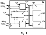
- FIG. 1 shows a schematic of the components of an integrated circuit implementing a radio frequency (RF) built-in-self-test (BIST) network according to an embodiment of this disclosure.
- the integrated circuit comprises a microcontroller unit (MCU), although this is not essential.
- MCU microcontroller unit
- the MCU may include a processor core 135 and a number of peripherals 132, 134.
- the MCU 10 includes a plurality of radio circuits 112, 114. In this embodiment only two radio circuits 112, 114 are shown, but it is envisaged that more than two radio circuits may be present, allowing for easy scalability of the device.
- Each radio circuit has a radio circuit input and a radio circuit output. In this embodiment a radio circuit output of the radio circuit 112 is coupled to an output 102A of the MCU 10 and a radio circuit input of the radio circuit 112 is coupled to an input 102B of the MCU 10, to allow the radio circuit 112 to send and receive RF signals via an RF transmitter.
- a radio circuit output of the radio circuit 114 is coupled to an output 106A of the MCU 10 and a radio circuit input of the radio circuit 114 is coupled to an input 106B of the MCU 10, to allow the radio circuit 112 to send and receive RF signals via an RF transmitter.
- the MCU 10 also includes a switching network 116 for performing a built-in-self-test (BIST) procedure. As shown in Figure 1 , the radio circuit input and the radio circuit output of each radio circuit is coupled to the switching network 116.
- the MCU 10 may also include a diagnostic interface 104 coupled to the switching network 116, for receiving and/or outputting diagnostic signals.
- each radio circuit 112, 114, the switching network 116, the processor core 136 and the peripherals 132, 134 may be communicatively coupled together via a bus 120.
- the processor core 136 may include circuitry for controlling the switching network 116 and the radio circuits 112, 114 to perform the BIST procedure, in one or more operational modes to be described in more detail below.
- FIG 2 shows another schematic of the MCU 10 of Figure 1 , in which the switching network 116 is shown in more detail.
- integrated circuit may have more than two radio circuits.
- the integrated circuit has three radio circuits, but again it is envisaged that a larger number of radio circuits may be present, allowing for easy scalability of the device.
- the radio circuits and their respective radio circuit outputs are indicated using the reference numerals 2, 4, 6.
- the radio circuits and their respective radio circuit inputs are indicated using the reference numerals 92, 94, 96.
- the switching network 116 includes a plurality of combiners 22, 24, 26.
- the number of combiners provided in the switching network 116 may be the same as the number of radio circuits.
- Each combiner 22, 24, 26 has an input and an output.
- the combiner 22 has an input 21A and an output 21B
- the combiner 24 has an input 23A and an output 23B
- the combiner 26 has an input 25A and an output 25B.
- the switching network 116 also includes a plurality of transmitter connection switches 12, 14, 16.
- the number of transmitter connection switches provided in the switching network 116 may be the same as the number of radio circuits.
- Each transmitter connection switch 12, 14, 16 has an input and an output.
- the transmitter connection switch 12 has an input 11A and an output 11B
- the transmitter connection switch 14 has an input 13A and an output 13B
- the transmitter connection switch 16 has an input 15A and an output 15B.
- the input 11A of the transmitter connection switch 12 may be coupled to the radio circuit output 2
- the input 13A of the transmitter connection switch 14 may be coupled to the radio circuit output 4
- the input 15A of the transmitter connection switch 16 may be coupled to the radio circuit output 6.
- the output 11B of the transmitter connection switch 12 may be coupled to the inputs 21A, 23A, 25A of each of the combiners 22, 24, 26.
- the output 13B of the transmitter connection switch 14 may be coupled to the inputs 21A, 23A, 25A of each of the combiners 22, 24, 26.
- the output 15B of the transmitter connection switch 16 may be coupled to the inputs 21A, 23A, 25A of each of the combiners 22, 24, 26.
- each output 11B, 13B, 15B shown in Figure 2 may in some embodiments comprise a plurality of sub-outputs and the inputs 21A, 23A, 25A may similarly comprise a plurality of sub-inputs. For clarity, these sub-outputs and sub-inputs are described herein collectively (and illustrated in Figure 2 using the dotted ellipses/circles).
- the couplings described above can allow the transmitter connection switches 12, 14, 16 selectively to couple each radio circuit output 2, 4, 6 to the input 21A, 23A, 25A of each of the combiners 22, 24, 26.
- Each combiner 22, 24, 26 may be operable to combine and output each of the signals received from the radio circuit outputs 2, 4, 6 via the transmitter connection switches 12, 14, 16.
- the switching network 116 further includes a combiner switch 32.
- the combiner switch 32 has an input 31A and an output 31B.
- the input 31A of the combiner switch 32 is coupled to the output 21B, 23B, 25B of each combiner 22, 24, 26.
- the combiner switch 32 is operable selectively to output an output signal received from each of the combiners 22, 24, 26 for routing a combined signal through the switching network 116.
- the input 31A shown in Figure 2 may in some embodiments comprise a plurality of sub-inputs (for coupling to each combiner 22, 24, 26, respectively). For clarity, these sub-inputs are described herein collectively (and illustrated in Figure 2 using the dotted ellipses/circles).
- the switching network 116 also includes a splitter switch 62.
- the splitter switch 62 has an input 61A and an output 61B.
- the input 61A is coupled to the output 31B of the combiner switch 32 via one or more further switches 42, 52.
- the switching network 116 further includes a plurality of splitters 72, 74, 76.
- Each splitter has an input 71A, 73A, 75A and an output 71B, 73B, 75B.
- the input of each splitter 72, 74, 76 is coupled to the output 61B of the splitter switch 62.
- the splitter switch 62 may be operable selectively to output an output signal received from the one or more further switches 42, 52 (e.g. a signal routed to the splitter switch 62 from the combiner switch 32 via the one or more further switches 42, 52) to one of the splitters 72, 74, 76.
- output 61B shown in Figure 2 may in some embodiments comprise a plurality of sub-outputs (for coupling to each splitter 72, 74, 76, respectively). For clarity, these sub-outputs are described herein collectively (and illustrated in Figure 2 using the dotted ellipses/circles).
- the switching network 116 also includes a plurality of receiver connection switches 82, 84, 86.
- the receiver connection switch 82 has an input 81A and an output 81B.
- the receiver connection switch 84 has an input 83A and an output 83B.
- the receiver connection switch 86 has an input 85A and an output 85B.
- the outputs 81B, 83B, 85B are coupled to the radio circuit inputs 92, 94, 96, respectively. Accordingly, each receiver connection switch 82, 84, 86 is operable selectively to couple the output of each splitter 72, 74, 76 to one of the radio circuit inputs 92, 94, 96.
- each output 71B, 73B, 75B shown in Figure 2 may in some embodiments comprise a plurality of sub-outputs (for coupling to each receiver connection switch 82, 84, 86, respectively).
- each input 81A, 83A, 85A may in some embodiments comprise a plurality of sub-inputs (for coupling to each splitter 72, 74, 76, respectively).
- these sub-outputs and sub-inputs are described herein collectively (and illustrated in Figure 2 using the dotted ellipses/circles).
- the features of the switching network 116 described above can allow the switching network 116 to operate in the parallel testing mode to be described below in relation to Figure 3 .
- the switching network 116 may further include a splitter bypass switch 64.
- the splitter bypass switch 64 can allow the splitter switch 62 and the splitters 72, 74, 76 to be bypassed in some operational modes.
- the one or more further switches 42, 52 may be operable in those operational modes to route received signals to the splitter bypass switch 64 instead of the splitter switch 62.
- the splitter bypass switch 64 has an input 63A and an output 63B.
- the input 63A is coupled to the output 31B of the combiner switch 32 via the one or more further switches 42, 52.
- the input 63A may also be coupled to the combiner bypass switch 36 (to be described below) via the one or more further switches 42, 52.
- the output 63B is coupled to the input of each receiver connection switch 82, 84, 86. This can allow each receiver connection switch 82, 84, 86 selectively to couple an output of the splitter bypass switch 64 to one of the radio circuit inputs.
- each input 81A, 83A, 85A may in some embodiments include a respective sub-input for coupling to the splitter bypass switch 64.
- these sub-outputs and sub-inputs are described herein collectively (and illustrated in Figure 2 using the dotted ellipses/circles).
- the features of the switching network 116 including the splitter bypass switch 64 described above can allow the switching network 116 to operate in the sequential testing mode mode to be described below in relation to Figure 4 .
- the switching network 116 may further include a combiner bypass switch 36.
- the combiner bypass switch 36 may allow the combiners 22, 24, 26 and the combiner switch 32 to be bypassed in some operational modes of the switching network 116. Instead, in those operational modes, the signals received from the radio circuit outputs 2, 4, 6 may be routed through the switching network 116 via the combiner bypass switch 36.
- the combiner bypass switch 36 has an input 35A and an output 35B.
- the input 35A of the combiner bypass switch 36 is coupled to the output 11B, 13B, 15B of each transmitter connection switch 12, 14, 16.
- the output 35B of the combiner bypass switch 36 is coupled to the input 61A of the splitter switch 62 and or coupled to the input 63A of the splitter bypass switch 64 via the one or more further switches 42, 52.
- each output 11B, 13B, 15B may in some embodiments include a respective sub-output for coupling to the combiner bypass switch 36.
- these sub-outputs and sub-inputs are described herein collectively (and illustrated in Figure 2 using the dotted ellipses/circles).
- the features of the switching network 116 including the combiner bypass switch 36 described above can allow the switching network 116 to operate in the parallel testing mode to be described below in relation to Figure 5 .
- the switching network 116 may further include a diagnostic output 8.
- the diagnostic output 8 may be coupled to the a diagnostic interface 104 described above in relation to Figure 1 .
- the switching network 116 may also include a diagnostic switch 18.
- the diagnostic switch 18 has an input 17A and an output 17B.
- the output 17B of the diagnostic switch 18 is coupled to the diagnostic output 8.
- the input 17A of the diagnostic switch 18 may be coupled to the output 31B of the combiner switch 32 via the one or more further switches 42, 52 to allow the diagnostic switch 18 to receive a combined signal from one or more of the combiners 22, 24, 26 and route it to the diagnostic output 8.
- the input 17A of the diagnostic switch 18 may alternatively (or additionally) be coupled to the output 35B of the combiner bypass switch 36 via the one or more further switches 42, 52 so as to allow the diagnostic switch 18 to route an uncombined signal from one or more of the radio circuit outputs 2, 4, 6 to the diagnostic output 8.
- the output 35B of the combiner bypass switch 36 may be coupled to the input 63A of the splitter bypass switch 64 via the one or more further switches 42, 52. This can allow the switching network 116 to operate in the sequential testing mode to be described below in relation to Figure 7 .
- the one or more further switches noted above may take any suitable form for providing the appropriate couplings between the various components of the switching network 116 described above, for operation of the switching network 116 in one or more operational modes to be described below.
- a first further switch 42 and a second further switch 52 are provided.
- the first further switch 42 includes an input 41A and an output 41B.
- the second further switch 52 includes an input 51A and an output 51B.
- the input 41A of the first further switch 42 may be coupled to the output 31B of the combiner switch 32.
- the input 41A of the first further switch 42 may be coupled to the output 35B of the combiner bypass switch 36.
- the output 41B of the first further switch 42 is coupled to the input 51A of the second further switch 52.
- the output 51B of the second further switch 52 may be coupled to the input 61A of the splitter switch 62.
- the output 51B of the second further switch 52 may be coupled to the input 62A of the splitter bypass switch 64.
- the output 51B of the second further switch 52 may be coupled to the input 17A of the diagnostic switch 18.
- the arrangement of couplings of the first and second switches can, as will be described below, allow appropriate routing of signals through the switching network 116 in the one or more operational modes of the switching network 116.
- an integrated circuit may be operable in a plurality of parallel and sequential testing modes and may also be operable in a diagnostic mode.
- the various switches and other components of the switching network may be controlled by the processor core 136 described above in relation to Figure 1 .
- the radio circuits of the integrated circuit may each produce a test signal, which is routed to the switching network 116 via the radio circuit outputs 2, 4, 6.
- the test signals may be routed through the various components of the switching network 116 to the radio circuit inputs 92, 94, 96.
- the test signals received at the radio circuit inputs 92, 94, 96 may then be evaluated.
- the diagnostic modes, the radio circuits of the integrated circuit may again each produce a test signal, which is routed to the switching network 116 via the radio circuit outputs 2, 4, 6.
- the test signals may then be routed through the various components of the switching network 116 to the diagnostic output 8 for evaluation by external diagnostic equipment.
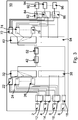
- a parallel testing mode of the switching network 116 is shown.
- the switching network 116 is operable combine, at one of the combiners 22, 24, 26, a test signal received from multiple radio circuit outputs to produce a combined signal.
- the combiner 22, 24, 26 to be used may be chosen according to factors such as the useful frequency range of each combiner 22, 24, 26 and the anticipated frequency range of the signals to be combined. By diversifying the useful frequency ranges of the combiners 22, 24, 26, increased flexibility may be provided in the BIST procedure.
- the transmitter connection switches 12, 14 16 may be controlled by the processor core 136 to route the test signals from the radio circuit outputs 2, 4, 6 to chosen combiner (in the embodiment of Figure 3 , the combiner 22 is chosen).
- the chosen combiner 22, 24, 26 may combine the signals from at least two of the radio circuit outputs 2, 4, 6 to produce the combined signal.
- the combined signal may comprise a combined signal from all of the radio circuit outputs 2, 4, 6.
- the combined signal is then routed through the combiner switch 32 (which may be controlled by the processor core 136 to select at its input 31A the output 21B of the chosen combiner 22) and the one or more further switches 42, 52 to the splitter switch 62.
- the splitter switch 62 (again under the control of the processor core 136) may then route the combined signal to one of the splitters 72, 74, 76.
- the splitter 72, 74, 76 to be used may be chosen according to factors such as the useful frequency range of each splitter 72, 74, 76 and the anticipated frequency range of the combined signal.
- the chosen splitter 72, 74, 76 would have the same useful frequency range as the chosen combiner 22, 24, 26. Again, by diversifying the useful frequency ranges of the splitters 72, 74, 76, increased flexibility may be provided in the BIST procedure.
- the chosen splitter (the splitter 72 in the example of Figure 3 ) may then route the combined signal in parallel from to each of the splitter switches 82, 84, 86.
- Each splitter switch 82, 84, 86 may then route the combined signal to a respective one of the radio circuit inputs 92, 94, 96.
- This operational mode can allow receive tests to be performed in parallel in a selected frequency band.
- the power of the test signal may be increased by combining the signals from multiple radio circuit outputs 2, 4, 6, for concurrent reception at each radio circuit input 92, 94, 96.
- the BIST procedure may, after the steps described above, switch to a next combiner/splitter pair, to perform parallel receiver testing in a different frequency band.
- the use of the combiner switch 32 and the splitter switch 62 can thus allow for convenient, fast, multi-band testing by appropriate selection of the combiner and splitter pair to be used.
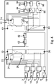
- FIG 4 a sequential testing mode of the switching network 116 is shown.
- the operation of the transmitter connection switches 12, 14, 16, the combiners 22, 24, 26 and the combiner switch 32 is similar to that described above in relation to Figure 3 .
- the one or more further switches 42, 52 route the combined signal to the splitter bypass switch 64 instead of the splitter switch 62.
- the splitters 72, 74, 76 are thereby bypassed in this mode.
- the splitter bypass switch 64 then routes the combined signal sequentially to each of the radio circuit inputs 92, 94, 96 via a respective one of the splitter switches 82, 84, 86.
- This operation mode can allow the use of combined signals in a specific frequency band (depending on the combiner chosen) to perform high power range serial receiver testing at the radio circuit inputs 92, 94, 96.
- By routing the combined signal to each radio circuit input 92, 94, 96 in a sequence (instead of concurrently) potential isolation issues between the radio circuit inputs 92, 94, 96 may be avoided.
- a parallel testing mode of the switching network 116 is shown.
- the switching network 116 (e.g. under the control of the core processor 134) routes a test signal, received at a combiner switch 12, 14, 16 from a chosen radio circuit output 2, 4, 6 (the combiner switch 12 and the radio circuit output 2 are chosen in the embodiment shown in Figure 5 ), through the combiner bypass switch 36 to the splitter switch 62 via the one or more further switches 42, 52.
- the splitter switch 62 then routes the signal to one of the splitters 72, 74, 76 (the splitter 72 is chosen in the embodiment shown in Figure 5 ).
- the chosen splitter 72 then routes the signal in parallel to each of the splitter switches 82, 84, 86.
- Each splitter switch then routes the signal to a respective one of the radio circuit inputs 92, 94, 96.
- This configuration enables the testing of several receivers (radio circuit inputs) concurrently with a test signal received from a unique radio circuit output.
- the switching network may subsequently switch to using a different radio circuit output once testing in a specific frequency band using a previous radio circuit output has been completed. In this way, more than one specific frequency band can be used in the BIST procedure.
- This operational mode can allow testing in one of more specific frequency bands.
- the splitter to be used may be chosen according to the useful frequency range of the splitter 72, 74, 76.
- the dynamic power range in this test mode may be higher than in modes using full parallel testing.
- This operational mode can allow performance of fast, higher power range testing with a unique input signal on one frequency band.
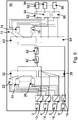
- first and second diagnostic testing modes of the switching network 116 are shown.
- the two diagnostic modes each make use of the diagnostic output 8 to allow test signals produced by the radio circuit outputs 2, 4, 6 to be evaluated by external diagnostic equipment.
- the switching network 116 (e.g. under control of the core processor 134) routes a test signal, received at a transmitter connection switch 12, 14, 16 from a radio circuit output 2, 4, 6, through the combiner bypass switch 36 to the diagnostic output 8 via the one or more further switches 42, 52 and the diagnostic switch 18.
- the switching network 116 may move on to routing a test signal received at a next transmitter connection switch 12, 14, 16 from a next radio circuit output 2, 4, 6 and so on. In this way, each radio circuit output can be evaluated/tested individually by the external diagnostic equipment.
- the switching network 116 may be operable in a second diagnostic mode to combine the test signals from multiple radio circuit outputs 2, 4, 6 into a combined signal for evaluation by the external diagnostic equipment.
- the switching network 116 may use the transmitter connection switches 12, 14, 16 to route test signals from their respective radio circuit outputs 2, 4, 6, to one of the combiners 22, 24, 26.
- the combiner 22, 24, 26 to be used may be chosen based on the useful frequency ranges of the combiners 22, 24, 26 and the anticipated frequency range of the combined test signal.
- the chosen combiner may combine the tests signals received from the multiple radio circuit outputs 2, 4, 6 to produce the combined signal, and the switching network 116 may then route the combined signal from the chosen combiner 2, 4, 6 to the diagnostic output 8 via the combiner switch 32, the one or more further switches 42, 52 and the diagnostic switch 18.
- the second diagnostic mode may further involve moving onto a next one of the combiners 22, 24, 26 after the first chosen combiner 22, 24, 26 has been used.
- the switching network 116 may sequentially combine, at at least one other of the combiners 22, 24, 26, a signal received from multiple radio circuit outputs 2, 4, 6 to produce a next combined signal, and may sequentially route each combined signal from the at least one other combiner 22, 24, 26 to the diagnostic output 8 via the combiner switch 32, the one or more further switches 42, 52 and the diagnostic switch 18.
- the first and second diagnostic modes can thus allow the integrity of the test signal to be evaluated externally by routing them back to the diagnostic output 8. This can allow extra, external measurements to be performed.
- the diagnostic modes may be used to perform regression tests or to validate the radio circuit outputs 2, 4, 6 and their test signals before using them for validation of the radio circuit inputs 92, 94, 96.
- the test signals can be evaluated individually (in a sequence) or in parallel (by combining them).
- a sequential testing mode of the switching network 116 is shown.
- the switching network 116 e.g. under the control of the core processor 134) routes a test signal received at a transmitter connection switch 12, 14, 16 from a chosen radio circuit output 2, 4, 6, to the splitter bypass switch 64 via the combiner bypass switch 36 and the one or more further switches 42, 53.
- the combiners 22, 24, 26 and the splitters 72, 74, 76 are thereby bypassed in this mode.
- the splitter bypass switch 64 then routes the test signal sequentially to each of the radio circuit inputs 92, 94, 96 via a respective one of the splitter switches 82, 84, 86.
- the radio circuit output to be used may be chosen again according to the desired power and/or frequency range.
- the radio circuit output 2 and its associated transmitter connection switch are chosen.
- the BIST procedure may move on to another radio circuit output and transmitter connection switch pair, e.g. to test at a different frequency range. In this way, each radio circuit output 92, 94 , 96 can be tested individually with each radio circuit input 2, 4, 6 in an extended sequence.
- This sequential testing operational mode is suitable for wideband transmit measurements and high input power level receive tests.
- This mode uses switches, so the losses may be relatively low and the frequency range and paths isolations may be higher compared to modes in which a splitter is used. Hence higher dynamic range measurements may be achieved.
- the test signals may thereby be used in a more efficient way by taking advantage of the factors noted above. For instance, wideband Internet of Things (IoT) tests can be handled more easily with higher power levels and a higher bandwidth. The test coverage may thereby be increased.
- IoT Internet of Things
- the integrated circuit includes a plurality of radio circuits and a switching network for performing a built-in-self-test (BIST) procedure.
- the switching network includes a plurality of combiners, a plurality of transmitter connection switches, a combiner switch, a splitter switch, a plurality of splitters and a plurality of receiver connection switches.
- the switching network may also include a splitter bypass switch and/or a combiner bypass switch.
- the components of the switching network may operate to route signals between outputs and inputs of the radio circuit to implement the built-in-self-test procedure in one or more modes involving either parallel or sequential testing of the components of the radio circuits. A diagnostic mode is also envisaged.
Landscapes
- Engineering & Computer Science (AREA)
- Physics & Mathematics (AREA)
- Computer Networks & Wireless Communication (AREA)
- Signal Processing (AREA)
- Electromagnetism (AREA)
- General Engineering & Computer Science (AREA)
- General Physics & Mathematics (AREA)
- Computer Hardware Design (AREA)
- Microelectronics & Electronic Packaging (AREA)
- Monitoring And Testing Of Transmission In General (AREA)
Abstract
Description
- The present specification relates to an integrated circuit and to a method of performing a built-in-self-test (BIST) procedure in an integrated circuit.
- In a Built-In-Self-Test (BIST) environment for multi-radio transceivers, the most common way to test various Radio Frequency (RF) receivers and transmitters is to use sequential testing. This method consists in testing one radio after the other in a serial way.
- In order to speed up the testing time, a parallel testing may be implemented. This method concurrently tests all the receivers with one or more transmitters. The formula (1) shown below may be used to calculate the time gained by using the parallel testing:

- Accordingly, in formula (1), the total test time for the parallel testing method is given by the total test time of the sequential method divided by the number of tested receivers or transmitters.
- To achieve parallel testing, some passive components such as RF combiners/splitters may be integrated. A combiner is able to sum up n signals coming from n sources. A splitter divides an input signal into several outputs, which is suitable for RF radio testing. However, these devices have several drawbacks, especially with high numbers of inputs/outputs:
- Limited bandwidth, preventing the use of out of band interferers, spurs and multiple frequency range measurements.
- High losses, making the RF signal measurement difficult, and requiring RF synthesisers to operate at their maximum limits.
- Low isolation between the channels may impact antenna input impedance and adversely affect the results.
- The use of splitters in parallel testing limits the frequency ranges of the measurements to be made.
- In addition to these limitations, some tests cannot be done in parallel with a unique radio.
- Aspects of the present disclosure are set out in the accompanying independent and dependent claims. Combinations of features from the dependent claims may be combined with features of the independent claims as appropriate and not merely as explicitly set out in the claims.
- According to an aspect of the present disclosure, there is provided an integrated circuit comprising:
- a plurality of radio circuits, wherein each radio circuit includes:
- a radio circuit input to receive signals from a respective receiver;
- a radio circuit output to output signals to a respective transmitter;
- a switching network for performing a built-in-self-test (BIST) procedure; and
- circuitry for controlling the switching network to perform the BIST procedure,
- a plurality of combiners, each combiner having an input and an output;
- a plurality of transmitter connection switches, wherein each transmitter connection switch is operable selectively to couple each radio circuit output to the input of each of the combiners;
- a combiner switch having an input and an output, wherein the input is coupled to the output of each combiner, wherein the combiner switch is operable selectively to output an output signal received from each of the combiners;
- a splitter switch having an input and an output, wherein the input of the splitter switch is coupled to an output of the combiner switch via one or more further switches;
- a plurality of splitters, each splitter having an input and an output, wherein the input of each splitter is coupled to the output of the splitter switch, wherein the splitter switch is operable selectively to output an output signal received from the one or more further switches to one of the splitters; and
- a plurality of receiver connection switches, wherein each receiver connection switch is operable selectively to couple the output of each splitter to one of the radio circuit inputs.
- An integrated circuit including the switching network may be used to perform a built-in-self-test (BIST) procedure on multiple radios.
- The switching network may including features allowing the BIST procedure to include parallel and/or sequential testing modes.
- The switching network may be operable in a parallel testing mode to:
- combine, at one of the combiners, a signal received from multiple radio circuit outputs to produce a combined signal;
- route the combined signal to the splitter switch via the one or more further switches;
- route the combined signal to one of the splitters using the splitter switch;
- route the combined signal in parallel from the splitter to each of the splitter switches; and
- route the combined signal in parallel from each splitter switch to a respective one of the radio circuit inputs.
- This parallel testing mode may allow multiple radio circuit inputs to be tested concurrently. This parallel testing mode may allow fast multi-band testing to be achieved. The combiner used in this parallel testing mode may be chosen according to a frequency range of the BIST procedure.
- The switching network may further comprise a splitter bypass switch having an input coupled to the output of the combiner switch via the one or more further switches. Each receiver connection switch may further be operable selectively to couple an output of the splitter bypass switch to one of the radio circuit inputs.
- The switching network may be operable in a sequential testing mode to:
- combine, at one of the combiners, a signal received from multiple radio circuit outputs to produce a combined signal;
- route the combined signal to the splitter bypass switch via the one or more further switches;
- route the combined signal sequentially from the splitter bypass switch to each of the radio circuit inputs via a respective one of the splitter switches.
- This sequential testing mode may allow sequential testing of each radio circuit input using a combined (and potentially therefore high power) signal. The combiner used in this sequential testing mode may be chosen according to a frequency range of the BIST procedure.
- The switching network may further comprise a combiner bypass switch having an input coupled to an output of each transmitter connection switch. An output of the combiner bypass switch may be coupled to the input of the splitter switch via the one or more further switches.
- The switching network may be operable in a parallel testing mode to:
- route a signal, received at a combiner switch from a radio circuit output, through the combiner bypass switch to the splitter switch via the one or more further switches;
- route the signal to one of the splitters using the splitter switch;
- route the signal in parallel from the splitter to each of the splitter switches; and
- route the signal in parallel from each splitter switch to a respective one of the radio circuit inputs.
- This parallel testing mode may allow multiple radio circuit inputs to be tested concurrently, using a signal received from a unique radio circuit output (e.g. in a single frequency band).
- The integrated circuit may further comprise a diagnostic output and a diagnostic switch having an input and an output. The output of the diagnostic switch may be coupled to the diagnostic output. The input of the diagnostic switch may be coupled to the output of the combiner switch via the one or more further switches. Alternatively, or in addition, the input of the diagnostic switch may be coupled to the output of the combiner bypass switch via the one or more further switches.
- The switching network may be operable in a first diagnostic mode to route a signal, received at a transmitter connection switch from a radio circuit output, through the combiner bypass switch to the diagnostic output via the one or more further switches and the diagnostic switch.
- The switching network may be operable in a second diagnostic mode to:
- combine, at one of the combiners, a signal received from multiple radio circuit outputs to produce a combined signal; and
- route the combined signal from the combiner to the diagnostic output via the combiner switch, the one or more further switches and the diagnostic switch.
- The switching network may be operable in the second diagnostic mode to:
- sequentially combine, at at least one other of the combiners, a signal received from multiple radio circuit outputs to produce a combined signal; and
- sequentially route each combined signal from the at least one other combiner to the diagnostic output via the combiner switch, the one or more further switches and the diagnostic switch.
- The first and second diagnostic modes may allow external diagnostic equipment to be coupled to the diagnostic output for assessing the signals produced by the radio circuit outputs. In the first diagnostic mode, the signals from multiple radio circuit outputs may be combined and the combined signal may be assessed by the external diagnostic equipment. In the second diagnostic mode, the signal from each radio circuit output may be assessed sequentially by the external diagnostic equipment.
- An output of the combiner bypass switch may be coupled to the input of the splitter bypass switch via the one or more further switches.
- The switching network may be operable in a sequential testing mode to:
- route a signal, received at a transmitter connection switch from a radio circuit output, to the splitter bypass switch via the combiner bypass switch and the one or more further switches; and
- route the signal sequentially from the splitter bypass switch to each of the radio circuit inputs via a respective one of the splitter switches.
- This testing mode may allow high isolation, high power, wide dynamic frequency range testing to be performed by bypassing the splitter switch and performing the test sequentially. It is envisaged that this test mode may involve sequentially routing a signal received from each radio circuit output to the splitter bypass switch, so that in radio circuit output can be used in the test procedure in sequence. In this way, the test may involving testing each radio circuit output with each radio circuit input in sequence.
- The integrated circuit may be a microcontroller.
- According to another aspect of the present disclosure, there is provided a multi-radio system comprising an integrated circuit of the kind set out above. The multi-radio system may, for instance, be a telecom system according to any of the LTE, WCDMA, GSM, GPRS, WLAN, Wifi, Bluetooth, or Zigbee standards. The multi-radio system may, for instance, be a RADAR system (e.g. for automotive applications). The multi-radio system may, for instance, be an Internet-of-Things (IoT) system.
- According to a further aspect of the present disclosure, there is provided a method of performing a built-in-self-test (BIST) procedure in an integrated circuit of the kind set out above, the method comprising:
- combining, at one of the combiners, a signal received from multiple radio circuit outputs to produce a combined signal;
- routing the combined signal to the splitter switch via the one or more further switches;
- routing the combined signal to one of the splitters using the splitter switch;
- routing the combined signal in parallel from the splitter to each of the splitter switches; and
- routing the combined signal in parallel from each splitter switch to a respective one of the radio circuit inputs.
- Embodiments of this disclosure will be described hereinafter, by way of example only, with reference to the accompanying drawings in which like reference signs relate to like elements and in which:
-
Figure 1 shows an RF BIST network implementation according to an embodiment of this disclosure; -
Figure 2 shows a switching network according to an embodiment of this disclosure; -
Figure 3 shows an example of the operation of the switching network ofFigure 2 ; -
Figure 4 shows an example of the operation of the switching network ofFigure 3 ; -
Figure 5 shows an example of the operation of the switching network ofFigure 4 ; -
Figure 6 shows an example of the operation of the switching network ofFigure 5 ; and -
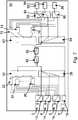
Figure 7 shows an example of the operation of the switching network ofFigure 6 . - Embodiments of this disclosure are described in the following with reference to the accompanying drawings.
-
Figure 1 shows a schematic of the components of an integrated circuit implementing a radio frequency (RF) built-in-self-test (BIST) network according to an embodiment of this disclosure. IN this embodiment, the integrated circuit comprises a microcontroller unit (MCU), although this is not essential. - The MCU may include a processor core 135 and a number of
peripherals MCU 10 includes a plurality ofradio circuits radio circuits radio circuit 112 is coupled to anoutput 102A of theMCU 10 and a radio circuit input of theradio circuit 112 is coupled to aninput 102B of theMCU 10, to allow theradio circuit 112 to send and receive RF signals via an RF transmitter. Similarly, a radio circuit output of theradio circuit 114 is coupled to anoutput 106A of theMCU 10 and a radio circuit input of theradio circuit 114 is coupled to aninput 106B of theMCU 10, to allow theradio circuit 112 to send and receive RF signals via an RF transmitter. - The
MCU 10 also includes aswitching network 116 for performing a built-in-self-test (BIST) procedure. As shown inFigure 1 , the radio circuit input and the radio circuit output of each radio circuit is coupled to theswitching network 116. TheMCU 10 may also include adiagnostic interface 104 coupled to theswitching network 116, for receiving and/or outputting diagnostic signals. - As shown in
Figure 1 , eachradio circuit switching network 116, theprocessor core 136 and theperipherals bus 120. Theprocessor core 136 may include circuitry for controlling theswitching network 116 and theradio circuits -
Figure 2 shows another schematic of theMCU 10 ofFigure 1 , in which theswitching network 116 is shown in more detail. - As noted above, integrated circuit may have more than two radio circuits. In the embodiment of
Figure 2 the integrated circuit has three radio circuits, but again it is envisaged that a larger number of radio circuits may be present, allowing for easy scalability of the device. InFigure 2 , the radio circuits and their respective radio circuit outputs are indicated using thereference numerals reference numerals - In this embodiment, the
switching network 116 includes a plurality ofcombiners switching network 116 may be the same as the number of radio circuits. Eachcombiner Figure 2 , thecombiner 22 has aninput 21A and an output 21B, thecombiner 24 has aninput 23A and anoutput 23B, and thecombiner 26 has aninput 25A and anoutput 25B. - In this embodiment, the
switching network 116 also includes a plurality of transmitter connection switches 12, 14, 16. The number of transmitter connection switches provided in theswitching network 116 may be the same as the number of radio circuits. Eachtransmitter connection switch Figure 2 , thetransmitter connection switch 12 has aninput 11A and anoutput 11B, thetransmitter connection switch 14 has aninput 13A and anoutput 13B, and thetransmitter connection switch 16 has aninput 15A and anoutput 15B. Theinput 11A of thetransmitter connection switch 12 may be coupled to theradio circuit output 2, theinput 13A of thetransmitter connection switch 14 may be coupled to theradio circuit output 4, and theinput 15A of thetransmitter connection switch 16 may be coupled to theradio circuit output 6. Theoutput 11B of thetransmitter connection switch 12 may be coupled to theinputs combiners output 13B of thetransmitter connection switch 14 may be coupled to theinputs combiners output 15B of thetransmitter connection switch 16 may be coupled to theinputs combiners output Figure 2 may in some embodiments comprise a plurality of sub-outputs and theinputs Figure 2 using the dotted ellipses/circles). - The couplings described above can allow the transmitter connection switches 12, 14, 16 selectively to couple each
radio circuit output input combiners combiner radio circuit outputs - In this embodiment, the
switching network 116 further includes acombiner switch 32. Thecombiner switch 32 has aninput 31A and anoutput 31B. Theinput 31A of thecombiner switch 32 is coupled to theoutput combiner combiner switch 32 is operable selectively to output an output signal received from each of thecombiners switching network 116. - Note that the
input 31A shown inFigure 2 may in some embodiments comprise a plurality of sub-inputs (for coupling to eachcombiner Figure 2 using the dotted ellipses/circles). - In this embodiment, the
switching network 116 also includes asplitter switch 62. Thesplitter switch 62 has aninput 61A and anoutput 61B. Theinput 61A is coupled to theoutput 31B of thecombiner switch 32 via one or morefurther switches - In this embodiment, the
switching network 116 further includes a plurality ofsplitters input output splitter output 61B of thesplitter switch 62. Thesplitter switch 62 may be operable selectively to output an output signal received from the one or morefurther switches 42, 52 (e.g. a signal routed to thesplitter switch 62 from thecombiner switch 32 via the one or morefurther switches 42, 52) to one of thesplitters - Note that the
output 61B shown inFigure 2 may in some embodiments comprise a plurality of sub-outputs (for coupling to eachsplitter Figure 2 using the dotted ellipses/circles). - In this embodiment, the
switching network 116 also includes a plurality of receiver connection switches 82, 84, 86. Thereceiver connection switch 82 has aninput 81A and anoutput 81B. Similarly, thereceiver connection switch 84 has aninput 83A and anoutput 83B. Similarly, thereceiver connection switch 86 has aninput 85A and anoutput 85B. Theoutputs radio circuit inputs receiver connection switch splitter radio circuit inputs - Note that the
outputs Figure 2 may in some embodiments comprise a plurality of sub-outputs (for coupling to eachreceiver connection switch input splitter Figure 2 using the dotted ellipses/circles). - The features of the
switching network 116 described above can allow theswitching network 116 to operate in the parallel testing mode to be described below in relation toFigure 3 . - In some embodiments, the
switching network 116 may further include asplitter bypass switch 64. Thesplitter bypass switch 64 can allow thesplitter switch 62 and thesplitters further switches splitter bypass switch 64 instead of thesplitter switch 62. - The
splitter bypass switch 64 has aninput 63A and anoutput 63B. Theinput 63A is coupled to theoutput 31B of thecombiner switch 32 via the one or morefurther switches input 63A may also be coupled to the combiner bypass switch 36 (to be described below) via the one or morefurther switches output 63B is coupled to the input of eachreceiver connection switch receiver connection switch splitter bypass switch 64 to one of the radio circuit inputs. - Note that the
output 63B shown inFigure 2 may in some embodiments comprise a plurality of sub-outputs (for coupling to eachreceiver connection switch input splitter bypass switch 64. For clarity, these sub-outputs and sub-inputs are described herein collectively (and illustrated inFigure 2 using the dotted ellipses/circles). - The features of the
switching network 116 including thesplitter bypass switch 64 described above can allow theswitching network 116 to operate in the sequential testing mode mode to be described below in relation toFigure 4 . - In some embodiments, the
switching network 116 may further include acombiner bypass switch 36. Thecombiner bypass switch 36 may allow thecombiners combiner switch 32 to be bypassed in some operational modes of theswitching network 116. Instead, in those operational modes, the signals received from theradio circuit outputs switching network 116 via thecombiner bypass switch 36. - The
combiner bypass switch 36 has an input 35A and anoutput 35B. The input 35A of thecombiner bypass switch 36 is coupled to theoutput transmitter connection switch output 35B of thecombiner bypass switch 36 is coupled to theinput 61A of thesplitter switch 62 and or coupled to theinput 63A of thesplitter bypass switch 64 via the one or morefurther switches - Note that the input 35A shown in
Figure 2 may in some embodiments comprise a plurality of sub-inputs (for coupling to eachtransmitter connection switch output combiner bypass switch 36. For clarity, these sub-outputs and sub-inputs are described herein collectively (and illustrated inFigure 2 using the dotted ellipses/circles). - The features of the
switching network 116 including thecombiner bypass switch 36 described above can allow theswitching network 116 to operate in the parallel testing mode to be described below in relation toFigure 5 . - In some embodiments, the
switching network 116 may further include adiagnostic output 8. Thediagnostic output 8 may be coupled to the adiagnostic interface 104 described above in relation toFigure 1 . In these embodiments, theswitching network 116 may also include adiagnostic switch 18. Thediagnostic switch 18 has aninput 17A and anoutput 17B. Theoutput 17B of thediagnostic switch 18 is coupled to thediagnostic output 8. Theinput 17A of thediagnostic switch 18 may be coupled to theoutput 31B of thecombiner switch 32 via the one or morefurther switches diagnostic switch 18 to receive a combined signal from one or more of thecombiners diagnostic output 8. Theinput 17A of thediagnostic switch 18 may alternatively (or additionally) be coupled to theoutput 35B of thecombiner bypass switch 36 via the one or morefurther switches diagnostic switch 18 to route an uncombined signal from one or more of theradio circuit outputs diagnostic output 8. - The features of the
switching network 116 including thecombiner bypass switch 36, thediagnostic output 8 and thediagnostic switch 18 described above can allow the switching network to operate in the first and/or second diagnostic modes to be described below in relation toFigure 6 . - As noted above, in some embodiments, the
output 35B of thecombiner bypass switch 36 may be coupled to theinput 63A of thesplitter bypass switch 64 via the one or morefurther switches switching network 116 to operate in the sequential testing mode to be described below in relation toFigure 7 . - The one or more further switches noted above may take any suitable form for providing the appropriate couplings between the various components of the
switching network 116 described above, for operation of theswitching network 116 in one or more operational modes to be described below. - In the embodiment shown in
Figure 2 , a firstfurther switch 42 and a secondfurther switch 52 are provided. The firstfurther switch 42 includes aninput 41A and anoutput 41B. The secondfurther switch 52 includes aninput 51A and anoutput 51B. Theinput 41A of the firstfurther switch 42 may be coupled to theoutput 31B of thecombiner switch 32. Theinput 41A of the firstfurther switch 42 may be coupled to theoutput 35B of thecombiner bypass switch 36. Theoutput 41B of the firstfurther switch 42 is coupled to theinput 51A of the secondfurther switch 52. Theoutput 51B of the secondfurther switch 52 may be coupled to theinput 61A of thesplitter switch 62. Theoutput 51B of the secondfurther switch 52 may be coupled to the input 62A of thesplitter bypass switch 64. Theoutput 51B of the secondfurther switch 52 may be coupled to theinput 17A of thediagnostic switch 18. - The arrangement of couplings of the first and second switches can, as will be described below, allow appropriate routing of signals through the
switching network 116 in the one or more operational modes of theswitching network 116. - A number of operational modes of the
switching network 116 will now be described with reference toFigures 3 to 7 . As will be appreciated from the description ofFigures 3 to 7 , an integrated circuit according to embodiments of this disclosure may be operable in a plurality of parallel and sequential testing modes and may also be operable in a diagnostic mode. The various switches and other components of the switching network may be controlled by theprocessor core 136 described above in relation toFigure 1 . - In each operational mode for the BIST procedure (with the exception of the diagnostic modes), the radio circuits of the integrated circuit may each produce a test signal, which is routed to the
switching network 116 via theradio circuit outputs switching network 116 to theradio circuit inputs radio circuit inputs switching network 116 via theradio circuit outputs switching network 116 to thediagnostic output 8 for evaluation by external diagnostic equipment. - In
Figure 3 , a parallel testing mode of theswitching network 116 is shown. In this mode, theswitching network 116 is operable combine, at one of thecombiners combiner combiner combiners Figure 2 , the transmitter connection switches 12, 14 16 may be controlled by theprocessor core 136 to route the test signals from theradio circuit outputs Figure 3 , thecombiner 22 is chosen). - The chosen
combiner radio circuit outputs Figure 3 , the combined signal may comprise a combined signal from all of theradio circuit outputs - As shown in
Figure 3 , the combined signal is then routed through the combiner switch 32 (which may be controlled by theprocessor core 136 to select at itsinput 31A the output 21B of the chosen combiner 22) and the one or morefurther switches splitter switch 62. The splitter switch 62 (again under the control of the processor core 136) may then route the combined signal to one of thesplitters splitter splitter splitter combiner splitters - The chosen splitter (the
splitter 72 in the example ofFigure 3 ) may then route the combined signal in parallel from to each of the splitter switches 82, 84, 86. Eachsplitter switch radio circuit inputs - This operational mode can allow receive tests to be performed in parallel in a selected frequency band. The power of the test signal may be increased by combining the signals from multiple
radio circuit outputs radio circuit input combiner switch 32 and thesplitter switch 62 can thus allow for convenient, fast, multi-band testing by appropriate selection of the combiner and splitter pair to be used. - In
Figure 4 , a sequential testing mode of theswitching network 116 is shown. In this mode, the operation of the transmitter connection switches 12, 14, 16, thecombiners combiner switch 32 is similar to that described above in relation toFigure 3 . However, in this mode, the one or morefurther switches splitter bypass switch 64 instead of thesplitter switch 62. Thesplitters - The
splitter bypass switch 64 then routes the combined signal sequentially to each of theradio circuit inputs - This operation mode can allow the use of combined signals in a specific frequency band (depending on the combiner chosen) to perform high power range serial receiver testing at the
radio circuit inputs radio circuit input radio circuit inputs - In
Figure 5 , a parallel testing mode of theswitching network 116 is shown. In this mode, the switching network 116 (e.g. under the control of the core processor 134) routes a test signal, received at acombiner switch radio circuit output combiner switch 12 and theradio circuit output 2 are chosen in the embodiment shown inFigure 5 ), through thecombiner bypass switch 36 to thesplitter switch 62 via the one or morefurther switches splitter switch 62 then routes the signal to one of thesplitters splitter 72 is chosen in the embodiment shown inFigure 5 ). The chosensplitter 72 then routes the signal in parallel to each of the splitter switches 82, 84, 86. Each splitter switch then routes the signal to a respective one of theradio circuit inputs - This configuration enables the testing of several receivers (radio circuit inputs) concurrently with a test signal received from a unique radio circuit output. As shown in
Figure 5 , the switching network may subsequently switch to using a different radio circuit output once testing in a specific frequency band using a previous radio circuit output has been completed. In this way, more than one specific frequency band can be used in the BIST procedure. - This operational mode can allow testing in one of more specific frequency bands. As described above, the splitter to be used may be chosen according to the useful frequency range of the
splitter - In
Figure 6 , first and second diagnostic testing modes of theswitching network 116 are shown. The two diagnostic modes each make use of thediagnostic output 8 to allow test signals produced by theradio circuit outputs - In the first diagnostic testing mode, the switching network 116 (e.g. under control of the core processor 134) routes a test signal, received at a
transmitter connection switch radio circuit output combiner bypass switch 36 to thediagnostic output 8 via the one or morefurther switches diagnostic switch 18. As illustrated inFigure 6 , once the test signal from one of theradio circuit outputs switching network 116 may move on to routing a test signal received at a nexttransmitter connection switch radio circuit output - In addition to, or instead of the sequential, individual evaluation of the test signals from the
radio circuit outputs radio circuit outputs switching network 116 may use the transmitter connection switches 12, 14, 16 to route test signals from their respectiveradio circuit outputs combiners combiner combiners - In the second diagnostic mode, the chosen combiner may combine the tests signals received from the multiple
radio circuit outputs switching network 116 may then route the combined signal from the chosencombiner diagnostic output 8 via thecombiner switch 32, the one or morefurther switches diagnostic switch 18. Where it is desired to externally evaluate combined test signals in a plurality of frequency bands, the second diagnostic mode may further involve moving onto a next one of thecombiners combiner switching network 116 may sequentially combine, at at least one other of thecombiners radio circuit outputs other combiner diagnostic output 8 via thecombiner switch 32, the one or morefurther switches diagnostic switch 18. - The first and second diagnostic modes can thus allow the integrity of the test signal to be evaluated externally by routing them back to the
diagnostic output 8. This can allow extra, external measurements to be performed. The diagnostic modes may be used to perform regression tests or to validate theradio circuit outputs radio circuit inputs - In
Figure 7 , a sequential testing mode of theswitching network 116 is shown. In this mode, the switching network 116 (e.g. under the control of the core processor 134) routes a test signal received at atransmitter connection switch radio circuit output splitter bypass switch 64 via thecombiner bypass switch 36 and the one or morefurther switches 42, 53. Thecombiners splitters - The
splitter bypass switch 64 then routes the test signal sequentially to each of theradio circuit inputs - The radio circuit output to be used may be chosen again according to the desired power and/or frequency range. In the embodiment shown in
Figure 7 , theradio circuit output 2 and its associated transmitter connection switch are chosen. As illustrated inFigure 2 , once the chosen radio circuit output has be used with eachradio circuit input radio circuit output radio circuit input - This sequential testing operational mode is suitable for wideband transmit measurements and high input power level receive tests. This mode uses switches, so the losses may be relatively low and the frequency range and paths isolations may be higher compared to modes in which a splitter is used. Hence higher dynamic range measurements may be achieved. The test signals may thereby be used in a more efficient way by taking advantage of the factors noted above. For instance, wideband Internet of Things (IoT) tests can be handled more easily with higher power levels and a higher bandwidth. The test coverage may thereby be increased.
- Accordingly, there has been described an integrated circuit and a method of performing a built-in-self-test (BIST) procedure in an integrated circuit. The integrated circuit includes a plurality of radio circuits and a switching network for performing a built-in-self-test (BIST) procedure. The switching network includes a plurality of combiners, a plurality of transmitter connection switches, a combiner switch, a splitter switch, a plurality of splitters and a plurality of receiver connection switches. The switching network may also include a splitter bypass switch and/or a combiner bypass switch. The components of the switching network may operate to route signals between outputs and inputs of the radio circuit to implement the built-in-self-test procedure in one or more modes involving either parallel or sequential testing of the components of the radio circuits. A diagnostic mode is also envisaged.
- Although particular embodiments of this disclosure have been described, it will be appreciated that many modifications/additions and/or substitutions may be made within the scope of the claims.
Claims (15)
- An integrated circuit comprising:a plurality of radio circuits, wherein each radio circuit includes:a radio circuit input to receive signals from a respective receiver;a radio circuit output to output signals to a respective transmitter;a switching network for performing a built-in-self-test (BIST) procedure; andcircuitry for controlling the switching network to perform said BIST procedure,wherein the switching network comprises:a plurality of combiners, each combiner having an input and an output;a plurality of transmitter connection switches, wherein each transmitter connection switch is operable selectively to couple each radio circuit output to the input of each of said combiners;a combiner switch having an input and an output, wherein the input is coupled to the output of each combiner, wherein the combiner switch is operable selectively to output an output signal received from each of said combiners;a splitter switch having an input and an output, wherein the input of the splitter switch is coupled to an output of the combiner switch via one or more further switches;a plurality of splitters, each splitter having an input and an output, wherein the input of each splitter is coupled to the output of the splitter switch, wherein the splitter switch is operable selectively to output an output signal received from the one or more further switches to one of said splitters; anda plurality of receiver connection switches, wherein each receiver connection switch is operable selectively to couple the output of each splitter to one of said radio circuit inputs.
- The integrated circuit of claim 1, wherein the switching network is operable in a parallel testing mode to:combine, at one of the combiners, a signal received from multiple radio circuit outputs to produce a combined signal;route the combined signal to the splitter switch via the one or more further switches;route the combined signal to one of the splitters using the splitter switch;route the combined signal in parallel from said splitter to each of the splitter switches; androute the combined signal in parallel from each splitter switch to a respective one of the radio circuit inputs.
- The integrated circuit of claim 1 or claim 2, wherein the switching network further comprises a splitter bypass switch having an input coupled to the output of the combiner switch via said one or more further switches, wherein each receiver connection switch is further operable selectively to couple an output of the splitter bypass switch to one of said radio circuit inputs.
- The integrated circuit of claim 3, wherein the switching network is operable in a sequential testing mode to:combine, at one of the combiners, a signal received from multiple radio circuit outputs to produce a combined signal;route the combined signal to the splitter bypass switch via the one or more further switches;route the combined signal sequentially from the splitter bypass switch to each of the radio circuit inputs via a respective one of the splitter switches.
- The integrated circuit of any preceding claim, wherein the switching network further comprises a combiner bypass switch having an input coupled to an output of each transmitter connection switch, wherein an output of the combiner bypass switch is coupled to the input of the splitter switch via said one or more further switches.
- The integrated circuit of claim 5, wherein the switching network is operable in a parallel testing mode to:route a signal, received at a combiner switch from a radio circuit output, through the combiner bypass switch to the splitter switch via the one or more further switches;route the signal to one of the splitters using the splitter switch;route the signal in parallel from said splitter to each of the splitter switches; androute the signal in parallel from each splitter switch to a respective one of the radio circuit inputs.
- The integrated circuit of claim 5 or claim 6, further comprising:a diagnostic output; anda diagnostic switch having an input and an output,wherein the output of the diagnostic switch is coupled to the diagnostic output, and wherein the input of the diagnostic switch is coupled to:the output of the combiner switch via the one or more further switches; and/orthe output of the combiner bypass switch via the one or more further switches.
- The integrated circuit of claim 7, wherein the switching network is operable in a first diagnostic mode to:
route a signal, received at a transmitter connection switch from a radio circuit output, through the combiner bypass switch to the diagnostic output via the one or more further switches and the diagnostic switch. - The integrated circuit of claim 7 or claim 8, wherein the switching network is operable in a second diagnostic mode to:combine, at one of the combiners, a signal received from multiple radio circuit outputs to produce a combined signal; androute the combined signal from the combiner to the diagnostic output via the combiner switch, the one or more further switches and the diagnostic switch.
- The integrated circuit of claim 9, wherein the switching network is operable in the second diagnostic mode to:sequentially combine, at at least one other of the combiners, a signal received from multiple radio circuit outputs to produce a combined signal; andsequentially route each combined signal from the at least one other combiner to the diagnostic output via the combiner switch, the one or more further switches and the diagnostic switch.
- The integrated circuit of any of claims 5 to 10, wherein an output of the combiner bypass switch is coupled to the input of the splitter bypass switch via said one or more further switches.
- The integrated circuit of claim 11, wherein the switching network is operable in a sequential testing mode to:route a signal, received at a transmitter connection switch from a radio circuit output, to the splitter bypass switch via the combiner bypass switch and the one or more further switches; androute the signal sequentially from the splitter bypass switch to each of the radio circuit inputs via a respective one of the splitter switches.
- The integrated circuit of any preceding claim, wherein the integrated circuit is a microcontroller.
- A multi-radio system comprising the integrated circuit of any preceding claim.
- A method of performing a built-in-self-test (BIST) procedure in an integrated circuit according to any of claims 1 to 14, the method comprising:combining, at one of the combiners, a signal received from multiple radio circuit outputs to produce a combined signal;routing the combined signal to the splitter switch via the one or more further switches;routing the combined signal to one of the splitters using the splitter switch;routing the combined signal in parallel from said splitter to each of the splitter switches; androuting the combined signal in parallel from each splitter switch to a respective one of the radio circuit inputs.
Priority Applications (2)
| Application Number | Priority Date | Filing Date | Title |
|---|---|---|---|
| EP20305491.1A EP3910351B1 (en) | 2020-05-13 | 2020-05-13 | Integrated circuit and method of performing a bist procedure |
| US17/301,723 US11463182B2 (en) | 2020-05-13 | 2021-04-13 | Integrated circuit and method of performing a BIST procedure |
Applications Claiming Priority (1)
| Application Number | Priority Date | Filing Date | Title |
|---|---|---|---|
| EP20305491.1A EP3910351B1 (en) | 2020-05-13 | 2020-05-13 | Integrated circuit and method of performing a bist procedure |
Publications (2)
| Publication Number | Publication Date |
|---|---|
| EP3910351A1 true EP3910351A1 (en) | 2021-11-17 |
| EP3910351B1 EP3910351B1 (en) | 2024-03-20 |
Family
ID=71108535
Family Applications (1)
| Application Number | Title | Priority Date | Filing Date |
|---|---|---|---|
| EP20305491.1A Active EP3910351B1 (en) | 2020-05-13 | 2020-05-13 | Integrated circuit and method of performing a bist procedure |
Country Status (2)
| Country | Link |
|---|---|
| US (1) | US11463182B2 (en) |
| EP (1) | EP3910351B1 (en) |
Citations (3)
| Publication number | Priority date | Publication date | Assignee | Title |
|---|---|---|---|---|
| US5835850A (en) * | 1996-08-12 | 1998-11-10 | At&T Corp | Self-testing transceiver |
| US20130122825A1 (en) * | 2011-06-06 | 2013-05-16 | Research In Motion Limited | Systems and methods for testing radio-based devices |
| US10284236B1 (en) * | 2018-05-03 | 2019-05-07 | Infineon Technologies Ag | Multi channel self-test for RF devices |
Family Cites Families (12)
| Publication number | Priority date | Publication date | Assignee | Title |
|---|---|---|---|---|
| US5787114A (en) | 1996-01-17 | 1998-07-28 | Lsi Logic Corporation | Loop-back test system and method |
| US6006112A (en) | 1997-11-26 | 1999-12-21 | Lucent Technologies, Inc. | Transceiver with RF loopback and downlink frequency scanning |
| FI107096B (en) * | 1999-06-03 | 2001-05-31 | Nokia Networks Oy | Testing of transmitter receivers |
| US8116208B2 (en) | 2009-10-19 | 2012-02-14 | Litepoint Corporation | System and method for testing multiple digital signal transceivers in parallel |
| US9041421B2 (en) | 2011-06-13 | 2015-05-26 | Mediatek Inc. | IC, circuitry, and RF BIST system |
| TWI447410B (en) | 2011-12-19 | 2014-08-01 | 海華科技股份有限公司 | Test system and method for testing multiple sets of radio frequency modules |
| US8913504B2 (en) | 2012-05-02 | 2014-12-16 | Litepoint Corporation | System and method for initiating testing of multiple communication devices |
| US9002290B2 (en) * | 2012-05-09 | 2015-04-07 | Litepoint Corporation | System and method for testing a radio frequency (RF) multiple-input-multiple-output (MIMO) device under test (DUT) |
| US8842549B2 (en) | 2012-12-17 | 2014-09-23 | Litepoint Corporation | System and method for parallel testing of multiple data packet signal transceivers |
| US9088521B2 (en) | 2013-02-21 | 2015-07-21 | Litepoint Corporation | System and method for testing multiple data packet signal transceivers concurrently |
| GB2512586B (en) * | 2013-04-02 | 2015-08-12 | Broadcom Corp | Switch arrangement |
| US9991973B2 (en) * | 2016-06-28 | 2018-06-05 | Psemi Corporation | Integrated circuit calibration architecture |
-
2020
- 2020-05-13 EP EP20305491.1A patent/EP3910351B1/en active Active
-
2021
- 2021-04-13 US US17/301,723 patent/US11463182B2/en active Active
Patent Citations (3)
| Publication number | Priority date | Publication date | Assignee | Title |
|---|---|---|---|---|
| US5835850A (en) * | 1996-08-12 | 1998-11-10 | At&T Corp | Self-testing transceiver |
| US20130122825A1 (en) * | 2011-06-06 | 2013-05-16 | Research In Motion Limited | Systems and methods for testing radio-based devices |
| US10284236B1 (en) * | 2018-05-03 | 2019-05-07 | Infineon Technologies Ag | Multi channel self-test for RF devices |
Non-Patent Citations (1)
| Title |
|---|
| OZGUR INAC ET AL: "A Phased Array RFIC With Built-In Self-Test Capabilities", IEEE TRANSACTIONS ON MICROWAVE THEORY AND TECHNIQUES, PLENUM, USA, vol. 60, no. 1, 1 January 2012 (2012-01-01), pages 139 - 148, XP011391050, ISSN: 0018-9480, DOI: 10.1109/TMTT.2011.2170704 * |
Also Published As
| Publication number | Publication date |
|---|---|
| US20210359773A1 (en) | 2021-11-18 |
| US11463182B2 (en) | 2022-10-04 |
| EP3910351B1 (en) | 2024-03-20 |
Similar Documents
| Publication | Publication Date | Title |
|---|---|---|
| CN109307859B (en) | A Rapid Microwave Test System for Amplitude and Phase Characteristics of TR Modules | |
| US10277492B2 (en) | Mobile terminal test device and method | |
| CN105703849B (en) | A kind of radio frequency a-b box and terminal radio frequency consistency test system | |
| WO2015041767A1 (en) | System and method for testing wide band data packet signal transceivers using narrow band testers | |
| CN106385287A (en) | Multi-channel T/R assembly testing device and method | |
| CN111565082A (en) | A radio frequency matrix and test system | |
| CN107359944B (en) | Bluetooth device RF test system | |
| US10979150B2 (en) | Method of testing RF integrated circuit | |
| CN207283563U (en) | Bluetooth equipment radio frequency test system | |
| EP3910351B1 (en) | Integrated circuit and method of performing a bist procedure | |
| CN112839346A (en) | A 5G radio frequency test interface box | |
| EP3709033A1 (en) | Performance test system for testing a complex system under test | |
| CN107566056A (en) | A kind of multichannel T/R components phase conformance testing device and method | |
| CN215529026U (en) | RF filter switching device and system | |
| CN115001526A (en) | Radio frequency system, control method for radio frequency system and electronic equipment | |
| CN111464280B (en) | Multipath signal processing system, method and device | |
| CN217935623U (en) | Radio frequency chip testing device with multiple sending and multiple receiving functions | |
| CN109302243B (en) | N-port network division same frequency interference resisting scanning method | |
| CN113726451B (en) | Radio frequency filter switching device, system and method | |
| CN115951300A (en) | Self-checking method of direction-finding system and direction-finding system | |
| CN206602526U (en) | A kind of multistation passive cross modulation test device | |
| CN102340786B (en) | A kind of for beam forming calibration and the method and apparatus of aptitude tests | |
| CN106559275A (en) | A kind of throughput testing approach and device of multiple terminals | |
| CN114070433A (en) | A system and method for testing phase-shifting conversion time of multi-channel transceiver components | |
| CN102299750A (en) | Device and method for MIMO (multiple input multiple output) test |
Legal Events
| Date | Code | Title | Description |
|---|---|---|---|
| PUAI | Public reference made under article 153(3) epc to a published international application that has entered the european phase |
Free format text: ORIGINAL CODE: 0009012 |
|
| STAA | Information on the status of an ep patent application or granted ep patent |
Free format text: STATUS: THE APPLICATION HAS BEEN PUBLISHED |
|
| AK | Designated contracting states |
Kind code of ref document: A1 Designated state(s): AL AT BE BG CH CY CZ DE DK EE ES FI FR GB GR HR HU IE IS IT LI LT LU LV MC MK MT NL NO PL PT RO RS SE SI SK SM TR |
|
| B565 | Issuance of search results under rule 164(2) epc |
Effective date: 20201027 |
|
| STAA | Information on the status of an ep patent application or granted ep patent |
Free format text: STATUS: REQUEST FOR EXAMINATION WAS MADE |
|
| 17P | Request for examination filed |
Effective date: 20220517 |
|
| RBV | Designated contracting states (corrected) |
Designated state(s): AL AT BE BG CH CY CZ DE DK EE ES FI FR GB GR HR HU IE IS IT LI LT LU LV MC MK MT NL NO PL PT RO RS SE SI SK SM TR |
|
| GRAP | Despatch of communication of intention to grant a patent |
Free format text: ORIGINAL CODE: EPIDOSNIGR1 |
|
| STAA | Information on the status of an ep patent application or granted ep patent |
Free format text: STATUS: GRANT OF PATENT IS INTENDED |
|
| INTG | Intention to grant announced |
Effective date: 20231116 |
|
| GRAS | Grant fee paid |
Free format text: ORIGINAL CODE: EPIDOSNIGR3 |
|
| GRAA | (expected) grant |
Free format text: ORIGINAL CODE: 0009210 |
|
| STAA | Information on the status of an ep patent application or granted ep patent |
Free format text: STATUS: THE PATENT HAS BEEN GRANTED |
|
| AK | Designated contracting states |
Kind code of ref document: B1 Designated state(s): AL AT BE BG CH CY CZ DE DK EE ES FI FR GB GR HR HU IE IS IT LI LT LU LV MC MK MT NL NO PL PT RO RS SE SI SK SM TR |
|
| REG | Reference to a national code |
Ref country code: GB Ref legal event code: FG4D |
|
| REG | Reference to a national code |
Ref country code: CH Ref legal event code: EP |
|
| REG | Reference to a national code |
Ref country code: IE Ref legal event code: FG4D |
|
| REG | Reference to a national code |
Ref country code: DE Ref legal event code: R096 Ref document number: 602020027469 Country of ref document: DE |
|
| PG25 | Lapsed in a contracting state [announced via postgrant information from national office to epo] |
Ref country code: LT Free format text: LAPSE BECAUSE OF FAILURE TO SUBMIT A TRANSLATION OF THE DESCRIPTION OR TO PAY THE FEE WITHIN THE PRESCRIBED TIME-LIMIT Effective date: 20240320 |
|
| REG | Reference to a national code |
Ref country code: LT Ref legal event code: MG9D |
|
| PG25 | Lapsed in a contracting state [announced via postgrant information from national office to epo] |
Ref country code: GR Free format text: LAPSE BECAUSE OF FAILURE TO SUBMIT A TRANSLATION OF THE DESCRIPTION OR TO PAY THE FEE WITHIN THE PRESCRIBED TIME-LIMIT Effective date: 20240621 |
|
| PG25 | Lapsed in a contracting state [announced via postgrant information from national office to epo] |
Ref country code: HR Free format text: LAPSE BECAUSE OF FAILURE TO SUBMIT A TRANSLATION OF THE DESCRIPTION OR TO PAY THE FEE WITHIN THE PRESCRIBED TIME-LIMIT Effective date: 20240320 Ref country code: RS Free format text: LAPSE BECAUSE OF FAILURE TO SUBMIT A TRANSLATION OF THE DESCRIPTION OR TO PAY THE FEE WITHIN THE PRESCRIBED TIME-LIMIT Effective date: 20240620 |
|
| REG | Reference to a national code |
Ref country code: NL Ref legal event code: MP Effective date: 20240320 |
|
| PG25 | Lapsed in a contracting state [announced via postgrant information from national office to epo] |
Ref country code: RS Free format text: LAPSE BECAUSE OF FAILURE TO SUBMIT A TRANSLATION OF THE DESCRIPTION OR TO PAY THE FEE WITHIN THE PRESCRIBED TIME-LIMIT Effective date: 20240620 Ref country code: NO Free format text: LAPSE BECAUSE OF FAILURE TO SUBMIT A TRANSLATION OF THE DESCRIPTION OR TO PAY THE FEE WITHIN THE PRESCRIBED TIME-LIMIT Effective date: 20240620 Ref country code: LT Free format text: LAPSE BECAUSE OF FAILURE TO SUBMIT A TRANSLATION OF THE DESCRIPTION OR TO PAY THE FEE WITHIN THE PRESCRIBED TIME-LIMIT Effective date: 20240320 Ref country code: HR Free format text: LAPSE BECAUSE OF FAILURE TO SUBMIT A TRANSLATION OF THE DESCRIPTION OR TO PAY THE FEE WITHIN THE PRESCRIBED TIME-LIMIT Effective date: 20240320 Ref country code: GR Free format text: LAPSE BECAUSE OF FAILURE TO SUBMIT A TRANSLATION OF THE DESCRIPTION OR TO PAY THE FEE WITHIN THE PRESCRIBED TIME-LIMIT Effective date: 20240621 Ref country code: FI Free format text: LAPSE BECAUSE OF FAILURE TO SUBMIT A TRANSLATION OF THE DESCRIPTION OR TO PAY THE FEE WITHIN THE PRESCRIBED TIME-LIMIT Effective date: 20240320 Ref country code: BG Free format text: LAPSE BECAUSE OF FAILURE TO SUBMIT A TRANSLATION OF THE DESCRIPTION OR TO PAY THE FEE WITHIN THE PRESCRIBED TIME-LIMIT Effective date: 20240320 |
|
| REG | Reference to a national code |
Ref country code: AT Ref legal event code: MK05 Ref document number: 1668282 Country of ref document: AT Kind code of ref document: T Effective date: 20240320 |
|
| PG25 | Lapsed in a contracting state [announced via postgrant information from national office to epo] |
Ref country code: SE Free format text: LAPSE BECAUSE OF FAILURE TO SUBMIT A TRANSLATION OF THE DESCRIPTION OR TO PAY THE FEE WITHIN THE PRESCRIBED TIME-LIMIT Effective date: 20240320 Ref country code: LV Free format text: LAPSE BECAUSE OF FAILURE TO SUBMIT A TRANSLATION OF THE DESCRIPTION OR TO PAY THE FEE WITHIN THE PRESCRIBED TIME-LIMIT Effective date: 20240320 |
|
| PG25 | Lapsed in a contracting state [announced via postgrant information from national office to epo] |
Ref country code: NL Free format text: LAPSE BECAUSE OF FAILURE TO SUBMIT A TRANSLATION OF THE DESCRIPTION OR TO PAY THE FEE WITHIN THE PRESCRIBED TIME-LIMIT Effective date: 20240320 |
|
| PG25 | Lapsed in a contracting state [announced via postgrant information from national office to epo] |
Ref country code: NL Free format text: LAPSE BECAUSE OF FAILURE TO SUBMIT A TRANSLATION OF THE DESCRIPTION OR TO PAY THE FEE WITHIN THE PRESCRIBED TIME-LIMIT Effective date: 20240320 |
|
| PG25 | Lapsed in a contracting state [announced via postgrant information from national office to epo] |
Ref country code: IS Free format text: LAPSE BECAUSE OF FAILURE TO SUBMIT A TRANSLATION OF THE DESCRIPTION OR TO PAY THE FEE WITHIN THE PRESCRIBED TIME-LIMIT Effective date: 20240720 |
|
| PG25 | Lapsed in a contracting state [announced via postgrant information from national office to epo] |
Ref country code: SM Free format text: LAPSE BECAUSE OF FAILURE TO SUBMIT A TRANSLATION OF THE DESCRIPTION OR TO PAY THE FEE WITHIN THE PRESCRIBED TIME-LIMIT Effective date: 20240320 Ref country code: PT Free format text: LAPSE BECAUSE OF FAILURE TO SUBMIT A TRANSLATION OF THE DESCRIPTION OR TO PAY THE FEE WITHIN THE PRESCRIBED TIME-LIMIT Effective date: 20240722 |
|
| PG25 | Lapsed in a contracting state [announced via postgrant information from national office to epo] |
Ref country code: ES Free format text: LAPSE BECAUSE OF FAILURE TO SUBMIT A TRANSLATION OF THE DESCRIPTION OR TO PAY THE FEE WITHIN THE PRESCRIBED TIME-LIMIT Effective date: 20240320 |
|
| PG25 | Lapsed in a contracting state [announced via postgrant information from national office to epo] |
Ref country code: EE Free format text: LAPSE BECAUSE OF FAILURE TO SUBMIT A TRANSLATION OF THE DESCRIPTION OR TO PAY THE FEE WITHIN THE PRESCRIBED TIME-LIMIT Effective date: 20240320 Ref country code: CZ Free format text: LAPSE BECAUSE OF FAILURE TO SUBMIT A TRANSLATION OF THE DESCRIPTION OR TO PAY THE FEE WITHIN THE PRESCRIBED TIME-LIMIT Effective date: 20240320 |
|
| PG25 | Lapsed in a contracting state [announced via postgrant information from national office to epo] |
Ref country code: AT Free format text: LAPSE BECAUSE OF FAILURE TO SUBMIT A TRANSLATION OF THE DESCRIPTION OR TO PAY THE FEE WITHIN THE PRESCRIBED TIME-LIMIT Effective date: 20240320 |
|
| PG25 | Lapsed in a contracting state [announced via postgrant information from national office to epo] |
Ref country code: PL Free format text: LAPSE BECAUSE OF FAILURE TO SUBMIT A TRANSLATION OF THE DESCRIPTION OR TO PAY THE FEE WITHIN THE PRESCRIBED TIME-LIMIT Effective date: 20240320 |
|
| PG25 | Lapsed in a contracting state [announced via postgrant information from national office to epo] |
Ref country code: SK Free format text: LAPSE BECAUSE OF FAILURE TO SUBMIT A TRANSLATION OF THE DESCRIPTION OR TO PAY THE FEE WITHIN THE PRESCRIBED TIME-LIMIT Effective date: 20240320 |
|
| PG25 | Lapsed in a contracting state [announced via postgrant information from national office to epo] |
Ref country code: SM Free format text: LAPSE BECAUSE OF FAILURE TO SUBMIT A TRANSLATION OF THE DESCRIPTION OR TO PAY THE FEE WITHIN THE PRESCRIBED TIME-LIMIT Effective date: 20240320 Ref country code: SK Free format text: LAPSE BECAUSE OF FAILURE TO SUBMIT A TRANSLATION OF THE DESCRIPTION OR TO PAY THE FEE WITHIN THE PRESCRIBED TIME-LIMIT Effective date: 20240320 Ref country code: RO Free format text: LAPSE BECAUSE OF FAILURE TO SUBMIT A TRANSLATION OF THE DESCRIPTION OR TO PAY THE FEE WITHIN THE PRESCRIBED TIME-LIMIT Effective date: 20240320 Ref country code: PT Free format text: LAPSE BECAUSE OF FAILURE TO SUBMIT A TRANSLATION OF THE DESCRIPTION OR TO PAY THE FEE WITHIN THE PRESCRIBED TIME-LIMIT Effective date: 20240722 Ref country code: PL Free format text: LAPSE BECAUSE OF FAILURE TO SUBMIT A TRANSLATION OF THE DESCRIPTION OR TO PAY THE FEE WITHIN THE PRESCRIBED TIME-LIMIT Effective date: 20240320 Ref country code: IS Free format text: LAPSE BECAUSE OF FAILURE TO SUBMIT A TRANSLATION OF THE DESCRIPTION OR TO PAY THE FEE WITHIN THE PRESCRIBED TIME-LIMIT Effective date: 20240720 Ref country code: ES Free format text: LAPSE BECAUSE OF FAILURE TO SUBMIT A TRANSLATION OF THE DESCRIPTION OR TO PAY THE FEE WITHIN THE PRESCRIBED TIME-LIMIT Effective date: 20240320 Ref country code: EE Free format text: LAPSE BECAUSE OF FAILURE TO SUBMIT A TRANSLATION OF THE DESCRIPTION OR TO PAY THE FEE WITHIN THE PRESCRIBED TIME-LIMIT Effective date: 20240320 Ref country code: CZ Free format text: LAPSE BECAUSE OF FAILURE TO SUBMIT A TRANSLATION OF THE DESCRIPTION OR TO PAY THE FEE WITHIN THE PRESCRIBED TIME-LIMIT Effective date: 20240320 Ref country code: AT Free format text: LAPSE BECAUSE OF FAILURE TO SUBMIT A TRANSLATION OF THE DESCRIPTION OR TO PAY THE FEE WITHIN THE PRESCRIBED TIME-LIMIT Effective date: 20240320 |
|
| PG25 | Lapsed in a contracting state [announced via postgrant information from national office to epo] |
Ref country code: IT Free format text: LAPSE BECAUSE OF FAILURE TO SUBMIT A TRANSLATION OF THE DESCRIPTION OR TO PAY THE FEE WITHIN THE PRESCRIBED TIME-LIMIT Effective date: 20240320 |
|
| REG | Reference to a national code |
Ref country code: DE Ref legal event code: R097 Ref document number: 602020027469 Country of ref document: DE |
|
| REG | Reference to a national code |
Ref country code: CH Ref legal event code: PL |
|
| PG25 | Lapsed in a contracting state [announced via postgrant information from national office to epo] |
Ref country code: IT Free format text: LAPSE BECAUSE OF FAILURE TO SUBMIT A TRANSLATION OF THE DESCRIPTION OR TO PAY THE FEE WITHIN THE PRESCRIBED TIME-LIMIT Effective date: 20240320 |
|
| PG25 | Lapsed in a contracting state [announced via postgrant information from national office to epo] |
Ref country code: MC Free format text: LAPSE BECAUSE OF FAILURE TO SUBMIT A TRANSLATION OF THE DESCRIPTION OR TO PAY THE FEE WITHIN THE PRESCRIBED TIME-LIMIT Effective date: 20240320 |
|
| PG25 | Lapsed in a contracting state [announced via postgrant information from national office to epo] |
Ref country code: DK Free format text: LAPSE BECAUSE OF FAILURE TO SUBMIT A TRANSLATION OF THE DESCRIPTION OR TO PAY THE FEE WITHIN THE PRESCRIBED TIME-LIMIT Effective date: 20240320 |
|
| PG25 | Lapsed in a contracting state [announced via postgrant information from national office to epo] |
Ref country code: LU Free format text: LAPSE BECAUSE OF NON-PAYMENT OF DUE FEES Effective date: 20240513 |
|
| PLBE | No opposition filed within time limit |
Free format text: ORIGINAL CODE: 0009261 |
|
| STAA | Information on the status of an ep patent application or granted ep patent |
Free format text: STATUS: NO OPPOSITION FILED WITHIN TIME LIMIT |
|
| PG25 | Lapsed in a contracting state [announced via postgrant information from national office to epo] |
Ref country code: MC Free format text: LAPSE BECAUSE OF FAILURE TO SUBMIT A TRANSLATION OF THE DESCRIPTION OR TO PAY THE FEE WITHIN THE PRESCRIBED TIME-LIMIT Effective date: 20240320 Ref country code: LU Free format text: LAPSE BECAUSE OF NON-PAYMENT OF DUE FEES Effective date: 20240513 Ref country code: DK Free format text: LAPSE BECAUSE OF FAILURE TO SUBMIT A TRANSLATION OF THE DESCRIPTION OR TO PAY THE FEE WITHIN THE PRESCRIBED TIME-LIMIT Effective date: 20240320 Ref country code: CH Free format text: LAPSE BECAUSE OF NON-PAYMENT OF DUE FEES Effective date: 20240531 |
|
| REG | Reference to a national code |
Ref country code: BE Ref legal event code: MM Effective date: 20240531 |
|
| 26N | No opposition filed |
Effective date: 20241223 |
|
| GBPC | Gb: european patent ceased through non-payment of renewal fee |
Effective date: 20240620 |
|
| PG25 | Lapsed in a contracting state [announced via postgrant information from national office to epo] |
Ref country code: IE Free format text: LAPSE BECAUSE OF NON-PAYMENT OF DUE FEES Effective date: 20240513 |
|
| PG25 | Lapsed in a contracting state [announced via postgrant information from national office to epo] |
Ref country code: BE Free format text: LAPSE BECAUSE OF NON-PAYMENT OF DUE FEES Effective date: 20240531 Ref country code: SI Free format text: LAPSE BECAUSE OF FAILURE TO SUBMIT A TRANSLATION OF THE DESCRIPTION OR TO PAY THE FEE WITHIN THE PRESCRIBED TIME-LIMIT Effective date: 20240320 |
|
| PG25 | Lapsed in a contracting state [announced via postgrant information from national office to epo] |
Ref country code: FR Free format text: LAPSE BECAUSE OF NON-PAYMENT OF DUE FEES Effective date: 20240520 |
|
| PG25 | Lapsed in a contracting state [announced via postgrant information from national office to epo] |
Ref country code: GB Free format text: LAPSE BECAUSE OF NON-PAYMENT OF DUE FEES Effective date: 20240620 |
|
| PGFP | Annual fee paid to national office [announced via postgrant information from national office to epo] |
Ref country code: DE Payment date: 20250423 Year of fee payment: 6 |
|
| P01 | Opt-out of the competence of the unified patent court (upc) registered |
Free format text: CASE NUMBER: APP_29898/2025 Effective date: 20250623 |
|
| PG25 | Lapsed in a contracting state [announced via postgrant information from national office to epo] |
Ref country code: CY Free format text: LAPSE BECAUSE OF FAILURE TO SUBMIT A TRANSLATION OF THE DESCRIPTION OR TO PAY THE FEE WITHIN THE PRESCRIBED TIME-LIMIT; INVALID AB INITIO Effective date: 20200513 |
|
| PG25 | Lapsed in a contracting state [announced via postgrant information from national office to epo] |
Ref country code: HU Free format text: LAPSE BECAUSE OF FAILURE TO SUBMIT A TRANSLATION OF THE DESCRIPTION OR TO PAY THE FEE WITHIN THE PRESCRIBED TIME-LIMIT; INVALID AB INITIO Effective date: 20200513 |