EP3907870A1 - Power converter with overshoot protection - Google Patents
Power converter with overshoot protection Download PDFInfo
- Publication number
- EP3907870A1 EP3907870A1 EP20172718.7A EP20172718A EP3907870A1 EP 3907870 A1 EP3907870 A1 EP 3907870A1 EP 20172718 A EP20172718 A EP 20172718A EP 3907870 A1 EP3907870 A1 EP 3907870A1
- Authority
- EP
- European Patent Office
- Prior art keywords
- converter
- resonant
- circuit
- switching
- current
- Prior art date
- Legal status (The legal status is an assumption and is not a legal conclusion. Google has not performed a legal analysis and makes no representation as to the accuracy of the status listed.)
- Granted
Links
Images


Classifications
-
- H—ELECTRICITY
- H02—GENERATION; CONVERSION OR DISTRIBUTION OF ELECTRIC POWER
- H02M—APPARATUS FOR CONVERSION BETWEEN AC AND AC, BETWEEN AC AND DC, OR BETWEEN DC AND DC, AND FOR USE WITH MAINS OR SIMILAR POWER SUPPLY SYSTEMS; CONVERSION OF DC OR AC INPUT POWER INTO SURGE OUTPUT POWER; CONTROL OR REGULATION THEREOF
- H02M1/00—Details of apparatus for conversion
- H02M1/36—Means for starting or stopping converters
-
- H—ELECTRICITY
- H02—GENERATION; CONVERSION OR DISTRIBUTION OF ELECTRIC POWER
- H02M—APPARATUS FOR CONVERSION BETWEEN AC AND AC, BETWEEN AC AND DC, OR BETWEEN DC AND DC, AND FOR USE WITH MAINS OR SIMILAR POWER SUPPLY SYSTEMS; CONVERSION OF DC OR AC INPUT POWER INTO SURGE OUTPUT POWER; CONTROL OR REGULATION THEREOF
- H02M1/00—Details of apparatus for conversion
- H02M1/32—Means for protecting converters other than automatic disconnection
-
- H—ELECTRICITY
- H02—GENERATION; CONVERSION OR DISTRIBUTION OF ELECTRIC POWER
- H02M—APPARATUS FOR CONVERSION BETWEEN AC AND AC, BETWEEN AC AND DC, OR BETWEEN DC AND DC, AND FOR USE WITH MAINS OR SIMILAR POWER SUPPLY SYSTEMS; CONVERSION OF DC OR AC INPUT POWER INTO SURGE OUTPUT POWER; CONTROL OR REGULATION THEREOF
- H02M3/00—Conversion of DC power input into DC power output
- H02M3/22—Conversion of DC power input into DC power output with intermediate conversion into AC
- H02M3/24—Conversion of DC power input into DC power output with intermediate conversion into AC by static converters
- H02M3/28—Conversion of DC power input into DC power output with intermediate conversion into AC by static converters using discharge tubes with control electrode or semiconductor devices with control electrode to produce the intermediate AC
- H02M3/325—Conversion of DC power input into DC power output with intermediate conversion into AC by static converters using discharge tubes with control electrode or semiconductor devices with control electrode to produce the intermediate AC using devices of a triode or a transistor type requiring continuous application of a control signal
- H02M3/335—Conversion of DC power input into DC power output with intermediate conversion into AC by static converters using discharge tubes with control electrode or semiconductor devices with control electrode to produce the intermediate AC using devices of a triode or a transistor type requiring continuous application of a control signal using semiconductor devices only
- H02M3/337—Conversion of DC power input into DC power output with intermediate conversion into AC by static converters using discharge tubes with control electrode or semiconductor devices with control electrode to produce the intermediate AC using devices of a triode or a transistor type requiring continuous application of a control signal using semiconductor devices only in push-pull configuration
- H02M3/3376—Conversion of DC power input into DC power output with intermediate conversion into AC by static converters using discharge tubes with control electrode or semiconductor devices with control electrode to produce the intermediate AC using devices of a triode or a transistor type requiring continuous application of a control signal using semiconductor devices only in push-pull configuration with automatic control of output voltage or current
-
- H—ELECTRICITY
- H02—GENERATION; CONVERSION OR DISTRIBUTION OF ELECTRIC POWER
- H02M—APPARATUS FOR CONVERSION BETWEEN AC AND AC, BETWEEN AC AND DC, OR BETWEEN DC AND DC, AND FOR USE WITH MAINS OR SIMILAR POWER SUPPLY SYSTEMS; CONVERSION OF DC OR AC INPUT POWER INTO SURGE OUTPUT POWER; CONTROL OR REGULATION THEREOF
- H02M1/00—Details of apparatus for conversion
- H02M1/0003—Details of control, feedback or regulation circuits
- H02M1/0009—Devices or circuits for detecting current in a converter
-
- H—ELECTRICITY
- H02—GENERATION; CONVERSION OR DISTRIBUTION OF ELECTRIC POWER
- H02M—APPARATUS FOR CONVERSION BETWEEN AC AND AC, BETWEEN AC AND DC, OR BETWEEN DC AND DC, AND FOR USE WITH MAINS OR SIMILAR POWER SUPPLY SYSTEMS; CONVERSION OF DC OR AC INPUT POWER INTO SURGE OUTPUT POWER; CONTROL OR REGULATION THEREOF
- H02M1/00—Details of apparatus for conversion
- H02M1/0048—Circuits or arrangements for reducing losses
- H02M1/0054—Transistor switching losses
- H02M1/0058—Transistor switching losses by employing soft switching techniques, i.e. commutation of transistors when applied voltage is zero or when current flow is zero
-
- H—ELECTRICITY
- H02—GENERATION; CONVERSION OR DISTRIBUTION OF ELECTRIC POWER
- H02M—APPARATUS FOR CONVERSION BETWEEN AC AND AC, BETWEEN AC AND DC, OR BETWEEN DC AND DC, AND FOR USE WITH MAINS OR SIMILAR POWER SUPPLY SYSTEMS; CONVERSION OF DC OR AC INPUT POWER INTO SURGE OUTPUT POWER; CONTROL OR REGULATION THEREOF
- H02M1/00—Details of apparatus for conversion
- H02M1/0064—Magnetic structures combining different functions, e.g. storage, filtering or transformation
-
- H—ELECTRICITY
- H02—GENERATION; CONVERSION OR DISTRIBUTION OF ELECTRIC POWER
- H02M—APPARATUS FOR CONVERSION BETWEEN AC AND AC, BETWEEN AC AND DC, OR BETWEEN DC AND DC, AND FOR USE WITH MAINS OR SIMILAR POWER SUPPLY SYSTEMS; CONVERSION OF DC OR AC INPUT POWER INTO SURGE OUTPUT POWER; CONTROL OR REGULATION THEREOF
- H02M1/00—Details of apparatus for conversion
- H02M1/32—Means for protecting converters other than automatic disconnection
- H02M1/322—Means for rapidly discharging a capacitor of the converter for protecting electrical components or for preventing electrical shock
-
- Y—GENERAL TAGGING OF NEW TECHNOLOGICAL DEVELOPMENTS; GENERAL TAGGING OF CROSS-SECTIONAL TECHNOLOGIES SPANNING OVER SEVERAL SECTIONS OF THE IPC; TECHNICAL SUBJECTS COVERED BY FORMER USPC CROSS-REFERENCE ART COLLECTIONS [XRACs] AND DIGESTS
- Y02—TECHNOLOGIES OR APPLICATIONS FOR MITIGATION OR ADAPTATION AGAINST CLIMATE CHANGE
- Y02B—CLIMATE CHANGE MITIGATION TECHNOLOGIES RELATED TO BUILDINGS, e.g. HOUSING, HOUSE APPLIANCES OR RELATED END-USER APPLICATIONS
- Y02B70/00—Technologies for an efficient end-user side electric power management and consumption
- Y02B70/10—Technologies improving the efficiency by using switched-mode power supplies [SMPS], i.e. efficient power electronics conversion e.g. power factor correction or reduction of losses in power supplies or efficient standby modes
Definitions
- the invention relates to resonant converters for supplying at its output terminals, for example a LED load.
- Resonant converters are preferably operated with a frequency different from its resonant frequency.
- a load change is performed by modulating high frequency pulses of the resonant converter with a low frequency pulse width modulation PWM signal.
- PWM signal By adjusting the duty cycle of the PWM signal, a dimming of the power transmitted by the converter, and thus the resulting current through the load can be achieved.
- the object of the invention is to provide a power converter, which allows for a very accurate output current control.
- a resonant converter for supplying a load, for example a LED load.
- the resonant converter comprises a primary converter side, comprising a converter switching circuit, a secondary converter side, and a controller.
- the controller is configured to operate the converter switching circuit using pulse width modulation, for regulating a power transfer from the primary converter side to the secondary converter side.
- the resonant converter comprises an overshoot protection circuit connected to the primary converter side and/or to the controller.
- the overshoot protection circuit is configured to, at a switch-off event, effectively stop a power transfer from the primary converter side to the secondary converter side at the end of a pulse width modulation pulse. This ensures that no current overshoot occurs, and the output current can be regulated very accurately.
- the overshoot protection circuit comprises a zero crossing detection circuit, configured to detect a zero crossing of a resonant current on the primary converter side.
- the controller is configured to, at a switch-off event, switch off of the converter switching circuit at a detected zero crossing of the resonant current on the primary converter side, after the switch-off event. This allows for a significant reduction of the current overshoot.
- the primary converter side comprises a resonant inductor.
- the zero crossing detection circuit then comprises a current measuring circuit and a current measuring coil coupled to the resonant inductor.
- the current measuring circuit is configured to determine the resonant current on the primary converter side by measuring a current through the current measuring coil.
- the zero crossing detection circuit is configured to determine a zero crossing of the resonant current on the primary converter side at a zero crossing of the current through the current measuring coil. This allows for a very simple determining of the zero crossing.
- the current measuring circuit comprises a series connection of a first resistor and a second resistor, connected between the current measuring coil and a negative supply voltage. A connection point between the first resistor and the second resistor is then connected to the controller. This allows for a very simple construction of the current measuring circuit.
- the overshoot protection circuit comprises a switching frequency doubling circuit, configured to, at a switch-off event, double an operating frequency of the converter switching circuit.
- the controller is then configured to switch off the converter switching circuit after at least one switching cycle after the switch-off event. This ensures that the converter switching circuit operates for an entire switching cycle at the doubled operating frequency, which significantly reduces the energy amount stored in the resonating elements, and thereby significantly reducing the current overshoot.
- the switching frequency doubling circuit is integrated on a single integrated circuit together with the controller. This allows an especially simple implementation.
- the overshoot protection circuit additionally comprises a discharge circuit, which is configured to, at a switch-off event, discharge a primary converter side resonator while switching off the converter switching circuit.
- a discharge circuit which is configured to, at a switch-off event, discharge a primary converter side resonator while switching off the converter switching circuit. This ensures that energy still stored within the resonator on the primary converter side is discharged instead of transferred to the secondary converter side, where it would generate a current overshoot. This significantly reduced the current overshoot as well.
- the discharge circuit comprises a series connection of a discharge resistor, configured to limit a discharge current, a discharge diode configured to prevent a reverse current flow, and a discharge switch, configured to selectively activate and deactivate the discharge.
- This series connection is then connected in parallel to a resonating element on the primary converter side. This allows for a very simply construction, and for an efficient discharge of the resonator.
- the primary converter side comprises a resonator, preferably a series connection of a first capacitance, an inductance, and a second capacitance. This allows for a very accurate current control.
- the converter switching circuit is configured to operate at a switching frequency of more than 500 KHz, preferably more than 1 MHz, most preferably more than 2 MHz.
- the switching frequency is higher than a pulse width modulation frequency. This allows for a high degree of miniaturization of the converter circuit.
- the converter switching circuit comprises switching transistors.
- These switching transistors are GaN transistors. This allows for a very high switching frequency.
- the load is a light emitting diode or a plurality of light emitting diodes. This allows for a very efficient operation.
- a method for operating a resonant converter for supplying a load comprises operating a converter switching circuit of the resonant converter using pulse width modulation, for regulating a power transfer from a primary converter side of the resonant converter to a secondary converter side of the resonant converter.
- the method moreover comprises, at a switch-off event, effectively stopping a power transfer from the primary converter side to the secondary converter side at the end of a pulse width modulation pulse. This allows for an especially accurate control of the output current.
- the method comprises detecting a zero crossing of the resonant current on the primary converter side, and, at a switch-off event, switching off a converter switching circuit and a detected zero crossing of the resonant current on the primary converter side, after the switch-off event. This allows for a significant reduction of an overshoot current.
- the method comprises, at a switch-off event, doubling an operating frequency of converter switching circuit, and switching off the converter switching circuit only after at least one switching cycle after the switch off event. This allows for a further reduction in overshoot current.
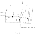
- the converter 1 comprises a primary converter side 2 and a secondary converter side 3.
- the primary converter side 2 comprises a converter switching circuit 9 comprised by two transistors HS, LS.
- the transistors HS, LS are connected in series.
- the primary converter side 2 comprises a resonator 10, comprised by first compositor CRESS, an inductance LRES, and a second capacitance CRESP, connected in this order in a series connection.
- the resonator 10 uses a LCC topology, as shown here. This results in the resonator acting as a current source, while an alternate LLC topology would result in the resonator acting as voltage source.
- the primary converter side 2 comprises a primary converter side coupling inductor 11, which is coupled to a secondary converter side coupling inductor 12, which is part of the secondary converter side 3.
- the primary converter side coupling inductor 11 and the secondary converter side coupling inductor 12 together are also referred to as coupler 4.
- the coupler 4 provides a galvanic barrier, indicated by a double dashed line.
- the converter switching circuit 9 is connected to bus voltage VBUS at a first terminal of the transistor HS.
- the resonator 10 is connected to the converter switching circuit 9 at a connection point between the transistors HS and LS.
- the second terminal of the transistor LS is connected to the second capacitor CRESP of the resonator.
- the primary converter side coupling inductor 11 is connected in parallel to the second capacitor CRESP.
- the secondary converter side coupling inductor 12 is connected to a rectifier 5, which for example is constructed from 4 diodes.
- the rectifier is connected in parallel to a capacitor 6 and a resistor 7.
- a load 8 can be connected in parallel to the rectifier 5 as well, but is not part of the converter 1.
- the converter 1 moreover comprises a controller, which is not displayed here.
- the controller is connected to the control terminals of the transistors HS, LS and therefore to the converter switching circuit 9.
- the controller controls the switching off the converter switching circuit 9, and especially the switching of the transistors HS, LS.
- the controller is adapted to control the switching circuit 9 to operate at an operating frequency, which is above the resonant frequency of the resonator 10.
- the transistors HS, LS are switched on and off repeatedly in an alternating manner at this operating frequency.
- the controller In order to regulate a power output, the controller moreover modulates the high frequency switching and the operating frequency with a pulse width modulation signal, which has a significantly lower frequency.
- the resonator 10 is supplied with energy, which is transferred to the secondary converter side by the primary converter side coupling inductor 11 and the secondary converter side coupling inductor 12.
- the energy transferred to the secondary converter side 3 is available there as an alternating current, which is rectified by the rectifier 5, and smoothed by the capacitor 6 and the resistor 7. This smoothed rectified current is provided to the load 8.
- the DC input signal on the bus is around 400 Volt.
- the DC input signal may be provided from an AC-DC-converter, e.g. a power factor correction circuit.
- a voltage of the converter switching circuit 9 is shown with reference number 20.
- a current through the load 8 is shown with reference number 21.
- a resonant current, which corresponds to a current in the resonator 10 is shown with reference number 22.
- a voltage at the transistor LS control terminal is shown with reference number 23.
- a switch-off event therein is defined as a manually or automatically transmitted signal indicating that the power to the load should be switched off.
- a first embodiment of the inventive converter 30 is shown.
- the inventive converter comprises a primary converter side 31 connected to a secondary converter side 32.
- the inventive converter 30 comprises a controller 33, which is connected to the primary converter side 31.
- the inventive converter 30 comprises an overshoot protection circuit 34, which is connected to the primary converter side 31 and to the controller 33.
- the controller 33 controls the switching of the primary converter side 31 and thereby the amount of energy transferred to the secondary converter side 32 from the primary converter side 31.
- the overshoot protection circuit 34 effectively stops power transfer from the primary converter side to the secondary converter side at the end of a pulse width modulation pulse initiated by the controller 33.
- a first option of overshoot current protection is provided in form of a second embodiment of the inventive converter.
- the circuit is identical to the circuit shown in Fig. 1 in large degrees.
- the description of the individual elements as well as their connection are omitted, as long as they are identical to the exemplary converter of Fig. 1 .
- the overshoot protection circuit 34 comprises a zero crossing detection circuit 40.
- the zero crossing detection circuit 40 comprises a current measuring coil 41, which is coupled to the first resonant inductor LRES, and a current measuring circuit 45, connected to the current measuring coil 41.
- the current measuring circuit 45 comprises, connected in series to the current measuring coil, a diode 42, a first resistance 43, and a second resistance 44. Both, the current measuring coil 41 as well as the second resistance 44 are connected at their second terminals to low supply voltage.
- a connection point between the first resistor 43 and the second resistor 44 is connected to the controller 33.
- the current through the resonant inductor LRES is mirrored as a current through the current measuring coil 41.
- This current is rectified by the diode 42 and results in a voltage between the resistors 43 and 44, which is supplied to the controller 33.
- the voltage supplied to the controller 33 correspond to the current through the current measuring coil. Therefore zero crossings of the current through the current measuring coil, as well as zero crossings of the current through the resonant inductor are provided to the controller 33.
- the controller 33 is then set up for switching off the converter switching circuit 9 only at the moment of a detected zero crossing after a switch-off event has occurred.
- the controller waits with actually switching off the converter switching circuit 9 until the next zero crossing is detected, and then switches the converter switching circuit 9 off. This significantly reduced current overshoot.
- a further method of reducing current overshoot is to increase the operating frequency, and thereby move the operating point of the resonator 10 further away from its resonance frequency, thereby reducing the amount of energy stored in the resonator 10, before switching off the converter switching circuit 9. This is for example done by a third embodiment of the inventive converter shown in Fig. 5 .
- the overshoot protection circuit 34 comprises a switching frequency doubling circuit 50.
- the operating frequency doubling circuit doubles the operating frequency at which the controller controls the operation of the converter switching circuit 9. The effect of this measure is shown and described along in Fig. 6 . It is important to note that this measure is especially effective at low operating power of the load, but is applicable at any operating power.
- switching frequency doubling circuit 50 can be implemented together with the controller 33 as part of a single integrated circuit.
- FIG. 6 the effect of using a switching frequency doubling circuit, as shown in Fig. 5 , is shown.
- reference number 60 shows the current in the resonator 10
- reference number 61 shows the voltage and the connection point between the transistors HS, LS of the converter switching circuit 9. It can readily be seen here, that for the last switching period before switching off the converter switching circuit 9, it is operated at a double frequency. This results in a significant reduction in the current overshoot.
- a further option of reducing current overshoot is to actively discharge the resonator 10 when a switch-off event occurs. This is shown in the embodiment of the inventive converter, shown in Fig. 7 . Also here, the majority of the circuit is identical to the circuit shown in Fig. 1 with regard to construction and function. Also here, only elements differing from the elements of Fig. 1 are shown.
- the overshoot protection circuit 34 here comprises a discharge circuit 70, which is connected in parallel to the second capacitor CRESP of the resonator 10.
- the discharge circuit 70 comprises a discharge resistor 71, connected to a discharge diode 72, which in turn is connected to a discharge switch 73.
- the discharge switch 73 comprises a body diode 74 which allows a certain discharge current while the discharge switch 73 is switched off. This discharge current is prevented by the discharge diode 72, which is arranged in opposite polarization.
- the discharge resistor 71 limits the amount of the discharge current.
- the discharge switch 73 is activated, at occurrence of a switch-off event. By activating the discharge switch, a discharge current, limited by the discharge resistor 72 flows through the discharge circuit, and thereby discharges energy still stored in the resonator 10. This significantly reduces the amount of current overshoot.
- the inventive converter is especially suitable for operating at high operating frequencies of the converter switching circuit 9.
- the transistors LS, HS can be switched with frequencies above 500 KHz, preferably above 1 MHz, most preferably above 2 MHz. This can especially be achieved when using GaN transistors.
- a converter switching circuit of a resonant converter is operated using pulse width modulation, for regulating a power transfer from a primary converter side to a secondary converter side.
- a second step 801 at a switch-off event, a power transfer from the primary converter side to the secondary converter side is effectively stopped at the end of a pulse width modulation pulse.
- the present invention is not limited to the embodiments and especially not to specific types of resonators or transistors.
- the present invention can be employed in a great deal of different converter types.
Landscapes
- Engineering & Computer Science (AREA)
- Power Engineering (AREA)
- Dc-Dc Converters (AREA)
Abstract
Description
- The invention relates to resonant converters for supplying at its output terminals, for example a LED load.
- Resonant converters are preferably operated with a frequency different from its resonant frequency. A load change is performed by modulating high frequency pulses of the resonant converter with a low frequency pulse width modulation PWM signal. By adjusting the duty cycle of the PWM signal, a dimming of the power transmitted by the converter, and thus the resulting current through the load can be achieved.
- When the converter is operated with a frequency different from the resonant frequency, typically higher than the resonance frequency, a switching off of the high frequency pulses of the resonant converter does not necessary lead to an immediate switching off of the power transmission between the primary converter side and the secondary converter side of the converter. Rather, it can lead to an ongoing power transmission with a relatively high peak and a resulting ripple in the output current supplied to the load. This leads to a sub-optimal switching behavior with regard to output current control.
- For example the
document EP 3 597 010 A1 shows a conventional power converter. - Accordingly, the object of the invention is to provide a power converter, which allows for a very accurate output current control.
- The object is solved by the features of the independent claims. Additional features of the invention are provided in the dependent claims. In the following, parts of the description and drawings referring to embodiments which are not covered by the claims are not presented as embodiments of the invention, but as examples useful for understanding the invention.
- According to a first aspect of the invention, a resonant converter for supplying a load, for example a LED load, is provided. The resonant converter comprises a primary converter side, comprising a converter switching circuit, a secondary converter side, and a controller. The controller is configured to operate the converter switching circuit using pulse width modulation, for regulating a power transfer from the primary converter side to the secondary converter side. The resonant converter comprises an overshoot protection circuit connected to the primary converter side and/or to the controller. The overshoot protection circuit is configured to, at a switch-off event, effectively stop a power transfer from the primary converter side to the secondary converter side at the end of a pulse width modulation pulse. This ensures that no current overshoot occurs, and the output current can be regulated very accurately.
- Preferably, the overshoot protection circuit comprises a zero crossing detection circuit, configured to detect a zero crossing of a resonant current on the primary converter side. The controller is configured to, at a switch-off event, switch off of the converter switching circuit at a detected zero crossing of the resonant current on the primary converter side, after the switch-off event. This allows for a significant reduction of the current overshoot.
- Advantageously, the primary converter side comprises a resonant inductor. The zero crossing detection circuit then comprises a current measuring circuit and a current measuring coil coupled to the resonant inductor. The current measuring circuit is configured to determine the resonant current on the primary converter side by measuring a current through the current measuring coil. The zero crossing detection circuit is configured to determine a zero crossing of the resonant current on the primary converter side at a zero crossing of the current through the current measuring coil. This allows for a very simple determining of the zero crossing.
- Advantageously, the current measuring circuit comprises a series connection of a first resistor and a second resistor, connected between the current measuring coil and a negative supply voltage. A connection point between the first resistor and the second resistor is then connected to the controller. This allows for a very simple construction of the current measuring circuit.
- Further advantageously, the overshoot protection circuit comprises a switching frequency doubling circuit, configured to, at a switch-off event, double an operating frequency of the converter switching circuit. The controller is then configured to switch off the converter switching circuit after at least one switching cycle after the switch-off event. This ensures that the converter switching circuit operates for an entire switching cycle at the doubled operating frequency, which significantly reduces the energy amount stored in the resonating elements, and thereby significantly reducing the current overshoot.
- Advantageously, the switching frequency doubling circuit is integrated on a single integrated circuit together with the controller. This allows an especially simple implementation.
- Preferably, the overshoot protection circuit additionally comprises a discharge circuit, which is configured to, at a switch-off event, discharge a primary converter side resonator while switching off the converter switching circuit. This ensures that energy still stored within the resonator on the primary converter side is discharged instead of transferred to the secondary converter side, where it would generate a current overshoot. This significantly reduced the current overshoot as well.
- Preferably, the discharge circuit comprises a series connection of a discharge resistor, configured to limit a discharge current, a discharge diode configured to prevent a reverse current flow, and a discharge switch, configured to selectively activate and deactivate the discharge. This series connection is then connected in parallel to a resonating element on the primary converter side. This allows for a very simply construction, and for an efficient discharge of the resonator.
- Further advantageously, the primary converter side comprises a resonator, preferably a series connection of a first capacitance, an inductance, and a second capacitance. This allows for a very accurate current control.
- Advantageously, the converter switching circuit is configured to operate at a switching frequency of more than 500 KHz, preferably more than 1 MHz, most preferably more than 2 MHz. The switching frequency is higher than a pulse width modulation frequency. This allows for a high degree of miniaturization of the converter circuit.
- Advantageously, the converter switching circuit comprises switching transistors. These switching transistors are GaN transistors. This allows for a very high switching frequency.
- Advantageously, the load is a light emitting diode or a plurality of light emitting diodes. This allows for a very efficient operation.
- According to a second aspect of the invention, a method for operating a resonant converter for supplying a load is provided. The method comprises operating a converter switching circuit of the resonant converter using pulse width modulation, for regulating a power transfer from a primary converter side of the resonant converter to a secondary converter side of the resonant converter. The method moreover comprises, at a switch-off event, effectively stopping a power transfer from the primary converter side to the secondary converter side at the end of a pulse width modulation pulse. This allows for an especially accurate control of the output current.
- Advantageously, the method comprises detecting a zero crossing of the resonant current on the primary converter side, and, at a switch-off event, switching off a converter switching circuit and a detected zero crossing of the resonant current on the primary converter side, after the switch-off event. This allows for a significant reduction of an overshoot current.
- Further advantageously, the method comprises, at a switch-off event, doubling an operating frequency of converter switching circuit, and switching off the converter switching circuit only after at least one switching cycle after the switch off event. This allows for a further reduction in overshoot current.
- An exemplary embodiment of the invention is no further explained with respect to the drawings, in which
- Fig. 1
- shows an exemplary converter;
- Fig. 2
- exemplary signals in an exemplary converter;
- Fig. 3
- shows a block diagram of a first embodiment of the inventive converter;
- Fig. 4
- shows a circuit diagram of a second embodiment of an inventive converter;
- Fig. 5
- shows a block diagram of a detail of a third embodiment of the inventive converter;
- Fig. 6
- shows the presentative signals in a fourth embodiment of the inventive converter;
- Fig. 7
- shows a fifth embodiment of the inventive converter in a circuit diagram, and
- Fig. 8
- shows a flow diagram of an embodiment of the inventive method.
- First, we demonstrate the function and problems of an exemplary converter along
Fig. 1 . With regard toFig. 2 - Fig. 7 , different embodiment of the inventive converter are shown and described with regard to their function. Finally, alongFig. 8 an embodiment of the inventive method is described in detail. Similar entities and reference numbers in different figures have been partially omitted. - In
Fig. 1 , anexemplary converter 1 is shown. Theconverter 1 comprises aprimary converter side 2 and asecondary converter side 3. Theprimary converter side 2 comprises aconverter switching circuit 9 comprised by two transistors HS, LS. The transistors HS, LS are connected in series. Moreover, theprimary converter side 2 comprises aresonator 10, comprised by first compositor CRESS, an inductance LRES, and a second capacitance CRESP, connected in this order in a series connection. - Advantageously, the
resonator 10 uses a LCC topology, as shown here. This results in the resonator acting as a current source, while an alternate LLC topology would result in the resonator acting as voltage source. - Furthermore, the
primary converter side 2 comprises a primary converterside coupling inductor 11, which is coupled to a secondary converterside coupling inductor 12, which is part of thesecondary converter side 3. The primary converterside coupling inductor 11 and the secondary converterside coupling inductor 12 together are also referred to ascoupler 4. Thecoupler 4 provides a galvanic barrier, indicated by a double dashed line. - The
converter switching circuit 9 is connected to bus voltage VBUS at a first terminal of the transistor HS. Theresonator 10 is connected to theconverter switching circuit 9 at a connection point between the transistors HS and LS. The second terminal of the transistor LS is connected to the second capacitor CRESP of the resonator. The primary converterside coupling inductor 11 is connected in parallel to the second capacitor CRESP. - On the
secondary converter side 3, the secondary converterside coupling inductor 12 is connected to a rectifier 5, which for example is constructed from 4 diodes. The rectifier is connected in parallel to a capacitor 6 and a resistor 7. Aload 8 can be connected in parallel to the rectifier 5 as well, but is not part of theconverter 1. - The
converter 1 moreover comprises a controller, which is not displayed here. The controller is connected to the control terminals of the transistors HS, LS and therefore to theconverter switching circuit 9. The controller controls the switching off theconverter switching circuit 9, and especially the switching of the transistors HS, LS. - Especially, the controller is adapted to control the
switching circuit 9 to operate at an operating frequency, which is above the resonant frequency of theresonator 10. - The transistors HS, LS are switched on and off repeatedly in an alternating manner at this operating frequency. In order to regulate a power output, the controller moreover modulates the high frequency switching and the operating frequency with a pulse width modulation signal, which has a significantly lower frequency.
- By the operation of the
converter switching circuit 9, theresonator 10 is supplied with energy, which is transferred to the secondary converter side by the primary converterside coupling inductor 11 and the secondary converterside coupling inductor 12. - The energy transferred to the
secondary converter side 3 is available there as an alternating current, which is rectified by the rectifier 5, and smoothed by the capacitor 6 and the resistor 7. This smoothed rectified current is provided to theload 8. - Advantageously, the DC input signal on the bus is around 400 Volt. The DC input signal may be provided from an AC-DC-converter, e.g. a power factor correction circuit.
- This allows for a wide output voltage window when using the here-employed LCC topology. For a converter to be used with LED loads, a wide output current window though is advantageous. This can be facilitated by preventing an overshoot of the output current. Such an overshoot prevention is the basis of the present invention and further described along
Fig. 2 - Fig. 8 . - In
Fig. 2 representative signals in an exemplary converter, as shown inFig. 1 , are shown. Here, a voltage of theconverter switching circuit 9 is shown withreference number 20. Moreover, a current through theload 8 is shown withreference number 21. A resonant current, which corresponds to a current in theresonator 10 is shown withreference number 22. Finally, a voltage at the transistor LS control terminal is shown withreference number 23. - It can clearly be seen that in the moment of the switch-off event that can best be seen on
curve 23, the resonant current does not stop, but initially increases before reducing in form of a ripple. This actually increases the current through the load shown ascurve 21, initially. A switch-off event therein is defined as a manually or automatically transmitted signal indicating that the power to the load should be switched off. - In
Fig. 3 a first embodiment of theinventive converter 30 is shown. The inventive converter comprises aprimary converter side 31 connected to asecondary converter side 32. Moreover, theinventive converter 30 comprises acontroller 33, which is connected to theprimary converter side 31. In addition, theinventive converter 30 comprises anovershoot protection circuit 34, which is connected to theprimary converter side 31 and to thecontroller 33. - The
controller 33 controls the switching of theprimary converter side 31 and thereby the amount of energy transferred to thesecondary converter side 32 from theprimary converter side 31. Theovershoot protection circuit 34 effectively stops power transfer from the primary converter side to the secondary converter side at the end of a pulse width modulation pulse initiated by thecontroller 33. - According to the present invention, different options, which can be used separately but also in conjunction for reducing the overshoot are provided.
- In
Fig. 4 a first option of overshoot current protection is provided in form of a second embodiment of the inventive converter. The circuit is identical to the circuit shown inFig. 1 in large degrees. The description of the individual elements as well as their connection are omitted, as long as they are identical to the exemplary converter ofFig. 1 . - Here, additionally, an
overshoot protection circuit 34 is provided. Theovershoot protection circuit 34 comprises a zerocrossing detection circuit 40. The zerocrossing detection circuit 40 comprises acurrent measuring coil 41, which is coupled to the first resonant inductor LRES, and acurrent measuring circuit 45, connected to the current measuringcoil 41. Thecurrent measuring circuit 45 comprises, connected in series to the current measuring coil, adiode 42, afirst resistance 43, and asecond resistance 44. Both, the current measuringcoil 41 as well as thesecond resistance 44 are connected at their second terminals to low supply voltage. - A connection point between the
first resistor 43 and thesecond resistor 44 is connected to thecontroller 33. - In operation, the current through the resonant inductor LRES is mirrored as a current through the current measuring
coil 41. This current is rectified by thediode 42 and results in a voltage between theresistors controller 33. The voltage supplied to thecontroller 33 correspond to the current through the current measuring coil. Therefore zero crossings of the current through the current measuring coil, as well as zero crossings of the current through the resonant inductor are provided to thecontroller 33. Thecontroller 33 is then set up for switching off theconverter switching circuit 9 only at the moment of a detected zero crossing after a switch-off event has occurred. - Therefore, when a switch-off event occurs, the controller waits with actually switching off the
converter switching circuit 9 until the next zero crossing is detected, and then switches theconverter switching circuit 9 off. This significantly reduced current overshoot. - A further method of reducing current overshoot is to increase the operating frequency, and thereby move the operating point of the
resonator 10 further away from its resonance frequency, thereby reducing the amount of energy stored in theresonator 10, before switching off theconverter switching circuit 9. This is for example done by a third embodiment of the inventive converter shown inFig. 5 . - Here, only the
overshoot protection circuit 34 and its connections are shown. Theovershoot protection circuit 34 only needs to be connected to thecontroller 33. Theovershoot protection circuit 34 comprises a switchingfrequency doubling circuit 50. At a switch-off event, the operating frequency doubling circuit doubles the operating frequency at which the controller controls the operation of theconverter switching circuit 9. The effect of this measure is shown and described along inFig. 6 . It is important to note that this measure is especially effective at low operating power of the load, but is applicable at any operating power. - It is important to note that the switching
frequency doubling circuit 50 can be implemented together with thecontroller 33 as part of a single integrated circuit. - In
Fig. 6 , the effect of using a switching frequency doubling circuit, as shown inFig. 5 , is shown. Here,reference number 60 shows the current in theresonator 10, whilereference number 61 shows the voltage and the connection point between the transistors HS, LS of theconverter switching circuit 9. It can readily be seen here, that for the last switching period before switching off theconverter switching circuit 9, it is operated at a double frequency. This results in a significant reduction in the current overshoot. - A further option of reducing current overshoot is to actively discharge the
resonator 10 when a switch-off event occurs. This is shown in the embodiment of the inventive converter, shown inFig. 7 . Also here, the majority of the circuit is identical to the circuit shown inFig. 1 with regard to construction and function. Also here, only elements differing from the elements ofFig. 1 are shown. - Here, in addition to the circuit of
Fig. 1 , anovershoot protection circuit 34 is used. Theovershoot protection circuit 34 here comprises adischarge circuit 70, which is connected in parallel to the second capacitor CRESP of theresonator 10. Thedischarge circuit 70 comprises adischarge resistor 71, connected to adischarge diode 72, which in turn is connected to adischarge switch 73. Thedischarge switch 73 comprises abody diode 74 which allows a certain discharge current while thedischarge switch 73 is switched off. This discharge current is prevented by thedischarge diode 72, which is arranged in opposite polarization. Thedischarge resistor 71 limits the amount of the discharge current. - The
discharge switch 73 is activated, at occurrence of a switch-off event. By activating the discharge switch, a discharge current, limited by thedischarge resistor 72 flows through the discharge circuit, and thereby discharges energy still stored in theresonator 10. This significantly reduces the amount of current overshoot. - The inventive converter is especially suitable for operating at high operating frequencies of the
converter switching circuit 9. Especially, the transistors LS, HS can be switched with frequencies above 500 KHz, preferably above 1 MHz, most preferably above 2 MHz. This can especially be achieved when using GaN transistors. - It is important to note that three options for prevention overshoot current shown before, can be employed each one separately, or in any advantageous combination.
- Finally, in
Fig. 8 an embodiment of the inventive method is shown in a flow diagram. In afirst step 800, a converter switching circuit of a resonant converter is operated using pulse width modulation, for regulating a power transfer from a primary converter side to a secondary converter side. In asecond step 801, at a switch-off event, a power transfer from the primary converter side to the secondary converter side is effectively stopped at the end of a pulse width modulation pulse. - It is pointed out that all features described along with the device embodiments shown in
Fig. 2 - Fig. 7 are also to be understood as disclosed in conjunction with the method embodiment shown inFig. 8 . - The present invention is not limited to the embodiments and especially not to specific types of resonators or transistors. The present invention can be employed in a great deal of different converter types.
Claims (15)
- Resonant converter (30) for supplying a load (8), for example a LED load, comprising:- a primary converter side (2), comprising a converter switching circuit (9),- a secondary converter side (3), and- a controller (33),wherein the controller (33) is configured to operate the converter switching circuit (9) using pulse width modulation, for regulating a power transfer from the primary converter side (2) to the secondary converter side (3),
characterized in that
the resonant converter (30) comprises an overshoot protection circuit (34) connected to the primary converter side (2) and/or to the controller (33), configured to, at a switch-off event, effectively stop a power transfer from the primary converter side (2) to the secondary converter side (3) at the end of a pulse width modulation pulse. - Resonant converter (30) according to claim 1,
characterized in that
the overshoot protection circuit (34) comprises a zero crossing detection circuit (40), configured to detect a zero crossing of a resonant current on the primary converter side (2), and
wherein the controller (33) is configured to, at a switch-off event, switch off the converter switching circuit (9) at a detected zero crossing of the resonant current on the primary converter side (2), after the switch-off event. - Resonant converter (30) according to claim 2,
characterized in that
the primary converter side (2) comprises a resonant inductor (LRES),
the zero crossing detection circuit (40) comprises a current measuring circuit (45) and a current measuring coil (41) coupled to the resonant inductor (LRES),
the current measuring circuit (45) is configured to determine the resonant current on the primary converter side (2) by measuring a current through the current measuring coil (41), and
the zero crossing detection circuit (40) is configured to determine a zero crossing of the resonant current on the primary converter side (2) at a zero crossing of the current through the current measuring coil (41). - Resonant converter (30) according to claim 3,
characterized in that
the current measuring circuit (45) comprises a series connection of a first resistor (43) and a second resistor (44), connected between the current measuring coil (41) and a negative supply voltage, and
wherein a connection point between the first resistor (43) and the second resistor (44) is connected to the controller (33). - Resonant converter (30) according to any of the claims 1 to 4,
characterized in that
the overshoot protection circuit (34) comprises a switching frequency doubling circuit (50), configured to, at a switch-off event, double an operating frequency of the converter switching circuit (9), and
the controller (33) is configured to switch off the converter switching circuit (9) after at least one switching cycle after the switch-off event. - Resonant converter (30) according to claim 5,
characterized in that
the switching frequency doubling (50) circuit is integrated on a single integrated circuit together with the controller (33). - Resonant converter (30) according to any of the claims 1 to 6,
characterized in that
the overshoot protection circuit (34) comprises a discharge circuit (70), configured to, at a switch-off event, discharge a primary converter side resonator (10) while switching off the converter switching circuit (9). - Resonant converter (30) according to claim 7,
characterized in that
the discharge circuit (70) comprises a series connection of- a discharge resistor (71), configured to limit a discharge current,- a discharge diode (72), configured to prevent reverse current flow, and- a discharge switch (73), configured to selectively activate and deactivate the discharge,connected in parallel to a resonating element (CRESP) on the primary converter side (2). - Resonant converter (30) according to any of the claims 1 to 8,
characterized in that
the primary converter side (2) comprises a resonator (10), preferably a series connection of a first capacitor (CRESS), an inductor (LRES), and a second capacitance (CRESP) . - Resonant converter (30) according to any of the claims 1 to 9,
characterized in that
the converter switching circuit (9) is configured to operate at a switching frequency of more than 500kHz, preferably more than 1MHz, most preferably more than 2MHz, and
the switching frequency is higher than a pulse width modulation frequency. - Resonant converter (30) according to any of the claims 1 to 10,
characterized in that
the converter switching circuit (9 comprises switching transistors (HS, LS), and
wherein the switching transistors (HS, LS) are GaN transistors. - Resonant converter (30) according to any of the claims 1 to 11,
characterized in that
the load (8) is a light emitting diode or a plurality of light emitting diodes. - Method for operating a resonant converter for supplying a load, comprising the following steps:- operating a converter switching circuit of the resonant converter using pulse width modulation, for regulating a power transfer from a primary converter side of the resonant converter to a secondary converter side of the resonant converter (800),- at a switch-off event, effectively stopping a power transfer from the primary converter side to the secondary converter side at the end of a pulse width modulation pulse (801).
- Method according to claim 13,
characterized in that
the method comprises- detecting a zero crossing of a resonant current on the primary converter side, and- at a switch-off event, switching off a converter switching circuit at a detected zero crossing of the resonant current on the primary converter side, after the switch-off event. - Method according to claim 13 or 14,
characterized in that
the method comprises- at a switch-off event, doubling an operating frequency of a converter switching circuit, and- switching off the converter switching circuit only after at least one switching cycle after the switch-off event.
Priority Applications (2)
| Application Number | Priority Date | Filing Date | Title |
|---|---|---|---|
| EP20172718.7A EP3907870B1 (en) | 2020-05-04 | 2020-05-04 | Power converter with overshoot protection |
| PCT/EP2021/060626 WO2021224021A1 (en) | 2020-05-04 | 2021-04-23 | Power converter with overshoot protection |
Applications Claiming Priority (1)
| Application Number | Priority Date | Filing Date | Title |
|---|---|---|---|
| EP20172718.7A EP3907870B1 (en) | 2020-05-04 | 2020-05-04 | Power converter with overshoot protection |
Publications (2)
| Publication Number | Publication Date |
|---|---|
| EP3907870A1 true EP3907870A1 (en) | 2021-11-10 |
| EP3907870B1 EP3907870B1 (en) | 2023-07-12 |
Family
ID=70553750
Family Applications (1)
| Application Number | Title | Priority Date | Filing Date |
|---|---|---|---|
| EP20172718.7A Active EP3907870B1 (en) | 2020-05-04 | 2020-05-04 | Power converter with overshoot protection |
Country Status (2)
| Country | Link |
|---|---|
| EP (1) | EP3907870B1 (en) |
| WO (1) | WO2021224021A1 (en) |
Cited By (1)
| Publication number | Priority date | Publication date | Assignee | Title |
|---|---|---|---|---|
| EP4462665A1 (en) | 2023-05-10 | 2024-11-13 | Tridonic GmbH & Co KG | Improved isolated, primary side switched resonant converter for supplying a led load |
Families Citing this family (1)
| Publication number | Priority date | Publication date | Assignee | Title |
|---|---|---|---|---|
| EP4518129A1 (en) * | 2023-08-30 | 2025-03-05 | NXP USA, Inc. | A half-bridge circuit |
Citations (4)
| Publication number | Priority date | Publication date | Assignee | Title |
|---|---|---|---|---|
| JP2005143255A (en) * | 2003-11-10 | 2005-06-02 | Mitsumi Electric Co Ltd | Resonant power supply device and control method thereof |
| US20050122088A1 (en) * | 2003-05-12 | 2005-06-09 | International Business Machines Corporation | Power supply apparatus and power supply control device |
| EP3597010A1 (en) | 2017-05-22 | 2020-01-22 | Tridonic GmbH & Co KG | Emergency lighting converter |
| CN110932552A (en) * | 2018-09-20 | 2020-03-27 | 株洲中车时代电气股份有限公司 | Delay protection method of LLC resonant circuit |
-
2020
- 2020-05-04 EP EP20172718.7A patent/EP3907870B1/en active Active
-
2021
- 2021-04-23 WO PCT/EP2021/060626 patent/WO2021224021A1/en not_active Ceased
Patent Citations (4)
| Publication number | Priority date | Publication date | Assignee | Title |
|---|---|---|---|---|
| US20050122088A1 (en) * | 2003-05-12 | 2005-06-09 | International Business Machines Corporation | Power supply apparatus and power supply control device |
| JP2005143255A (en) * | 2003-11-10 | 2005-06-02 | Mitsumi Electric Co Ltd | Resonant power supply device and control method thereof |
| EP3597010A1 (en) | 2017-05-22 | 2020-01-22 | Tridonic GmbH & Co KG | Emergency lighting converter |
| CN110932552A (en) * | 2018-09-20 | 2020-03-27 | 株洲中车时代电气股份有限公司 | Delay protection method of LLC resonant circuit |
Cited By (2)
| Publication number | Priority date | Publication date | Assignee | Title |
|---|---|---|---|---|
| EP4462665A1 (en) | 2023-05-10 | 2024-11-13 | Tridonic GmbH & Co KG | Improved isolated, primary side switched resonant converter for supplying a led load |
| WO2024231048A1 (en) * | 2023-05-10 | 2024-11-14 | Tridonic Gmbh & Co Kg | Improved isolated, primary side switched resonant converter for supplying a led load |
Also Published As
| Publication number | Publication date |
|---|---|
| WO2021224021A1 (en) | 2021-11-11 |
| EP3907870B1 (en) | 2023-07-12 |
Similar Documents
| Publication | Publication Date | Title |
|---|---|---|
| US9473032B2 (en) | Power converter system with synchronous rectifier output stage and reduced no-load power consumption | |
| US8665613B2 (en) | Switched mode power converter and method of operation thereof | |
| US6483722B2 (en) | DC/DC converter and control method thereof | |
| JP2008206271A (en) | Integrated circuit for switching power supply control and switching power supply device | |
| KR20080079775A (en) | LED backlight driving circuit | |
| US7813151B2 (en) | Variable-mode converter control circuit and half-bridge converter having the same | |
| EP3907870B1 (en) | Power converter with overshoot protection | |
| KR20210153541A (en) | High performance two stage power converter with enhanced light load management | |
| WO2005109617A1 (en) | Power factor improving circuit and switching power supply | |
| KR100747424B1 (en) | Converter with resonant circuit elements | |
| US7440295B2 (en) | Switching mode power supply with active load detection function, and switching method thereof | |
| US11217988B2 (en) | Overvoltage source determination circuit | |
| JP5424804B2 (en) | Interleave type switching power supply | |
| CN112448586A (en) | LLC resonant power converter and method and controller for controlling the same | |
| US9742292B2 (en) | Multifunction power conversion device | |
| CN116529998A (en) | Phase Shifted Full Bridge Converter | |
| CN106464243B (en) | electronic switch | |
| US20040174721A1 (en) | Switching power supply unit | |
| US20060208969A1 (en) | Control circuit for the switch in a switching power supply | |
| EP4462665B1 (en) | Isolated, primary side switched resonant conversion for supplying a led load | |
| EP1313203A2 (en) | Half-bridge converters | |
| JP5495679B2 (en) | Power circuit | |
| US11784558B2 (en) | LLC stage for LED drivers | |
| JP4061079B2 (en) | Discharge lamp lighting device | |
| US20090296426A1 (en) | Switch mode power supply |
Legal Events
| Date | Code | Title | Description |
|---|---|---|---|
| PUAI | Public reference made under article 153(3) epc to a published international application that has entered the european phase |
Free format text: ORIGINAL CODE: 0009012 |
|
| STAA | Information on the status of an ep patent application or granted ep patent |
Free format text: STATUS: THE APPLICATION HAS BEEN PUBLISHED |
|
| AK | Designated contracting states |
Kind code of ref document: A1 Designated state(s): AL AT BE BG CH CY CZ DE DK EE ES FI FR GB GR HR HU IE IS IT LI LT LU LV MC MK MT NL NO PL PT RO RS SE SI SK SM TR |
|
| B565 | Issuance of search results under rule 164(2) epc |
Effective date: 20201006 |
|
| STAA | Information on the status of an ep patent application or granted ep patent |
Free format text: STATUS: REQUEST FOR EXAMINATION WAS MADE |
|
| 17P | Request for examination filed |
Effective date: 20220310 |
|
| RBV | Designated contracting states (corrected) |
Designated state(s): AL AT BE BG CH CY CZ DE DK EE ES FI FR GB GR HR HU IE IS IT LI LT LU LV MC MK MT NL NO PL PT RO RS SE SI SK SM TR |
|
| GRAP | Despatch of communication of intention to grant a patent |
Free format text: ORIGINAL CODE: EPIDOSNIGR1 |
|
| STAA | Information on the status of an ep patent application or granted ep patent |
Free format text: STATUS: GRANT OF PATENT IS INTENDED |
|
| INTG | Intention to grant announced |
Effective date: 20230303 |
|
| GRAS | Grant fee paid |
Free format text: ORIGINAL CODE: EPIDOSNIGR3 |
|
| GRAA | (expected) grant |
Free format text: ORIGINAL CODE: 0009210 |
|
| STAA | Information on the status of an ep patent application or granted ep patent |
Free format text: STATUS: THE PATENT HAS BEEN GRANTED |
|
| AK | Designated contracting states |
Kind code of ref document: B1 Designated state(s): AL AT BE BG CH CY CZ DE DK EE ES FI FR GB GR HR HU IE IS IT LI LT LU LV MC MK MT NL NO PL PT RO RS SE SI SK SM TR |
|
| REG | Reference to a national code |
Ref country code: CH Ref legal event code: EP |
|
| REG | Reference to a national code |
Ref country code: DE Ref legal event code: R084 Ref document number: 602020013519 Country of ref document: DE |
|
| REG | Reference to a national code |
Ref country code: IE Ref legal event code: FG4D |
|
| REG | Reference to a national code |
Ref country code: DE Ref legal event code: R096 Ref document number: 602020013519 Country of ref document: DE |
|
| REG | Reference to a national code |
Ref country code: LT Ref legal event code: MG9D |
|
| REG | Reference to a national code |
Ref country code: NL Ref legal event code: MP Effective date: 20230712 |
|
| REG | Reference to a national code |
Ref country code: AT Ref legal event code: MK05 Ref document number: 1588158 Country of ref document: AT Kind code of ref document: T Effective date: 20230712 |
|
| PG25 | Lapsed in a contracting state [announced via postgrant information from national office to epo] |
Ref country code: NL Free format text: LAPSE BECAUSE OF FAILURE TO SUBMIT A TRANSLATION OF THE DESCRIPTION OR TO PAY THE FEE WITHIN THE PRESCRIBED TIME-LIMIT Effective date: 20230712 |
|
| P01 | Opt-out of the competence of the unified patent court (upc) registered |
Effective date: 20231130 |
|
| PG25 | Lapsed in a contracting state [announced via postgrant information from national office to epo] |
Ref country code: GR Free format text: LAPSE BECAUSE OF FAILURE TO SUBMIT A TRANSLATION OF THE DESCRIPTION OR TO PAY THE FEE WITHIN THE PRESCRIBED TIME-LIMIT Effective date: 20231013 |
|
| PG25 | Lapsed in a contracting state [announced via postgrant information from national office to epo] |
Ref country code: ES Free format text: LAPSE BECAUSE OF FAILURE TO SUBMIT A TRANSLATION OF THE DESCRIPTION OR TO PAY THE FEE WITHIN THE PRESCRIBED TIME-LIMIT Effective date: 20230712 |
|
| PG25 | Lapsed in a contracting state [announced via postgrant information from national office to epo] |
Ref country code: IS Free format text: LAPSE BECAUSE OF FAILURE TO SUBMIT A TRANSLATION OF THE DESCRIPTION OR TO PAY THE FEE WITHIN THE PRESCRIBED TIME-LIMIT Effective date: 20231112 |
|
| PG25 | Lapsed in a contracting state [announced via postgrant information from national office to epo] |
Ref country code: SE Free format text: LAPSE BECAUSE OF FAILURE TO SUBMIT A TRANSLATION OF THE DESCRIPTION OR TO PAY THE FEE WITHIN THE PRESCRIBED TIME-LIMIT Effective date: 20230712 Ref country code: RS Free format text: LAPSE BECAUSE OF FAILURE TO SUBMIT A TRANSLATION OF THE DESCRIPTION OR TO PAY THE FEE WITHIN THE PRESCRIBED TIME-LIMIT Effective date: 20230712 Ref country code: PT Free format text: LAPSE BECAUSE OF FAILURE TO SUBMIT A TRANSLATION OF THE DESCRIPTION OR TO PAY THE FEE WITHIN THE PRESCRIBED TIME-LIMIT Effective date: 20231113 Ref country code: NO Free format text: LAPSE BECAUSE OF FAILURE TO SUBMIT A TRANSLATION OF THE DESCRIPTION OR TO PAY THE FEE WITHIN THE PRESCRIBED TIME-LIMIT Effective date: 20231012 Ref country code: LV Free format text: LAPSE BECAUSE OF FAILURE TO SUBMIT A TRANSLATION OF THE DESCRIPTION OR TO PAY THE FEE WITHIN THE PRESCRIBED TIME-LIMIT Effective date: 20230712 Ref country code: LT Free format text: LAPSE BECAUSE OF FAILURE TO SUBMIT A TRANSLATION OF THE DESCRIPTION OR TO PAY THE FEE WITHIN THE PRESCRIBED TIME-LIMIT Effective date: 20230712 Ref country code: IS Free format text: LAPSE BECAUSE OF FAILURE TO SUBMIT A TRANSLATION OF THE DESCRIPTION OR TO PAY THE FEE WITHIN THE PRESCRIBED TIME-LIMIT Effective date: 20231112 Ref country code: HR Free format text: LAPSE BECAUSE OF FAILURE TO SUBMIT A TRANSLATION OF THE DESCRIPTION OR TO PAY THE FEE WITHIN THE PRESCRIBED TIME-LIMIT Effective date: 20230712 Ref country code: GR Free format text: LAPSE BECAUSE OF FAILURE TO SUBMIT A TRANSLATION OF THE DESCRIPTION OR TO PAY THE FEE WITHIN THE PRESCRIBED TIME-LIMIT Effective date: 20231013 Ref country code: FI Free format text: LAPSE BECAUSE OF FAILURE TO SUBMIT A TRANSLATION OF THE DESCRIPTION OR TO PAY THE FEE WITHIN THE PRESCRIBED TIME-LIMIT Effective date: 20230712 Ref country code: ES Free format text: LAPSE BECAUSE OF FAILURE TO SUBMIT A TRANSLATION OF THE DESCRIPTION OR TO PAY THE FEE WITHIN THE PRESCRIBED TIME-LIMIT Effective date: 20230712 Ref country code: AT Free format text: LAPSE BECAUSE OF FAILURE TO SUBMIT A TRANSLATION OF THE DESCRIPTION OR TO PAY THE FEE WITHIN THE PRESCRIBED TIME-LIMIT Effective date: 20230712 |
|
| PG25 | Lapsed in a contracting state [announced via postgrant information from national office to epo] |
Ref country code: PL Free format text: LAPSE BECAUSE OF FAILURE TO SUBMIT A TRANSLATION OF THE DESCRIPTION OR TO PAY THE FEE WITHIN THE PRESCRIBED TIME-LIMIT Effective date: 20230712 |
|
| REG | Reference to a national code |
Ref country code: DE Ref legal event code: R097 Ref document number: 602020013519 Country of ref document: DE |
|
| PG25 | Lapsed in a contracting state [announced via postgrant information from national office to epo] |
Ref country code: SM Free format text: LAPSE BECAUSE OF FAILURE TO SUBMIT A TRANSLATION OF THE DESCRIPTION OR TO PAY THE FEE WITHIN THE PRESCRIBED TIME-LIMIT Effective date: 20230712 Ref country code: RO Free format text: LAPSE BECAUSE OF FAILURE TO SUBMIT A TRANSLATION OF THE DESCRIPTION OR TO PAY THE FEE WITHIN THE PRESCRIBED TIME-LIMIT Effective date: 20230712 Ref country code: EE Free format text: LAPSE BECAUSE OF FAILURE TO SUBMIT A TRANSLATION OF THE DESCRIPTION OR TO PAY THE FEE WITHIN THE PRESCRIBED TIME-LIMIT Effective date: 20230712 Ref country code: DK Free format text: LAPSE BECAUSE OF FAILURE TO SUBMIT A TRANSLATION OF THE DESCRIPTION OR TO PAY THE FEE WITHIN THE PRESCRIBED TIME-LIMIT Effective date: 20230712 Ref country code: CZ Free format text: LAPSE BECAUSE OF FAILURE TO SUBMIT A TRANSLATION OF THE DESCRIPTION OR TO PAY THE FEE WITHIN THE PRESCRIBED TIME-LIMIT Effective date: 20230712 Ref country code: SK Free format text: LAPSE BECAUSE OF FAILURE TO SUBMIT A TRANSLATION OF THE DESCRIPTION OR TO PAY THE FEE WITHIN THE PRESCRIBED TIME-LIMIT Effective date: 20230712 |
|
| PLBE | No opposition filed within time limit |
Free format text: ORIGINAL CODE: 0009261 |
|
| STAA | Information on the status of an ep patent application or granted ep patent |
Free format text: STATUS: NO OPPOSITION FILED WITHIN TIME LIMIT |
|
| PG25 | Lapsed in a contracting state [announced via postgrant information from national office to epo] |
Ref country code: IT Free format text: LAPSE BECAUSE OF FAILURE TO SUBMIT A TRANSLATION OF THE DESCRIPTION OR TO PAY THE FEE WITHIN THE PRESCRIBED TIME-LIMIT Effective date: 20230712 |
|
| 26N | No opposition filed |
Effective date: 20240415 |
|
| PG25 | Lapsed in a contracting state [announced via postgrant information from national office to epo] |
Ref country code: SI Free format text: LAPSE BECAUSE OF FAILURE TO SUBMIT A TRANSLATION OF THE DESCRIPTION OR TO PAY THE FEE WITHIN THE PRESCRIBED TIME-LIMIT Effective date: 20230712 |
|
| PG25 | Lapsed in a contracting state [announced via postgrant information from national office to epo] |
Ref country code: BG Free format text: LAPSE BECAUSE OF FAILURE TO SUBMIT A TRANSLATION OF THE DESCRIPTION OR TO PAY THE FEE WITHIN THE PRESCRIBED TIME-LIMIT Effective date: 20230712 |
|
| PG25 | Lapsed in a contracting state [announced via postgrant information from national office to epo] |
Ref country code: BG Free format text: LAPSE BECAUSE OF FAILURE TO SUBMIT A TRANSLATION OF THE DESCRIPTION OR TO PAY THE FEE WITHIN THE PRESCRIBED TIME-LIMIT Effective date: 20230712 |
|
| REG | Reference to a national code |
Ref country code: CH Ref legal event code: PL |
|
| PG25 | Lapsed in a contracting state [announced via postgrant information from national office to epo] |
Ref country code: MC Free format text: LAPSE BECAUSE OF FAILURE TO SUBMIT A TRANSLATION OF THE DESCRIPTION OR TO PAY THE FEE WITHIN THE PRESCRIBED TIME-LIMIT Effective date: 20230712 |
|
| PG25 | Lapsed in a contracting state [announced via postgrant information from national office to epo] |
Ref country code: LU Free format text: LAPSE BECAUSE OF NON-PAYMENT OF DUE FEES Effective date: 20240504 |
|
| PG25 | Lapsed in a contracting state [announced via postgrant information from national office to epo] |
Ref country code: MC Free format text: LAPSE BECAUSE OF FAILURE TO SUBMIT A TRANSLATION OF THE DESCRIPTION OR TO PAY THE FEE WITHIN THE PRESCRIBED TIME-LIMIT Effective date: 20230712 Ref country code: LU Free format text: LAPSE BECAUSE OF NON-PAYMENT OF DUE FEES Effective date: 20240504 Ref country code: CH Free format text: LAPSE BECAUSE OF NON-PAYMENT OF DUE FEES Effective date: 20240531 |
|
| REG | Reference to a national code |
Ref country code: BE Ref legal event code: MM Effective date: 20240531 |
|
| PG25 | Lapsed in a contracting state [announced via postgrant information from national office to epo] |
Ref country code: IE Free format text: LAPSE BECAUSE OF NON-PAYMENT OF DUE FEES Effective date: 20240504 |
|
| PG25 | Lapsed in a contracting state [announced via postgrant information from national office to epo] |
Ref country code: BE Free format text: LAPSE BECAUSE OF NON-PAYMENT OF DUE FEES Effective date: 20240531 |
|
| PGFP | Annual fee paid to national office [announced via postgrant information from national office to epo] |
Ref country code: DE Payment date: 20250528 Year of fee payment: 6 |
|
| PGFP | Annual fee paid to national office [announced via postgrant information from national office to epo] |
Ref country code: FR Payment date: 20250526 Year of fee payment: 6 |
|
| PG25 | Lapsed in a contracting state [announced via postgrant information from national office to epo] |
Ref country code: CY Free format text: LAPSE BECAUSE OF FAILURE TO SUBMIT A TRANSLATION OF THE DESCRIPTION OR TO PAY THE FEE WITHIN THE PRESCRIBED TIME-LIMIT; INVALID AB INITIO Effective date: 20200504 |
|
| PG25 | Lapsed in a contracting state [announced via postgrant information from national office to epo] |
Ref country code: HU Free format text: LAPSE BECAUSE OF FAILURE TO SUBMIT A TRANSLATION OF THE DESCRIPTION OR TO PAY THE FEE WITHIN THE PRESCRIBED TIME-LIMIT; INVALID AB INITIO Effective date: 20200504 |
|
| PGFP | Annual fee paid to national office [announced via postgrant information from national office to epo] |
Ref country code: GB Payment date: 20260304 Year of fee payment: 7 |