EP3907822A1 - Automotive array antenna - Google Patents
Automotive array antenna Download PDFInfo
- Publication number
- EP3907822A1 EP3907822A1 EP20735856.5A EP20735856A EP3907822A1 EP 3907822 A1 EP3907822 A1 EP 3907822A1 EP 20735856 A EP20735856 A EP 20735856A EP 3907822 A1 EP3907822 A1 EP 3907822A1
- Authority
- EP
- European Patent Office
- Prior art keywords
- substrate
- automotive
- substrates
- array antenna
- radiator
- Prior art date
- Legal status (The legal status is an assumption and is not a legal conclusion. Google has not performed a legal analysis and makes no representation as to the accuracy of the status listed.)
- Granted
Links
Images






Classifications
-
- H—ELECTRICITY
- H01—ELECTRIC ELEMENTS
- H01Q—ANTENNAS, i.e. RADIO AERIALS
- H01Q1/00—Details of, or arrangements associated with, antennas
- H01Q1/36—Structural form of radiating elements, e.g. cone, spiral, umbrella; Particular materials used therewith
- H01Q1/38—Structural form of radiating elements, e.g. cone, spiral, umbrella; Particular materials used therewith formed by a conductive layer on an insulating support
-
- H—ELECTRICITY
- H01—ELECTRIC ELEMENTS
- H01Q—ANTENNAS, i.e. RADIO AERIALS
- H01Q7/00—Loop antennas with a substantially uniform current distribution around the loop and having a directional radiation pattern in a plane perpendicular to the plane of the loop
-
- H—ELECTRICITY
- H01—ELECTRIC ELEMENTS
- H01Q—ANTENNAS, i.e. RADIO AERIALS
- H01Q1/00—Details of, or arrangements associated with, antennas
- H01Q1/27—Adaptation for use in or on movable bodies
- H01Q1/32—Adaptation for use in or on road or rail vehicles
-
- H—ELECTRICITY
- H01—ELECTRIC ELEMENTS
- H01Q—ANTENNAS, i.e. RADIO AERIALS
- H01Q1/00—Details of, or arrangements associated with, antennas
- H01Q1/27—Adaptation for use in or on movable bodies
- H01Q1/32—Adaptation for use in or on road or rail vehicles
- H01Q1/3208—Adaptation for use in or on road or rail vehicles characterised by the application wherein the antenna is used
- H01Q1/3233—Adaptation for use in or on road or rail vehicles characterised by the application wherein the antenna is used particular used as part of a sensor or in a security system, e.g. for automotive radar, navigation systems
- H01Q1/3241—Adaptation for use in or on road or rail vehicles characterised by the application wherein the antenna is used particular used as part of a sensor or in a security system, e.g. for automotive radar, navigation systems particular used in keyless entry systems
-
- H—ELECTRICITY
- H01—ELECTRIC ELEMENTS
- H01Q—ANTENNAS, i.e. RADIO AERIALS
- H01Q1/00—Details of, or arrangements associated with, antennas
- H01Q1/50—Structural association of antennas with earthing switches, lead-in devices or lightning protectors
Definitions
- the present invention relates to a location determination technique, and more particularly, to an automotive array antenna configured to implement ideal signal reception performance with a simple structure.
- NFC near field communication
- BLE Bluetooth low energy
- AOA angle of arrival
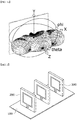
- FIGS. 1A to 1C are views illustrating automotive array antennas according to related arts.
- a conventional automotive array antenna may include a substrate 1, a plurality of monopole antennas or dipole antennas 2, a radio frequency (RF) cable 3, and an RF connector 4.
- RF radio frequency
- a reflecting plate 5 which is disposed at a rear surface is additionally necessary, but it is difficult to mount the reflecting plate inside a bumper of a vehicle due to a large size thereof.
- FIGS. 1B and 1C an emission pattern of an automotive array antenna according to a related art is shown in which it may be seen that signal reception in a large range excluding a rear side of a reflecting plate is available.
- the present invention is directed to providing an automotive array antenna configured to implement ideal signal reception performance with a simple structure.
- One aspect of the present invention provides an automotive array antenna including a first substrate, a plurality of second substrates perpendicularly disposed in one surface of the first substrate to be spaced apart at certain intervals, and a loop antenna formed on one surface of each of the plurality of second substrates.
- the one surfaces of the plurality of second substrates are arranged in the same direction.
- the loop antenna may include a radiator, a feeding line formed to extend from one end of the radiator and connected to a signal line of the first substrate, and a ground line formed to extend from the other end of the radiator and connected to a ground of the first substrate.
- the radiator may be formed to have any one shape of a circular shape, an elliptical shape, and a polygonal shape.
- the first substrate and the second substrate may be integrally formed.
- the second substrate may be detachably coupled to the first substrate.
- a groove portion may be formed in one surface of the first substrate, and a protruding portion inserted into and coupled to the groove portion may be formed on one side of the second substrate.
- the loop antenna may be a monopole antenna.
- an automotive array antenna including a first substrate including a ground formed on one surface, a plurality of second substrates perpendicularly disposed in one surface of the first substrate to be spaced apart at certain intervals, and a loop antenna and ground plane formed on one surface of each of the plurality of second substrates.
- the one surfaces of the plurality of second substrates are arranged in the same direction.
- the one surface of the second substrate may include a first region and a second region.
- the loop antenna may be formed in the first region
- the ground plane connected to the ground of the first substrate may be formed in the second region.
- An emission area may be controllable according to an area of the ground plane.
- the loop antenna may include a radiator, a feeding line formed to extend from one end of the radiator and connected to a signal line of the first substrate, and a ground line formed to extend from the other end of the radiator and connected to the ground plane.
- An entire length of the radiator may be 1 ⁇ , and a ratio between a lateral length and a longitudinal length of the radiator may be formed to be 5:4.
- a ratio between a length of the feeding line and a length of the ground plane may be formed to be 1:1.
- signal reception in a wide range excluding a rear side may be available with a simple structure.
- performance equal to ideal dipole antennas may be implemented.
- a size of an antenna may be easily increased by adjusting the number of the second substrates.
- first, second, A, B, (a), (b), and the like may be used.
- the element may not only be directly connected or coupled to the other element but also be connected or coupled to the other element with another intervening element.
- an element when it is stated that an element is formed or disposed "above or below” another element, the two elements may not only come into direct contact with each other but also still another element may be formed or disposed between the two elements. Also, being “above (on) or below (beneath)” may include not only being in an upward direction but also being in a downward direction on the basis of one element.
- an automotive array antenna having a novel structure in which a plurality of second substrates are perpendicularly arranged at certain intervals on one surface of a first substrate and a loop antenna is formed on one surface of each of the plurality of second substrates.
- the automotive array antenna according to the embodiment may be configured for short-range wireless communication technology-based angle of arrival (AOA) location determination.
- the short-range wireless communication technology may include, for example, Bluetooth low energy (BLE) and the like.
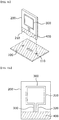
- FIG. 2 is a view illustrating the automotive array antenna according to the first embodiment of the present invention
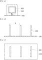
- FIGS. 3A to 3D are views illustrating a shape of the automotive array antenna shown in FIG. 2 .
- the automotive array antenna for location determination may include a first substrate 100, a second substrate 200, and a loop antenna 300.
- a plurality of such second substrates 200 may be perpendicularly arranged on one surface of the first substrate 100 while the plurality of second substrates 200 are spaced at certain intervals.
- the first substrate 100 may be used as a support device for linearly arranging the plurality of second substrates 200 and may also be used as a reflecting device to reflect signals, which are emitted through the loop antennas formed on the plurality of second substrates 200, forward from the one surface.
- the first substrate 100 may be a printed circuit board (PCB) which is a lamination plate covered with copper coil. Accordingly, the first substrate 100 may be a reflecting device using a copper foil film which forms a basic lamination structure without needing to form an additional reflecting device on the one surface.
- PCB printed circuit board
- the second substrates 200 may be perpendicularly arranged on one surface of the first substrate 100 to be spaced apart at certain intervals.
- the loop antenna may be formed on one surface of the second substrate 200.
- the present invention is not limited thereto and two or more second substrates 200 may be disposed on one surface of the first substrate 100 as necessary.
- the second substrate 200 may be a PCB that is a lamination plate covered with copper coil.
- the PCB may be totally applicable regardless of a lamination structure.
- a size of the first substrate 100 may be formed to be larger than a size of the second substrate 200.
- the size of the first substrate 100 may be formed to be, for example, 100 mm ⁇ 60 mm in consideration of an installation space.
- the loop antenna 300 may be formed on one surface of each of the plurality of second substrates 200.
- the loop antenna 300 may be equally formed on one surface of each of plurality of the second substrates 200 but is not limited thereto and may be differently formed as necessary.
- the loop antenna 300 may be implemented to be, for example, a monopole antenna.
- the respective loop antennas 300 formed on one surfaces of the plurality of second substrates 200 are spaced apart at certain intervals and an interval D may satisfy Equation 1 below.
- D ⁇ / 4
- ⁇ c / f
- ⁇ indicates a wavelength
- c indicates a speed of light (3 ⁇ 10 8 )
- f indicates frequency
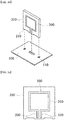
- FIGS. 4A and 4B are views illustrating a coupling relationship between the first substrate and the second substrate which are shown in FIG. 2 .
- the first substrate 100 and the second substrates 200 may be detachably coupled.
- one second substrate 200 will be described.
- one side of the second substrate 200 may be inserted into and coupled to one surface of the first substrate 100.
- a case in which the first substrate 100 and the second substrates 200 are detachably coupled will be described as an example.
- the second substrates 200 may be inserted into and coupled to the first substrate 100 through a dual inline package (DIP) type.
- DIP dual inline package
- the first substrate 100 may include at least one groove portion 110 formed in one surface into which the second substrate 200 is inserted and coupled. Although a case in which three groove portions are formed in one surface of the first substrate 100 is shown, the number of such groove portions is not necessarily limited thereto and may vary as necessary.
- the second substrate 200 may include a protruding portion 210 having one side inserted into and coupled to the at least one groove portion 110 formed in one surface of the first substrate 100. Although a case in which three protruding portions are formed in one surface of the second substrate 200 is shown, the number of such protruding portions is not limited thereto and may vary as necessary.
- the plurality of second substrates 200 may preferably be perpendicularly inserted into and coupled to one surface of the first substrate 100 and arranged to be spaced apart at the same intervals while at least one second substrate may be spaced apart at a different interval as necessary.
- the loop antennas 300 may be formed on one surfaces of the plurality of second substrates 200 while the loop antenna may be formed to be one loop and have the same shape and at least one second substrate may be formed to have a different shape as necessary.
- one surfaces of the plurality of second substrates 200 may be all arranged in the same direction and at least one second substrate may be disposed in a different direction.
- the first substrate 100 and the second substrate 200 may be integrally formed.
- one second substrate 200 will be described.
- the first substrate 100 and the second substrate 200 may be one liquid crystal polymer (LCP) injection material through LCP injection molding.
- LCP liquid crystal polymer
- the loop antenna and a circuit may be formed through a laser direct structuring (LDS) method on the first substrate 100 and the second substrate 200 which are integrally formed.
- LDS laser direct structuring
- FIGS. 5A and 5B are views illustrating a detailed shape of the loop antenna shown in FIG. 2 .
- the loop antenna 300 is formed on one surface of the second substrate 200 according to the embodiment of the present invention.
- the loop antenna 300 may include a radiator 310, a feeding line 320, and a ground line 330.
- the radiator 310 may be formed to have a certain shape to emit a signal and to have, for example, any one shape of a circular shape, an elliptical shape, and a polygonal shape.
- the radiator 310 may be formed of a conductive material, and for example, silver (Ag), palladium (Pd), platinum (Pt), copper (Cu), gold (Au), and nickel (Ni).
- the radiator 310 may be formed to be one loop, the feeding line 320 may be formed to extend from one end of the loop, and the ground line 330 may be formed to extend from the other end of the loop.
- the feeding line 320 and the ground line 330 may be formed to be spaced apart at a certain interval to be parallel.
- the feeding line 320 may be connected to a signal line of the first substrate and the ground line 330 may be connected to a ground of the first substrate.
- the radiator 310 may include one loop while an entire length L of the loop may satisfy 1 ⁇ and a ratio between a lateral length Lx and a longitudinal length Ly of the loop may satisfy 5:4.
- a ratio between a length L_power of the feeding line and a length L_ground of a ground line may satisfy 1:1.
- FIGS. 6A and 6B are views illustrating an emission pattern of the automotive array antenna shown in FIG. 2 .
- a plurality of second substrates which are general low-priced substrates may be perpendicularly arranged on one surface of a first substrate of a certain size and a loop antenna may be formed on one surface of each of the plurality of second substrates so as to have performance equal to that of an existing ideal dipole antenna.
- an automotive array antenna having a novel structure in which a plurality of second substrates are perpendicularly arranged at certain intervals on one surface of a first substrate in which a ground is formed and a loop antenna and a ground plane is formed on one surface of each of the plurality of second substrates.
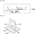
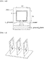
- FIG. 7 is a view illustrating an automotive array antenna according to a second embodiment of the present invention
- FIGS. 8A to 8D are views illustrating a shape of the automotive array antenna shown in FIG. 7 .
- the automotive array antenna for location determination may include a first substrate 100, a second substrate 200, a loop antenna 300, and a ground plane 400.
- the first substrate 100 includes one surface and the other surface.
- a ground may be formed in an overall area of one surface, and a circuit may be formed on the other surface.
- a plurality of such second substrates 200 may be perpendicularly arranged on one surface of the first substrate 100 in which a ground is formed while the plurality of second substrates 200 are spaced at certain intervals.
- the first substrate 100 may be used as a support device for linearly arranging the plurality of second substrates 200 and may be used as a reflecting device to reflect signals emitted through the loop antennas formed on the plurality of second substrates 200 forward from the one surface.
- the first substrate 100 may be a PCB that is a lamination plate covered with copper coil. Accordingly, the first substrate 100 may be a reflecting device using a copper foil film which forms a basic lamination structure without needing to form an additional reflecting device on the one surface.
- the second substrates 200 may be perpendicularly arranged on one surface of the first substrate 100 to be spaced apart at certain intervals.
- the loop antenna may be formed on one surface of the second substrate 200.
- the present invention is not limited thereto and two or more second substrate 200 may be disposed on one surface of the first substrate 100 as necessary.
- the second substrate 200 may be a PCB that is a lamination plate covered with copper coil.
- the PCB may be totally applicable regardless of a lamination structure.
- a size of the first substrate 100 may be formed to be larger than a size of the second substrate 200.
- the size of the first substrate 100 may be formed to be, for example, 100 mm ⁇ 60 mm in consideration of an installation space.
- the loop antenna 300 may be equally formed in a first region of one surface of each of the plurality of second substrates 200.
- the loop antenna 300 may be equally formed on one surface of each of the second substrates 200 but is not limited thereto and may be differently formed as necessary.
- the loop antenna 300 may be implemented to be, for example, a monopole antenna.
- the ground plane 400 may be equally formed in a second region of one surface of each of the plurality of second substrates 200.
- the ground plane 400 may ground the loop antenna 300 while one side thereof may be connected to the loop antenna 300 and the other side may be connected to the ground of the first substrate 100.
- FIGS. 9A and 9B are views illustrating a coupling relationship between the first substrate and the second substrate which are shown in FIG. 7 .
- the first substrate 100 and the second substrate 200 may be integrally formed.
- one second substrate 200 will be described.
- the first substrate 100 and the second substrate 200 may be one LCP injection material through LCP injection molding.
- the loop antenna and a circuit may be formed through an LDS method on the first substrate 100 and the second substrate 200 which are integrally formed. That is, the loop antenna may be formed on the second substrate 200, and the circuit may be formed on the first substrate 100.
- the first substrate and the second substrate are integrally formed will be described as an example.
- the first substrate 100 and the second substrate 200 according to the embodiment may be detachably coupled.
- one second substrate 200 will be described.
- one side of the second substrate 200 may be inserted into and coupled to one surface of the first substrate 100.
- the second substrates 200 may be inserted into and coupled to the first substrate 100 through a DIP type.
- the first substrate 100 may include at least one groove portion 110 formed in one surface into which the second substrate 200 is inserted and coupled.
- the number of such groove portions is not necessarily limited thereto and may vary as necessary.
- the second substrate 200 may include a protruding portion having one side inserted into and coupled to the at least one groove portion formed in one surface of the first substrate.
- a protruding portion having one side inserted into and coupled to the at least one groove portion formed in one surface of the first substrate.
- the number of such protruding portions is not limited thereto and may vary as necessary.
- the plurality of second substrates 200 may preferably be perpendicularly inserted into and coupled to one surface of the first substrate 100 and arranged to be spaced apart at the same intervals while at least one second substrate may be spaced apart at a different interval as necessary.
- the loop antennas 300 may be formed in the first regions of one surfaces of the plurality of second substrates 200 while the loop antenna may be formed to be one loop and have the same shape and at least one second substrate may be formed to have a different shape as necessary.
- ground planes 400 may be formed in the second regions of the one surfaces of the plurality of second substrates 200 while an emission area may be controllable according to an area of the ground plane 400.
- one surfaces of the plurality of second substrates 200 may be all arranged in the same direction and at least one second substrate may be disposed in a different direction.
- FIGS. 10A and 10B are views illustrating a detailed shape of the second substrate shown in FIG. 7 .
- the one surface of the second substrate 200 may include the first region and the second region while the loop antenna 300 may be formed in the first region and the ground plane 400 may be formed in the second region.
- the loop antenna 300 may include the radiator 310, the feeding line 320, and the ground line 330.
- the radiator 310 may be formed to have a certain shape to emit a signal and to have, for example, any one shape of a circular shape, an elliptical shape, and a polygonal shape.
- the radiator 310 may be formed of a conductive material, and for example, Ag, Pd, Pt, Cu, Au, and Ni.
- the radiator 310 may be formed to be one loop, the feeding line 320 may be formed to extend from one end of the loop, and the ground line 330 may be formed to extend from the other end of the loop.
- the feeding line 320 and the ground line 330 may be formed to be spaced apart at a certain interval to be parallel.
- the feeding line 320 may be connected to a signal line of the first substrate, and the ground line 330 may be connected to the ground plane 400.
- An emission area may be controllable according to an area of the ground plane 400. That is, as the area, in detail, a height h, of the ground plane 400 increases, the emission area may be further increased.
- the radiator 310 may include one loop while an entire length L of the loop may satisfy 1 ⁇ and a ratio between a lateral length Lx and a longitudinal length Ly of the loop may satisfy 5:4.
- a ratio between a length L_power of the feeding line and a length L_ground of a ground line may satisfy 1:1.
- a ratio between a length L_power of the feeding line and a length L_ground_plane of a ground plane may satisfy 1:1.
- the length L_power of the feeding line and the length L_ground_plane of the ground plane may be 10 mm.
- FIGS. 11A and 11B are views illustrating an emission pattern of the automotive array antenna shown in FIG. 7 .
- a plurality of second substrates which are general low-priced substrates may be perpendicularly arranged on one surface of a first substrate of a certain size and a loop antenna and a ground plane may be formed on one surface of the second substrate so as to have performance equal to that of an existing ideal dipole antenna.
- FIGS. 12A and 12B are views illustrating an emission pattern of an automotive array antenna mounted in a vehicle.
- the automotive array antenna according to the first embodiment or the second embodiment of the present invention may be installed on each of both end portions P1, P2, P3, and P4 of both a front bumper and a rear bumper to perform BLE AOA location determination in the vehicle. Since doors or the like of the vehicle are formed of metal, mounting is difficult. A shark antenna is already saturated, and thus it is impossible to place several linear antennas in a band of 2.4 GHz.
- the automotive array antennas When the automotive array antennas are located on the front bumper and the rear bumper of the vehicle, it is significant to allow waveforms of the antenna to be emitted outward from the vehicle. Accordingly, since the plurality of second substrates are perpendicularly arranged on one surface of the first substrate having a certain size so as to allow the first substrate to function as a reflecting plate like the embodiment, signals may be evenly emitted.
- the antenna according to the embodiment may satisfy antenna performance only using a low-priced substrate FR-4.
- antennas are installed at four locations in a vehicle
- the present invention is not limited thereto, and installation locations and number may be varied as necessary.
Landscapes
- Engineering & Computer Science (AREA)
- Computer Security & Cryptography (AREA)
- Radar, Positioning & Navigation (AREA)
- Remote Sensing (AREA)
- Details Of Aerials (AREA)
- Variable-Direction Aerials And Aerial Arrays (AREA)
Abstract
Description
- The present invention relates to a location determination technique, and more particularly, to an automotive array antenna configured to implement ideal signal reception performance with a simple structure.
- In order to compensate for disadvantages of a smart key that has vulnerable security, alternative techniques have been vigorously developed by companies related to vehicles in Korea, Japan, the U.S.A., and the like. As representative alternative techniques, there are near field communication (NFC) and Bluetooth low energy (BLE) technologies. NFC has a distance inconvenience of having to bring a phone into contact with a vehicle, and a BLE vehicle location determination technique is improved therefrom one stage further. To determine a location, a location of a cell phone is calculated by detecting a phase difference between signals transmitted and received after respective antennas are spaced apart at certain intervals or more.
- To add a BLE angle of arrival (AOA) function to a vehicle, it is necessary to recognize a user's phone in a full range of a vehicle and an antenna array technique is most significant therein. Here, for transmission and reception with the phone, it is necessary to evenly increase an emission range of each antenna.
-
FIGS. 1A to 1C are views illustrating automotive array antennas according to related arts. - Referring to
FIG. 1A , a conventional automotive array antenna may include asubstrate 1, a plurality of monopole antennas ordipole antennas 2, a radio frequency (RF)cable 3, and anRF connector 4. Here, since such monopole antennas or dipole antennas are expensive and three RF cables and six RF connectors are necessary when three antennas are used, costs increase. - Also, due to a linear array structure, a reflecting
plate 5 which is disposed at a rear surface is additionally necessary, but it is difficult to mount the reflecting plate inside a bumper of a vehicle due to a large size thereof. - Referring to
FIGS. 1B and1C , an emission pattern of an automotive array antenna according to a related art is shown in which it may be seen that signal reception in a large range excluding a rear side of a reflecting plate is available. - However, when an array antenna is designed to increase an emission range of each antenna, the array antenna increases in size and cost, and actually, there is no space in a vehicle to place the array antenna. Until now, only ideal antennas with no substantial ability to be mass produced have been designed.
-
Korean Patent Publication No. 10-2017-0026255 - The present invention is directed to providing an automotive array antenna configured to implement ideal signal reception performance with a simple structure.
- One aspect of the present invention provides an automotive array antenna including a first substrate, a plurality of second substrates perpendicularly disposed in one surface of the first substrate to be spaced apart at certain intervals, and a loop antenna formed on one surface of each of the plurality of second substrates. Here, the one surfaces of the plurality of second substrates are arranged in the same direction.
- The loop antenna may include a radiator, a feeding line formed to extend from one end of the radiator and connected to a signal line of the first substrate, and a ground line formed to extend from the other end of the radiator and connected to a ground of the first substrate.
- The radiator may be formed to have any one shape of a circular shape, an elliptical shape, and a polygonal shape.
- The first substrate and the second substrate may be integrally formed.
- The second substrate may be detachably coupled to the first substrate. A groove portion may be formed in one surface of the first substrate, and a protruding portion inserted into and coupled to the groove portion may be formed on one side of the second substrate.
- The loop antenna may be a monopole antenna.
- Another aspect of the present invention provides an automotive array antenna including a first substrate including a ground formed on one surface, a plurality of second substrates perpendicularly disposed in one surface of the first substrate to be spaced apart at certain intervals, and a loop antenna and ground plane formed on one surface of each of the plurality of second substrates. Here, the one surfaces of the plurality of second substrates are arranged in the same direction.
- The one surface of the second substrate may include a first region and a second region. Here, the loop antenna may be formed in the first region, and the ground plane connected to the ground of the first substrate may be formed in the second region.
- An emission area may be controllable according to an area of the ground plane.
- The loop antenna may include a radiator, a feeding line formed to extend from one end of the radiator and connected to a signal line of the first substrate, and a ground line formed to extend from the other end of the radiator and connected to the ground plane.
- An entire length of the radiator may be 1 λ, and a ratio between a lateral length and a longitudinal length of the radiator may be formed to be 5:4.
- A ratio between a length of the feeding line and a length of the ground plane may be formed to be 1:1.
- According to embodiments, signal reception in a wide range excluding a rear side may be available with a simple structure.
- According to embodiments, even with a simple structure, performance equal to ideal dipole antennas may be implemented.
- According to embodiments, since a low-priced substrate is used and high-priced dipole antennas, cables, and connectors are not used, material costs may be significantly reduced and miniaturization may be available.
- According to embodiments, since a plurality of second substrates are perpendicularly arranged at certain intervals on one surface of a first substrate, a size of an antenna may be easily increased by adjusting the number of the second substrates.
-
-
FIGS. 1A to 1C are views illustrating automotive array antennas according to related arts. -
FIG. 2 is a view illustrating an automotive array antenna according to a first embodiment of the present invention. -
FIGS. 3A to 3D are views illustrating a shape of the automotive array antenna shown inFIG. 2 . -
FIGS. 4A and4B are views illustrating a coupling relationship between a first substrate and a second substrate which are shown inFIG. 2 . -
FIGS. 5A and5B are views illustrating a detailed shape of a loop antenna shown inFIG. 2 . -
FIGS. 6A and6B are views illustrating an emission pattern of the automotive array antenna shown inFIG. 2 . -
FIG. 7 is a view illustrating an automotive array antenna according to a second embodiment of the present invention. -
FIGS. 8A to 8D are views illustrating a shape of the automotive array antenna shown inFIG. 7 . -
FIGS. 9A and9B are views illustrating a coupling relationship between a first substrate and a second substrate which are shown inFIG. 7 . -
FIGS. 10A and10B are views illustrating a detailed shape of the second substrate shown inFIG. 7 . -
FIGS. 11A and11B are views illustrating an emission pattern of the automotive array antenna shown inFIG. 7 . -
FIGS. 12A and12B are views illustrating an emission pattern of an automotive array antenna mounted in a vehicle. - Hereinafter, exemplary embodiments of the present invention will be described in detail with reference to the drawings.
- However, the technical concept of the present invention is not limited to some embodiments disclosed below but can be implemented in a variety of different forms. One or more of components of the embodiments may be selectively combined or substituted with one another without departing from the scope of the technical concept of the present invention.
- Also, unless defined otherwise, the terms (including technical and scientific terms) used herein may be used as meanings capable of being commonly understood by one of ordinary skill in the art. Also, terms defined in generally used dictionaries may be construed in consideration of the contextual meanings of the related art.
- Also, the terms used herein are intended to describe the embodiments but not intended to restrict the present invention.
- Throughout the specification, unless stated otherwise particularly, singular forms include plural forms. When at least one (or one or more) of A, B, and C is stated, this may include one or more of all combinations of A, B, and C.
- Also, in describing components of the embodiments of the present invention, the terms such as first, second, A, B, (a), (b), and the like may be used.
- These terms are merely for distinguishing one element from another, and the essential, order, sequence, and the like of corresponding elements are not limited by the terms.
- Also, when it is stated that one element is "connected," or "coupled" to another, the element may not only be directly connected or coupled to the other element but also be connected or coupled to the other element with another intervening element.
- Also, when it is stated that an element is formed or disposed "above or below" another element, the two elements may not only come into direct contact with each other but also still another element may be formed or disposed between the two elements. Also, being "above (on) or below (beneath)" may include not only being in an upward direction but also being in a downward direction on the basis of one element.
- In a first embodiment, there is provided an automotive array antenna having a novel structure in which a plurality of second substrates are perpendicularly arranged at certain intervals on one surface of a first substrate and a loop antenna is formed on one surface of each of the plurality of second substrates. Particularly, the automotive array antenna according to the embodiment may be configured for short-range wireless communication technology-based angle of arrival (AOA) location determination. Here, the short-range wireless communication technology may include, for example, Bluetooth low energy (BLE) and the like.
-
FIG. 2 is a view illustrating the automotive array antenna according to the first embodiment of the present invention, andFIGS. 3A to 3D are views illustrating a shape of the automotive array antenna shown inFIG. 2 . - Referring to
FIGS. 2 and3A to 3D , the automotive array antenna for location determination according to the first embodiment of the present invention may include afirst substrate 100, asecond substrate 200, and aloop antenna 300. - A plurality of such
second substrates 200 may be perpendicularly arranged on one surface of thefirst substrate 100 while the plurality ofsecond substrates 200 are spaced at certain intervals. Thefirst substrate 100 may be used as a support device for linearly arranging the plurality ofsecond substrates 200 and may also be used as a reflecting device to reflect signals, which are emitted through the loop antennas formed on the plurality ofsecond substrates 200, forward from the one surface. - The
first substrate 100 may be a printed circuit board (PCB) which is a lamination plate covered with copper coil. Accordingly, thefirst substrate 100 may be a reflecting device using a copper foil film which forms a basic lamination structure without needing to form an additional reflecting device on the one surface. - The
second substrates 200 may be perpendicularly arranged on one surface of thefirst substrate 100 to be spaced apart at certain intervals. The loop antenna may be formed on one surface of thesecond substrate 200. In the embodiment, although it has been described as an example that threesecond substrates 200 are disposed on one surface of thefirst substrate 100, the present invention is not limited thereto and two or moresecond substrates 200 may be disposed on one surface of thefirst substrate 100 as necessary. - The
second substrate 200 may be a PCB that is a lamination plate covered with copper coil. Here, the PCB may be totally applicable regardless of a lamination structure. - Here, a size of the
first substrate 100 may be formed to be larger than a size of thesecond substrate 200. The size of thefirst substrate 100 may be formed to be, for example, 100 mm×60 mm in consideration of an installation space. - The
loop antenna 300 may be formed on one surface of each of the plurality ofsecond substrates 200. Theloop antenna 300 may be equally formed on one surface of each of plurality of thesecond substrates 200 but is not limited thereto and may be differently formed as necessary. - The
loop antenna 300 may be implemented to be, for example, a monopole antenna. - Here, the
respective loop antennas 300 formed on one surfaces of the plurality ofsecond substrates 200 are spaced apart at certain intervals and an interval D may satisfyEquation 1 below.
- Here, λ indicates a wavelength, c indicates a speed of light (3×10⁸), and f indicates frequency.
-
FIGS. 4A and4B are views illustrating a coupling relationship between the first substrate and the second substrate which are shown inFIG. 2 . - Referring to
FIG. 4A , thefirst substrate 100 and thesecond substrates 200 according to the embodiment may be detachably coupled. Here, for convenience of description, onesecond substrate 200 will be described. For example, one side of thesecond substrate 200 may be inserted into and coupled to one surface of thefirst substrate 100. In the embodiment, a case in which thefirst substrate 100 and thesecond substrates 200 are detachably coupled will be described as an example. - As described above, the
second substrates 200 may be inserted into and coupled to thefirst substrate 100 through a dual inline package (DIP) type. - To this end, the
first substrate 100 may include at least onegroove portion 110 formed in one surface into which thesecond substrate 200 is inserted and coupled. Although a case in which three groove portions are formed in one surface of thefirst substrate 100 is shown, the number of such groove portions is not necessarily limited thereto and may vary as necessary. - The
second substrate 200 may include a protrudingportion 210 having one side inserted into and coupled to the at least onegroove portion 110 formed in one surface of thefirst substrate 100. Although a case in which three protruding portions are formed in one surface of thesecond substrate 200 is shown, the number of such protruding portions is not limited thereto and may vary as necessary. - Here, the plurality of
second substrates 200 may preferably be perpendicularly inserted into and coupled to one surface of thefirst substrate 100 and arranged to be spaced apart at the same intervals while at least one second substrate may be spaced apart at a different interval as necessary. - Also, the
loop antennas 300 may be formed on one surfaces of the plurality ofsecond substrates 200 while the loop antenna may be formed to be one loop and have the same shape and at least one second substrate may be formed to have a different shape as necessary. - Also, one surfaces of the plurality of
second substrates 200 may be all arranged in the same direction and at least one second substrate may be disposed in a different direction. - Referring to
FIG. 4B , thefirst substrate 100 and thesecond substrate 200 according to the embodiment may be integrally formed. Here, for convenience of description, onesecond substrate 200 will be described. For example, thefirst substrate 100 and thesecond substrate 200 may be one liquid crystal polymer (LCP) injection material through LCP injection molding. - Subsequently, the loop antenna and a circuit may be formed through a laser direct structuring (LDS) method on the
first substrate 100 and thesecond substrate 200 which are integrally formed. -
FIGS. 5A and5B are views illustrating a detailed shape of the loop antenna shown inFIG. 2 . - Referring to
FIGS. 5A and5B , theloop antenna 300 is formed on one surface of thesecond substrate 200 according to the embodiment of the present invention. Theloop antenna 300 may include aradiator 310, afeeding line 320, and aground line 330. - The
radiator 310 may be formed to have a certain shape to emit a signal and to have, for example, any one shape of a circular shape, an elliptical shape, and a polygonal shape. Here, theradiator 310 may be formed of a conductive material, and for example, silver (Ag), palladium (Pd), platinum (Pt), copper (Cu), gold (Au), and nickel (Ni). - The
radiator 310 may be formed to be one loop, thefeeding line 320 may be formed to extend from one end of the loop, and theground line 330 may be formed to extend from the other end of the loop. Thefeeding line 320 and theground line 330 may be formed to be spaced apart at a certain interval to be parallel. - Here, when the second substrate is inserted into and coupled to the first substrate, the
feeding line 320 may be connected to a signal line of the first substrate and theground line 330 may be connected to a ground of the first substrate. - Also, the
radiator 310 may include one loop while an entire length L of the loop may satisfy 1 λ and a ratio between a lateral length Lx and a longitudinal length Ly of the loop may satisfy 5:4. - Also, a ratio between a length L_power of the feeding line and a length L_ground of a ground line may satisfy 1:1.
-
FIGS. 6A and6B are views illustrating an emission pattern of the automotive array antenna shown inFIG. 2 . - Referring to
FIGS. 6A and6B , in the embodiment, it may be seen through a computer simulation that a plurality of second substrates which are general low-priced substrates may be perpendicularly arranged on one surface of a first substrate of a certain size and a loop antenna may be formed on one surface of each of the plurality of second substrates so as to have performance equal to that of an existing ideal dipole antenna. - In a second embodiment, there is provided an automotive array antenna having a novel structure in which a plurality of second substrates are perpendicularly arranged at certain intervals on one surface of a first substrate in which a ground is formed and a loop antenna and a ground plane is formed on one surface of each of the plurality of second substrates.
-
FIG. 7 is a view illustrating an automotive array antenna according to a second embodiment of the present invention, andFIGS. 8A to 8D are views illustrating a shape of the automotive array antenna shown inFIG. 7 . - Referring to
FIGS. 7 and8A to 8D , the automotive array antenna for location determination according to the second embodiment of the present invention may include afirst substrate 100, asecond substrate 200, aloop antenna 300, and aground plane 400. - The
first substrate 100 includes one surface and the other surface. A ground may be formed in an overall area of one surface, and a circuit may be formed on the other surface. A plurality of suchsecond substrates 200 may be perpendicularly arranged on one surface of thefirst substrate 100 in which a ground is formed while the plurality ofsecond substrates 200 are spaced at certain intervals. Thefirst substrate 100 may be used as a support device for linearly arranging the plurality ofsecond substrates 200 and may be used as a reflecting device to reflect signals emitted through the loop antennas formed on the plurality ofsecond substrates 200 forward from the one surface. - The
first substrate 100 may be a PCB that is a lamination plate covered with copper coil. Accordingly, thefirst substrate 100 may be a reflecting device using a copper foil film which forms a basic lamination structure without needing to form an additional reflecting device on the one surface. - The
second substrates 200 may be perpendicularly arranged on one surface of thefirst substrate 100 to be spaced apart at certain intervals. The loop antenna may be formed on one surface of thesecond substrate 200. In the embodiment, although it has been described as an example that threesecond substrates 200 are disposed on one surface of thefirst substrate 100, the present invention is not limited thereto and two or moresecond substrate 200 may be disposed on one surface of thefirst substrate 100 as necessary. - The
second substrate 200 may be a PCB that is a lamination plate covered with copper coil. Here, the PCB may be totally applicable regardless of a lamination structure. - Here, a size of the
first substrate 100 may be formed to be larger than a size of thesecond substrate 200. The size of thefirst substrate 100 may be formed to be, for example, 100 mm×60 mm in consideration of an installation space. - The
loop antenna 300 may be equally formed in a first region of one surface of each of the plurality ofsecond substrates 200. Theloop antenna 300 may be equally formed on one surface of each of thesecond substrates 200 but is not limited thereto and may be differently formed as necessary. - The
loop antenna 300 may be implemented to be, for example, a monopole antenna. - The
ground plane 400 may be equally formed in a second region of one surface of each of the plurality ofsecond substrates 200. Theground plane 400 may ground theloop antenna 300 while one side thereof may be connected to theloop antenna 300 and the other side may be connected to the ground of thefirst substrate 100. -
FIGS. 9A and9B are views illustrating a coupling relationship between the first substrate and the second substrate which are shown inFIG. 7 . - Referring to
FIG. 9A , thefirst substrate 100 and thesecond substrate 200 according to the embodiment may be integrally formed. Here, for convenience of description, onesecond substrate 200 will be described. For example, thefirst substrate 100 and thesecond substrate 200 may be one LCP injection material through LCP injection molding. - Subsequently, the loop antenna and a circuit may be formed through an LDS method on the
first substrate 100 and thesecond substrate 200 which are integrally formed. That is, the loop antenna may be formed on thesecond substrate 200, and the circuit may be formed on thefirst substrate 100. In the embodiment, a case in which the first substrate and the second substrate are integrally formed will be described as an example. - Referring to
FIG. 9B , thefirst substrate 100 and thesecond substrate 200 according to the embodiment may be detachably coupled. Here, for convenience of description, onesecond substrate 200 will be described. For example, one side of thesecond substrate 200 may be inserted into and coupled to one surface of thefirst substrate 100. - As described above, the
second substrates 200 may be inserted into and coupled to thefirst substrate 100 through a DIP type. - To this end, the
first substrate 100 may include at least onegroove portion 110 formed in one surface into which thesecond substrate 200 is inserted and coupled. In the embodiment, although a case in which three groove portions are formed in one surface of thefirst substrate 100 is shown, the number of such groove portions is not necessarily limited thereto and may vary as necessary. - The
second substrate 200 may include a protruding portion having one side inserted into and coupled to the at least one groove portion formed in one surface of the first substrate. In the embodiment, although a case in which three protruding portions are formed in one surface of thesecond substrate 200 is shown, the number of such protruding portions is not limited thereto and may vary as necessary. - Here, the plurality of
second substrates 200 may preferably be perpendicularly inserted into and coupled to one surface of thefirst substrate 100 and arranged to be spaced apart at the same intervals while at least one second substrate may be spaced apart at a different interval as necessary. - Also, the
loop antennas 300 may be formed in the first regions of one surfaces of the plurality ofsecond substrates 200 while the loop antenna may be formed to be one loop and have the same shape and at least one second substrate may be formed to have a different shape as necessary. - Also, the ground planes 400 may be formed in the second regions of the one surfaces of the plurality of
second substrates 200 while an emission area may be controllable according to an area of theground plane 400. - Also, one surfaces of the plurality of
second substrates 200 may be all arranged in the same direction and at least one second substrate may be disposed in a different direction. -
FIGS. 10A and10B are views illustrating a detailed shape of the second substrate shown inFIG. 7 . - Referring to
FIGS. 10A and10B , the one surface of thesecond substrate 200 according to the embodiment may include the first region and the second region while theloop antenna 300 may be formed in the first region and theground plane 400 may be formed in the second region. - The
loop antenna 300 may include theradiator 310, thefeeding line 320, and theground line 330. - The
radiator 310 may be formed to have a certain shape to emit a signal and to have, for example, any one shape of a circular shape, an elliptical shape, and a polygonal shape. Here, theradiator 310 may be formed of a conductive material, and for example, Ag, Pd, Pt, Cu, Au, and Ni. - The
radiator 310 may be formed to be one loop, thefeeding line 320 may be formed to extend from one end of the loop, and theground line 330 may be formed to extend from the other end of the loop. Thefeeding line 320 and theground line 330 may be formed to be spaced apart at a certain interval to be parallel. - The
feeding line 320 may be connected to a signal line of the first substrate, and theground line 330 may be connected to theground plane 400. - An emission area may be controllable according to an area of the
ground plane 400. That is, as the area, in detail, a height h, of theground plane 400 increases, the emission area may be further increased. - Here, the
radiator 310 may include one loop while an entire length L of the loop may satisfy 1 λ and a ratio between a lateral length Lx and a longitudinal length Ly of the loop may satisfy 5:4. - Also, a ratio between a length L_power of the feeding line and a length L_ground of a ground line may satisfy 1:1.
- Also, a ratio between a length L_power of the feeding line and a length L_ground_plane of a ground plane may satisfy 1:1. For example, the length L_power of the feeding line and the length L_ground_plane of the ground plane may be 10 mm.
-
FIGS. 11A and11B are views illustrating an emission pattern of the automotive array antenna shown inFIG. 7 . - Referring to
FIGS. 11A and11B , in the embodiment, it may be seen through a computer simulation that a plurality of second substrates which are general low-priced substrates may be perpendicularly arranged on one surface of a first substrate of a certain size and a loop antenna and a ground plane may be formed on one surface of the second substrate so as to have performance equal to that of an existing ideal dipole antenna. -
FIGS. 12A and12B are views illustrating an emission pattern of an automotive array antenna mounted in a vehicle. - Referring to
FIGS. 12A and12B , the automotive array antenna according to the first embodiment or the second embodiment of the present invention may be installed on each of both end portions P1, P2, P3, and P4 of both a front bumper and a rear bumper to perform BLE AOA location determination in the vehicle. Since doors or the like of the vehicle are formed of metal, mounting is difficult. A shark antenna is already saturated, and thus it is impossible to place several linear antennas in a band of 2.4 GHz. - When the automotive array antennas are located on the front bumper and the rear bumper of the vehicle, it is significant to allow waveforms of the antenna to be emitted outward from the vehicle. Accordingly, since the plurality of second substrates are perpendicularly arranged on one surface of the first substrate having a certain size so as to allow the first substrate to function as a reflecting plate like the embodiment, signals may be evenly emitted.
- Accordingly, unlike a method of using a plurality of existing high-priced antennas and a plurality of RF cables, the antenna according to the embodiment may satisfy antenna performance only using a low-priced substrate FR-4.
- Here, although a case in which antennas are installed at four locations in a vehicle is described as an example, the present invention is not limited thereto, and installation locations and number may be varied as necessary.
- Although the exemplary embodiments of the present invention have been described above, it may be understood by those skilled in the art that a variety of modifications and changes may be made without departing from the concept and scope of the present invention disclosed within the range of the following claims.
Claims (10)
- An automotive array antenna comprising:a first substrate;a plurality of second substrates perpendicularly disposed in one surface of the first substrate to be spaced apart at certain intervals; anda loop antenna formed on one surface of each of the plurality of second substrates,wherein the one surfaces of the plurality of second substrates are arranged in the same direction.
- The automotive array antenna of claim 1, wherein the loop antenna comprises:a radiator;a feeding line formed to extend from one end of the radiator and connected to a signal line of the first substrate; anda ground line formed to extend from the other end of the radiator and connected to a ground of the first substrate.
- The automotive array antenna of claim 1, wherein the first substrate and the second substrate are integrally formed.
- The automotive array antenna of claim 1, wherein the second substrate is detachably coupled to the first substrate,wherein a groove portion is formed in one surface of the first substrate, andwherein a protruding portion inserted into and coupled to the groove portion is formed on one side of the second substrate.
- An automotive array antenna comprising:a first substrate comprising a ground formed on one surface;a plurality of second substrates perpendicularly disposed in one surface of the first substrate to be spaced apart at certain intervals; anda loop antenna and ground plane formed on one surface of each of the plurality of second substrates,wherein the one surfaces of the plurality of second substrates are arranged in the same direction.
- The automotive array antenna of claim 5, wherein the one surface of the second substrate comprises a first region and a second region,wherein the loop antenna is formed in the first region, andwherein the ground plane connected to the ground of the first substrate is formed in the second region.
- The automotive array antenna of claim 6, wherein an emission area is controllable according to an area of the ground plane.
- The automotive array antenna of claim 5, wherein the loop antenna comprises:a radiator;a feeding line formed to extend from one end of the radiator and connected to a signal line of the first substrate; anda ground line formed to extend from the other end of the radiator and connected to the ground plane.
- The automotive array antenna of claim 8, wherein an entire length of the radiator is 1 λ, and
wherein a ratio between a lateral length and a longitudinal length of the radiator is formed to be 5:4. - The automotive array antenna of claim 8, wherein a ratio between a length of the feeding line and a length of the ground plane is formed to be 1:1.
Applications Claiming Priority (3)
| Application Number | Priority Date | Filing Date | Title |
|---|---|---|---|
| KR1020190000679A KR102670667B1 (en) | 2019-01-03 | 2019-01-03 | Array antenna for vehicle |
| KR1020190000573A KR102670675B1 (en) | 2019-01-03 | 2019-01-03 | Array antenna for vehicle |
| PCT/KR2020/000079 WO2020141918A1 (en) | 2019-01-03 | 2020-01-03 | Automotive array antenna |
Publications (4)
| Publication Number | Publication Date |
|---|---|
| EP3907822A1 true EP3907822A1 (en) | 2021-11-10 |
| EP3907822A4 EP3907822A4 (en) | 2022-10-05 |
| EP3907822B1 EP3907822B1 (en) | 2026-03-04 |
| EP3907822B9 EP3907822B9 (en) | 2026-05-27 |
Family
ID=71406617
Family Applications (1)
| Application Number | Title | Priority Date | Filing Date |
|---|---|---|---|
| EP20735856.5A Active EP3907822B9 (en) | 2019-01-03 | 2020-01-03 | Automotive array antenna |
Country Status (5)
| Country | Link |
|---|---|
| US (1) | US11978951B2 (en) |
| EP (1) | EP3907822B9 (en) |
| JP (1) | JP7506675B2 (en) |
| CN (1) | CN113302797A (en) |
| WO (1) | WO2020141918A1 (en) |
Families Citing this family (1)
| Publication number | Priority date | Publication date | Assignee | Title |
|---|---|---|---|---|
| US11342678B1 (en) * | 2020-11-17 | 2022-05-24 | Malathi K | Dual polarized MIMO UWB system: a method and device thereof |
Family Cites Families (18)
| Publication number | Priority date | Publication date | Assignee | Title |
|---|---|---|---|---|
| US6359596B1 (en) * | 2000-07-28 | 2002-03-19 | Lockheed Martin Corporation | Integrated circuit mm-wave antenna structure |
| KR100738166B1 (en) | 2003-01-08 | 2007-07-10 | 가부시키가이샤 고쿠사이 덴키 츠신 기소 기주츠 겐큐쇼 | Array antenna control device and array antenna device |
| KR101066378B1 (en) | 2003-02-03 | 2011-09-20 | 파나소닉 주식회사 | Antenna device using micro loop antenna and wireless communication device using antenna device |
| JP4560480B2 (en) | 2005-12-13 | 2010-10-13 | Necトーキン株式会社 | Wireless tag |
| US7969372B2 (en) | 2006-08-03 | 2011-06-28 | Panasonic Corporation | Antenna apparatus utilizing small loop antenna element having minute length and two feeding points |
| KR20100056446A (en) * | 2007-08-03 | 2010-05-27 | 파나소닉 주식회사 | Antenna device |
| JP5162394B2 (en) | 2008-09-25 | 2013-03-13 | パナソニック株式会社 | Antenna device |
| JP2012116576A (en) | 2010-11-29 | 2012-06-21 | Nippon Sheet Glass Co Ltd | Disk mounting shelf and disk management system |
| WO2012072969A1 (en) | 2010-11-29 | 2012-06-07 | The University Of Birmingham | Balanced antenna system |
| KR20130112518A (en) * | 2012-04-04 | 2013-10-14 | 엘에스전선 주식회사 | Dual polarization dipole antenna for broad-band and antenna array using it |
| US9252501B2 (en) | 2012-05-28 | 2016-02-02 | North Carolina State University | Millimeter scale three-dimensional antenna structures and methods for fabricating same |
| KR20130134793A (en) * | 2012-05-31 | 2013-12-10 | 엘에스전선 주식회사 | Dual polarization dipole antenna for dual-band and antenna array using it |
| EP2833479B1 (en) * | 2013-08-02 | 2020-03-18 | Advanced Automotive Antennas, S.L. | Antenna system for a vehicle |
| JP2017041661A (en) * | 2014-01-14 | 2017-02-23 | アルプス電気株式会社 | Antenna device |
| US9496614B2 (en) | 2014-04-15 | 2016-11-15 | Dockon Ag | Antenna system using capacitively coupled compound loop antennas with antenna isolation provision |
| JP5872018B1 (en) | 2014-12-19 | 2016-03-01 | 電気興業株式会社 | Dual-polarized antenna device |
| US10784588B2 (en) * | 2014-12-19 | 2020-09-22 | Saab Ab | Surface mounted broadband element |
| FR3040551B1 (en) | 2015-08-28 | 2018-08-17 | Continental Automotive France | METHOD FOR ULTRA HIGH FREQUENCY LOCALIZATION OF A PORTABLE "HAND FREE" ACCESS DEVICE TO A MOTOR VEHICLE AND ASSOCIATED LOCATION DEVICE |
-
2020
- 2020-01-03 CN CN202080007800.XA patent/CN113302797A/en active Pending
- 2020-01-03 US US17/419,539 patent/US11978951B2/en active Active
- 2020-01-03 EP EP20735856.5A patent/EP3907822B9/en active Active
- 2020-01-03 JP JP2021538806A patent/JP7506675B2/en active Active
- 2020-01-03 WO PCT/KR2020/000079 patent/WO2020141918A1/en not_active Ceased
Also Published As
| Publication number | Publication date |
|---|---|
| WO2020141918A1 (en) | 2020-07-09 |
| EP3907822A4 (en) | 2022-10-05 |
| CN113302797A (en) | 2021-08-24 |
| EP3907822B1 (en) | 2026-03-04 |
| JP7506675B2 (en) | 2024-06-26 |
| JP2022516912A (en) | 2022-03-03 |
| US20220077575A1 (en) | 2022-03-10 |
| EP3907822B9 (en) | 2026-05-27 |
| US11978951B2 (en) | 2024-05-07 |
Similar Documents
| Publication | Publication Date | Title |
|---|---|---|
| US7289068B2 (en) | Planar antenna with multiple radiators and notched ground pattern | |
| CN1047473C (en) | Folding dipole antenna | |
| US7079079B2 (en) | Low profile compact multi-band meanderline loaded antenna | |
| EP1493204B1 (en) | Multi-band planar antenna | |
| US20110090131A1 (en) | Printed Dual-Band Yagi-Uda Antenna and Circular Polarization Antenna | |
| EP2928020A1 (en) | Antenna for mobile-communication base station | |
| EP3465823B1 (en) | C-fed antenna formed on multi-layer printed circuit board edge | |
| EP1944828A2 (en) | Planar antenna | |
| WO2012102576A2 (en) | Broad-band dual polarization dipole antenna and antenna array | |
| JP2006517074A (en) | Multi-antenna diversity in mobile phone handsets, PDAs and other electrical miniature wireless platforms | |
| US20080068276A1 (en) | Antenna device | |
| KR100732666B1 (en) | Mobile communication terminal equipped with a plurality of antennas | |
| KR102670667B1 (en) | Array antenna for vehicle | |
| EP1950831A1 (en) | Dipole array directional antenna | |
| EP3907822B1 (en) | Automotive array antenna | |
| US7180461B2 (en) | Wideband omnidirectional antenna | |
| US7358900B2 (en) | Symmetric-slot monopole antenna | |
| EP3883057B1 (en) | Antenna device | |
| JP5006000B2 (en) | Multi-frequency antenna | |
| KR101065888B1 (en) | Antenna device and portable terminal device | |
| JP4268096B2 (en) | Balun device and antenna device | |
| KR102670675B1 (en) | Array antenna for vehicle | |
| KR20040007081A (en) | Frequency Selective Surface painted antenna for a mobile phone | |
| JP2005159908A (en) | Antenna | |
| KR20170001293A (en) | Antenna apparatus and gateway having the same |
Legal Events
| Date | Code | Title | Description |
|---|---|---|---|
| STAA | Information on the status of an ep patent application or granted ep patent |
Free format text: STATUS: THE INTERNATIONAL PUBLICATION HAS BEEN MADE |
|
| PUAI | Public reference made under article 153(3) epc to a published international application that has entered the european phase |
Free format text: ORIGINAL CODE: 0009012 |
|
| STAA | Information on the status of an ep patent application or granted ep patent |
Free format text: STATUS: REQUEST FOR EXAMINATION WAS MADE |
|
| 17P | Request for examination filed |
Effective date: 20210625 |
|
| AK | Designated contracting states |
Kind code of ref document: A1 Designated state(s): AL AT BE BG CH CY CZ DE DK EE ES FI FR GB GR HR HU IE IS IT LI LT LU LV MC MK MT NL NO PL PT RO RS SE SI SK SM TR |
|
| DAV | Request for validation of the european patent (deleted) | ||
| DAX | Request for extension of the european patent (deleted) | ||
| A4 | Supplementary search report drawn up and despatched |
Effective date: 20220905 |
|
| RIC1 | Information provided on ipc code assigned before grant |
Ipc: H01Q 7/00 20060101ALI20220830BHEP Ipc: H01Q 1/32 20060101AFI20220830BHEP |
|
| GRAP | Despatch of communication of intention to grant a patent |
Free format text: ORIGINAL CODE: EPIDOSNIGR1 |
|
| STAA | Information on the status of an ep patent application or granted ep patent |
Free format text: STATUS: GRANT OF PATENT IS INTENDED |
|
| INTG | Intention to grant announced |
Effective date: 20250916 |
|
| GRAS | Grant fee paid |
Free format text: ORIGINAL CODE: EPIDOSNIGR3 |
|
| GRAA | (expected) grant |
Free format text: ORIGINAL CODE: 0009210 |
|
| STAA | Information on the status of an ep patent application or granted ep patent |
Free format text: STATUS: THE PATENT HAS BEEN GRANTED |
|
| AK | Designated contracting states |
Kind code of ref document: B1 Designated state(s): AL AT BE BG CH CY CZ DE DK EE ES FI FR GB GR HR HU IE IS IT LI LT LU LV MC MK MT NL NO PL PT RO RS SE SI SK SM TR |
|
| REG | Reference to a national code |
Ref country code: CH Ref legal event code: F10 Free format text: ST27 STATUS EVENT CODE: U-0-0-F10-F00 (AS PROVIDED BY THE NATIONAL OFFICE) Effective date: 20260304 Ref country code: GB Ref legal event code: FG4D |
|
| REG | Reference to a national code |
Ref country code: IE Ref legal event code: FG4D |
|
| REG | Reference to a national code |
Ref country code: DE Ref legal event code: R096 Ref document number: 602020067961 Country of ref document: DE |
|
| REG | Reference to a national code |
Ref country code: CH Ref legal event code: Q17 Free format text: ST27 STATUS EVENT CODE: U-0-0-Q10-Q17 (AS PROVIDED BY THE NATIONAL OFFICE) Effective date: 20260430 |
|
| PG25 | Lapsed in a contracting state [announced via postgrant information from national office to epo] |
Ref country code: RS Free format text: LAPSE BECAUSE OF FAILURE TO SUBMIT A TRANSLATION OF THE DESCRIPTION OR TO PAY THE FEE WITHIN THE PRESCRIBED TIME-LIMIT Effective date: 20260604 |
|
| PG25 | Lapsed in a contracting state [announced via postgrant information from national office to epo] |
Ref country code: ES Free format text: LAPSE BECAUSE OF FAILURE TO SUBMIT A TRANSLATION OF THE DESCRIPTION OR TO PAY THE FEE WITHIN THE PRESCRIBED TIME-LIMIT Effective date: 20260304 |
|
| REG | Reference to a national code |
Ref country code: NL Ref legal event code: MP Effective date: 20260304 |
|
| PG25 | Lapsed in a contracting state [announced via postgrant information from national office to epo] |
Ref country code: PL Free format text: LAPSE BECAUSE OF FAILURE TO SUBMIT A TRANSLATION OF THE DESCRIPTION OR TO PAY THE FEE WITHIN THE PRESCRIBED TIME-LIMIT Effective date: 20260304 |
|
| PG25 | Lapsed in a contracting state [announced via postgrant information from national office to epo] |
Ref country code: GR Free format text: LAPSE BECAUSE OF FAILURE TO SUBMIT A TRANSLATION OF THE DESCRIPTION OR TO PAY THE FEE WITHIN THE PRESCRIBED TIME-LIMIT Effective date: 20260605 |
|
| REG | Reference to a national code |
Ref country code: LT Ref legal event code: MG9D |
|
| PG25 | Lapsed in a contracting state [announced via postgrant information from national office to epo] |
Ref country code: LT Free format text: LAPSE BECAUSE OF FAILURE TO SUBMIT A TRANSLATION OF THE DESCRIPTION OR TO PAY THE FEE WITHIN THE PRESCRIBED TIME-LIMIT Effective date: 20260304 |
|
| PG25 | Lapsed in a contracting state [announced via postgrant information from national office to epo] |
Ref country code: NO Free format text: LAPSE BECAUSE OF FAILURE TO SUBMIT A TRANSLATION OF THE DESCRIPTION OR TO PAY THE FEE WITHIN THE PRESCRIBED TIME-LIMIT Effective date: 20260604 |
|
| PG25 | Lapsed in a contracting state [announced via postgrant information from national office to epo] |
Ref country code: SE Free format text: LAPSE BECAUSE OF FAILURE TO SUBMIT A TRANSLATION OF THE DESCRIPTION OR TO PAY THE FEE WITHIN THE PRESCRIBED TIME-LIMIT Effective date: 20260304 Ref country code: FI Free format text: LAPSE BECAUSE OF FAILURE TO SUBMIT A TRANSLATION OF THE DESCRIPTION OR TO PAY THE FEE WITHIN THE PRESCRIBED TIME-LIMIT Effective date: 20260304 |
|
| PG25 | Lapsed in a contracting state [announced via postgrant information from national office to epo] |
Ref country code: HR Free format text: LAPSE BECAUSE OF FAILURE TO SUBMIT A TRANSLATION OF THE DESCRIPTION OR TO PAY THE FEE WITHIN THE PRESCRIBED TIME-LIMIT Effective date: 20260304 |
|
| PG25 | Lapsed in a contracting state [announced via postgrant information from national office to epo] |
Ref country code: LV Free format text: LAPSE BECAUSE OF FAILURE TO SUBMIT A TRANSLATION OF THE DESCRIPTION OR TO PAY THE FEE WITHIN THE PRESCRIBED TIME-LIMIT Effective date: 20260304 |
|
| PG25 | Lapsed in a contracting state [announced via postgrant information from national office to epo] |
Ref country code: BG Free format text: LAPSE BECAUSE OF FAILURE TO SUBMIT A TRANSLATION OF THE DESCRIPTION OR TO PAY THE FEE WITHIN THE PRESCRIBED TIME-LIMIT Effective date: 20260304 |