EP3907179A1 - Counteracting semiconductor material loss during semiconductor structure formation - Google Patents
Counteracting semiconductor material loss during semiconductor structure formation Download PDFInfo
- Publication number
- EP3907179A1 EP3907179A1 EP20173771.5A EP20173771A EP3907179A1 EP 3907179 A1 EP3907179 A1 EP 3907179A1 EP 20173771 A EP20173771 A EP 20173771A EP 3907179 A1 EP3907179 A1 EP 3907179A1
- Authority
- EP
- European Patent Office
- Prior art keywords
- layer
- semiconductor
- trench
- liner
- sacrificial
- Prior art date
- Legal status (The legal status is an assumption and is not a legal conclusion. Google has not performed a legal analysis and makes no representation as to the accuracy of the status listed.)
- Withdrawn
Links
Images


Classifications
-
- H—ELECTRICITY
- H10—SEMICONDUCTOR DEVICES; ELECTRIC SOLID-STATE DEVICES NOT OTHERWISE PROVIDED FOR
- H10D—INORGANIC ELECTRIC SEMICONDUCTOR DEVICES
- H10D62/00—Semiconductor bodies, or regions thereof, of devices having potential barriers
- H10D62/10—Shapes, relative sizes or dispositions of the regions of the semiconductor bodies; Shapes of the semiconductor bodies
- H10D62/113—Isolations within a component, i.e. internal isolations
- H10D62/115—Dielectric isolations, e.g. air gaps
- H10D62/116—Dielectric isolations, e.g. air gaps adjoining the input or output regions of field-effect devices, e.g. adjoining source or drain regions
-
- H—ELECTRICITY
- H10—SEMICONDUCTOR DEVICES; ELECTRIC SOLID-STATE DEVICES NOT OTHERWISE PROVIDED FOR
- H10D—INORGANIC ELECTRIC SEMICONDUCTOR DEVICES
- H10D30/00—Field-effect transistors [FET]
- H10D30/01—Manufacture or treatment
- H10D30/014—Manufacture or treatment of FETs having zero-dimensional [0D] or one-dimensional [1D] channels, e.g. quantum wire FETs, single-electron transistors [SET] or Coulomb blockade transistors
-
- H—ELECTRICITY
- H10—SEMICONDUCTOR DEVICES; ELECTRIC SOLID-STATE DEVICES NOT OTHERWISE PROVIDED FOR
- H10D—INORGANIC ELECTRIC SEMICONDUCTOR DEVICES
- H10D30/00—Field-effect transistors [FET]
- H10D30/01—Manufacture or treatment
- H10D30/021—Manufacture or treatment of FETs having insulated gates [IGFET]
- H10D30/024—Manufacture or treatment of FETs having insulated gates [IGFET] of fin field-effect transistors [FinFET]
-
- H—ELECTRICITY
- H10—SEMICONDUCTOR DEVICES; ELECTRIC SOLID-STATE DEVICES NOT OTHERWISE PROVIDED FOR
- H10D—INORGANIC ELECTRIC SEMICONDUCTOR DEVICES
- H10D30/00—Field-effect transistors [FET]
- H10D30/40—FETs having zero-dimensional [0D], one-dimensional [1D] or two-dimensional [2D] charge carrier gas channels
- H10D30/43—FETs having zero-dimensional [0D], one-dimensional [1D] or two-dimensional [2D] charge carrier gas channels having one-dimensional [1D] charge carrier gas channels, e.g. quantum wire FETs or transistors having 1D quantum-confined channels
-
- H—ELECTRICITY
- H10—SEMICONDUCTOR DEVICES; ELECTRIC SOLID-STATE DEVICES NOT OTHERWISE PROVIDED FOR
- H10D—INORGANIC ELECTRIC SEMICONDUCTOR DEVICES
- H10D30/00—Field-effect transistors [FET]
- H10D30/60—Insulated-gate field-effect transistors [IGFET]
- H10D30/62—Fin field-effect transistors [FinFET]
-
- H—ELECTRICITY
- H10—SEMICONDUCTOR DEVICES; ELECTRIC SOLID-STATE DEVICES NOT OTHERWISE PROVIDED FOR
- H10D—INORGANIC ELECTRIC SEMICONDUCTOR DEVICES
- H10D30/00—Field-effect transistors [FET]
- H10D30/60—Insulated-gate field-effect transistors [IGFET]
- H10D30/67—Thin-film transistors [TFT]
- H10D30/6729—Thin-film transistors [TFT] characterised by the electrodes
- H10D30/673—Thin-film transistors [TFT] characterised by the electrodes characterised by the shapes, relative sizes or dispositions of the gate electrodes
- H10D30/6735—Thin-film transistors [TFT] characterised by the electrodes characterised by the shapes, relative sizes or dispositions of the gate electrodes having gates fully surrounding the channels, e.g. gate-all-around
-
- H—ELECTRICITY
- H10—SEMICONDUCTOR DEVICES; ELECTRIC SOLID-STATE DEVICES NOT OTHERWISE PROVIDED FOR
- H10D—INORGANIC ELECTRIC SEMICONDUCTOR DEVICES
- H10D30/00—Field-effect transistors [FET]
- H10D30/60—Insulated-gate field-effect transistors [IGFET]
- H10D30/67—Thin-film transistors [TFT]
- H10D30/6757—Thin-film transistors [TFT] characterised by the structure of the channel, e.g. transverse or longitudinal shape or doping profile
-
- H—ELECTRICITY
- H10—SEMICONDUCTOR DEVICES; ELECTRIC SOLID-STATE DEVICES NOT OTHERWISE PROVIDED FOR
- H10D—INORGANIC ELECTRIC SEMICONDUCTOR DEVICES
- H10D62/00—Semiconductor bodies, or regions thereof, of devices having potential barriers
- H10D62/10—Shapes, relative sizes or dispositions of the regions of the semiconductor bodies; Shapes of the semiconductor bodies
- H10D62/117—Shapes of semiconductor bodies
- H10D62/118—Nanostructure semiconductor bodies
- H10D62/119—Nanowire, nanosheet or nanotube semiconductor bodies
- H10D62/121—Nanowire, nanosheet or nanotube semiconductor bodies oriented parallel to substrates
-
- H—ELECTRICITY
- H10—SEMICONDUCTOR DEVICES; ELECTRIC SOLID-STATE DEVICES NOT OTHERWISE PROVIDED FOR
- H10D—INORGANIC ELECTRIC SEMICONDUCTOR DEVICES
- H10D62/00—Semiconductor bodies, or regions thereof, of devices having potential barriers
- H10D62/10—Shapes, relative sizes or dispositions of the regions of the semiconductor bodies; Shapes of the semiconductor bodies
- H10D62/13—Semiconductor regions connected to electrodes carrying current to be rectified, amplified or switched, e.g. source or drain regions
- H10D62/149—Source or drain regions of field-effect devices
- H10D62/151—Source or drain regions of field-effect devices of IGFETs
-
- H—ELECTRICITY
- H10—SEMICONDUCTOR DEVICES; ELECTRIC SOLID-STATE DEVICES NOT OTHERWISE PROVIDED FOR
- H10D—INORGANIC ELECTRIC SEMICONDUCTOR DEVICES
- H10D64/00—Electrodes of devices having potential barriers
- H10D64/01—Manufacture or treatment
- H10D64/015—Manufacture or treatment removing at least parts of gate spacers, e.g. disposable spacers
-
- H—ELECTRICITY
- H10—SEMICONDUCTOR DEVICES; ELECTRIC SOLID-STATE DEVICES NOT OTHERWISE PROVIDED FOR
- H10D—INORGANIC ELECTRIC SEMICONDUCTOR DEVICES
- H10D64/00—Electrodes of devices having potential barriers
- H10D64/01—Manufacture or treatment
- H10D64/017—Manufacture or treatment using dummy gates in processes wherein at least parts of the final gates are self-aligned to the dummy gates, i.e. replacement gate processes
-
- H—ELECTRICITY
- H10—SEMICONDUCTOR DEVICES; ELECTRIC SOLID-STATE DEVICES NOT OTHERWISE PROVIDED FOR
- H10P—GENERIC PROCESSES OR APPARATUS FOR THE MANUFACTURE OR TREATMENT OF DEVICES COVERED BY CLASS H10
- H10P50/00—Etching of wafers, substrates or parts of devices
- H10P50/20—Dry etching; Plasma etching; Reactive-ion etching
- H10P50/28—Dry etching; Plasma etching; Reactive-ion etching of insulating materials
-
- B—PERFORMING OPERATIONS; TRANSPORTING
- B82—NANOTECHNOLOGY
- B82Y—SPECIFIC USES OR APPLICATIONS OF NANOSTRUCTURES; MEASUREMENT OR ANALYSIS OF NANOSTRUCTURES; MANUFACTURE OR TREATMENT OF NANOSTRUCTURES
- B82Y10/00—Nanotechnology for information processing, storage or transmission, e.g. quantum computing or single electron logic
-
- H—ELECTRICITY
- H10—SEMICONDUCTOR DEVICES; ELECTRIC SOLID-STATE DEVICES NOT OTHERWISE PROVIDED FOR
- H10D—INORGANIC ELECTRIC SEMICONDUCTOR DEVICES
- H10D62/00—Semiconductor bodies, or regions thereof, of devices having potential barriers
- H10D62/80—Semiconductor bodies, or regions thereof, of devices having potential barriers characterised by the materials
- H10D62/83—Semiconductor bodies, or regions thereof, of devices having potential barriers characterised by the materials being Group IV materials, e.g. B-doped Si or undoped Ge
-
- H—ELECTRICITY
- H10—SEMICONDUCTOR DEVICES; ELECTRIC SOLID-STATE DEVICES NOT OTHERWISE PROVIDED FOR
- H10D—INORGANIC ELECTRIC SEMICONDUCTOR DEVICES
- H10D62/00—Semiconductor bodies, or regions thereof, of devices having potential barriers
- H10D62/80—Semiconductor bodies, or regions thereof, of devices having potential barriers characterised by the materials
- H10D62/85—Semiconductor bodies, or regions thereof, of devices having potential barriers characterised by the materials being Group III-V materials, e.g. GaAs
Definitions
- the present invention relates to forming semiconductor structures and more in particular to counteracting semiconductor material loss during such formation.
- Gate-all-around (GAA) field-effect transistor (FET) architectures are being put forward to succeed fin FET architectures in advanced complementary metal-oxide-semiconductor (CMOS) devices, particularly for the 5 nm technology node and beyond.
- CMOS complementary metal-oxide-semiconductor
- Such a GAA FET may typically be based on one or more nanowires or nanosheets.
- the design may be relatively straightforward-such as for a nanowire FET or nanosheet FET-, but may also be more involved-such as for a forksheet FET or complementary FET (CFET).
- GAA FETs such as nanowire, nanosheet, forksheet or complementary CFETs.
- the present invention relates to a method for forming a semiconductor structure, comprising: (a) providing a structure comprising (i) a substrate, (ii) a layer stack on the substrate, the layer stack comprising at least one semiconductor layer of a semiconductor material and at least one sacrificial layer under the semiconductor layer, and (iii) a trench through the layer stack; (b) forming a recess in the layer stack by etching a portion of the sacrificial layer exposed by the trench, the etching being such that the sacrificial layer is etched preferentially with respect to the semiconductor layer; and (c) epitaxially growing a liner of the semiconductor material onto surfaces of the semiconductor layer exposed by the trench.
- inner spacers could be formed in the recesses (cf. step d) and an idealized structure could be obtained as schematically depicted in FIG 1 ; the latter showing a semiconductor structure (10) comprising a layer stack (30) of alternating sacrificial layers (32) and semiconductor layers (31) on a substrate (20), source/drain structures (41) running through the layer stack (30), dummy gate regions (50) on the layer stack (30) comprising a dummy gate oxide (51) and a dummy gate (52), gate spacers (60) flanking the dummy gate region (50) and inner spacers (71) abutting the sacrificial layers (32).
- this unwanted loss could have a variety of causes, such as one or more of: (i) finite etch selectivity between the bulk semiconductor material (e.g. Si) and the bulk sacrificial material (e.g. SiGe); (ii) intermixing of (bulk) semiconductor and sacrificial materials at the semiconductor/sacrificial layer interface; and (iii) oxidation of the semiconductor layer surface (e.g. native oxide formation).
- the etching causes some semiconductor material loss to occur, thereby making the recesses (70) partially extent into the semiconductor layer (31) and thus thinning the distal thickness (d) of each semiconductor layer (31).
- TEM transmission electron microscopy
- step c the semiconductor material loss of step b can be (at least partially) compensated and the distal thickness (d) of the semiconductor layers (31) can be (at least partially) restored.
- FIG 6 shows a TEM image of a semiconductor structure (10) without (left) and with (right) semiconductor material liner (80).
- the liner (80) as such is therein not particularly distinguishable from the semiconductor layer (31) (and sacrificial layer (32)), it is nevertheless clear that the semiconductor material loss in the left semiconductor structure (10) is considerably reduced on the right side. More specifically,-as indicated in FIG 6 -a height difference between an edge at the distal end and an edge near the middle of the semiconductor layer (31) measures about 1.1 nm for the left semiconductor structure (10) and less than 0.5 nm for the right semiconductor structure (10); i.e. the reduction in distal thickness (d) amounts to about 2.2 nm and less than 1 nm respectively.
- the present invention relates to a semiconductor structure, comprising: (i) a substrate; (ii) a layer stack on the substrate, the layer stack comprising at least one semiconductor layer of a semiconductor material and at least one ancillary layer under the semiconductor layer; (iii) a trench through the layer stack; (iv) a recess with respect to the semiconductor layer, the recess abutting the ancillary layer; and (v) a liner of the semiconductor material lining the semiconductor layer-and optionally the ancillary layer-with respect to the trench.
- the present invention relates to a use of a liner of semiconductor material in a semiconductor structure as defined in any of embodiment of the second aspect, for decreasing an access resistance to the semiconductor layer.
- top, bottom, over, under and the like in the description and the claims are used for descriptive purposes and not necessarily for describing relative positions. It is to be understood that the terms so used are interchangeable with their antonyms under appropriate circumstances and that the embodiments of the invention described herein are capable of operation in other orientations than described or illustrated herein.
- transistors These are devices having a first main terminal (e.g. a source or collector), a second main terminal (e.g. a drain or emitter) and a control terminal (e.g. a gate or base) for controlling the flow of electrical charges between the first and second main terminals.
- a first main terminal e.g. a source or collector
- a second main terminal e.g. a drain or emitter
- a control terminal e.g. a gate or base
- 'source/drain structure As used herein, and unless otherwise specified, under 'source/drain structure' is understood a 'source structure and/or drain structure'. In embodiments, a source structure and a drain structure may be comparable (e.g. indistinguishable) and their designation may depend on a relative voltage difference that is put across them in the final semiconductor structure.
- a first entity e.g. a first layer or material
- a second entity e.g. a second layer or material
- the removal (e.g. etching) process would remove the first entity at least twice faster, or more preferably at least five times faster, yet more preferably at least ten times faster, than the second entity.
- the second entity may be substantially not removed by the removal process.
- a 'dummy' entity e.g. a dummy gate region
- a dummy gate region is a non-functional entity which is typically used as a placeholder, to be replaced by a functional entity at some later stage of the semiconductor processing.
- a dummy gate region may be replaced by a functional gate region during a replacement metal gate process.
- the 'dummy' entity may alternatively be referred to as a 'sacrificial' entity.
- the present invention relates to a method for forming a semiconductor structure, comprising: (a) providing a structure comprising (i) a substrate, (ii) a layer stack on the substrate, the layer stack comprising at least one semiconductor layer of a semiconductor material and at least one sacrificial layer under the semiconductor layer, and (iii) a trench through the layer stack; (b) forming a recess in the layer stack by etching a portion of the sacrificial layer exposed by the trench, the etching being such that the sacrificial layer is etched preferentially with respect to the semiconductor layer; and (c) epitaxially growing a liner of the semiconductor material onto surfaces of the semiconductor layer exposed by the trench.
- the semiconductor structure may comprise-or may be-a gate-all-around (GAA) field-effect transistor (FET), such as a nanowire, nanosheet, forksheet or complementary field-effect transistor.
- FET gate-all-around field-effect transistor
- the method may thus be for forming a gate-all-around field-effect transistor, preferably a nanowire, nanosheet, forksheet or complementary field-effect transistor.
- GAA gate-all-around field-effect transistor
- Forksheet FETs have for example been described by Weckx et al. ( WECKX, P., et al. Novel forksheet device architecture as ultimate logic scaling device towards 2nm. In: 2019 IEEE International Electron Devices Meeting (IEDM). IEEE, 2019. p. 36.5. 1-36.5. 4 .), which is incorporated herein by reference.
- the substrate may be a semiconductor substrate, such as a group IV substrate (e.g. Si, Ge or SiGe), a III-V substrate or a semiconductor-on-insulator substrate.
- group IV substrate e.g. Si, Ge or SiGe
- III-V substrate e.g., III-V substrate
- semiconductor-on-insulator substrate e.g., III-V substrate
- the at least one semiconductor layer is a layer of the semiconductor material; i.e. it may comprise or consist of the semiconductor material.
- a bulk of the semiconductor layer may substantially comprise (e.g. consist of) the semiconductor material while a surface or interface comprises (e.g. consist of) a derivative of the semiconductor material (e.g. a native oxide or an intermixed material).
- the semiconductor material may be a group IV material (e.g. Si, Ge or SiGe) or a III-V material (e.g. Al x Ga 1-x As, GaN, InAs or Ga x ln 1-x P).
- the semiconductor layer may be a nanowire or a nanosheet, preferably a nanosheet.
- the at least one sacrificial layer is typically a layer of a sacrificial material; i.e. it may comprise or consist of the sacrificial material.
- the sacrificial material may likewise be a semiconductor material (in which case it could alternatively be referred to as a 'sacrificial semiconductor material').
- the sacrificial layer may be a nanowire or a nanosheet, preferably a nanosheet.
- the designation 'semiconductor layer/material' and 'sacrificial layer/material' thus refers to their function in the method. More in particular, a semiconductor layer is typically to be maintained through the method (e.g.
- the semiconductor layer/material could also be referred to as an 'active semiconductor layer/material' (e.g. in contrast with a 'sacrificial semiconductor layer/material').
- the sacrificial and semiconductor materials may-though need not-be selected from a same list of materials; for example, SiGe could be a sacrificial material in one embodiment and a semiconductor material in different embodiment.
- the layer stack may comprise a plurality of semiconductor layers alternated with sacrificial layers. In preferred embodiments, at least a bottom layer of the layer stack may be one of the sacrificial layers. In embodiments, a top layer of the layer stack may be one of semiconductor layers or one of the sacrificial layers.
- the semiconductor structure may further comprise: (vi) a dummy gate region over (e.g. directly on) the layer stack.
- the dummy gate region may comprise a dummy gate oxide (e.g. SiO 2 ) and a dummy gate (e.g. poly-Si).
- the semiconductor structure may further comprise: (vii) gate spacers (e.g. SiCON or SiBCN) flanking the dummy gate region.
- the etch selectivity that can be achieved is typically inevitably finite (i.e. a perfect selectivity cannot be achieved), so that some semiconductor material loss is typically unavoidable (cf. supra). As such, a portion of the semiconductor layer will nevertheless also be etched in step b.
- step c then allows to (at least partially) recover this semiconductor material loss, by epitaxially growing the semiconductor material liner onto surfaces of the semiconductor layer exposed by the trench.
- the liner may be grown epitaxially onto the semiconductor layer surfaces selectively with respect to surfaces of the sacrificial layer.
- step c may further comprise growing the liner onto surfaces of the sacrificial layer exposed by the trench (i.e. the liner may be grown epitaxially onto both semiconductor layer surfaces and sacrificial layer surfaces).
- Having the liner also on the sacrificial layer surfaces may have an undesired effect in that also this portion of the liner will typically remain in the final semiconductor structure and can increase the parasitic capacitance therein (e.g. by reducing the effectiveness of the inner spacers; cf. infra).
- -where possible-it may be preferred to selectively grow the liner only on the semiconductor layer surfaces.
- semiconductor and sacrificial layers e.g. Si and SiGe
- growth selectivity may be challenging or even impossible to achieve.
- growing the liner on both the semiconductor layer surfaces and sacrificial layer surfaces still yields beneficial results, though it may be desired to then take into account the effect of the liner on e.g.
- this may comprise striking a balance between a good access resistance and a good parasitic capacitance through an appropriate selection of the liner thickness; i.e. thick enough to sufficiently increase the access resistance (e.g. through a larger contact area with the source/drain structure) but also thin enough to excessively increase the parasitic capacitance.
- the liner grown in step c may have a thickness of 3 nm or less, preferably 2.5 nm or less, more preferably 2 nm or less, yet more preferably 1.5 nm or less, such as 1.2 nm or less. In embodiments, the liner grown in step c may have a thickness of at least 0.5 nm, yet more preferably at least 1 nm.
- the thickness of the liner may advantageously be selected in order to-at least partially-compensate the semiconductor material loss in step b, but may also take into account other factors such as its influence on the parasitic capacitance (cf. supra). To that effect, the liner thickness (t 2 in FIG 5 ) could be equal to (i.e. fully compensating the semiconductor layer's distal thickness thinning) the semiconductor material loss (t 1 in FIG 4 ), or it may be smaller (i.e. partially compensating) or larger (i.e. overcompensating).
- the method may comprise a further step d-after step c-, of: (d) filling the recess with a dielectric material, thereby forming an inner spacer (which may alternatively be referred to as an 'internal spacer').
- the inner spacer is typically advantageously used to reduce the parasitic capacitance in the final semiconductor structure (e.g. between a gate region and a source/drain structure; cf. infra).
- the method may comprise a further step e-after step d-, of: (e) forming a source/drain structure (e.g. SiGe:B or Si:P) in the trench.
- forming the source/drain structure in the trench may comprise epitaxially growing the source/drain structure in the trench.
- the source/drain structure e.g. source/drain contact
- the method may comprise a further step f of: (f) removing the sacrificial layer.
- step f may be performed after step d, preferably after step e.
- removing the sacrificial layer may be performed preferentially (e.g. selectively) with respect to the semiconductor layer and liner, preferably preferentially with respect to the semiconductor layer, liner and inner spacer.
- removing the sacrificial layer may be performed preferentially with respect to the semiconductor layer, liner, inner spacer and source/drain structure. An opening is typically obtained where the sacrificial layer was removed.
- the thickness of the liner may after step f be 2 nm or less, preferably 1.5 nm or less, more preferably 1.2 nm or, yet more preferably 1 nm or less, most preferably 0.8 nm or less, such as being completely removed. (Partially) removing the liner where it contacts the sacrificial layer may be advantageous as it is typically these portions of the liner which also most negatively impact the parasitic capacitance, while at the same time contributing less to the improvement in access resistance.
- step f may further comprise removing the dummy gate region (e.g. prior to or concurrently with removing the sacrificial layer).
- Step f may also be referred to as a semiconductor layer release step (e.g. a nanowire or nanosheet release).
- the method may comprise a further step g-after step f-of: (g) forming a gate region (e.g. a functional gate region) where the sacrificial layer was removed in step f.
- Step g may thus comprise forming a gate region in the opening obtained after step f.
- forming the gate region may comprise forming a gate dielectric (e.g. a high-k dielectric, such as HfO 2 ), a work function metal (e.g. TiN, TiAl or TaN) and a gate metal (e.g. W, Co or Ru).
- the gate region may be a gate-all-around gate region.
- a replacement metal gate (RMG) process may for example be used to perform steps f and g.
- any feature of any embodiment of the first aspect may independently be as correspondingly described for any embodiment of any of the other aspects.
- the present invention relates to a semiconductor structure, comprising: (i) a substrate; (ii) a layer stack on the substrate, the layer stack comprising at least one semiconductor layer of a semiconductor material and at least one ancillary layer under the semiconductor layer; (iii) a trench through the layer stack; (iv) a recess with respect to the semiconductor layer, the recess abutting the ancillary layer; and (v) a liner of the semiconductor material lining the semiconductor layer-and optionally the ancillary layer-with respect to the trench.
- Embodiments of the second aspect thus correspond to the semiconductor structure obtainable after any of steps c-g.
- the semiconductor structure may further comprise: (vi) a dummy gate region over (e.g. directly on) the layer stack.
- the dummy gate region may comprise a dummy gate oxide (e.g. SiO 2 ) and a dummy gate (e.g. poly-Si).
- the semiconductor structure may further comprise: (vii) gate spacers (e.g. SiCON or SiBCN) flanking the dummy gate region.
- the ancillary layer may comprise a sacrificial layer, an opening or a gate region.
- the recess may comprise an inner spacer.
- the trench may comprise a source/drain structure.
- any feature of any embodiment of the second aspect may independently be as correspondingly described for any embodiment of any of the other aspects.
- the present invention relates to a use of a liner of semiconductor material in a semiconductor structure as defined in any of embodiment of the second aspect, for decreasing an access resistance to the semiconductor layer.
- any feature of any embodiment of the third aspect may independently be as correspondingly described for any embodiment of any of the other aspects.
- FIG 7 to FIG 13 an illustrative process flow for forming a gate-all-around field-effect transistor (e.g. a nanowire, nanosheet, forksheet or complementary field-effect transistor) is depicted in FIG 7 to FIG 13 and described herebelow.
- a gate-all-around field-effect transistor e.g. a nanowire, nanosheet, forksheet or complementary field-effect transistor
- a semiconductor structure (10) was provided, comprising a layer stack (30) of alternating sacrificial layers (32) (e.g. SiGe, such as SiGe nanowires or nanosheets) and semiconductor layers (31) (e.g. Si, such as Si nanowires or nanosheets) on a substrate (20) (e.g. a Si wafer).
- the semiconductor structure (10) further comprised one or more trenches (40), through the layer stack (30) down to the substrate (20); one or more dummy gate regions (50) over the layer stack (30) (e.g. a SiO 2 dummy gate oxide (51) and a poly-Si dummy gate (52)); and gate spacers (e.g. SiCON or SiBCN) (60) flanking the dummy gate region (50).
- One or more recesses (70) were formed in the layer stack (30) by etching a portion of the sacrificial layer (32) exposed by the trench (40).
- the sacrificial layers (32) were etched preferentially with respect to the semiconductor layer (31), but the selectivity was inevitably imperfect (cf. supra) so that some semiconductor material loss (and possibly substrate (20) material loss) necessarily also occurs (cf. FIG 3, FIG 4 and FIG 6 ).
- a liner (80) of the semiconductor material e.g. Si
- the semiconductor material e.g. Si
- the liner (80) could line an entire bottom portion of trench (40) extending up to the gate spacers (60).
- the liner (80) could have a thickness (t 2 in FIG 5 ) smaller than, equal to or larger than the semiconductor material loss (t 1 in FIG 4 ); i.e. the thinning of the distal thickness (d) may be respectively partially, fully (cf.
- FIG 5 or overcompensated.
- a thicker liner (80) will typically lead to a lower access resistance to the semiconductor layers (31) but will also result in a higher parasitic capacitance. A balance between both may thus be sought by selecting an appropriate thickness (t 2 ) for the liner (80).
- the recesses (70) were filled with a dielectric material, thereby forming inner spacers (71).
- the trench (40) was filled (e.g. by epitaxial growth of SiGe:B or Si:P) to form a source/drain structure (41).
- the semiconductor layers (31) are released by removing the dummy gate regions (50) and sacrificial layers (32).
- Functional replacement gate regions comprising a gate dielectric (e.g. HfO 2 ), work function metal stack (e.g. TiN, TiAl or TaN), and metal gate fill (e.g. W, Co or Ru) (91) were formed in the openings (90) where the sacrificial layers (32) and dummy gate regions (50) were previously removed.
- a gate dielectric e.g. HfO 2
- work function metal stack e.g. TiN, TiAl or TaN
- metal gate fill e.g. W, Co or Ru
Landscapes
- Insulated Gate Type Field-Effect Transistor (AREA)
Abstract
In a first aspect, the present invention relates to a method for forming a semiconductor structure (10), comprising: (a) providing a structure comprising (i) a substrate (20), (ii) a layer stack (30) on the substrate (20), the layer stack (30) comprising at least one semiconductor layer (31) of a semiconductor material and at least one sacrificial layer (32) under the semiconductor layer (31), and (iii) a trench (40) through the layer stack (30); (b) forming a recess (70) in the layer stack (30) by etching a portion of the sacrificial layer (32) exposed by the trench (40), the etching being such that the sacrificial layer (32) is etched preferentially with respect to the semiconductor layer (31); and (c) epitaxially growing a liner (80) of the semiconductor material onto surfaces of the semiconductor layer (31) exposed by the trench (40).
Description
- The present invention relates to forming semiconductor structures and more in particular to counteracting semiconductor material loss during such formation.
- Gate-all-around (GAA) field-effect transistor (FET) architectures are being put forward to succeed fin FET architectures in advanced complementary metal-oxide-semiconductor (CMOS) devices, particularly for the 5 nm technology node and beyond. Such a GAA FET may typically be based on one or more nanowires or nanosheets. The design may be relatively straightforward-such as for a nanowire FET or nanosheet FET-, but may also be more involved-such as for a forksheet FET or complementary FET (CFET). An evolutionary path for sub-5nm CMOS technology scaling-from nanosheet, over forksheet to CFET-has been proposed by Ryckaert et al. (RYCKAERT, J., et al. Enabling Sub-5nm CMOS Technology Scaling Thinner and Taller!. In: 2019 IEEE International Electron Devices Meeting (IEDM). IEEE, 2019. p. 29.4. 1-29.4. 4.).
- Vertically stacked GAA Si nanowire FETs have for example been demonstrated by Mertens et al. (MERTENS, H., et al. Vertically stacked gate-all-around Si nanowire transistors: Key process optimizations and ring oscillator demonstration. In: 2017 IEEE International Electron Devices Meeting (IEDM). IEEE, 2017. p. 37.4. 1-37.4. 4.).
- Barraud et al. have also illustrated stacked GAA Si nanowire and nanosheet FETs (BARRAUD, S., et al. Performance and design considerations for gate-all-around stacked-nanowires FETs. In: 2017 IEEE International Electron Devices Meeting (IEDM). IEEE, 2017. p. 29.2. 1-29.2. 4.).
- However, further improvements are still needed before these GAA FETs can become commercially relevant.
- It is an object of the present invention to provide a good method for forming a semiconductor structure. It is a further object of the present invention to provide good uses and semiconductor structures associated therewith. This objective is accomplished by methods, semiconductor structures and uses according to the present invention.
- It is an advantage of embodiments of the present invention that-when forming a recess in a sacrificial layer with respect to a semiconductor layer-semiconductor material loss (e.g. distal thinning of the semiconductor layer) can be compensated for. It is a further advantage of embodiments of the present invention that a distal thickness of the semiconductor layer can be (partially) restored or further increased.
- It is an advantage of embodiments of the present invention that an access resistance to the semiconductor layer can be decreased.
- It is an advantage of embodiments of the present invention that they can apply to various semiconductor structures, including GAA FETs such as nanowire, nanosheet, forksheet or complementary CFETs.
- It is an advantage of embodiments of the present invention that they can be performed in a relatively straightforward and economical fashion.
- In a first aspect, the present invention relates to a method for forming a semiconductor structure, comprising: (a) providing a structure comprising (i) a substrate, (ii) a layer stack on the substrate, the layer stack comprising at least one semiconductor layer of a semiconductor material and at least one sacrificial layer under the semiconductor layer, and (iii) a trench through the layer stack; (b) forming a recess in the layer stack by etching a portion of the sacrificial layer exposed by the trench, the etching being such that the sacrificial layer is etched preferentially with respect to the semiconductor layer; and (c) epitaxially growing a liner of the semiconductor material onto surfaces of the semiconductor layer exposed by the trench.
If-in a method that doesn't employ step c-step b could be performed perfectly selective with respect to the semiconductor layer, inner spacers could be formed in the recesses (cf. step d) and an idealized structure could be obtained as schematically depicted inFIG 1 ; the latter showing a semiconductor structure (10) comprising a layer stack (30) of alternating sacrificial layers (32) and semiconductor layers (31) on a substrate (20), source/drain structures (41) running through the layer stack (30), dummy gate regions (50) on the layer stack (30) comprising a dummy gate oxide (51) and a dummy gate (52), gate spacers (60) flanking the dummy gate region (50) and inner spacers (71) abutting the sacrificial layers (32). However, it was observed within the present invention that in reality a structure (10) as schematically depicted inFIG 2 is typically obtained, where the inner spacers (71) partially extent into the semiconductor layer (31) and the distal thickness (d) of each semiconductor layer (31) is reduced. This is also the case for-cf. supra-Barraud et al. (as e.g. clearly visible inFig.2(3) therein) and Mertens et al. (somewhat less apparent in e.g. Fig. 17(c), but was confirmed to be so); even if this problem was as such not discussed in these disclosures. Such semiconductor layer distal thinning consequently leads to a reduced contact area between each semiconductor layer (31) and the source/drain structure (41), resulting in an increased parasitic resistance and thus an increased access resistance to the semiconductor layer (31). - This observation of semiconductor layer distal thinning was presently traced back to the fact that such perfect selectivity can generally not actually be achieved and that some semiconductor material loss therefore inevitably occurs. Without being bound by theory, this unwanted loss could have a variety of causes, such as one or more of: (i) finite etch selectivity between the bulk semiconductor material (e.g. Si) and the bulk sacrificial material (e.g. SiGe); (ii) intermixing of (bulk) semiconductor and sacrificial materials at the semiconductor/sacrificial layer interface; and (iii) oxidation of the semiconductor layer surface (e.g. native oxide formation). Regardless however of whether it is due to a lack of selectivity between the materials as such and/or due to some interfacial or surface effect, the etching causes some semiconductor material loss to occur, thereby making the recesses (70) partially extent into the semiconductor layer (31) and thus thinning the distal thickness (d) of each semiconductor layer (31). This is also evident from the transmission electron microscopy (TEM) images in
FIG 3 and is further schematically depicted inFIG 4 . As previously indicated, after inner spacer (71) (cf. step d) and source/drain structure (41) (cf. step e) formation, the contact area between each semiconductor layer (31) and the source/drain structure (41) is then consequently reduced (cf.FIG 2 ), resulting in an increased parasitic resistance and thus an increased access resistance to the semiconductor layer (31). - To address the above problem, it was conceived within the present invention to form a liner (80) of the semiconductor material (step c) on the semiconductor layer (31)-and optionally on the sacrificial material-; as schematically depicted in
FIG 5 . In doing so, the semiconductor material loss of step b can be (at least partially) compensated and the distal thickness (d) of the semiconductor layers (31) can be (at least partially) restored. This can also be seen inFIG 6 , which shows a TEM image of a semiconductor structure (10) without (left) and with (right) semiconductor material liner (80). Although the liner (80) as such is therein not particularly distinguishable from the semiconductor layer (31) (and sacrificial layer (32)), it is nevertheless clear that the semiconductor material loss in the left semiconductor structure (10) is considerably reduced on the right side. More specifically,-as indicated inFIG 6 -a height difference between an edge at the distal end and an edge near the middle of the semiconductor layer (31) measures about 1.1 nm for the left semiconductor structure (10) and less than 0.5 nm for the right semiconductor structure (10); i.e. the reduction in distal thickness (d) amounts to about 2.2 nm and less than 1 nm respectively. - In a second aspect, the present invention relates to a semiconductor structure, comprising: (i) a substrate; (ii) a layer stack on the substrate, the layer stack comprising at least one semiconductor layer of a semiconductor material and at least one ancillary layer under the semiconductor layer; (iii) a trench through the layer stack; (iv) a recess with respect to the semiconductor layer, the recess abutting the ancillary layer; and (v) a liner of the semiconductor material lining the semiconductor layer-and optionally the ancillary layer-with respect to the trench.
- In a third aspect, the present invention relates to a use of a liner of semiconductor material in a semiconductor structure as defined in any of embodiment of the second aspect, for decreasing an access resistance to the semiconductor layer.
- Particular and preferred aspects of the invention are set out in the accompanying independent and dependent claims. Features from the dependent claims may be combined with features of the independent claims and with features of other dependent claims as appropriate and not merely as explicitly set out in the claims.
- Although there has been constant improvement, change and evolution of devices in this field, the present concepts are believed to represent substantial new and novel improvements, including departures from prior practices, resulting in the provision of more efficient, stable and reliable devices of this nature.
- The above and other characteristics, features and advantages of the present invention will become apparent from the following detailed description, taken in conjunction with the accompanying drawings, which illustrate, by way of example, the principles of the invention. This description is given for the sake of example only, without limiting the scope of the invention. The reference figures quoted below refer to the attached drawings.
-
-
FIG 1 schematically depicts an idealized semiconductor structure. could be obtained as schematically depicted inFIG 1 , showing a. However, it was observed within the present invention that in reality a structure as schematically depicted inFIG 2 -
FIG 2 schematically depicts a more realistic version of the semiconductor structure ofFIG 1 , illustrating the outcome of undesired semiconductor material loss. -
FIG 3 shows transmission electron microscopy (TEM) images which illustrate the problem of undesired semiconductor material loss. -
FIG 4 further schematically depicts the problem of undesired semiconductor material loss. -
FIG 5 schematically depicts the provision of a liner-in accordance with embodiments of the present invention-to compensate the undesired semiconductor material loss. -
FIG 6 shows transmission electron microscopy (TEM) images which illustrate the difference between not using (left) and using (right) a liner in accordance with embodiments of the present invention. -
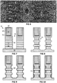
FIG 7 to FIG 13 schematically depict semiconductor structures at different stages of an illustrative process flow in accordance with exemplary embodiments of the present invention. - In the different figures, the same reference signs refer to the same or analogous elements.
- The present invention will be described with respect to particular embodiments and with reference to certain drawings but the invention is not limited thereto but only by the claims. The drawings described are only schematic and are non-limiting. In the drawings, the size of some of the elements may be exaggerated and not drawn on scale for illustrative purposes. The dimensions and the relative dimensions do not correspond to actual reductions to practice of the invention.
- Furthermore, the terms first, second, third and the like in the description and in the claims, are used for distinguishing between similar elements and not necessarily for describing a sequence, either temporally, spatially, in ranking or in any other manner. It is to be understood that the terms so used are interchangeable under appropriate circumstances and that the embodiments of the invention described herein are capable of operation in other sequences than described or illustrated herein.
- Moreover, the terms top, bottom, over, under and the like in the description and the claims are used for descriptive purposes and not necessarily for describing relative positions. It is to be understood that the terms so used are interchangeable with their antonyms under appropriate circumstances and that the embodiments of the invention described herein are capable of operation in other orientations than described or illustrated herein.
- It is to be noticed that the term "comprising", used in the claims, should not be interpreted as being restricted to the means listed thereafter; it does not exclude other elements or steps. It is thus to be interpreted as specifying the presence of the stated features, integers, steps or components as referred to, but does not preclude the presence or addition of one or more other features, integers, steps or components, or groups thereof. The term "comprising" therefore covers the situation where only the stated features are present and the situation where these features and one or more other features are present. Thus, the scope of the expression "a device comprising means A and B" should not be interpreted as being limited to devices consisting only of components A and B. It means that with respect to the present invention, the only relevant components of the device are A and B.
- Reference throughout this specification to "one embodiment" or "an embodiment" means that a particular feature, structure or characteristic described in connection with the embodiment is included in at least one embodiment of the present invention. Thus, appearances of the phrases "in one embodiment" or "in an embodiment" in various places throughout this specification are not necessarily all referring to the same embodiment, but may. Furthermore, the particular features, structures or characteristics may be combined in any suitable manner, as would be apparent to one of ordinary skill in the art from this disclosure, in one or more embodiments.
- Similarly, it should be appreciated that in the description of exemplary embodiments of the invention, various features of the invention are sometimes grouped together in a single embodiment, figure, or description thereof for the purpose of streamlining the disclosure and aiding in the understanding of one or more of the various inventive aspects. This method of disclosure, however, is not to be interpreted as reflecting an intention that the claimed invention requires more features than are expressly recited in each claim. Rather, as the following claims reflect, inventive aspects lie in less than all features of a single foregoing disclosed embodiment. Thus, the claims following the detailed description are hereby expressly incorporated into this detailed description, with each claim standing on its own as a separate embodiment of this invention.
- Furthermore, while some embodiments described herein include some but not other features included in other embodiments, combinations of features of different embodiments are meant to be within the scope of the invention, and form different embodiments, as would be understood by those in the art. For example, in the following claims, any of the claimed embodiments can be used in any combination.
- In the description provided herein, numerous specific details are set forth. However, it is understood that embodiments of the invention may be practised without these specific details. In other instances, well-known methods, structures and techniques have not been shown in detail in order not to obscure an understanding of this description.
- Reference will be made to transistors. These are devices having a first main terminal (e.g. a source or collector), a second main terminal (e.g. a drain or emitter) and a control terminal (e.g. a gate or base) for controlling the flow of electrical charges between the first and second main terminals.
- The following terms are provided solely to aid in the understanding of the invention.
- As used herein, and unless otherwise specified, under 'source/drain structure' is understood a 'source structure and/or drain structure'. In embodiments, a source structure and a drain structure may be comparable (e.g. indistinguishable) and their designation may depend on a relative voltage difference that is put across them in the final semiconductor structure.
- As used herein, and unless otherwise specified, when a first entity (e.g. a first layer or material) is said to be removed (e.g. etched) selectively with respect to a second entity (e.g. a second layer or material), this means that the first entity is removed faster than the second entity. Preferably, the removal (e.g. etching) process would remove the first entity at least twice faster, or more preferably at least five times faster, yet more preferably at least ten times faster, than the second entity. In some preferred embodiments, the second entity may be substantially not removed by the removal process.
- As used herein, and unless otherwise specified, a 'dummy' entity (e.g. a dummy gate region) is a non-functional entity which is typically used as a placeholder, to be replaced by a functional entity at some later stage of the semiconductor processing. For example, a dummy gate region may be replaced by a functional gate region during a replacement metal gate process. The 'dummy' entity may alternatively be referred to as a 'sacrificial' entity.
- In a first aspect, the present invention relates to a method for forming a semiconductor structure, comprising: (a) providing a structure comprising (i) a substrate, (ii) a layer stack on the substrate, the layer stack comprising at least one semiconductor layer of a semiconductor material and at least one sacrificial layer under the semiconductor layer, and (iii) a trench through the layer stack; (b) forming a recess in the layer stack by etching a portion of the sacrificial layer exposed by the trench, the etching being such that the sacrificial layer is etched preferentially with respect to the semiconductor layer; and (c) epitaxially growing a liner of the semiconductor material onto surfaces of the semiconductor layer exposed by the trench.
- In embodiments, the semiconductor structure may comprise-or may be-a gate-all-around (GAA) field-effect transistor (FET), such as a nanowire, nanosheet, forksheet or complementary field-effect transistor. In embodiments, the method may thus be for forming a gate-all-around field-effect transistor, preferably a nanowire, nanosheet, forksheet or complementary field-effect transistor. Forksheet FETs have for example been described by Weckx et al. (WECKX, P., et al. Novel forksheet device architecture as ultimate logic scaling device towards 2nm. In: 2019 IEEE International Electron Devices Meeting (IEDM). IEEE, 2019. p. 36.5. 1-36.5. 4.), which is incorporated herein by reference.
- In embodiments, the substrate may be a semiconductor substrate, such as a group IV substrate (e.g. Si, Ge or SiGe), a III-V substrate or a semiconductor-on-insulator substrate.
- The at least one semiconductor layer is a layer of the semiconductor material; i.e. it may comprise or consist of the semiconductor material. In some embodiments, a bulk of the semiconductor layer may substantially comprise (e.g. consist of) the semiconductor material while a surface or interface comprises (e.g. consist of) a derivative of the semiconductor material (e.g. a native oxide or an intermixed material). In embodiments, the semiconductor material may be a group IV material (e.g. Si, Ge or SiGe) or a III-V material (e.g. AlxGa1-xAs, GaN, InAs or Gaxln1-xP). In embodiments, the semiconductor layer may be a nanowire or a nanosheet, preferably a nanosheet.
- The at least one sacrificial layer is typically a layer of a sacrificial material; i.e. it may comprise or consist of the sacrificial material. In embodiments, the sacrificial material may likewise be a semiconductor material (in which case it could alternatively be referred to as a 'sacrificial semiconductor material'). In embodiments, the sacrificial layer may be a nanowire or a nanosheet, preferably a nanosheet. The designation 'semiconductor layer/material' and 'sacrificial layer/material' thus refers to their function in the method. More in particular, a semiconductor layer is typically to be maintained through the method (e.g. in order to fulfil an active role in the final semiconductor structure), whereas a sacrificial layer is intended to be sacrificed in the course of the method. As such, the semiconductor layer/material could also be referred to as an 'active semiconductor layer/material' (e.g. in contrast with a 'sacrificial semiconductor layer/material'). The aforementioned notwithstanding, the sacrificial and semiconductor materials may-though need not-be selected from a same list of materials; for example, SiGe could be a sacrificial material in one embodiment and a semiconductor material in different embodiment.
- In embodiments, the layer stack may comprise a plurality of semiconductor layers alternated with sacrificial layers. In preferred embodiments, at least a bottom layer of the layer stack may be one of the sacrificial layers. In embodiments, a top layer of the layer stack may be one of semiconductor layers or one of the sacrificial layers.
- In embodiments, the semiconductor structure may further comprise: (vi) a dummy gate region over (e.g. directly on) the layer stack. In embodiments, the dummy gate region may comprise a dummy gate oxide (e.g. SiO2) and a dummy gate (e.g. poly-Si). In embodiments, the semiconductor structure may further comprise: (vii) gate spacers (e.g. SiCON or SiBCN) flanking the dummy gate region.
- Note that-even though the sacrificial layer is in step b etched preferentially with respect to the semiconductor layer-the etch selectivity that can be achieved is typically inevitably finite (i.e. a perfect selectivity cannot be achieved), so that some semiconductor material loss is typically unavoidable (cf. supra). As such, a portion of the semiconductor layer will nevertheless also be etched in step b.
- In view of this finite etch selectivity, step c then allows to (at least partially) recover this semiconductor material loss, by epitaxially growing the semiconductor material liner onto surfaces of the semiconductor layer exposed by the trench. In some embodiments, the liner may be grown epitaxially onto the semiconductor layer surfaces selectively with respect to surfaces of the sacrificial layer. In other embodiments, step c may further comprise growing the liner onto surfaces of the sacrificial layer exposed by the trench (i.e. the liner may be grown epitaxially onto both semiconductor layer surfaces and sacrificial layer surfaces). Having the liner also on the sacrificial layer surfaces may have an undesired effect in that also this portion of the liner will typically remain in the final semiconductor structure and can increase the parasitic capacitance therein (e.g. by reducing the effectiveness of the inner spacers; cf. infra). As such,-where possible-it may be preferred to selectively grow the liner only on the semiconductor layer surfaces. However, for some combinations of semiconductor and sacrificial layers (e.g. Si and SiGe), such growth selectivity may be challenging or even impossible to achieve. Nevertheless, growing the liner on both the semiconductor layer surfaces and sacrificial layer surfaces still yields beneficial results, though it may be desired to then take into account the effect of the liner on e.g. the parasitic capacitance in the final semiconductor structure. For example, this may comprise striking a balance between a good access resistance and a good parasitic capacitance through an appropriate selection of the liner thickness; i.e. thick enough to sufficiently increase the access resistance (e.g. through a larger contact area with the source/drain structure) but also thin enough to excessively increase the parasitic capacitance.
- In embodiments, the liner grown in step c may have a thickness of 3 nm or less, preferably 2.5 nm or less, more preferably 2 nm or less, yet more preferably 1.5 nm or less, such as 1.2 nm or less. In embodiments, the liner grown in step c may have a thickness of at least 0.5 nm, yet more preferably at least 1 nm. The thickness of the liner may advantageously be selected in order to-at least partially-compensate the semiconductor material loss in step b, but may also take into account other factors such as its influence on the parasitic capacitance (cf. supra). To that effect, the liner thickness (t2 in
FIG 5 ) could be equal to (i.e. fully compensating the semiconductor layer's distal thickness thinning) the semiconductor material loss (t1 inFIG 4 ), or it may be smaller (i.e. partially compensating) or larger (i.e. overcompensating). - In embodiments, the method may comprise a further step d-after step c-, of: (d) filling the recess with a dielectric material, thereby forming an inner spacer (which may alternatively be referred to as an 'internal spacer'). The inner spacer is typically advantageously used to reduce the parasitic capacitance in the final semiconductor structure (e.g. between a gate region and a source/drain structure; cf. infra).
- In embodiments, the method may comprise a further step e-after step d-, of: (e) forming a source/drain structure (e.g. SiGe:B or Si:P) in the trench. In embodiments, forming the source/drain structure in the trench may comprise epitaxially growing the source/drain structure in the trench. The source/drain structure (e.g. source/drain contact) is typically advantageously used to make contact with source/drain regions of the semiconductor layers the final semiconductor structure.
- In embodiments, the method may comprise a further step f of: (f) removing the sacrificial layer. In embodiments, step f may be performed after step d, preferably after step e. In embodiments, removing the sacrificial layer may be performed preferentially (e.g. selectively) with respect to the semiconductor layer and liner, preferably preferentially with respect to the semiconductor layer, liner and inner spacer. For example, removing the sacrificial layer may be performed preferentially with respect to the semiconductor layer, liner, inner spacer and source/drain structure. An opening is typically obtained where the sacrificial layer was removed. The aforementioned notwithstanding, as before a perfect selectivity for removing the sacrificial layer with respect to the semiconductor layer and liner can typically not be achieved, so that some semiconductor material (of the semiconductor layer and/or liner) will normally nevertheless be removed as well during step f. For example,-where the liner makes contact with the sacrificial layer-up to about 1 nm of liner thickness could be lost during step f. For these regions of the liner, the thickness of the liner may after step f be 2 nm or less, preferably 1.5 nm or less, more preferably 1.2 nm or, yet more preferably 1 nm or less, most preferably 0.8 nm or less, such as being completely removed. (Partially) removing the liner where it contacts the sacrificial layer may be advantageous as it is typically these portions of the liner which also most negatively impact the parasitic capacitance, while at the same time contributing less to the improvement in access resistance.
- In embodiments, step f may further comprise removing the dummy gate region (e.g. prior to or concurrently with removing the sacrificial layer). Step f may also be referred to as a semiconductor layer release step (e.g. a nanowire or nanosheet release).
- In embodiments, the method may comprise a further step g-after step f-of: (g) forming a gate region (e.g. a functional gate region) where the sacrificial layer was removed in step f. Step g may thus comprise forming a gate region in the opening obtained after step f. In embodiments, forming the gate region may comprise forming a gate dielectric (e.g. a high-k dielectric, such as HfO2), a work function metal (e.g. TiN, TiAl or TaN) and a gate metal (e.g. W, Co or Ru). In embodiments, the gate region may be a gate-all-around gate region. A replacement metal gate (RMG) process may for example be used to perform steps f and g.
- In embodiments, any feature of any embodiment of the first aspect may independently be as correspondingly described for any embodiment of any of the other aspects.
- In a second aspect, the present invention relates to a semiconductor structure, comprising: (i) a substrate; (ii) a layer stack on the substrate, the layer stack comprising at least one semiconductor layer of a semiconductor material and at least one ancillary layer under the semiconductor layer; (iii) a trench through the layer stack; (iv) a recess with respect to the semiconductor layer, the recess abutting the ancillary layer; and (v) a liner of the semiconductor material lining the semiconductor layer-and optionally the ancillary layer-with respect to the trench.
- Embodiments of the second aspect thus correspond to the semiconductor structure obtainable after any of steps c-g.
- In embodiments, the semiconductor structure may further comprise: (vi) a dummy gate region over (e.g. directly on) the layer stack. In embodiments, the dummy gate region may comprise a dummy gate oxide (e.g. SiO2) and a dummy gate (e.g. poly-Si). In embodiments, the semiconductor structure may further comprise: (vii) gate spacers (e.g. SiCON or SiBCN) flanking the dummy gate region.
- In embodiments, the ancillary layer may comprise a sacrificial layer, an opening or a gate region.
- In embodiments, the recess may comprise an inner spacer.
- In embodiments, the trench may comprise a source/drain structure.
- In embodiments, any feature of any embodiment of the second aspect may independently be as correspondingly described for any embodiment of any of the other aspects.
- In a third aspect, the present invention relates to a use of a liner of semiconductor material in a semiconductor structure as defined in any of embodiment of the second aspect, for decreasing an access resistance to the semiconductor layer.
- In embodiments, any feature of any embodiment of the third aspect may independently be as correspondingly described for any embodiment of any of the other aspects.
- The invention will now be described by a detailed description of several embodiments of the invention. It is clear that other embodiments of the invention can be configured according to the knowledge of the person skilled in the art without departing from the true technical teaching of the invention, the invention being limited only by the terms of the appended claims.
- As an example of embodiments of the present invention, an illustrative process flow for forming a gate-all-around field-effect transistor (e.g. a nanowire, nanosheet, forksheet or complementary field-effect transistor) is depicted in
FIG 7 to FIG 13 and described herebelow. - We now refer to
FIG 7 . A semiconductor structure (10) was provided, comprising a layer stack (30) of alternating sacrificial layers (32) (e.g. SiGe, such as SiGe nanowires or nanosheets) and semiconductor layers (31) (e.g. Si, such as Si nanowires or nanosheets) on a substrate (20) (e.g. a Si wafer). The semiconductor structure (10) further comprised one or more trenches (40), through the layer stack (30) down to the substrate (20); one or more dummy gate regions (50) over the layer stack (30) (e.g. a SiO2 dummy gate oxide (51) and a poly-Si dummy gate (52)); and gate spacers (e.g. SiCON or SiBCN) (60) flanking the dummy gate region (50). - We now refer to
FIG 8 . One or more recesses (70) were formed in the layer stack (30) by etching a portion of the sacrificial layer (32) exposed by the trench (40). The sacrificial layers (32) were etched preferentially with respect to the semiconductor layer (31), but the selectivity was inevitably imperfect (cf. supra) so that some semiconductor material loss (and possibly substrate (20) material loss) necessarily also occurs (cf.FIG 3, FIG 4 andFIG 6 ). - We now refer to
FIG 9 . In order to compensate the semiconductor material loss, a liner (80) of the semiconductor material (e.g. Si) was epitaxially grown onto surfaces of the semiconductor layers (31)-and optionally of the sacrificial layers (32) and/or substrate (20)-exposed by the trench (40). For example, the liner (80) could line an entire bottom portion of trench (40) extending up to the gate spacers (60). Depending on the desired outcome, the liner (80) could have a thickness (t2 inFIG 5 ) smaller than, equal to or larger than the semiconductor material loss (t1 inFIG 4 ); i.e. the thinning of the distal thickness (d) may be respectively partially, fully (cf.FIG 5 ) or overcompensated. For example, where the liner (80) lines both the semiconductor layers (31) and the sacrificial layers (32), a thicker liner (80) will typically lead to a lower access resistance to the semiconductor layers (31) but will also result in a higher parasitic capacitance. A balance between both may thus be sought by selecting an appropriate thickness (t2) for the liner (80). - We now refer to
FIG 10 . The recesses (70) were filled with a dielectric material, thereby forming inner spacers (71). - We now refer to
FIG 11 . The trench (40) was filled (e.g. by epitaxial growth of SiGe:B or Si:P) to form a source/drain structure (41). - We now refer to
FIG 12 . The semiconductor layers (31) are released by removing the dummy gate regions (50) and sacrificial layers (32). - We now refer to
FIG 13 . Functional replacement gate regions comprising a gate dielectric (e.g. HfO2), work function metal stack (e.g. TiN, TiAl or TaN), and metal gate fill (e.g. W, Co or Ru) (91) were formed in the openings (90) where the sacrificial layers (32) and dummy gate regions (50) were previously removed. - It is to be understood that although preferred embodiments, specific constructions and configurations, as well as materials, have been discussed herein for devices according to the present invention, various changes or modifications in form and detail may be made without departing from the scope and technical teachings of this invention. For example, any formulas given above are merely representative of procedures that may be used. Functionality may be added or deleted from the block diagrams and operations may be interchanged among functional blocks. Steps may be added or deleted to methods described within the scope of the present invention.
Claims (15)
- A method for forming a semiconductor structure (10), comprising:a. providing a structure comprisingi. a substrate (20),ii. a layer stack (30) on the substrate (20), the layer stack (30) comprising at least one semiconductor layer (31) of a semiconductor material and at least one sacrificial layer (32) under the semiconductor layer (31), andiii. a trench (40) through the layer stack (30);b. forming a recess (70) in the layer stack (30) by etching a portion of the sacrificial layer (32) exposed by the trench (40), the etching being such that the sacrificial layer (32) is etched preferentially with respect to the semiconductor layer (31); andc. epitaxially growing a liner (80) of the semiconductor material onto surfaces of the semiconductor layer (31) exposed by the trench (40).
- The method according to claim 1, wherein step c further comprises growing the liner (80) onto surfaces of the sacrificial layer exposed by the trench (40).
- The method according to any of the previous claims, wherein the liner (80) grown in step c has a thickness (t2) of 3 nm or less, preferably 2.5 nm or less, more preferably 2 nm or less, yet more preferably 1.5 nm or less.
- The method according to any of the previous claims, wherein the layer stack (30) comprises a plurality of semiconductor layers (31) alternated with sacrificial layers (32).
- The method according to any of the previous claims, wherein the semiconductor material is a group IV or III-V material.
- The method according to claim 5, comprising a further step d-after step c-, of:
d. filling the recess (70) with a dielectric material, thereby forming an inner spacer. - The method according to claim 6, comprising a further step e-after step d-, of:
e. forming a source/drain structure (41) in the trench (40). - The method according to any of the previous claims, comprising a further step f of:
f. removing the sacrificial layer (32). - The method according to claim 8, comprising a further step g-after step f-of:
g. forming a gate region (91) where the sacrificial layer (32) was removed in step f. - The method according to any of the previous claims, for forming a gate-all-around field-effect transistor, preferably a nanowire, nanosheet, forksheet or complementary field-effect transistor.
- A semiconductor structure (10), comprising:i. a substrate (20);ii. a layer stack (30) on the substrate (20), the layer stack (30) comprising at least one semiconductor layer (31) of a semiconductor material and at least one ancillary layer under the semiconductor layer (31);iii. a trench (40) through the layer stack (30);iv. a recess (70) with respect to the semiconductor layer (31), the recess (70) abutting the ancillary layer; andv. a liner (80) of the semiconductor material lining the semiconductor layer (31)-and optionally the ancillary layer-with respect to the trench (40).
- The semiconductor structure (10) according to claims 11, wherein the recess (70) comprises an inner spacer.
- The semiconductor structure (10) according to any of claims 11 to 12, wherein the trench (40) comprises a source/drain structure (41).
- The semiconductor structure (10) according to any of claims 11 to 13, wherein the ancillary layer comprises a sacrificial layer (32), an opening (90) or a gate region (91).
- Use of a liner (80) of semiconductor material in a semiconductor structure (10) as defined in any of claims 11 to 14, for decreasing an access resistance to the semiconductor layer (31).
Priority Applications (3)
| Application Number | Priority Date | Filing Date | Title |
|---|---|---|---|
| EP20173771.5A EP3907179A1 (en) | 2020-05-08 | 2020-05-08 | Counteracting semiconductor material loss during semiconductor structure formation |
| US17/308,453 US11996459B2 (en) | 2020-05-08 | 2021-05-05 | Counteracting semiconductor material loss during semiconductor structure formation |
| CN202110501404.9A CN113628966A (en) | 2020-05-08 | 2021-05-08 | Counteracting semiconductor material loss during semiconductor structure formation |
Applications Claiming Priority (1)
| Application Number | Priority Date | Filing Date | Title |
|---|---|---|---|
| EP20173771.5A EP3907179A1 (en) | 2020-05-08 | 2020-05-08 | Counteracting semiconductor material loss during semiconductor structure formation |
Publications (1)
| Publication Number | Publication Date |
|---|---|
| EP3907179A1 true EP3907179A1 (en) | 2021-11-10 |
Family
ID=70681637
Family Applications (1)
| Application Number | Title | Priority Date | Filing Date |
|---|---|---|---|
| EP20173771.5A Withdrawn EP3907179A1 (en) | 2020-05-08 | 2020-05-08 | Counteracting semiconductor material loss during semiconductor structure formation |
Country Status (3)
| Country | Link |
|---|---|
| US (1) | US11996459B2 (en) |
| EP (1) | EP3907179A1 (en) |
| CN (1) | CN113628966A (en) |
Cited By (1)
| Publication number | Priority date | Publication date | Assignee | Title |
|---|---|---|---|---|
| EP4598305A3 (en) * | 2024-02-05 | 2025-09-24 | Samsung Electronics Co., Ltd. | Semiconductor device including different inner spacers |
Families Citing this family (2)
| Publication number | Priority date | Publication date | Assignee | Title |
|---|---|---|---|---|
| US11610977B2 (en) * | 2020-07-28 | 2023-03-21 | Taiwan Semiconductor Manufacturing Co., Ltd. | Methods of forming nano-sheet-based devices having inner spacer structures with different widths |
| US11444178B2 (en) | 2020-11-13 | 2022-09-13 | Taiwan Semiconductor Manufacturing Company, Ltd. | Inner spacer liner |
Citations (3)
| Publication number | Priority date | Publication date | Assignee | Title |
|---|---|---|---|---|
| US20180294331A1 (en) * | 2017-04-05 | 2018-10-11 | Samsung Electronics Co., Ltd. | Semiconductor device |
| US20190058052A1 (en) * | 2017-08-18 | 2019-02-21 | Globalfoundries Inc. | Inner spacer formation in a nanosheet field-effect transistor |
| US20190341467A1 (en) * | 2017-12-19 | 2019-11-07 | International Business Machines Corporation | Nanosheet device with close source drain proximity |
Family Cites Families (10)
| Publication number | Priority date | Publication date | Assignee | Title |
|---|---|---|---|---|
| US9647139B2 (en) * | 2015-09-04 | 2017-05-09 | International Business Machines Corporation | Atomic layer deposition sealing integration for nanosheet complementary metal oxide semiconductor with replacement spacer |
| US10269983B2 (en) | 2017-05-09 | 2019-04-23 | Globalfoundries Inc. | Stacked nanosheet field-effect transistor with air gap spacers |
| US9954058B1 (en) | 2017-06-12 | 2018-04-24 | International Business Machines Corporation | Self-aligned air gap spacer for nanosheet CMOS devices |
| US9947804B1 (en) | 2017-07-24 | 2018-04-17 | Globalfoundries Inc. | Methods of forming nanosheet transistor with dielectric isolation of source-drain regions and related structure |
| US10535733B2 (en) | 2018-01-11 | 2020-01-14 | International Business Machines Corporation | Method of forming a nanosheet transistor |
| US10720494B2 (en) * | 2018-01-22 | 2020-07-21 | Globalfoundries Inc. | Field-effect transistors with airgaps |
| US10566438B2 (en) | 2018-04-02 | 2020-02-18 | International Business Machines Corporation | Nanosheet transistor with dual inner airgap spacers |
| US10615256B2 (en) * | 2018-06-27 | 2020-04-07 | International Business Machines Corporation | Nanosheet transistor gate structure having reduced parasitic capacitance |
| US11043578B2 (en) * | 2018-08-30 | 2021-06-22 | Taiwan Semiconductor Manufacturing Co., Ltd. | Nanowire stack GAA device with inner spacer |
| US11444202B2 (en) * | 2020-01-17 | 2022-09-13 | Taiwan Semiconductor Manufacturing Company, Ltd. | Semiconductor device and method of forming the same |
-
2020
- 2020-05-08 EP EP20173771.5A patent/EP3907179A1/en not_active Withdrawn
-
2021
- 2021-05-05 US US17/308,453 patent/US11996459B2/en active Active
- 2021-05-08 CN CN202110501404.9A patent/CN113628966A/en active Pending
Patent Citations (3)
| Publication number | Priority date | Publication date | Assignee | Title |
|---|---|---|---|---|
| US20180294331A1 (en) * | 2017-04-05 | 2018-10-11 | Samsung Electronics Co., Ltd. | Semiconductor device |
| US20190058052A1 (en) * | 2017-08-18 | 2019-02-21 | Globalfoundries Inc. | Inner spacer formation in a nanosheet field-effect transistor |
| US20190341467A1 (en) * | 2017-12-19 | 2019-11-07 | International Business Machines Corporation | Nanosheet device with close source drain proximity |
Non-Patent Citations (3)
Cited By (1)
| Publication number | Priority date | Publication date | Assignee | Title |
|---|---|---|---|---|
| EP4598305A3 (en) * | 2024-02-05 | 2025-09-24 | Samsung Electronics Co., Ltd. | Semiconductor device including different inner spacers |
Also Published As
| Publication number | Publication date |
|---|---|
| US11996459B2 (en) | 2024-05-28 |
| US20210351275A1 (en) | 2021-11-11 |
| CN113628966A (en) | 2021-11-09 |
Similar Documents
| Publication | Publication Date | Title |
|---|---|---|
| US11996459B2 (en) | Counteracting semiconductor material loss during semiconductor structure formation | |
| US10854752B2 (en) | High mobility strained channels for fin-based NMOS transistors | |
| TWI438867B (en) | CMOS device with different types and thicknesses of gate insulating layer and forming method thereof | |
| US9935198B2 (en) | Method for inducing strain in vertical semiconductor columns | |
| US6939751B2 (en) | Method and manufacture of thin silicon on insulator (SOI) with recessed channel | |
| US20090001415A1 (en) | Multi-gate transistor with strained body | |
| US10504916B2 (en) | Semiconductor device and method of manufacturing the same | |
| JP2018026565A (en) | Extension region for semiconductor device | |
| JP6315948B2 (en) | FinFET having dual strain channel and method of manufacturing the same | |
| TW201212244A (en) | Methods for manufacturing bulk silicon and SOI CMOS devices by gate stress engineering with SiGe and/or Si:C | |
| US9917020B2 (en) | Methods for fabricating an integrated circuit having vertically overlapping short and long channel FinFETs | |
| TW201015663A (en) | Method for fabricating a semiconductor device | |
| US20250107172A1 (en) | Multi-stack semiconductor device with zebra nanosheet structure | |
| US20190081156A1 (en) | Method for Forming a Vertical Channel Device, and a Vertical Channel Device | |
| CN101689508A (en) | Method for forming dual metal gate structure | |
| JP2009545173A (en) | Raised STI structure and super damascene technology to increase NMOSFET performance using embedded silicon carbon | |
| US6395589B1 (en) | Fabrication of fully depleted field effect transistor with high-K gate dielectric in SOI technology | |
| CN117790315A (en) | Preparation method of gird transistor containing pn junction isolation structure | |
| EP1638149A2 (en) | Method of manufacture of an heterostructure channel insulated gate field effect transistor and corresponding transistor | |
| EP3185299A1 (en) | Self-alligned nanostructures for semi-conductor device | |
| US11088263B2 (en) | Method of forming vertical field effect transistor device | |
| US8779525B2 (en) | Method for growing strain-inducing materials in CMOS circuits in a gate first flow | |
| CN1988116B (en) | Method of manufacturing a field effect transistor and transistor structure manufactured thereby | |
| US20210074830A1 (en) | Isolated Vertical Nanowire | |
| US7081392B2 (en) | Method for fabricating a gate structure of a FET and gate structure of a FET |
Legal Events
| Date | Code | Title | Description |
|---|---|---|---|
| PUAI | Public reference made under article 153(3) epc to a published international application that has entered the european phase |
Free format text: ORIGINAL CODE: 0009012 |
|
| STAA | Information on the status of an ep patent application or granted ep patent |
Free format text: STATUS: THE APPLICATION HAS BEEN PUBLISHED |
|
| AK | Designated contracting states |
Kind code of ref document: A1 Designated state(s): AL AT BE BG CH CY CZ DE DK EE ES FI FR GB GR HR HU IE IS IT LI LT LU LV MC MK MT NL NO PL PT RO RS SE SI SK SM TR |
|
| B565 | Issuance of search results under rule 164(2) epc |
Effective date: 20201015 |
|
| STAA | Information on the status of an ep patent application or granted ep patent |
Free format text: STATUS: THE APPLICATION IS DEEMED TO BE WITHDRAWN |
|
| 18D | Application deemed to be withdrawn |
Effective date: 20220511 |