EP3907083A1 - Repair chip, ink cartridge, and printer - Google Patents
Repair chip, ink cartridge, and printer Download PDFInfo
- Publication number
- EP3907083A1 EP3907083A1 EP20899508.4A EP20899508A EP3907083A1 EP 3907083 A1 EP3907083 A1 EP 3907083A1 EP 20899508 A EP20899508 A EP 20899508A EP 3907083 A1 EP3907083 A1 EP 3907083A1
- Authority
- EP
- European Patent Office
- Prior art keywords
- point
- chip
- repair
- tin
- ink cartridge
- Prior art date
- Legal status (The legal status is an assumption and is not a legal conclusion. Google has not performed a legal analysis and makes no representation as to the accuracy of the status listed.)
- Granted
Links
Images


Classifications
-
- B—PERFORMING OPERATIONS; TRANSPORTING
- B41—PRINTING; LINING MACHINES; TYPEWRITERS; STAMPS
- B41J—TYPEWRITERS; SELECTIVE PRINTING MECHANISMS, i.e. MECHANISMS PRINTING OTHERWISE THAN FROM A FORME; CORRECTION OF TYPOGRAPHICAL ERRORS
- B41J2/00—Typewriters or selective printing mechanisms characterised by the printing or marking process for which they are designed
- B41J2/005—Typewriters or selective printing mechanisms characterised by the printing or marking process for which they are designed characterised by bringing liquid or particles selectively into contact with a printing material
- B41J2/01—Ink jet
- B41J2/17—Ink jet characterised by ink handling
- B41J2/175—Ink supply systems ; Circuit parts therefor
- B41J2/17503—Ink cartridges
- B41J2/17526—Electrical contacts to the cartridge
- B41J2/1753—Details of contacts on the cartridge, e.g. protection of contacts
-
- B—PERFORMING OPERATIONS; TRANSPORTING
- B41—PRINTING; LINING MACHINES; TYPEWRITERS; STAMPS
- B41J—TYPEWRITERS; SELECTIVE PRINTING MECHANISMS, i.e. MECHANISMS PRINTING OTHERWISE THAN FROM A FORME; CORRECTION OF TYPOGRAPHICAL ERRORS
- B41J2/00—Typewriters or selective printing mechanisms characterised by the printing or marking process for which they are designed
- B41J2/005—Typewriters or selective printing mechanisms characterised by the printing or marking process for which they are designed characterised by bringing liquid or particles selectively into contact with a printing material
- B41J2/01—Ink jet
- B41J2/17—Ink jet characterised by ink handling
- B41J2/175—Ink supply systems ; Circuit parts therefor
- B41J2/17503—Ink cartridges
- B41J2/17543—Cartridge presence detection or type identification
- B41J2/17546—Cartridge presence detection or type identification electronically
-
- B—PERFORMING OPERATIONS; TRANSPORTING
- B41—PRINTING; LINING MACHINES; TYPEWRITERS; STAMPS
- B41J—TYPEWRITERS; SELECTIVE PRINTING MECHANISMS, i.e. MECHANISMS PRINTING OTHERWISE THAN FROM A FORME; CORRECTION OF TYPOGRAPHICAL ERRORS
- B41J2/00—Typewriters or selective printing mechanisms characterised by the printing or marking process for which they are designed
- B41J2/005—Typewriters or selective printing mechanisms characterised by the printing or marking process for which they are designed characterised by bringing liquid or particles selectively into contact with a printing material
- B41J2/01—Ink jet
- B41J2/17—Ink jet characterised by ink handling
- B41J2/175—Ink supply systems ; Circuit parts therefor
- B41J2/17503—Ink cartridges
- B41J2/17553—Outer structure
-
- B—PERFORMING OPERATIONS; TRANSPORTING
- B41—PRINTING; LINING MACHINES; TYPEWRITERS; STAMPS
- B41J—TYPEWRITERS; SELECTIVE PRINTING MECHANISMS, i.e. MECHANISMS PRINTING OTHERWISE THAN FROM A FORME; CORRECTION OF TYPOGRAPHICAL ERRORS
- B41J2/00—Typewriters or selective printing mechanisms characterised by the printing or marking process for which they are designed
- B41J2/005—Typewriters or selective printing mechanisms characterised by the printing or marking process for which they are designed characterised by bringing liquid or particles selectively into contact with a printing material
- B41J2/01—Ink jet
- B41J2/17—Ink jet characterised by ink handling
- B41J2/175—Ink supply systems ; Circuit parts therefor
- B41J2/17503—Ink cartridges
- B41J2/17559—Cartridge manufacturing
Definitions
- connection can be a fixed connection, a detachable connection, or an integrated connection. It can also be a mechanical connection or an electrical connection. It can be a direct connection or an indirect connection through an intermediary. It can be an internal connection of two components.
- connection can be a fixed connection, a detachable connection, or an integrated connection. It can also be a mechanical connection or an electrical connection. It can be a direct connection or an indirect connection through an intermediary. It can be an internal connection of two components.
- the specific meaning of the above terms in the present disclosure may be understood on a case-by-case basis by the skilled in the art.
Landscapes
- Engineering & Computer Science (AREA)
- Manufacturing & Machinery (AREA)
- Ink Jet (AREA)
Abstract
Description
- This application claims all benefits of the priority from
China Patent Application No. 201922234380.6, filed on December 13, 2019 - The present disclosure generally relates to a technical field of a printing device, and in particular, to a repair chip, an ink cartridge, and a printer.
- An ink cartridge is a member of an inkjet printer, which is used to store ink for printing and then complete the printing. The ink cartridge can be an integrated ink cartridge with a head or a splitting ink cartridge. The integrated ink cartridge integrates a nozzle on the cartridge. When the ink runs out and the integrated ink cartridge needs to be replaced, the nozzle will be replaced accordingly. Therefore, high printing accuracy and printing quality can be achieved, but the cost of the integrated ink cartridge is relatively high. In order to reduce the cost of the integrated ink cartridge, a used ink cartridge can be recycled and reused. In generally, a recycled ink cartridge is usually an old ink cartridge that cannot be used immediately due to damage of a resistance of a chip on the ink cartridge. As a result, the ink cartridge is often scrapped and cannot be used again.
- There is no effective solution yet to solve this problem of low utilization rate of the recycled ink cartridge.
- According to embodiments of the present disclosure, a repair chip is provided, which can be applied to an ink cartridge. The repair chip includes a substrate, a first contact point, a second contact point, a first tin point, a second tin point and a repair resistor. The substrate has a first surface and a second surface opposite to each other. The first contact point and the second contact point are located on the first surface. The first tin point, the second tin point and the repair resistor are located on the second surface. The first tin point is corresponding to the first contact point, and the second tin point is corresponding to the second contact point. The first tin point is connected with a first end of the repair resistor, and the second tin point is connected with a second end of the repair resistor. The first contact point and the second contact point are configured for electrically connecting with a printer, respectively. The first contact point is connected with the first tin point, and the second contact point is connected with the second tin point. The first tin point and the second tin point are configured to connect with chip contact points of a chip of the ink cartridge, respectively. The second surface is bonded to a surface of the chip of the ink cartridge.
- In an embodiment of the present disclosure, the chip contact points of the chip include a contact point to be repaired and a grounding contact point. The first tin point is connected with the contact point to be repaired, and the second tin point is connected with the grounding contact point.
- In an embodiment of the present disclosure, the repair resistor is embedded in a first groove disposed on the ink cartridge.
- In an embodiment of the present disclosure, a thickness of the repair resistor matches a depth of the first groove.
- In an embodiment of the present disclosure, the second surface is further provided with a chip crystal, and the chip crystal is embedded in a second groove disposed on the ink cartridge.
- In an embodiment of the present disclosure, the repair resistor is embedded in a first groove disposed on the ink cartridge, and the second groove and the first groove are the same one.
- In an embodiment of the present disclosure, the first contact point is connected with the first tin point via a through hole filled with a conductor, and the second contact point is connected with the second tin point via a through hole filled with a conductor.
- In an embodiment of the present disclosure, the repair chip is provided with a locating portion. The locating portion includes a hole structure or a groove structure. The locating portion is configured to preposition the substrate when mounting the repair chip. The ink cartridge is provided with a positioning seat, and the locating portion coincides with a center of the positioning seat.
- In an embodiment of the present disclosure, the substrate is a flexible substrate.
- According to embodiments of the present disclosure, an ink cartridge is further provided. The ink cartridge includes an ink cartridge body, a chip of the ink cartridge and a repair chip. The repair chip includes a substrate, a first contact point, a second contact point, a first tin point, a second tin point and a repair resistor. The substrate has a first surface and a second surface opposite to each other. The first contact point and the second contact point are located on the first surface. The first tin point, the second tin point and the repair resistor are located on the second surface. The first tin point is corresponding to the first contact point, and the second tin point is corresponding to the second contact point. The first tin point is connected with a first end of the repair resistor, and the second tin point is connected with a second end of the repair resistor. The first contact point and the second contact point are configured for electrically connecting with a printer, respectively. The first contact point is connected with the first tin point, and the second contact point is connected with the second tin point. The ink cartridge body is connected with the chip of the ink cartridge. The first tin point and the second tin point are configured to connect with chip contact points of a chip of the ink cartridge, respectively. The second surface is bonded to a surface of the chip of the ink cartridge.
- In an embodiment of the present disclosure, the chip contact points of the chip of the ink cartridge include a contact point to be repaired and a grounding contact point. The first tin point is connected with the contact point to be repaired, and the second tin point is connected with the grounding contact point.
- In an embodiment of the present disclosure, the ink cartridge is provided with a first groove, and the repair resistor is embedded in the first groove.
- According to embodiments of the present disclosure, a printer is further provided. The printer includes a printer body, an ink cartridge body, a chip of the ink cartridge and a repair chip. The repair chip includes a substrate, a first contact point, a second contact point, a first tin point, a second tin point and a repair resistor. The substrate has a first surface and a second surface opposite to each other. The first contact point and the second contact point are located on the first surface. The first tin point, the second tin point and the repair resistor are located on the second surface. The first tin point is corresponding to the first contact point, and the second tin point is corresponding to the second contact point. The first tin point is connected with a first end of the repair resistor, and the second tin point is connected with a second end of the repair resistor. The first contact point and the second contact point are configured for electrically connecting with the printer body, respectively. The first contact point is connected with the first tin point, and the second contact point is connected with the second tin point. The ink cartridge body is connected with the chip of the ink cartridge. The first tin point and the second tin point are configured to connect with chip contact points of the chip of the ink cartridge, respectively. The second surface is bonded to a surface of the chip of the ink cartridge.
- The above repair chip, ink cartridge and printer have the following advantages: the repair resistor is located on the repair chip, the contact points are located on the first surface of the substrate, the tin points corresponding to the contact points are located on the second surface of the substrate, the repair resistor is connected with the tin points, and the tin points are connected with the chip contact points of the chip of the ink cartridge. As a result, a damaged resistor of the chip of the ink cartridge can be repaired, the recycled ink cartridge can be used normally after filling ink, and the utilization rate of the recycled ink cartridge is improved.
- To describe and illustrate embodiments and/or examples of the present disclosure made public here better, reference may be made to one or more of the figures. The additional details or examples used to describe the figures should not be construed as limiting the scope of any of the present disclosure, the embodiments and/or examples currently described, and the best model of the present disclosure as currently understood.
-
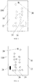
Fig. 1 is a schematic diagram of a first surface of a repair chip in an embodiment of the present disclosure. -
Fig. 2 is a schematic diagram of a second surface of a repair chip in an embodiment of the present disclosure. -
Fig. 3 is a schematic diagram of a first surface of another repair chip in another embodiment of the present disclosure. -
Fig. 4 is a schematic diagram of a second surface of another repair chip in another embodiment of the present disclosure. -
Fig. 5 is a schematic diagram of an ink cartridge in another embodiment of the present disclosure. -
Fig. 6 is a block diagram of a printer in another embodiment of the present disclosure. - In the figures, 100 represents a repair chip, 10 represents a substrate, 12 represents a first surface, 22 represents a second surface, 14 represents a first contact point, 16 represents a second contact point, 24 represents a first tin point, 26 represents a second tin point, 28 represents a repair resistor, 30 represents a locating portion, 40 represents a chip crystal, 110 represents an ink cartridge body, 120 represents a chip of an ink cartridge, 52 represents a first groove, and 62 represents a printer body.
- The technical solutions in the embodiments of the present disclosure are clearly and completely described in the following with reference to the accompanying drawings in the embodiments of the present disclosure. It is obvious that the described embodiments are only a part of the embodiments, but not all of the embodiments. All other embodiments obtained by those skilled in the art based on the embodiments of the present disclosure without departing from the inventive scope are the scope of the present disclosure.
- It should be understood that in the description of the present disclosure, an orientation or a position relationship indicated by location words such as "center, up, down, left, right, vertical, horizontal, inside and outside" are based on an orientation or a position relationship shown in the attached figures, which is only for the convenience of describing the present disclosure and simplifying the description. These location words do not indicate and imply that the device or element referred to must have a specific orientation or be constructed and operated in a specific orientation, so it cannot be understood as a restriction on the scope of the present disclosure. Furthermore, the terms "first", "second" and "third" are used only for descriptive purposes and cannot be understood to indicate or imply relative importance.
- In the description of the present disclosure, it should be noted that unless otherwise expressly stated and qualified, the terms "disposed", "joined" and "connected" are to be understood broadly. For example, the connection can be a fixed connection, a detachable connection, or an integrated connection. It can also be a mechanical connection or an electrical connection. It can be a direct connection or an indirect connection through an intermediary. It can be an internal connection of two components. The specific meaning of the above terms in the present disclosure may be understood on a case-by-case basis by the skilled in the art.
- Unless otherwise defined, all technical and scientific terms used herein have the same meaning as a skilled person in the art would understand. The terminology used in the description of the present disclosure is for the purpose of describing particular embodiments and is not intended to limit the present disclosure.
- In an embodiment, a repair chip applied to an ink cartridge is provided.
Fig. 1 is a schematic diagram of a first surface of a repair chip in an embodiment of the present disclosure.Fig. 2 is a schematic diagram of a second surface of a repair chip in an embodiment of the present disclosure. As shown inFig. 1 and Fig. 2 , therepair chip 100 includes asubstrate 10, afirst contact point 14, asecond contact point 16, afirst tin point 24, asecond tin point 26 and arepair resistor 28. Thesubstrate 10 has afirst surface 12 and asecond surface 22 opposite to each other. Thefirst contact point 14 and thesecond contact point 16 are located on thefirst surface 12. Thefirst contact point 14 is corresponding to a contact point to be repaired, which is connected with a damaged resistor on achip 120 of the ink cartridge. A detection method of the contact point to be repaired includes: the ink cartridge can be mounted in a printer, and the conductivity of multiple contact points on thechip 120 of the ink cartridge can be detected by the printer. If a pull-down resistance connected with the contact point on thechip 120 of the ink cartridge is too large or damaged, the printer will not pass a detection. Alternatively, the pull-down resistance can be judged by measuring a resistance value between two contact points on thechip 120 of the ink cartridge, so as to determine the contact point to be repaired. - The
first tin point 24, thesecond tin point 26 and therepair resistor 28 are located on thesecond surface 22. Thefirst tin point 24 is corresponding to thefirst contact point 14, and thesecond tin point 26 is corresponding to thesecond contact point 16. Thefirst tin point 24 is connected with a first end of therepair resistor 28, and thesecond tin point 26 is connected with a second end of therepair resistor 28. Thefirst contact point 14 and thesecond contact point 16 are configured for electrically connecting with the printer, respectively. Thefirst contact point 14 is connected with thefirst tin point 24, and thesecond contact point 16 is connected with thesecond tin point 26. Thefirst contact point 14 can be connected with thefirst tin point 24 via a through hole filled with a conductor provided on thesubstrate 10 along a thickness direction of thesubstrate 10. Thefirst contact point 14 can be connected with thefirst tin point 24 through a wiring layer on thesubstrate 10. It is understood that thesecond contact point 16 can also be connected with thesecond tin point 26 in the manner described above. - The
first tin point 24 and thesecond tin point 26 are configured to connect with chip contact points of thechip 120 of the ink cartridge, respectively. The connection mode can be welding. The tin points and the chip contact points are welded through a welding device. A number of the tin points and a number of the chip contact points are the same, and an arrangement of the tin points is corresponding to an arrangement of the chip contact points. Thesecond surface 22 of thesubstrate 10 is bonded to a surface of thechip 120 of the ink cartridge. After the ink cartridge is regenerated, the repair of thechip 120 of the ink cartridge can be judged by using the printer again for verification. - In the above embodiment, the
repair resistor 28 is located on therepair chip 100, the contact points are located on thefirst surface 12 of thesubstrate 10, the tin points corresponding to the contact points are located on thesecond surface 22 of thesubstrate 10, therepair resistor 28 is connected with the tin points, and the tin points are connected with the chip contact points of thechip 120 of the ink cartridge. As a result, a damaged resistor of thechip 120 of the ink cartridge can be repaired, the recycled ink cartridge can be normally used after filling ink, and the utilization rate of the recycled ink cartridge is improved. At the same time, therepair chip 100 does not contain a crystal and a cost of therepair chip 100 is low. - In an embodiment, the chip contact points of the
chip 120 of the ink cartridge include a contact point to be repaired and a grounding contact point. Thefirst tin point 24 is connected with the contact point to be repaired, and thesecond tin point 26 is connected with the grounding contact point. The contact point to be repaired can be a contact point connected with the damaged resistor on thechip 120 of the ink cartridge, and the contact point to be repaired can be one or more. - In an embodiment, the
repair resistor 28 is embedded in afirst groove 52 disposed on the ink cartridge. At the same time, a thickness of therepair resistor 28 matches a depth of thefirst groove 52, resulting in that therepair resistor 28 can be inserted into thefirst groove 52 to avoid extrusion or damage to the surface of therepair chip 100 applied to the ink cartridge. Thefirst groove 52 disposed on the ink cartridge can be distributed on one side of thechip 120 of the ink cartridge, resulting in thatmultiple repair resistors 28 can be embedded in thefirst groove 52, avoiding repeating the groove on the ink cartridge whenmultiple repair resistors 28 are disposed on therepair chip 100. - In an embodiment,
Fig. 3 is a schematic diagram of a first surface of another repair chip in an embodiment of the present disclosure.Fig. 4 is a schematic diagram of a second surface of another repair chip in an embodiment of the present disclosure. As shown inFig. 3 and Fig. 4 , thesecond surface 22 of therepair chip 100 is further provided with achip crystal 40, and thechip crystal 40 is embedded in a second groove disposed on the ink cartridge. A thickness of thechip crystal 40 matches a depth of the second groove. In addition, the second groove and thefirst groove 52 can be the same one, i.e., thechip crystal 40 may also share a groove with therepair resistor 28. Therepair chip 100 can be applied to the ink cartridge where part of the data carried by the crystal of thechip 120 of the ink cartridge is lost, resulting in that thechip crystal 40 can replace at least the part of the lost data and the ink cartridge can continue to be used normally. - In an embodiment, the
repair chip 100 is provided with a locatingportion 30. The locatingportion 30 includes a hole structure or a groove structure. The locatingportion 30 is located on the top of thesubstrate 10. A number of the locatingportions 30 can also be two, and the two locatingportions 30 are located on both sides of thesubstrate 10, respectively. Of course, the number of the locatingportions 30 can be set according to the actual needs, and the present disclosure does not make excessive restrictions. - The locating
portion 30 is configured to preposition thesubstrate 10 when mounting therepair chip 100. Specifically, the locatingportion 30 locates a coding writing device and therepair chip 100 when the coding writing device writes codes to therepair chip 100. The ink cartridge is provided with a positioning seat, and the locatingportion 30 is disposed to coincide with a center of the positioning seat. The locatingportion 30 is coordinated with the positioning seat, resulting in that therepair chip 100 is fixedly connected with the ink cartridge. - In an embodiment, the substrate is a flexible substrate. The flexible substrate can be made of a soft material such as polyimide or polyester film, resulting in that the
substrate 10 has a certain flexibility. - In another embodiment, an ink cartridge is provided.
Fig. 5 is a schematic diagram of an ink cartridge in an embodiment of the present disclosure. As shown inFig. 5 , the ink cartridge includes anink cartridge body 110, achip 120 of the ink cartridge and arepair chip 100. Therepair chip 100 includes asubstrate 10, afirst contact point 14, asecond contact point 16, afirst tin point 24, asecond tin point 24 and arepair resistor 28. Thesubstrate 10 has afirst surface 12 and asecond surface 22 opposite to each other. Thefirst contact point 14 and thesecond contact point 16 are located on thefirst surface 12. Thefirst tin point 24, thesecond tin point 26 and therepair resistor 28 are located on thesecond surface 22. Thefirst tin point 24 is corresponding to thefirst contact point 14, and thesecond tin point 26 is corresponding to thesecond contact point 16. Thefirst tin point 24 is connected with a first end of therepair resistor 28, and thesecond tin point 26 is connected with a second end of therepair resistor 28. Thefirst contact point 14 and thesecond contact point 16 are configured for electrically connecting with a printer, respectively. Thefirst contact point 14 is connected with thefirst tin point 24, and thesecond contact point 16 is connected with thesecond tin point 26. Theink cartridge body 110 is provided with afirst groove 52, and thefirst groove 52 can be embedded in therepair resistors 28 and/orchip crystals 40. Theink cartridge body 110 is connected with thechip 120 of the ink cartridge. Thefirst tin point 24 and thesecond tin point 26 are configured to connect with chip contact points of thechip 120 of the ink cartridge, respectively. Thesecond surface 22 of thesubstrate 10 is bonded to a surface of thechip 120 of the ink cartridge. After the ink cartridge is regenerated, the repair of thechip 120 of the ink cartridge can be judged by using the printer again for verification. - In an embodiment, the chip contact points of the
chip 120 of the ink cartridge include a contact point to be repaired and a grounding contact point. Thefirst tin point 24 is connected with the contact point to be repaired, and thesecond tin point 26 is connected with the grounding contact point. - In another embodiment, a printer is provided.
Fig. 6 is a block diagram of a printer in an embodiment of the present disclosure. As shown inFig. 6 , the printer includes aprinter body 62, anink cartridge body 110, achip 120 of the ink cartridge and arepair chip 100. Therepair chip 100 includes asubstrate 10, afirst contact point 14, asecond contact point 16, afirst tin point 24, asecond tin point 24 and arepair resistor 28. Thesubstrate 10 has afirst surface 12 and asecond surface 22 opposite to each other. Thefirst contact point 14 and thesecond contact point 16 are located on thefirst surface 12 of thesubstrate 10. Thefirst tin point 24, thesecond tin point 26 and therepair resistor 28 are located on thesecond surface 22 of thesubstrate 10. Thefirst tin point 24 is corresponding to thefirst contact point 14, and thesecond tin point 26 is corresponding to thesecond contact point 16. Thefirst tin point 24 is connected with a first end of therepair resistor 28, and thesecond tin point 26 is connected with a second end of therepair resistor 28. Thefirst contact point 14 and thesecond contact point 16 are configured for electrical connection with theprinter body 62, respectively. Thefirst contact point 14 is connected with thefirst tin point 24, and thesecond contact point 16 is connected with thesecond tin point 26. Theink cartridge body 110 is connected with thechip 120 of the ink cartridge. Thefirst tin point 24 and thesecond tin point 26 are configured to connect with chip contact points of thechip 120 of the ink cartridge, respectively. Thesecond surface 22 of thesubstrate 10 is bonded to a surface of thechip 120 of the ink cartridge. - The technical features of the above-described embodiments may be combined in any combination. For the sake of brevity of description, all possible combinations of the technical features in the above embodiments are not described. However, as long as there is no contradiction between the combinations of these technical features, all should be considered as within the scope of this disclosure.
- The above-described embodiments are merely illustrative of several embodiments of the present disclosure, and the description thereof is relatively specific and detailed, but is not to be construed as limiting the scope of the disclosure. It should be noted that a plurality of variations and modifications may be made by those skilled in the art without departing from the spirit and scope of the disclosure. Therefore, the scope of the disclosure should be determined by the appended claims.
Claims (11)
- A repair chip applied to an ink cartridge, wherein the repair chip (100) comprises a substrate (10), a first contact point (14), a second contact point (16), a first tin point (24), a second tin point (26) and a repair resistor (28);the substrate (10) has a first surface (12) and a second surface (22) opposite to each other;the first contact point (14) and the second contact point (16) are located on the first surface (12);the first tin point (24), the second tin point (26) and the repair resistor (28) are located on the second surface (22), the first tin point (24) is corresponding to the first contact point (14), the second tin point (26) is corresponding to the second contact point (16), the first tin point (24) is connected with a first end of the repair resistor (28), and the second tin point (26) is connected with a second end of the repair resistor (28);the first contact point (14) and the second contact point (16) are configured for electrically connecting with a printer, respectively; the first contact point (14) is connected with the first tin point (24), and the second contact point (16) is connected with the second tin point (26);the first tin point (24) and the second tin point (26) are configured to connect with chip contact points of a chip (120) of the ink cartridge, respectively; and the second surface (22) is bonded to a surface of the chip (120) of the ink cartridge.
- The repair chip of claim 1, wherein the chip contact points of the chip (120) comprise a contact point to be repaired and a grounding contact point, the first tin point (24) is connected with the contact point to be repaired, and the second tin point (26) is connected with the grounding contact point.
- The repair chip of claim 1, wherein the repair resistor (28) is embedded in a first groove (52) disposed on the ink cartridge.
- The repair chip of claim 3, wherein a thickness of the repair resistor (28) matches a depth of the first groove (52).
- The repair chip of claim 1, wherein the second surface (22) is further provided with a chip crystal (40), and the chip crystal (40) is embedded in a second groove disposed on the ink cartridge.
- The repair chip of claim 5, wherein the repair resistor (28) is embedded in a first groove (52) disposed on the ink cartridge, and the second groove and the first groove (52) are the same one.
- The repair chip of claim 1, wherein the first contact point (14) is connected with the first tin point (24) via a through hole filled with a conductor, and the second contact point (16) is connected with the second tin point (26) via a through hole filled with a conductor.
- The repair chip of claim 1, wherein the repair chip (100) is provided with a locating portion (30); the locating portion (30) comprises a hole structure or a groove structure;
the locating portion (30) is configured to preposition the substrate (10) when mounting the repair chip (100); the ink cartridge is provided with a positioning seat, and the locating portion (30) coincides with a center of the positioning seat. - The repair chip of claim 1, wherein the substrate (10) is a flexible substrate.
- An ink cartridge, wherein the ink cartridge comprises an ink cartridge body (110), a chip (120) of the ink cartridge and a repair chip (100);the repair chip (100) comprises a substrate (10), a first contact point (14), a second contact point (16), a first tin point (24), a second tin point (26) and a repair resistor (28);the substrate (10) has a first surface (12) and a second surface (22) opposite to each other;the first surface (12) is provided with the first contact point (14) and the second contact point (16);the second surface (22) is provided with the repair resistor (28), the first tin point (24) corresponding to the first contact point (14), and the second tin point (26) corresponding to the second contact point (16); the first tin point (24) is connected with a first end of the repair resistor (28), and the second tin point (26) is connected with a second end of the repair resistor (28);the first contact point (14) and the second contact point (16) are configured for electrical connection with a printer, respectively; the first contact point (14) is connected with the first tin point (24), and the second contact point (16) is connected with the second tin point (26);the ink cartridge body (110) is connected with the chip (120) of the ink cartridge; the first tin point (24) and the second tin point (26) are configured to connect with chip contact points of the chip (120) of the ink cartridge, respectively; and the second surface (22) is bonded to a surface of the chip (120) of the ink cartridge.
- A printer, wherein the printer comprises a printer body (62), an ink cartridge body (110), a chip (120) of the ink cartridge and a repair chip (100);the repair chip (100) comprises a substrate (10), a first contact point (14), a second contact point (16), a first tin point (24), a second tin point (26) and a repair resistor (28);the substrate (10) has a first surface (12) and a second surface (22) opposite to each other;the first contact point (14) and the second contact point (16) are located on the first surface (12);the first tin point (24), the second tin point (26) and the repair resistor (28) are located on the second surface (22), the first tin point (24) is corresponding to the first contact point (14), the second tin point (26) is corresponding to the second contact point (16), the first tin point (24) is connected with a first end of the repair resistor (28), and the second tin point (26) is connected with a second end of the repair resistor (28);the first contact point (14) and the second contact point (16) are configured for electrically connecting with a printer, respectively; the first contact point (14) is connected with the first tin point (24), and the second contact point (16) is connected with the second tin point (26);the first tin point (24) and the second tin point (26) are configured to connect with chip contact points of a chip (120) of the ink cartridge, respectively; and the second surface (22) is bonded to a surface of the chip (120) of the ink cartridge.
Applications Claiming Priority (2)
| Application Number | Priority Date | Filing Date | Title |
|---|---|---|---|
| CN201922234380.6U CN211942586U (en) | 2019-12-13 | 2019-12-13 | Repair Chips, Cartridges and Printers |
| PCT/CN2020/135635 WO2021115421A1 (en) | 2019-12-13 | 2020-12-11 | Repair chip, ink cartridge, and printer |
Publications (3)
| Publication Number | Publication Date |
|---|---|
| EP3907083A1 true EP3907083A1 (en) | 2021-11-10 |
| EP3907083A4 EP3907083A4 (en) | 2022-06-01 |
| EP3907083B1 EP3907083B1 (en) | 2024-12-04 |
Family
ID=73176036
Family Applications (1)
| Application Number | Title | Priority Date | Filing Date |
|---|---|---|---|
| EP20899508.4A Active EP3907083B1 (en) | 2019-12-13 | 2020-12-11 | Repair chip, ink cartridge, and printer |
Country Status (5)
| Country | Link |
|---|---|
| US (1) | US11660871B2 (en) |
| EP (1) | EP3907083B1 (en) |
| JP (1) | JP3237908U (en) |
| CN (1) | CN211942586U (en) |
| WO (1) | WO2021115421A1 (en) |
Families Citing this family (2)
| Publication number | Priority date | Publication date | Assignee | Title |
|---|---|---|---|---|
| CN211942586U (en) * | 2019-12-13 | 2020-11-17 | 杭州旗捷科技有限公司 | Repair Chips, Cartridges and Printers |
| JP7844552B2 (en) * | 2024-07-04 | 2026-04-13 | キヤノン株式会社 | Cartridge recycling methods and cartridges |
Family Cites Families (12)
| Publication number | Priority date | Publication date | Assignee | Title |
|---|---|---|---|---|
| WO2014126775A1 (en) * | 2013-02-12 | 2014-08-21 | Clover Technologies Group, Llc | Electronic patch for refurbishing a used print cartridge |
| CN204472118U (en) * | 2015-02-02 | 2015-07-15 | 珠海艾派克微电子有限公司 | Repair chip, print cartridge and printer |
| CN204749526U (en) | 2015-07-01 | 2015-11-11 | 中山市三藏电子科技有限公司 | Printing consumables chip regenerating unit |
| EP3395577B1 (en) * | 2015-12-22 | 2023-09-27 | Hangzhou Chipjet Technology Co., Ltd. | Repair method and repair chip for remanufactured ink cartridge, and remanufactured ink cartridge |
| EP3369577B1 (en) | 2016-03-02 | 2021-11-17 | Hangzhou Chipjet Technology Co., Ltd. | Recycled ink cartridge, recycled chip, printer system communication method, and ink cartridge recycling method |
| CN105538916B (en) | 2016-03-02 | 2017-10-10 | 杭州旗捷科技有限公司 | Ink horn of regeneration, regeneration chip, printer system communication means, ink cartridge regenerating method |
| CN106240161B (en) | 2016-09-28 | 2017-10-03 | 杭州旗捷科技有限公司 | Repair chip, regeneration chip, ink horn of regeneration and printer system |
| CN207889360U (en) | 2016-12-20 | 2018-09-21 | 珠海艾派克微电子有限公司 | For installing to the regeneration chip of imaging cartridge and imaging cartridge |
| WO2018113336A1 (en) * | 2016-12-22 | 2018-06-28 | 珠海艾派克微电子有限公司 | Regenerative chip and contact control method therefor |
| CN109572222B (en) * | 2018-10-23 | 2020-02-14 | 珠海艾派克微电子有限公司 | Recycled ink box, electronic patch and recycled ink box forming method |
| CN110053362B (en) | 2019-05-08 | 2020-09-08 | 珠海清扬打印耗材有限公司 | A kind of processing method for normal identification of faulty ink cartridges |
| CN211942586U (en) | 2019-12-13 | 2020-11-17 | 杭州旗捷科技有限公司 | Repair Chips, Cartridges and Printers |
-
2019
- 2019-12-13 CN CN201922234380.6U patent/CN211942586U/en active Active
-
2020
- 2020-12-11 EP EP20899508.4A patent/EP3907083B1/en active Active
- 2020-12-11 WO PCT/CN2020/135635 patent/WO2021115421A1/en not_active Ceased
- 2020-12-11 US US17/424,559 patent/US11660871B2/en active Active
- 2020-12-11 JP JP2021600150U patent/JP3237908U/en active Active
Also Published As
| Publication number | Publication date |
|---|---|
| US20220072863A1 (en) | 2022-03-10 |
| US11660871B2 (en) | 2023-05-30 |
| WO2021115421A1 (en) | 2021-06-17 |
| EP3907083A4 (en) | 2022-06-01 |
| JP3237908U (en) | 2022-06-16 |
| EP3907083B1 (en) | 2024-12-04 |
| CN211942586U (en) | 2020-11-17 |
Similar Documents
| Publication | Publication Date | Title |
|---|---|---|
| US11660871B2 (en) | Repair chip, ink cartridge, and printer | |
| US10682860B2 (en) | Ink cartridge, ink cartridge chip, and short-circuit detection method of chip | |
| US10372073B2 (en) | Repair method and repair chip for regenerative ink cartridge, and regenerative ink cartridge | |
| CN109572222B (en) | Recycled ink box, electronic patch and recycled ink box forming method | |
| JP2001301189A (en) | Recording liquid tank and recording apparatus including the same | |
| JPS63191645A (en) | Inkjet recording head substrate and inkjet recording head | |
| EP3369577B1 (en) | Recycled ink cartridge, recycled chip, printer system communication method, and ink cartridge recycling method | |
| US9254649B2 (en) | Liquid ejection head, method for manufacturing liquid ejection head, and liquid ejecting apparatus | |
| CN101885267A (en) | Recording equipment | |
| US7896471B2 (en) | Recording head and methods for manufacturing and inspecting the recording head | |
| JP2018028976A (en) | Conductor connection structure | |
| CN204749526U (en) | Printing consumables chip regenerating unit | |
| US20060232633A1 (en) | Board for inkjet printing head and inkjet printing head using the same | |
| JP6132646B2 (en) | Recording head and recording apparatus | |
| EP1787818A1 (en) | Ink package and ink detecting apparatus | |
| US7103969B2 (en) | Methods and systems for forming a die package | |
| US8235481B2 (en) | Inkjet recording head and recording apparatus | |
| CN203726995U (en) | Ink cartridge | |
| CN203864177U (en) | Chip, ink box and recorder | |
| CN223978810U (en) | drive substrate | |
| JP4364462B2 (en) | Signal line level holding circuit for ESD countermeasures | |
| CN223485194U (en) | Static debugging and checking tool for course plotter | |
| US20260042290A1 (en) | Liquid ejection head and method for manufacturing liquid ejection head | |
| JP4677272B2 (en) | Inkjet recording head | |
| JP2008141078A (en) | Wiring board connection structure and connection inspection method thereof |
Legal Events
| Date | Code | Title | Description |
|---|---|---|---|
| STAA | Information on the status of an ep patent application or granted ep patent |
Free format text: STATUS: THE INTERNATIONAL PUBLICATION HAS BEEN MADE |
|
| PUAI | Public reference made under article 153(3) epc to a published international application that has entered the european phase |
Free format text: ORIGINAL CODE: 0009012 |
|
| STAA | Information on the status of an ep patent application or granted ep patent |
Free format text: STATUS: REQUEST FOR EXAMINATION WAS MADE |
|
| 17P | Request for examination filed |
Effective date: 20210728 |
|
| AK | Designated contracting states |
Kind code of ref document: A1 Designated state(s): AL AT BE BG CH CY CZ DE DK EE ES FI FR GB GR HR HU IE IS IT LI LT LU LV MC MK MT NL NO PL PT RO RS SE SI SK SM TR |
|
| A4 | Supplementary search report drawn up and despatched |
Effective date: 20220429 |
|
| RIC1 | Information provided on ipc code assigned before grant |
Ipc: B41J 2/175 20060101AFI20220422BHEP |
|
| DAV | Request for validation of the european patent (deleted) | ||
| DAX | Request for extension of the european patent (deleted) | ||
| GRAP | Despatch of communication of intention to grant a patent |
Free format text: ORIGINAL CODE: EPIDOSNIGR1 |
|
| GRAP | Despatch of communication of intention to grant a patent |
Free format text: ORIGINAL CODE: EPIDOSNIGR1 |
|
| STAA | Information on the status of an ep patent application or granted ep patent |
Free format text: STATUS: GRANT OF PATENT IS INTENDED |
|
| INTG | Intention to grant announced |
Effective date: 20240614 |
|
| GRAS | Grant fee paid |
Free format text: ORIGINAL CODE: EPIDOSNIGR3 |
|
| GRAA | (expected) grant |
Free format text: ORIGINAL CODE: 0009210 |
|
| STAA | Information on the status of an ep patent application or granted ep patent |
Free format text: STATUS: THE PATENT HAS BEEN GRANTED |
|
| AK | Designated contracting states |
Kind code of ref document: B1 Designated state(s): AL AT BE BG CH CY CZ DE DK EE ES FI FR GB GR HR HU IE IS IT LI LT LU LV MC MK MT NL NO PL PT RO RS SE SI SK SM TR |
|
| REG | Reference to a national code |
Ref country code: CH Ref legal event code: EP |
|
| REG | Reference to a national code |
Ref country code: DE Ref legal event code: R096 Ref document number: 602020042781 Country of ref document: DE |
|
| REG | Reference to a national code |
Ref country code: IE Ref legal event code: FG4D |
|
| REG | Reference to a national code |
Ref country code: LT Ref legal event code: MG9D |
|
| REG | Reference to a national code |
Ref country code: NL Ref legal event code: MP Effective date: 20241204 |
|
| PG25 | Lapsed in a contracting state [announced via postgrant information from national office to epo] |
Ref country code: HR Free format text: LAPSE BECAUSE OF FAILURE TO SUBMIT A TRANSLATION OF THE DESCRIPTION OR TO PAY THE FEE WITHIN THE PRESCRIBED TIME-LIMIT Effective date: 20241204 |
|
| PG25 | Lapsed in a contracting state [announced via postgrant information from national office to epo] |
Ref country code: FI Free format text: LAPSE BECAUSE OF FAILURE TO SUBMIT A TRANSLATION OF THE DESCRIPTION OR TO PAY THE FEE WITHIN THE PRESCRIBED TIME-LIMIT Effective date: 20241204 |
|
| PG25 | Lapsed in a contracting state [announced via postgrant information from national office to epo] |
Ref country code: BG Free format text: LAPSE BECAUSE OF FAILURE TO SUBMIT A TRANSLATION OF THE DESCRIPTION OR TO PAY THE FEE WITHIN THE PRESCRIBED TIME-LIMIT Effective date: 20241204 |
|
| PG25 | Lapsed in a contracting state [announced via postgrant information from national office to epo] |
Ref country code: ES Free format text: LAPSE BECAUSE OF FAILURE TO SUBMIT A TRANSLATION OF THE DESCRIPTION OR TO PAY THE FEE WITHIN THE PRESCRIBED TIME-LIMIT Effective date: 20241204 |
|
| PG25 | Lapsed in a contracting state [announced via postgrant information from national office to epo] |
Ref country code: NO Free format text: LAPSE BECAUSE OF FAILURE TO SUBMIT A TRANSLATION OF THE DESCRIPTION OR TO PAY THE FEE WITHIN THE PRESCRIBED TIME-LIMIT Effective date: 20250304 |
|
| PG25 | Lapsed in a contracting state [announced via postgrant information from national office to epo] |
Ref country code: GR Free format text: LAPSE BECAUSE OF FAILURE TO SUBMIT A TRANSLATION OF THE DESCRIPTION OR TO PAY THE FEE WITHIN THE PRESCRIBED TIME-LIMIT Effective date: 20250305 Ref country code: LV Free format text: LAPSE BECAUSE OF FAILURE TO SUBMIT A TRANSLATION OF THE DESCRIPTION OR TO PAY THE FEE WITHIN THE PRESCRIBED TIME-LIMIT Effective date: 20241204 |
|
| PG25 | Lapsed in a contracting state [announced via postgrant information from national office to epo] |
Ref country code: RS Free format text: LAPSE BECAUSE OF FAILURE TO SUBMIT A TRANSLATION OF THE DESCRIPTION OR TO PAY THE FEE WITHIN THE PRESCRIBED TIME-LIMIT Effective date: 20250304 |
|
| PG25 | Lapsed in a contracting state [announced via postgrant information from national office to epo] |
Ref country code: NL Free format text: LAPSE BECAUSE OF FAILURE TO SUBMIT A TRANSLATION OF THE DESCRIPTION OR TO PAY THE FEE WITHIN THE PRESCRIBED TIME-LIMIT Effective date: 20241204 |
|
| REG | Reference to a national code |
Ref country code: AT Ref legal event code: MK05 Ref document number: 1747773 Country of ref document: AT Kind code of ref document: T Effective date: 20241204 |
|
| PG25 | Lapsed in a contracting state [announced via postgrant information from national office to epo] |
Ref country code: SM Free format text: LAPSE BECAUSE OF FAILURE TO SUBMIT A TRANSLATION OF THE DESCRIPTION OR TO PAY THE FEE WITHIN THE PRESCRIBED TIME-LIMIT Effective date: 20241204 |
|
| PG25 | Lapsed in a contracting state [announced via postgrant information from national office to epo] |
Ref country code: PL Free format text: LAPSE BECAUSE OF FAILURE TO SUBMIT A TRANSLATION OF THE DESCRIPTION OR TO PAY THE FEE WITHIN THE PRESCRIBED TIME-LIMIT Effective date: 20241204 |
|
| PG25 | Lapsed in a contracting state [announced via postgrant information from national office to epo] |
Ref country code: IS Free format text: LAPSE BECAUSE OF FAILURE TO SUBMIT A TRANSLATION OF THE DESCRIPTION OR TO PAY THE FEE WITHIN THE PRESCRIBED TIME-LIMIT Effective date: 20250404 |
|
| PG25 | Lapsed in a contracting state [announced via postgrant information from national office to epo] |
Ref country code: PT Free format text: LAPSE BECAUSE OF FAILURE TO SUBMIT A TRANSLATION OF THE DESCRIPTION OR TO PAY THE FEE WITHIN THE PRESCRIBED TIME-LIMIT Effective date: 20250404 |
|
| PG25 | Lapsed in a contracting state [announced via postgrant information from national office to epo] |
Ref country code: EE Free format text: LAPSE BECAUSE OF FAILURE TO SUBMIT A TRANSLATION OF THE DESCRIPTION OR TO PAY THE FEE WITHIN THE PRESCRIBED TIME-LIMIT Effective date: 20241204 |
|
| PG25 | Lapsed in a contracting state [announced via postgrant information from national office to epo] |
Ref country code: RO Free format text: LAPSE BECAUSE OF FAILURE TO SUBMIT A TRANSLATION OF THE DESCRIPTION OR TO PAY THE FEE WITHIN THE PRESCRIBED TIME-LIMIT Effective date: 20241204 Ref country code: AT Free format text: LAPSE BECAUSE OF FAILURE TO SUBMIT A TRANSLATION OF THE DESCRIPTION OR TO PAY THE FEE WITHIN THE PRESCRIBED TIME-LIMIT Effective date: 20241204 |
|
| PG25 | Lapsed in a contracting state [announced via postgrant information from national office to epo] |
Ref country code: SK Free format text: LAPSE BECAUSE OF FAILURE TO SUBMIT A TRANSLATION OF THE DESCRIPTION OR TO PAY THE FEE WITHIN THE PRESCRIBED TIME-LIMIT Effective date: 20241204 |
|
| PG25 | Lapsed in a contracting state [announced via postgrant information from national office to epo] |
Ref country code: CZ Free format text: LAPSE BECAUSE OF FAILURE TO SUBMIT A TRANSLATION OF THE DESCRIPTION OR TO PAY THE FEE WITHIN THE PRESCRIBED TIME-LIMIT Effective date: 20241204 |
|
| PG25 | Lapsed in a contracting state [announced via postgrant information from national office to epo] |
Ref country code: IT Free format text: LAPSE BECAUSE OF FAILURE TO SUBMIT A TRANSLATION OF THE DESCRIPTION OR TO PAY THE FEE WITHIN THE PRESCRIBED TIME-LIMIT Effective date: 20241204 |
|
| REG | Reference to a national code |
Ref country code: CH Ref legal event code: PL |
|
| PG25 | Lapsed in a contracting state [announced via postgrant information from national office to epo] |
Ref country code: LU Free format text: LAPSE BECAUSE OF NON-PAYMENT OF DUE FEES Effective date: 20241211 |
|
| REG | Reference to a national code |
Ref country code: DE Ref legal event code: R097 Ref document number: 602020042781 Country of ref document: DE |
|
| PG25 | Lapsed in a contracting state [announced via postgrant information from national office to epo] |
Ref country code: SE Free format text: LAPSE BECAUSE OF FAILURE TO SUBMIT A TRANSLATION OF THE DESCRIPTION OR TO PAY THE FEE WITHIN THE PRESCRIBED TIME-LIMIT Effective date: 20241204 |
|
| PG25 | Lapsed in a contracting state [announced via postgrant information from national office to epo] |
Ref country code: MC Free format text: LAPSE BECAUSE OF FAILURE TO SUBMIT A TRANSLATION OF THE DESCRIPTION OR TO PAY THE FEE WITHIN THE PRESCRIBED TIME-LIMIT Effective date: 20241204 |
|
| REG | Reference to a national code |
Ref country code: BE Ref legal event code: MM Effective date: 20241231 |
|
| PG25 | Lapsed in a contracting state [announced via postgrant information from national office to epo] |
Ref country code: DK Free format text: LAPSE BECAUSE OF FAILURE TO SUBMIT A TRANSLATION OF THE DESCRIPTION OR TO PAY THE FEE WITHIN THE PRESCRIBED TIME-LIMIT Effective date: 20241204 |
|
| PLBE | No opposition filed within time limit |
Free format text: ORIGINAL CODE: 0009261 |
|
| STAA | Information on the status of an ep patent application or granted ep patent |
Free format text: STATUS: NO OPPOSITION FILED WITHIN TIME LIMIT |
|
| PG25 | Lapsed in a contracting state [announced via postgrant information from national office to epo] |
Ref country code: BE Free format text: LAPSE BECAUSE OF NON-PAYMENT OF DUE FEES Effective date: 20241231 |
|
| PG25 | Lapsed in a contracting state [announced via postgrant information from national office to epo] |
Ref country code: CH Free format text: LAPSE BECAUSE OF NON-PAYMENT OF DUE FEES Effective date: 20241231 |
|
| PG25 | Lapsed in a contracting state [announced via postgrant information from national office to epo] |
Ref country code: IE Free format text: LAPSE BECAUSE OF NON-PAYMENT OF DUE FEES Effective date: 20241211 |
|
| 26N | No opposition filed |
Effective date: 20250905 |
|
| PGFP | Annual fee paid to national office [announced via postgrant information from national office to epo] |
Ref country code: GB Payment date: 20251229 Year of fee payment: 6 |
|
| PGFP | Annual fee paid to national office [announced via postgrant information from national office to epo] |
Ref country code: FR Payment date: 20251230 Year of fee payment: 6 |
|
| PGFP | Annual fee paid to national office [announced via postgrant information from national office to epo] |
Ref country code: DE Payment date: 20251231 Year of fee payment: 6 |