EP3905483A1 - Rectenna device - Google Patents
Rectenna device Download PDFInfo
- Publication number
- EP3905483A1 EP3905483A1 EP19904939.6A EP19904939A EP3905483A1 EP 3905483 A1 EP3905483 A1 EP 3905483A1 EP 19904939 A EP19904939 A EP 19904939A EP 3905483 A1 EP3905483 A1 EP 3905483A1
- Authority
- EP
- European Patent Office
- Prior art keywords
- rectifier
- antenna
- rectifier circuit
- gnd
- rectenna device
- Prior art date
- Legal status (The legal status is an assumption and is not a legal conclusion. Google has not performed a legal analysis and makes no representation as to the accuracy of the status listed.)
- Pending
Links
Images





Classifications
-
- H—ELECTRICITY
- H01—ELECTRIC ELEMENTS
- H01Q—ANTENNAS, i.e. RADIO AERIALS
- H01Q1/00—Details of, or arrangements associated with, antennas
- H01Q1/12—Supports; Mounting means
- H01Q1/22—Supports; Mounting means by structural association with other equipment or articles
- H01Q1/24—Supports; Mounting means by structural association with other equipment or articles with receiving set
- H01Q1/248—Supports; Mounting means by structural association with other equipment or articles with receiving set provided with an AC/DC converting device, e.g. rectennas
-
- H—ELECTRICITY
- H01—ELECTRIC ELEMENTS
- H01Q—ANTENNAS, i.e. RADIO AERIALS
- H01Q1/00—Details of, or arrangements associated with, antennas
- H01Q1/36—Structural form of radiating elements, e.g. cone, spiral, umbrella; Particular materials used therewith
-
- H—ELECTRICITY
- H01—ELECTRIC ELEMENTS
- H01Q—ANTENNAS, i.e. RADIO AERIALS
- H01Q21/00—Antenna arrays or systems
- H01Q21/06—Arrays of individually energised antenna units similarly polarised and spaced apart
- H01Q21/08—Arrays of individually energised antenna units similarly polarised and spaced apart the units being spaced along or adjacent to a rectilinear path
-
- H—ELECTRICITY
- H01—ELECTRIC ELEMENTS
- H01Q—ANTENNAS, i.e. RADIO AERIALS
- H01Q9/00—Electrically-short antennas having dimensions not more than twice the operating wavelength and consisting of conductive active radiating elements
- H01Q9/04—Resonant antennas
- H01Q9/0407—Substantially flat resonant element parallel to ground plane, e.g. patch antenna
- H01Q9/045—Substantially flat resonant element parallel to ground plane, e.g. patch antenna with particular feeding means
- H01Q9/0457—Substantially flat resonant element parallel to ground plane, e.g. patch antenna with particular feeding means electromagnetically coupled to the feed line
-
- H—ELECTRICITY
- H02—GENERATION; CONVERSION OR DISTRIBUTION OF ELECTRIC POWER
- H02J—ELECTRIC POWER NETWORKS; CIRCUIT ARRANGEMENTS OR SYSTEMS FOR SUPPLYING OR DISTRIBUTING ELECTRIC POWER; SYSTEMS FOR STORING ELECTRIC ENERGY
- H02J50/00—Circuit arrangements or systems for wireless supply or distribution of electric power
- H02J50/20—Circuit arrangements or systems for wireless supply or distribution of electric power using microwaves or radio frequency waves
- H02J50/27—Circuit arrangements or systems for wireless supply or distribution of electric power using microwaves or radio frequency waves characterised by the type of receiving antennas, e.g. rectennas
Definitions
- the present disclosure relates to a rectenna device that converts radio frequency waves into direct current power.
- a rectenna (rectifying antenna) device is an antenna device with a rectifier circuit.
- the rectenna device converts radio frequency waves input in the antenna device into direct current (DC) through RF-DC conversion using the rectifier circuit.
- a rectenna device to be mounted on a power receiver for space solar power systems (SSPS) has recently been under development.
- a rectenna device including an array of rectenna elements is used preferably for feeding high DC power to a load after receiving high-power radio frequency waves with an antenna and performing highly efficient RF-DC conversion with a rectifier circuit. Rectenna devices that are lightweight and have higher efficiency have thus been awaited.
- a known rectenna device including rectenna elements includes an antenna bonded to one surface of a dielectric and a rectifier circuit bonded to the other surface of the dielectric with a ground (GND) conductor in between.
- the GND conductor is provided on a bonding surface of the back surface of the rectifier circuit that is bonded to the dielectric, and serves as a common GND for the antenna and for the rectifier circuit.
- the rectenna device including the rectenna elements has the GND commonly used by each rectenna element to achieve a high antenna gain.
- the GND conductor thus has a large area (see, for example, Patent Literature 1).
- Patent Literature 1 Unexamined Japanese Patent Application Publication No. 2018-107562
- each rectifier circuit has a common GND potential.
- the rectifier circuits are restricted to parallel connection and have a high resultant direct current in the output power. This causes more voltage drop in DC wires and reduces efficiency.
- an objective of the present disclosure is to provide a rectenna device that causes less voltage drop in DC wires while maintaining a high antenna gain for fundamental waves.
- a rectenna device includes a first antenna, a first rectifier to rectify a radio frequency wave input in the first antenna, a second antenna, a second rectifier to rectify a radio frequency wave input in the second antenna, and a first capacitive coupler to form an open circuit in response to direct current and to form a short circuit in response to a fundamental wave.
- the first rectifier includes a first ground conductor to be a reference potential.
- the second rectifier includes a second ground conductor to be a reference potential.
- the first ground conductor and the second ground conductor are connected with the first capacitive coupler in between.
- the first rectifier and the second rectifier are connected in series.
- the rectenna device causes less voltage drop in DC wires while maintaining a high antenna gain for fundamental waves.
- FIG. 1 is a diagram of a configuration of a rectenna device according to Embodiment 1 of the present disclosure.
- the rectenna device shown in FIGS. 1 to 6 includes two rectifiers.
- FIG. 7 shows a rectenna device including three rectifiers.
- the rectenna device in FIGS. 1 to 6 includes an antenna 210 (first antenna), an antenna 220 (second antenna), a first rectifier 31, a second rectifier 32, a dielectric 1, and a capacitive coupler 5 (first capacitive coupler).
- the first rectifier 31 includes a rectifier circuit (first rectifier circuit) 310 and a ground (GND) conductor 410 (first ground conductor).
- the second rectifier 32 includes a rectifier circuit (second rectifier circuit) 320 and a GND conductor 420 (second ground conductor).
- the first rectifier 31 and the second rectifier 32 are adjacent to each other.
- the antenna 210 and the antenna 220 receive input radio frequency waves.
- input radio frequency waves include waves in a microwave band.
- the antenna 210 and the antenna 220 are adjacent to each other on an antenna board 200.
- the antenna board 200 has the dielectric 1 bonded to one surface.
- the rectifier circuit 310 converts radio frequency (RF) waves input in the antenna 210 into direct current
- the rectifier circuit 320 converts RF waves input in the antenna 220 into direct current
- the rectifier circuit 310 and the rectifier circuit 320 are located on a rectifier circuit board 300.
- the rectifier circuit board 300 includes a direct current (DC) negative electrode 311 and a DC positive electrode 312 for outputting direct current generated by the rectifier circuit 310.
- the rectifier circuit 310 is located between the DC negative electrode 311 and the DC positive electrode 312 in the example shown in FIG. 1 , but may be located differently.
- the rectifier circuit board 300 includes a DC negative electrode 321 and a DC positive electrode 322 for outputting direct current generated by the rectifier circuit 320.
- the rectifier circuit 320 is located between the DC negative electrode 321 and the DC positive electrode 322 in the example shown in FIG. 1 , but may be located differently.
- the GND conductor 410 serves as a reference potential for the antenna 210 and the rectifier circuit 310.
- the GND conductor 410 is located on a surface of the rectifier circuit board 300 opposite to the surface on which the rectifier circuit 310 is located.
- the GND conductor 420 serves as a reference potential for the antenna 220 and the rectifier circuit 320.
- the GND conductor 420 is located on a surface of the rectifier circuit board 300 opposite to the surface on which the rectifier circuit 320 is located.
- the rectifier circuit board 300 has a through-hole 313.
- the DC negative electrode 311 for the rectifier circuit 310 is connected to the GND conductor 410 through the through-hole 313.
- the rectifier circuit 310 outputs power between the DC negative electrode 311 and the DC positive electrode 312.
- the DC positive electrode 312 has a higher potential than the DC negative electrode 311.
- the rectifier circuit board 300 has a through-hole 323.
- the DC negative electrode 321 for the rectifier circuit 320 is connected to the GND conductor 420 through the through-hole 323.
- the rectifier circuit 320 outputs power between the DC negative electrode 321 and the DC positive electrode 322.
- the DC positive electrode 322 has a higher potential than the DC negative electrode 321.
- the surface of the antenna board 200 to which the dielectric 1 is bonded faces the surface of the rectifier circuit board 300 on which the GND conductors 410 and 420 are located.
- the antenna board 200 is bonded to one surface of the dielectric 1, and the rectifier circuit 310 and the rectifier circuit 320 are bonded to the other surface of the dielectric 1 with the GND conductors 410 and 420 in between.
- the GND conductor 410 has a slot 411 facing the antenna 210.
- the slot 411 extends through the GND conductor 410.
- the slot 411 allows slot coupling of the antenna 210 to the rectifier circuit 310.
- the GND conductor 420 has a slot 421 facing the antenna 220.
- the slot 421 extends through the GND conductor 420.
- the slot 421 allows slot coupling of the antenna 220 to the rectifier circuit 320.
- the capacitive coupler 5 is a coupler that forms an open circuit in response to direct current and forms a short circuit in response to fundamental waves.
- the capacitive coupler 5 is located between the GND conductor 410 and the GND conductor 420. In other words, the GND conductors 410 and 420 are connected with the capacitive coupler 5.
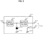
- FIG. 2 shows an example circuit structure of the rectifier circuit 310 in Embodiment 1.
- the rectifier circuit 310 in this example is a single shunt rectifier as shown in FIG. 2 .
- the rectifier circuit 310 includes an input filter 316, a rectifier element 314, and an output filter 317 between an input terminal 315 and the DC positive electrode 312.
- the rectifier element 314 has one end connected between the input filter 316 and the output filter 317 and the other end connected to the GND conductor 410.
- the rectifier element 314 is connected to have the polarity of outputting a positive DC voltage.
- the rectifier element 314 is, for example, a diode.
- the DC negative electrode 311 is connected to the GND conductor 410 through the through-hole 313.
- the DC positive electrode 312 has a higher potential than the DC negative electrode 311.
- the input filter 316 reduces harmonics generated during rectification.
- the output filter 317 is a smoothing filter and reduces harmonics generated during
- FIG. 3 shows an example circuit structure of the rectifier circuit 320 in Embodiment 1.
- the rectifier circuit 320 in this example is a single shunt rectifier as shown in FIG. 3 .
- the rectifier circuit 320 includes an input filter 326, a rectifier element 324, and an output filter 327 between an input terminal 325 and the DC positive electrode 322.
- the rectifier element 324 has one end connected between the input filter 326 and the output filter 327 and the other end connected to the GND conductor 420.
- the rectifier element 324 is connected to have the polarity of outputting a positive DC voltage.
- the rectifier element 324 is, for example, a diode.
- the DC negative electrode 321 is connected to the GND conductor 420 through the through-hole 323.
- the DC positive electrode 322 has a higher potential than the DC negative electrode 321.
- the input filter 326 reduces harmonics generated during rectification.
- the output filter 327 is a smoothing filter and reduces harmonics generated
- FIG. 4 is a schematic diagram of the rectenna device including the first rectifier 31 and the second rectifier 32 that are connected in series.
- a DC wire 600 connects the DC positive electrode 312 for the rectifier circuit 310 to the DC negative electrode 321 for the rectifier circuit 320.
- a DC wire 601 connects the DC negative electrode 311 for the rectifier circuit 310 to one end of a load 7.
- a DC wire 602 connects the DC positive electrode 322 for the rectifier circuit 320 to the other end of the load 7.
- the rectifier circuit 310 and the rectifier circuit 320 are thus connected in series. In other words, the first rectifier 31 and the second rectifier 32 are connected in series.
- the capacitive coupler 5 forms an open circuit in response to direct current.
- the GND conductors 410 and 420 are electrically fully disconnected from each other while direct current is being provided.
- the GND conductors 410 and 420 have different potentials. This allows the rectifier circuit 310 (first rectifier 31) and the rectifier circuit 320 (second rectifier 32) to be connected in series.
- the rectenna device receives incoming radio frequency waves with the antenna 210 and feeds the radio frequency waves through the slot into the rectifier circuit 310, and receives incoming radio frequency waves with the antenna 220 and feeds the waves through the slot into the rectifier circuit 320. More specifically, the radio frequency waves received with the antenna 210 is fed into the rectifier circuit 310 through the slot 411, whereas the radio frequency waves received with the antenna 220 is fed into the rectifier circuit 320 through the slot 421.
- the rectifier element 314 In response to the radio frequency waves input into the input terminal 315 in the rectifier circuit 310 shown in FIG. 2 , the rectifier element 314 turns on and off repeatedly in every half cycle, generating high-order harmonics and an offset voltage in the direction corresponding to the polarity of the rectifier element 314. This offset voltage is a DC voltage.
- the voltage waveform then undergoes a Fourier transform to show direct current and high-order harmonics.
- the waveform is then processed through the input filter 316 and the output filter 317 to reduce harmonics.
- the rectifier element 314 thus performs a class-F operation to achieve highly efficient RF-DC conversion.
- the GND conductor 410 and the DC negative electrode 311 for the rectifier circuit 310 are connected through the through-hole 313.
- the output filter 317 smooths the waveform of the voltage generated by the rectifier element 314 and outputs a positive DC voltage V DC1 between the DC negative electrode 311 and the DC positive electrode 312 for the rectifier circuit 310.
- the rectifier circuit 320 shown in FIG. 3 operates in the same manner as the rectifier circuit 310.
- the rectifier element 324 turns on and off repeatedly in every half cycle, generating high-order harmonics and an offset voltage in the direction corresponding to the polarity of the rectifier element 324.
- This offset voltage is a DC voltage.
- the voltage waveform then undergoes a Fourier transform to show DC and high-order harmonics.
- the waveform is then processed through the input filter 326 and the output filter 327 to reduce harmonics.
- the rectifier element 324 thus performs a class-F operation to achieve highly efficient RF-DC conversion.
- the GND conductor 420 and the DC negative electrode 321 for the rectifier circuit 320 are connected through the through-hole 323.
- the output filter 327 smooths the waveform of the voltage generated by the rectifier element 324 and outputs a positive DC voltage V DC2 between the DC negative electrode 321 and the DC positive electrode 322 for the rectifier circuit 320.
- the rectifier circuit 310 and the rectifier circuit 320 are connected in series.
- the load 7 thus receives the sum (V DC1 + V DC2 ) of the DC voltage V DC1 resulting from the RF-DC conversion performed by the rectifier circuit 310 in the first rectifier 31 and the DC voltage V DC2 resulting from the RF-DC conversion performed by the rectifier circuit 320 in the second rectifier 32.
- the rectifier circuits 310 and 320 that are series-connected can double the voltage applied to the load 7 and halve the current flowing through the load 7, as compared with when they are parallel-connected, with the load 7 receiving the same power.
- the series-connected circuits allow less direct current to flow than parallel-connected circuit, and cause less output voltage drop in the DC wires 600 to 602. The rectenna device can thus be highly efficient.
- the series-connected circuits reduce the direct current supplied to the load 7.
- the DC wires 600 to 602 can be wires with a smaller current capacity. With a small conductor area, the DC wires can be lightweight. The rectenna device can thus be lighter.
- the GND conductor is to absorb all the electric force lines of the fundamental waves generated from the antenna toward the GND conductor.
- a GND conductor with a greater area can absorb more electric force lines of the fundamental waves.
- FIG. 5 is a conceptual diagram describing the electric force lines of the fundamental waves generated between the antenna 210 and the GND conductor 410 without the capacitive coupler 5.
- the dielectric 1 is not shown, and the electric force lines are shown clearly.
- the electric force lines of the fundamental waves generated between the antenna 210 and the GND conductor 410 spread to the area of the GND conductor 420, as well as to the GND conductor 410. Without the capacitive coupler 5, the GND conductors 410 and 420 have different potentials. Thus, the GND conductor 410 alone absorbs the fundamental waves generated from the antenna 210. Without all the generated electric force lines of the fundamental waves being absorbed, the antenna 210 has a lower antenna gain for the fundamental waves.
- the electric force lines of the fundamental waves generated from the antenna 220 spread to the area of the GND conductor 410, as well as to the GND conductor 420. Without the capacitive coupler 5, the GND conductors 410 and 420 have different potentials. Thus, the GND conductor 420 alone absorbs the fundamental waves generated from the antenna 220. Without all the generated electric force lines of the fundamental waves being absorbed, the antenna 220 has a lower antenna gain for the fundamental waves.
- FIG. 6 is a conceptual diagram showing the electric force lines of the fundamental waves generated between the antenna 210 and the GND conductors 410 and 420 with the capacitive coupler 5.
- the dielectric 1 is not shown, and the electric force lines are shown clearly.
- the electric force lines of the fundamental waves generated between the antenna 210 and the GND conductor 410 spread also to the area of the GND conductor 420 as well as to the GND conductor 410.
- the capacitive coupler 5, forming a short circuit in response to the fundamental waves, causes the GND conductors 410 and 420 to be virtually equipotential for the fundamental waves.
- the GND conductors thus virtually extend across the board surface for the fundamental waves.
- the GND conductors 410 and 420 are virtually electrically connected with each other for the fundamental waves. This increases the apparent area of the GND conductors, relative to the antenna 210.
- the GND conductors 410 and 420 can both absorb the fundamental waves generated from the antenna 210.
- the antenna 210 thus achieves a high antenna gain for the fundamental waves.
- the electric force lines of the fundamental waves generated from the antenna 220 spread also to the area of the GND conductor 410 as well as to the GND conductor 420. This increases the apparent area of the GND conductors, relative to the antenna 220.
- the GND conductors 410 and 420 can both absorb the fundamental waves generated from the antenna 220.
- the antenna 220 achieves a high antenna gain for the fundamental waves.
- the rectenna device causes less voltage drop in the DC wires 600 to 602 while maintaining a high antenna gain for the fundamental waves, thus achieving higher efficiency.
- the DC wires 600 to 602 can also be lighter.
- FIG. 7 is a diagram of a configuration of a rectenna device including three rectifiers. As shown in FIG. 7 , the rectenna device further includes a third rectifier 33, an antenna 230 (third antenna), and a capacitive coupler 5 (second capacitive coupler). The third rectifier 33 is adjacent to the second rectifier 32. The third rectifier 33 has the same structure as the first rectifier 31 and the second rectifier 32, and thus is not described in detail.
- the third rectifier 33 includes a rectifier circuit 330 and a GND conductor 430 (third ground conductor).
- the GND conductor 430 serves as a reference potential for the antenna 230 and the rectifier circuit 330.
- the rectifier circuit board 300 includes a DC negative electrode 331 and a DC positive electrode 332 for the rectifier circuit 330.
- the DC negative electrode 331 is connected to the GND conductor 430 through a through-hole 333.
- the GND conductor 430 has a slot 431 facing the antenna 230.
- the slot 431 extends through the GND conductor 430.
- the GND conductor 420 (second ground conductor) and the GND conductor 430 (third ground conductor) are connected with the capacitive coupler 5 (second capacitive coupler) in between.
- the rectifier circuit 320 and the rectifier circuit 330 are connected in series. In other words, the second rectifier 32 and the third rectifier 33 are connected in series.
- the capacitive coupler 5 is located between GND conductors in adjacent rectifiers.
- the GND conductors in adjacent rectifiers are connected with the capacitive coupler 5 in between.
- the rectenna device including three or more rectifiers includes the capacitive couplers 5 that form an open circuit in response to direct current and form a short circuit in response to the fundamental waves.
- the capacitive couplers 5 each are located between adjacent ones of the GND conductors 410, 420, and 430 to enable series connection of the multiple rectifiers. This structure causes less voltage drop in the DC wires while maintaining a high antenna gain for the fundamental waves, thus achieving higher efficiency.
- the DC wires can also be lighter.
- a rectenna device may include more rectifiers to achieve still higher efficiency and be lighter.
- the rectenna device may be suitable for, for example, space solar power systems (SSPS) or other large rectenna systems with an output power of several thousand kilowatts that include many rectifiers.
- SSPS space solar power systems
- FIG. 8 is a diagram of a configuration of a rectenna device according to Embodiment 2 of the present disclosure.
- the present embodiment focuses on the structure of the capacitive coupler 5.
- the capacitive coupler 5 includes an interdigital capacitor 510.
- the other components are substantially the same as those in the rectenna apparatus according to Embodiment 1, and will not be described. The same components are given the same reference numerals.
- the interdigital capacitor 510 is a coupler including an elongated metal pattern located between the adjacent GND conductors 410 and 420.
- the GND conductors 410 and 420 are connected with the interdigital capacitor 510 in between.
- the interdigital capacitor 510 includes needle-shaped metal pieces alternately arranged near the GND conductor 410 and the GND conductor 420. This structure can generate capacitance between the needle-shaped elongated metal pieces. The capacitance value may be set as appropriate by changing the intervals between the needle-shaped metal pieces, the length of the metal pattern, and the number of needle-shaped metal pieces in the metal pattern.
- the interdigital capacitor 510 in this example has the pattern that forms a short circuit between the GND conductors 410 and 420 in response to the fundamental waves.
- the interdigital capacitor 510 has the needle-shaped metal pieces physically separated apart. An open circuit is thus formed between the GND conductors 410 and 420 in response to direct current. The capacitance value is set to cause a short circuit between the GND conductors 410 and 420 in response to the fundamental waves.
- the rectifier circuit 310 in the first rectifier 31 and the rectifier circuit 320 in the second rectifier 32 can be connected in series.
- the rectenna device according to Embodiment 2 thus causes less voltage drop in the DC wires while maintaining a high antenna gain for the fundamental waves, thus achieving higher efficiency.
- the DC wires can also be lighter.
- FIG. 9 is a diagram of a configuration of another rectenna device according to Embodiment 2.
- the rectenna device shown in FIG. 9 includes the capacitive coupler 5 including a chip capacitor 520.
- the interdigital capacitor 510 in the rectenna device shown in FIG. 8 is replaced by the chip capacitor 520.
- the chip capacitor 520 is located between the adjacent GND conductors 410 and 420.
- the GND conductors 410 and 420 are connected with the chip capacitor 520 in between.
- the chip capacitor 520 forms an open circuit between the GND conductors 410 and 420 in response to direct current.
- the chip capacitor 520 has a capacitance value set to cause a short circuit between the GND conductors 410 and 420 in response to the fundamental waves.
- the rectifier circuit 310 in the first rectifier 31 and the rectifier circuit 320 in the second rectifier 32 can be connected in series.
- the rectenna device with the above structure also causes less voltage drop in the DC wires while maintaining a high antenna gain for the fundamental waves, thus achieving higher efficiency.
- the DC wires can also be lighter.
- the rectenna device shown in FIG. 9 includes the single chip capacitor 520, the rectenna device may include multiple chip capacitors.
- the rectenna device shown in FIG. 8 includes the capacitive coupler 5 including the single interdigital capacitor 510
- the rectenna device shown in FIG. 9 includes the capacitive coupler 5 including the single chip capacitor 520.
- the capacitive coupler 5 may include at least one interdigital capacitor 510 or at least one chip capacitor 520.
- the capacitive coupler 5 may include one interdigital capacitor 510 and one chip capacitor 520 in combination.
- the capacitive coupler 5 may include multiple interdigital capacitors 510 and multiple chip capacitors 520 in combination.
- FIG. 10 is a diagram of a configuration of a rectenna device according to Embodiment 3 of the present disclosure.
- the rectenna device according to Embodiment 3 of the present disclosure includes a rectifier including multiple rectifier circuits.
- the rectenna device shown in FIG. 10 includes a second rectifier 32 including multiple rectifier circuits 320 and 324.
- the rectenna device includes an antenna 210 (first antenna), an antenna 220 (second antenna), an antenna 221 (second antenna), a first rectifier 31, a second rectifier 32, a dielectric 1, and a capacitive coupler 5.
- the first rectifier 31 includes a rectifier circuit 310 (first rectifier circuit) and a GND conductor (first ground conductor) 410.
- the second rectifier 32 includes a rectifier circuit 320 (second rectifier circuit), a rectifier circuit 324 (second rectifier circuit), and a GND conductor 420 (second ground conductor).
- the first rectifier 31 and the second rectifier 32 are adjacent to each other.
- the second rectifier 32 differs from the second rectifier 32 in Embodiment 1 in including two rectifier circuits 320 and 324.
- the rectenna device in Embodiment 3 differs from the rectenna device in Embodiment 1 in further including the antenna 221 and the rectifier circuit 324.
- the other components are substantially the same as those in Embodiment 1, and will not be described. The same components are given the same reference numerals.
- the antenna 221 receives input radio frequency waves. As shown in FIG. 10 , the antenna 221 is adjacent to the antenna 220 on an antenna board 200.
- the rectifier circuit 324 converts the radio frequency waves input in the antenna 221 into direct current.
- the rectifier circuit 324 is adjacent to the rectifier circuit 320 on a rectifier circuit board 300.
- the rectifier circuit board 300 includes a DC negative electrode 325 and a DC positive electrode 326 for receiving direct current generated by the rectifier circuit 324.
- the rectifier circuit 324 is located between the DC negative electrode 325 and the DC positive electrode 326 in the example shown in FIG. 10 , but may be located differently.
- the DC positive electrode 326 has a higher potential than the DC negative electrode 325.
- the GND conductor 420 serves as a reference potential for the antenna 221 and the rectifier circuit 324, and for the antenna 220 and the rectifier circuit 320.
- the GND conductor 420 is located on a surface of the rectifier circuit board 300 opposite to the surface on which the rectifier circuits 320 and 324 are located.
- the rectifier circuit board 300 has a through-hole 327.
- the DC negative electrode 325 for the rectifier circuit 324 is connected to the GND conductor 420 through the through-hole 327. In other words, the DC negative electrode 321 for the rectifier circuit 320 and the DC negative electrode 325 for the rectifier circuit 324 are equipotential through the GND conductor 420.
- the surface of the antenna board 200 to which the dielectric 1 is bonded faces the surface of the rectifier circuit board 300 on which the GND conductors 410 and 420 are located.
- the antenna board 200 is bonded to one surface of the dielectric 1, and the rectifier circuit 310 and the rectifier circuit 320 and 324 are bonded to the other surface of the dielectric 1 with the GND conductors 410 and 420 in between.
- the GND conductor 420 has a slot 422 facing the antenna 221.
- the slot 422 extends through the GND conductor 420.
- the slot 422 allows slot coupling of the antenna 221 to the rectifier circuit 324.
- the rectifier circuit 324 is a single-shunt rectifier with the same structure as the rectifier circuits 310 and 320 (not shown).
- FIG. 11 is a schematic diagram describing the connection between the rectifier circuit 310, the rectifier circuit 320, and the rectifier circuit 324 in the rectenna device according to Embodiment 3.
- a DC wire 600 connects the DC negative electrode 321 serving as a common reference electrode for the rectifier circuits 320 and 324 to the DC positive electrode 312 for the rectifier circuit 310.
- a DC wire 603 connects the DC positive electrode 322 for the rectifier circuit 320 to the DC positive electrode 326 for the rectifier circuit 324.
- a DC wire 601 connects the DC negative electrode 311 for the rectifier circuit 310 to one end of a load 7, and a DC wire 602 connects the DC positive electrode 326 for the rectifier circuit 324 to the other end of the load 7.
- the rectifier circuits 320 and 324 commonly use the GND conductor 420 as a reference potential and are restricted to parallel connection. More specifically, the rectifier circuits 320 and 324 are connected in parallel, and the parallel-connected rectifier circuits 320 and 324 are connected in series to the rectifier circuit 310.
- the capacitive coupler 5 forms an open circuit in response to direct current.
- the GND conductors 410 and 420 are electrically fully disconnected from each other while direct current is being provided.
- the GND conductors 410 and 420 have different potentials. This allows serial connection between the rectifier circuit 310 in the first rectifier 31 and the rectifier circuits 320 and 324 in the second rectifier 32.
- the rectenna device receives incoming radio frequency waves with the antennas 210, 220, and 221 and feeds the radio frequency waves into the corresponding rectifier circuits 310, 320, and 324 through the corresponding slots 411, 421, and 422. More specifically, the radio frequency waves received with the antenna 210 are fed into the rectifier circuit 310 through the slot 411. The radio frequency waves received with the antenna 220 are fed into the rectifier circuit 320 through the slot 421. The radio frequency waves received with the antenna 221 are fed into the rectifier circuit 324 through the slot 422.
- the radio frequency waves fed through the slot into the rectifier circuit 310 undergo RF-DC conversion to output the resultant positive DC voltage V DC1 between the DC negative electrode 311 and the DC positive electrode 312.
- the first rectifier 31 outputs the DC voltage V DC1 from the rectifier circuit 310.
- the radio frequency waves fed through the slot into the rectifier circuit 320 undergo RF-DC conversion to output the resultant positive DC voltage V DC2 between the DC negative electrode 321 and the DC positive electrode 322.
- the radio frequency waves fed through the slot into the rectifier circuit 324 undergo RF-DC conversion to output the resultant positive DC voltage V DC3 between the DC negative electrode 321 and the DC positive electrode 326.
- the output voltage between the DC negative electrode 321 and the DC positive electrode 326 is the average voltage (V DC2 + V DC3 )/2 of the DC output voltage V DC2 from the rectifier circuit 320 and the DC output voltage V DC3 from the rectifier circuit 324.
- the second rectifier 32 outputs the average voltage (V DC2 + V DC3 )/2 of the DC output voltage V DC2 from the rectifier circuit 320 and the DC output voltage V DC3 from the rectifier circuit 324.
- the rectifier circuit 310 is connected in series to the parallel-connected rectifier circuits 320 and 324.
- the load 7 thus receives a DC voltage that is the sum (V DC1 + (V DC2 + V DC3 )/2) of the DC voltage V DC1 resulting from the RF-DC conversion performed by the rectifier circuit 310 in the first rectifier 31 and the average voltage (V DC2 + V DC3 )/2 resulting from the RF-DC conversion performed by the rectifier circuits 320 and 324 in the second rectifier 32.
- the structure of connecting the rectifier circuit 310 in the first rectifier 31 in series to the parallel-connected rectifier circuits 320 and 324 in the second rectifier 32 allows less current to flow through the load than the structure of connecting all the rectifier circuits 310, 320, and 324 in parallel.
- the circuits allow less direct current to flow through the load, and causes less output voltage drop in the DC wires 600 to 603. The rectenna device can thus be highly efficient.
- the DC wires 600 to 603 can be lightweight.
- the rectenna device can thus be lighter.
- the capacitive coupler 5 physically separates the GND conductors 410 and 420 from each other, the capacitive coupler 5 that forms a short circuit in response to the fundamental waves allows the GND conductors 410 and 420 to be virtually equipotential in response to the fundamental waves. In other words, the GND conductors 410 and 420 are virtually electrically connected with each other for the fundamental waves.
- the GND conductors 410 and 420 can both absorb the fundamental waves generated from the antenna 210.
- the antenna 210 thus achieves a high antenna gain for the fundamental waves.
- the antenna 220 and the antenna 221 achieve a high antenna gain for the fundamental waves.
- the rectenna device causes less voltage drop in the DC wires 600 to 603 while maintaining a high antenna gain of the antennas 210, 220, and 221 for the fundamental waves, thus achieving higher efficiency.
- the DC wires 600 to 603 can also be lighter.
- the rectenna device according to Embodiment 3 includes the second rectifier 32 including two rectifier circuits connected in parallel, the second rectifier 32 may include three or more rectifier circuits connected in parallel.
- the first rectifier 31 may include multiple rectifier circuits connected in parallel.
- Each of the first rectifier 31 and the second rectifier 32 may include multiple rectifier circuits connected in parallel.
- the rectenna device may include three or more rectifiers.
- FIG. 12 is a diagram of a configuration of a rectenna device including three rectifiers. As shown in FIG. 12 , the rectenna device further includes a third rectifier 33, an antenna 230 (third antenna), and a capacitive coupler 5 (second capacitive coupler). The third rectifier 33 is adjacent to the second rectifier 32. The third rectifier 33 has the same structure as the first and second rectifiers 31 and 32.
- the third rectifier 33 includes a rectifier circuit 330 and a GND conductor 430 (third ground conductor).
- the GND conductor 430 serves as a reference potential for the antenna 230 and the rectifier circuit 330.
- the rectifier circuit board 300 includes a DC negative electrode 331 and a DC positive electrode 332 for the rectifier circuit 330.
- the DC negative electrode 331 is connected to the GND conductor 430 through a through-hole 333.
- the GND conductor 430 has a slot 431 facing the antenna 230.
- the slot 431 extends through the GND conductor 430.
- the GND conductor 420 (second ground conductor) and the GND conductor 430 (third ground conductor) are connected with the capacitive coupler 5 (second capacitive coupler) in between.
- the rectifier circuit 320 and the rectifier circuit 330 are connected in series. In other words, the second rectifier 32 and the third rectifier 33 are connected in series.
- the capacitive couplers 5 are located between GND conductors in adjacent rectifiers.
- the GND conductors in adjacent rectifiers are connected with the capacitive coupler 5 in between.
- This structure enables series connection of multiple rectifiers. Any number of sets of series-connected or parallel-connected rectifier circuits may be combined in any manner to include at least one set of series-connected rectifier circuits.
- the rectenna device including three or more rectifiers includes the capacitive couplers 5 that form an open circuit in response to direct current and form a short circuit in response to the fundamental waves.
- the capacitive couplers 5 each are located between adjacent ones of the GND conductors to enable series connection of the multiple rectifiers. This structure causes less voltage drop in the DC wires while maintaining a high antenna gain for the fundamental waves, thus achieving higher efficiency.
- the DC wires can also be lighter.
- the rectenna device may include more rectifiers to achieve still higher efficiency and be lighter.
- the rectenna device may be suitable for, for example, SSPS or other large rectenna systems with an output power of several thousand kilowatts that include many rectifiers.
- the capacitive couplers 5 may each include, in the same manner as in Embodiment 2, the interdigital capacitor 510 shown in FIG. 8 or the chip capacitor 520 shown in FIG. 9 .
- the capacitive couplers 5 may each include one interdigital capacitor 510 and one chip capacitor 520 in combination.
- the capacitive couplers 5 may each include multiple interdigital capacitors 510 and multiple chip capacitors 520 in combination.
Landscapes
- Engineering & Computer Science (AREA)
- Computer Networks & Wireless Communication (AREA)
- Power Engineering (AREA)
- Physics & Mathematics (AREA)
- Electromagnetism (AREA)
- Waveguide Aerials (AREA)
- Details Of Aerials (AREA)
- Input Circuits Of Receivers And Coupling Of Receivers And Audio Equipment (AREA)
Abstract
Description
- The present disclosure relates to a rectenna device that converts radio frequency waves into direct current power.
- A rectenna (rectifying antenna) device is an antenna device with a rectifier circuit. The rectenna device converts radio frequency waves input in the antenna device into direct current (DC) through RF-DC conversion using the rectifier circuit. A rectenna device to be mounted on a power receiver for space solar power systems (SSPS) has recently been under development. A rectenna device including an array of rectenna elements is used preferably for feeding high DC power to a load after receiving high-power radio frequency waves with an antenna and performing highly efficient RF-DC conversion with a rectifier circuit. Rectenna devices that are lightweight and have higher efficiency have thus been awaited.
- A known rectenna device including rectenna elements includes an antenna bonded to one surface of a dielectric and a rectifier circuit bonded to the other surface of the dielectric with a ground (GND) conductor in between. In one design, the GND conductor is provided on a bonding surface of the back surface of the rectifier circuit that is bonded to the dielectric, and serves as a common GND for the antenna and for the rectifier circuit. The rectenna device including the rectenna elements has the GND commonly used by each rectenna element to achieve a high antenna gain. The GND conductor thus has a large area (see, for example, Patent Literature 1).
- Patent Literature 1: Unexamined
Japanese Patent Application Publication No. 2018-107562 - Although the rectenna elements and the rectenna device described in
Patent Literature 1 achieve a high antenna gain with the GND conductor with a large area, each rectifier circuit has a common GND potential. The rectifier circuits are restricted to parallel connection and have a high resultant direct current in the output power. This causes more voltage drop in DC wires and reduces efficiency. - In response to the above issue, an objective of the present disclosure is to provide a rectenna device that causes less voltage drop in DC wires while maintaining a high antenna gain for fundamental waves.
- A rectenna device according to an aspect of the present disclosure includes a first antenna, a first rectifier to rectify a radio frequency wave input in the first antenna, a second antenna, a second rectifier to rectify a radio frequency wave input in the second antenna, and a first capacitive coupler to form an open circuit in response to direct current and to form a short circuit in response to a fundamental wave. The first rectifier includes a first ground conductor to be a reference potential. The second rectifier includes a second ground conductor to be a reference potential. The first ground conductor and the second ground conductor are connected with the first capacitive coupler in between. The first rectifier and the second rectifier are connected in series.
- The rectenna device according to the above aspect of the present disclosure causes less voltage drop in DC wires while maintaining a high antenna gain for fundamental waves.
-
-
FIG. 1 is a diagram of a configuration of a rectenna device according toEmbodiment 1 of the present disclosure; -
FIG. 2 is a block diagram of a first rectifier according toEmbodiment 1 of the present disclosure, showing an example circuit structure; -
FIG. 3 is a block diagram of a second rectifier according toEmbodiment 1 of the present disclosure, showing an example circuit structure; -
FIG. 4 is a schematic diagram describing the connection between rectifier circuits in the rectenna device according toEmbodiment 1 of the present disclosure; -
FIG. 5 is a conceptual diagram of electric force lines of fundamental waves generated between an antenna and a GND conductor without a capacitive coupler; -
FIG. 6 is a conceptual diagram of electric force lines of fundamental waves generated between the antenna and GND conductors with a capacitive coupler; -
FIG. 7 is a diagram of a configuration of the rectenna device according toEmbodiment 1 of the present disclosure including three rectifiers; -
FIG. 8 is a diagram of a configuration of a rectenna device according toEmbodiment 2 of the present disclosure; -
FIG. 9 is a diagram of another configuration of the rectenna device according toEmbodiment 2 of the present disclosure; -
FIG. 10 is a diagram of a configuration of a rectenna device according to Embodiment 3 of the present disclosure; -
FIG. 11 is a schematic diagram describing the connection between rectifier circuits in the rectenna device according to Embodiment 3 of the present disclosure; and -
FIG. 12 is a diagram of a configuration of the rectenna device according to Embodiment 3 of the present disclosure including three rectifiers. - A rectenna device according to one or more embodiments of the present disclosure will now be described in detail with reference to the drawings. Throughout the drawings, the same or equivalent components are given the same reference numerals.
-
FIG. 1 is a diagram of a configuration of a rectenna device according toEmbodiment 1 of the present disclosure. The rectenna device shown inFIGS. 1 to 6 includes two rectifiers.FIG. 7 shows a rectenna device including three rectifiers. The rectenna device inFIGS. 1 to 6 includes an antenna 210 (first antenna), an antenna 220 (second antenna), afirst rectifier 31, asecond rectifier 32, a dielectric 1, and a capacitive coupler 5 (first capacitive coupler). Thefirst rectifier 31 includes a rectifier circuit (first rectifier circuit) 310 and a ground (GND) conductor 410 (first ground conductor). Thesecond rectifier 32 includes a rectifier circuit (second rectifier circuit) 320 and a GND conductor 420 (second ground conductor). Thefirst rectifier 31 and thesecond rectifier 32 are adjacent to each other. - The
antenna 210 and theantenna 220 receive input radio frequency waves. In this example, input radio frequency waves include waves in a microwave band. As shown inFIG. 1 , theantenna 210 and theantenna 220 are adjacent to each other on anantenna board 200. Theantenna board 200 has the dielectric 1 bonded to one surface. - Through RF-DC conversion, the
rectifier circuit 310 converts radio frequency (RF) waves input in theantenna 210 into direct current, and therectifier circuit 320 converts RF waves input in theantenna 220 into direct current. Therectifier circuit 310 and therectifier circuit 320 are located on arectifier circuit board 300. Therectifier circuit board 300 includes a direct current (DC)negative electrode 311 and a DCpositive electrode 312 for outputting direct current generated by therectifier circuit 310. Therectifier circuit 310 is located between the DCnegative electrode 311 and the DCpositive electrode 312 in the example shown inFIG. 1 , but may be located differently. Therectifier circuit board 300 includes a DCnegative electrode 321 and a DCpositive electrode 322 for outputting direct current generated by therectifier circuit 320. Therectifier circuit 320 is located between the DCnegative electrode 321 and the DCpositive electrode 322 in the example shown inFIG. 1 , but may be located differently. - The
GND conductor 410 serves as a reference potential for theantenna 210 and therectifier circuit 310. TheGND conductor 410 is located on a surface of therectifier circuit board 300 opposite to the surface on which therectifier circuit 310 is located. TheGND conductor 420 serves as a reference potential for theantenna 220 and therectifier circuit 320. TheGND conductor 420 is located on a surface of therectifier circuit board 300 opposite to the surface on which therectifier circuit 320 is located. - The
rectifier circuit board 300 has a through-hole 313. The DCnegative electrode 311 for therectifier circuit 310 is connected to theGND conductor 410 through the through-hole 313. Therectifier circuit 310 outputs power between the DCnegative electrode 311 and the DCpositive electrode 312. The DCpositive electrode 312 has a higher potential than the DCnegative electrode 311. Therectifier circuit board 300 has a through-hole 323. The DCnegative electrode 321 for therectifier circuit 320 is connected to theGND conductor 420 through the through-hole 323. Therectifier circuit 320 outputs power between the DCnegative electrode 321 and the DCpositive electrode 322. The DCpositive electrode 322 has a higher potential than the DCnegative electrode 321. - The surface of the
antenna board 200 to which thedielectric 1 is bonded faces the surface of therectifier circuit board 300 on which theGND conductors antenna board 200 is bonded to one surface of the dielectric 1, and therectifier circuit 310 and therectifier circuit 320 are bonded to the other surface of the dielectric 1 with theGND conductors - The
GND conductor 410 has aslot 411 facing theantenna 210. Theslot 411 extends through theGND conductor 410. Theslot 411 allows slot coupling of theantenna 210 to therectifier circuit 310. TheGND conductor 420 has aslot 421 facing theantenna 220. Theslot 421 extends through theGND conductor 420. Theslot 421 allows slot coupling of theantenna 220 to therectifier circuit 320. - The
capacitive coupler 5 is a coupler that forms an open circuit in response to direct current and forms a short circuit in response to fundamental waves. Thecapacitive coupler 5 is located between theGND conductor 410 and theGND conductor 420. In other words, theGND conductors capacitive coupler 5. -
FIG. 2 shows an example circuit structure of therectifier circuit 310 inEmbodiment 1. Therectifier circuit 310 in this example is a single shunt rectifier as shown inFIG. 2 . Therectifier circuit 310 includes aninput filter 316, arectifier element 314, and anoutput filter 317 between aninput terminal 315 and the DCpositive electrode 312. Therectifier element 314 has one end connected between theinput filter 316 and theoutput filter 317 and the other end connected to theGND conductor 410. Therectifier element 314 is connected to have the polarity of outputting a positive DC voltage. Therectifier element 314 is, for example, a diode. The DCnegative electrode 311 is connected to theGND conductor 410 through the through-hole 313. The DCpositive electrode 312 has a higher potential than the DCnegative electrode 311. Theinput filter 316 reduces harmonics generated during rectification. Theoutput filter 317 is a smoothing filter and reduces harmonics generated during rectification. -
FIG. 3 shows an example circuit structure of therectifier circuit 320 inEmbodiment 1. Therectifier circuit 320 in this example is a single shunt rectifier as shown inFIG. 3 . Therectifier circuit 320 includes aninput filter 326, arectifier element 324, and anoutput filter 327 between aninput terminal 325 and the DCpositive electrode 322. Therectifier element 324 has one end connected between theinput filter 326 and theoutput filter 327 and the other end connected to theGND conductor 420. Therectifier element 324 is connected to have the polarity of outputting a positive DC voltage. Therectifier element 324 is, for example, a diode. The DCnegative electrode 321 is connected to theGND conductor 420 through the through-hole 323. The DCpositive electrode 322 has a higher potential than the DCnegative electrode 321. Theinput filter 326 reduces harmonics generated during rectification. Theoutput filter 327 is a smoothing filter and reduces harmonics generated during rectification. -
FIG. 4 is a schematic diagram of the rectenna device including thefirst rectifier 31 and thesecond rectifier 32 that are connected in series. As shown inFIG. 4 , aDC wire 600 connects the DCpositive electrode 312 for therectifier circuit 310 to the DCnegative electrode 321 for therectifier circuit 320. ADC wire 601 connects the DCnegative electrode 311 for therectifier circuit 310 to one end of aload 7. ADC wire 602 connects the DCpositive electrode 322 for therectifier circuit 320 to the other end of theload 7. Therectifier circuit 310 and therectifier circuit 320 are thus connected in series. In other words, thefirst rectifier 31 and thesecond rectifier 32 are connected in series. - The
capacitive coupler 5 forms an open circuit in response to direct current. Thus, theGND conductors GND conductors - The operation of the rectenna device according to
Embodiment 1 of the present disclosure will now be described. The rectenna device receives incoming radio frequency waves with theantenna 210 and feeds the radio frequency waves through the slot into therectifier circuit 310, and receives incoming radio frequency waves with theantenna 220 and feeds the waves through the slot into therectifier circuit 320. More specifically, the radio frequency waves received with theantenna 210 is fed into therectifier circuit 310 through theslot 411, whereas the radio frequency waves received with theantenna 220 is fed into therectifier circuit 320 through theslot 421. - In response to the radio frequency waves input into the
input terminal 315 in therectifier circuit 310 shown inFIG. 2 , therectifier element 314 turns on and off repeatedly in every half cycle, generating high-order harmonics and an offset voltage in the direction corresponding to the polarity of therectifier element 314. This offset voltage is a DC voltage. The voltage waveform then undergoes a Fourier transform to show direct current and high-order harmonics. The waveform is then processed through theinput filter 316 and theoutput filter 317 to reduce harmonics. Therectifier element 314 thus performs a class-F operation to achieve highly efficient RF-DC conversion. TheGND conductor 410 and the DCnegative electrode 311 for therectifier circuit 310 are connected through the through-hole 313. Theoutput filter 317 smooths the waveform of the voltage generated by therectifier element 314 and outputs a positive DC voltage VDC1 between the DCnegative electrode 311 and the DCpositive electrode 312 for therectifier circuit 310. - The
rectifier circuit 320 shown inFIG. 3 operates in the same manner as therectifier circuit 310. In response to the radio frequency waves input into theinput terminal 325 in therectifier circuit 320, therectifier element 324 turns on and off repeatedly in every half cycle, generating high-order harmonics and an offset voltage in the direction corresponding to the polarity of therectifier element 324. This offset voltage is a DC voltage. The voltage waveform then undergoes a Fourier transform to show DC and high-order harmonics. The waveform is then processed through theinput filter 326 and theoutput filter 327 to reduce harmonics. Therectifier element 324 thus performs a class-F operation to achieve highly efficient RF-DC conversion. TheGND conductor 420 and the DCnegative electrode 321 for therectifier circuit 320 are connected through the through-hole 323. Theoutput filter 327 smooths the waveform of the voltage generated by therectifier element 324 and outputs a positive DC voltage VDC2 between the DCnegative electrode 321 and the DCpositive electrode 322 for therectifier circuit 320. - As shown in
FIG. 4 , therectifier circuit 310 and therectifier circuit 320 are connected in series. Theload 7 thus receives the sum (VDC1 + VDC2) of the DC voltage VDC1 resulting from the RF-DC conversion performed by therectifier circuit 310 in thefirst rectifier 31 and the DC voltage VDC2 resulting from the RF-DC conversion performed by therectifier circuit 320 in thesecond rectifier 32. - The
rectifier circuits load 7 and halve the current flowing through theload 7, as compared with when they are parallel-connected, with theload 7 receiving the same power. The series-connected circuits allow less direct current to flow than parallel-connected circuit, and cause less output voltage drop in theDC wires 600 to 602. The rectenna device can thus be highly efficient. - The series-connected circuits reduce the direct current supplied to the
load 7. In this case, theDC wires 600 to 602 can be wires with a smaller current capacity. With a small conductor area, the DC wires can be lightweight. The rectenna device can thus be lighter. - The antenna characteristics will now be described. To achieve a high antenna gain with the rectenna device, the GND conductor is to absorb all the electric force lines of the fundamental waves generated from the antenna toward the GND conductor. A GND conductor with a greater area can absorb more electric force lines of the fundamental waves.
-
FIG. 5 is a conceptual diagram describing the electric force lines of the fundamental waves generated between theantenna 210 and theGND conductor 410 without thecapacitive coupler 5. InFIG. 5 , thedielectric 1 is not shown, and the electric force lines are shown clearly. - As shown in
FIG. 5 , the electric force lines of the fundamental waves generated between theantenna 210 and theGND conductor 410 spread to the area of theGND conductor 420, as well as to theGND conductor 410. Without thecapacitive coupler 5, theGND conductors GND conductor 410 alone absorbs the fundamental waves generated from theantenna 210. Without all the generated electric force lines of the fundamental waves being absorbed, theantenna 210 has a lower antenna gain for the fundamental waves. - Similarly, the electric force lines of the fundamental waves generated from the
antenna 220 spread to the area of theGND conductor 410, as well as to theGND conductor 420. Without thecapacitive coupler 5, theGND conductors GND conductor 420 alone absorbs the fundamental waves generated from theantenna 220. Without all the generated electric force lines of the fundamental waves being absorbed, theantenna 220 has a lower antenna gain for the fundamental waves. -
FIG. 6 is a conceptual diagram showing the electric force lines of the fundamental waves generated between theantenna 210 and theGND conductors capacitive coupler 5. InFIG. 6 , thedielectric 1 is not shown, and the electric force lines are shown clearly. - As shown in
FIG. 6 , the electric force lines of the fundamental waves generated between theantenna 210 and theGND conductor 410 spread also to the area of theGND conductor 420 as well as to theGND conductor 410. Thecapacitive coupler 5, forming a short circuit in response to the fundamental waves, causes theGND conductors FIG. 6 , the GND conductors thus virtually extend across the board surface for the fundamental waves. In other words, theGND conductors antenna 210. Thus, theGND conductors antenna 210. Theantenna 210 thus achieves a high antenna gain for the fundamental waves. - Similarly, the electric force lines of the fundamental waves generated from the
antenna 220 spread also to the area of theGND conductor 410 as well as to theGND conductor 420. This increases the apparent area of the GND conductors, relative to theantenna 220. Thus, theGND conductors antenna 220. Thus, theantenna 220 achieves a high antenna gain for the fundamental waves. - The rectenna device according to
Embodiment 1 of the present disclosure causes less voltage drop in theDC wires 600 to 602 while maintaining a high antenna gain for the fundamental waves, thus achieving higher efficiency. TheDC wires 600 to 602 can also be lighter. - Although the rectenna device includes two rectifiers in
FIGS. 1 to 6 , the rectenna device may include three or more rectifiers.FIG. 7 is a diagram of a configuration of a rectenna device including three rectifiers. As shown inFIG. 7 , the rectenna device further includes athird rectifier 33, an antenna 230 (third antenna), and a capacitive coupler 5 (second capacitive coupler). Thethird rectifier 33 is adjacent to thesecond rectifier 32. Thethird rectifier 33 has the same structure as thefirst rectifier 31 and thesecond rectifier 32, and thus is not described in detail. - The
third rectifier 33 includes arectifier circuit 330 and a GND conductor 430 (third ground conductor). TheGND conductor 430 serves as a reference potential for theantenna 230 and therectifier circuit 330. Therectifier circuit board 300 includes a DCnegative electrode 331 and a DCpositive electrode 332 for therectifier circuit 330. The DCnegative electrode 331 is connected to theGND conductor 430 through a through-hole 333. TheGND conductor 430 has aslot 431 facing theantenna 230.
Theslot 431 extends through theGND conductor 430. The GND conductor 420 (second ground conductor) and the GND conductor 430 (third ground conductor) are connected with the capacitive coupler 5 (second capacitive coupler) in between. Therectifier circuit 320 and therectifier circuit 330 are connected in series. In other words, thesecond rectifier 32 and thethird rectifier 33 are connected in series. - For such a rectenna device including three or more rectifiers, the
capacitive coupler 5 is located between GND conductors in adjacent rectifiers. In other words, the GND conductors in adjacent rectifiers are connected with thecapacitive coupler 5 in between. This structure enables series connection of multiple rectifiers. - The rectenna device including three or more rectifiers includes the
capacitive couplers 5 that form an open circuit in response to direct current and form a short circuit in response to the fundamental waves. Thecapacitive couplers 5 each are located between adjacent ones of theGND conductors -
FIG. 8 is a diagram of a configuration of a rectenna device according toEmbodiment 2 of the present disclosure. The present embodiment focuses on the structure of thecapacitive coupler 5. In detail, thecapacitive coupler 5 includes aninterdigital capacitor 510. The other components are substantially the same as those in the rectenna apparatus according toEmbodiment 1, and will not be described. The same components are given the same reference numerals. - As shown in
FIG. 8 , theinterdigital capacitor 510 is a coupler including an elongated metal pattern located between theadjacent GND conductors GND conductors interdigital capacitor 510 in between. Theinterdigital capacitor 510 includes needle-shaped metal pieces alternately arranged near theGND conductor 410 and theGND conductor 420. This structure can generate capacitance between the needle-shaped elongated metal pieces. The capacitance value may be set as appropriate by changing the intervals between the needle-shaped metal pieces, the length of the metal pattern, and the number of needle-shaped metal pieces in the metal pattern. Theinterdigital capacitor 510 in this example has the pattern that forms a short circuit between theGND conductors - The
interdigital capacitor 510 has the needle-shaped metal pieces physically separated apart. An open circuit is thus formed between theGND conductors GND conductors Embodiment 1, therectifier circuit 310 in thefirst rectifier 31 and therectifier circuit 320 in thesecond rectifier 32 can be connected in series. - The rectenna device according to
Embodiment 2 thus causes less voltage drop in the DC wires while maintaining a high antenna gain for the fundamental waves, thus achieving higher efficiency. The DC wires can also be lighter. -
FIG. 9 is a diagram of a configuration of another rectenna device according toEmbodiment 2. The rectenna device shown inFIG. 9 includes thecapacitive coupler 5 including achip capacitor 520. In other words, theinterdigital capacitor 510 in the rectenna device shown inFIG. 8 is replaced by thechip capacitor 520. - As shown in
FIG. 9 , thechip capacitor 520 is located between theadjacent GND conductors GND conductors chip capacitor 520 in between. Thechip capacitor 520 forms an open circuit between theGND conductors chip capacitor 520 has a capacitance value set to cause a short circuit between theGND conductors Embodiment 1, therectifier circuit 310 in thefirst rectifier 31 and therectifier circuit 320 in thesecond rectifier 32 can be connected in series. - Similarly to the rectenna device shown in
FIG. 8 , the rectenna device with the above structure also causes less voltage drop in the DC wires while maintaining a high antenna gain for the fundamental waves, thus achieving higher efficiency. The DC wires can also be lighter. - Although the rectenna device shown in
FIG. 9 includes thesingle chip capacitor 520, the rectenna device may include multiple chip capacitors. - The rectenna device shown in
FIG. 8 includes thecapacitive coupler 5 including the singleinterdigital capacitor 510, and the rectenna device shown inFIG. 9 includes thecapacitive coupler 5 including thesingle chip capacitor 520. Thecapacitive coupler 5 may include at least oneinterdigital capacitor 510 or at least onechip capacitor 520. Thecapacitive coupler 5 may include oneinterdigital capacitor 510 and onechip capacitor 520 in combination. Thecapacitive coupler 5 may include multipleinterdigital capacitors 510 andmultiple chip capacitors 520 in combination. -
FIG. 10 is a diagram of a configuration of a rectenna device according to Embodiment 3 of the present disclosure. The rectenna device according to Embodiment 3 of the present disclosure includes a rectifier including multiple rectifier circuits. The rectenna device shown inFIG. 10 includes asecond rectifier 32 includingmultiple rectifier circuits first rectifier 31, asecond rectifier 32, adielectric 1, and acapacitive coupler 5. Thefirst rectifier 31 includes a rectifier circuit 310 (first rectifier circuit) and a GND conductor (first ground conductor) 410. Thesecond rectifier 32 includes a rectifier circuit 320 (second rectifier circuit), a rectifier circuit 324 (second rectifier circuit), and a GND conductor 420 (second ground conductor). Thefirst rectifier 31 and thesecond rectifier 32 are adjacent to each other. - The
second rectifier 32 differs from thesecond rectifier 32 inEmbodiment 1 in including tworectifier circuits Embodiment 1 in further including theantenna 221 and therectifier circuit 324. The other components are substantially the same as those inEmbodiment 1, and will not be described. The same components are given the same reference numerals. - The
antenna 221 receives input radio frequency waves. As shown inFIG. 10 , theantenna 221 is adjacent to theantenna 220 on anantenna board 200. - Through RF-DC conversion, the
rectifier circuit 324 converts the radio frequency waves input in theantenna 221 into direct current. Therectifier circuit 324 is adjacent to therectifier circuit 320 on arectifier circuit board 300. Therectifier circuit board 300 includes a DCnegative electrode 325 and a DCpositive electrode 326 for receiving direct current generated by therectifier circuit 324. Therectifier circuit 324 is located between the DCnegative electrode 325 and the DCpositive electrode 326 in the example shown inFIG. 10 , but may be located differently. The DCpositive electrode 326 has a higher potential than the DCnegative electrode 325. - The
GND conductor 420 serves as a reference potential for theantenna 221 and therectifier circuit 324, and for theantenna 220 and therectifier circuit 320. TheGND conductor 420 is located on a surface of therectifier circuit board 300 opposite to the surface on which therectifier circuits rectifier circuit board 300 has a through-hole 327. The DCnegative electrode 325 for therectifier circuit 324 is connected to theGND conductor 420 through the through-hole 327. In other words, the DCnegative electrode 321 for therectifier circuit 320 and the DCnegative electrode 325 for therectifier circuit 324 are equipotential through theGND conductor 420. - The surface of the
antenna board 200 to which thedielectric 1 is bonded faces the surface of therectifier circuit board 300 on which theGND conductors antenna board 200 is bonded to one surface of the dielectric 1, and therectifier circuit 310 and therectifier circuit GND conductors - The
GND conductor 420 has aslot 422 facing theantenna 221. Theslot 422 extends through theGND conductor 420. Theslot 422 allows slot coupling of theantenna 221 to therectifier circuit 324. - Similarly to the
rectifier circuit 310 and therectifier circuit 320, therectifier circuit 324 is a single-shunt rectifier with the same structure as therectifier circuits 310 and 320 (not shown). -
FIG. 11 is a schematic diagram describing the connection between therectifier circuit 310, therectifier circuit 320, and therectifier circuit 324 in the rectenna device according to Embodiment 3. As shown inFIG. 11 , aDC wire 600 connects the DCnegative electrode 321 serving as a common reference electrode for therectifier circuits positive electrode 312 for therectifier circuit 310. ADC wire 603 connects the DCpositive electrode 322 for therectifier circuit 320 to the DCpositive electrode 326 for therectifier circuit 324. ADC wire 601 connects the DCnegative electrode 311 for therectifier circuit 310 to one end of aload 7, and aDC wire 602 connects the DCpositive electrode 326 for therectifier circuit 324 to the other end of theload 7. Therectifier circuits GND conductor 420 as a reference potential and are restricted to parallel connection. More specifically, therectifier circuits rectifier circuits rectifier circuit 310. - The
capacitive coupler 5 forms an open circuit in response to direct current. Thus, theGND conductors GND conductors rectifier circuit 310 in thefirst rectifier 31 and therectifier circuits second rectifier 32. - The operation of the rectenna device according to Embodiment 3 of the present disclosure will now be described. The rectenna device receives incoming radio frequency waves with the
antennas rectifier circuits slots antenna 210 are fed into therectifier circuit 310 through theslot 411. The radio frequency waves received with theantenna 220 are fed into therectifier circuit 320 through theslot 421. The radio frequency waves received with theantenna 221 are fed into therectifier circuit 324 through theslot 422. - In the same manner as in
Embodiment 1, the radio frequency waves fed through the slot into therectifier circuit 310 undergo RF-DC conversion to output the resultant positive DC voltage VDC1 between the DCnegative electrode 311 and the DCpositive electrode 312. In other words, thefirst rectifier 31 outputs the DC voltage VDC1 from therectifier circuit 310. - The radio frequency waves fed through the slot into the
rectifier circuit 320 undergo RF-DC conversion to output the resultant positive DC voltage VDC2 between the DCnegative electrode 321 and the DCpositive electrode 322. Similarly, the radio frequency waves fed through the slot into therectifier circuit 324 undergo RF-DC conversion to output the resultant positive DC voltage VDC3 between the DCnegative electrode 321 and the DCpositive electrode 326. As shown inFIG. 11 , with therectifier circuits negative electrode 321 and the DCpositive electrode 326 is the average voltage (VDC2 + VDC3)/2 of the DC output voltage VDC2 from therectifier circuit 320 and the DC output voltage VDC3 from therectifier circuit 324. In other words, thesecond rectifier 32 outputs the average voltage (VDC2 + VDC3)/2 of the DC output voltage VDC2 from therectifier circuit 320 and the DC output voltage VDC3 from therectifier circuit 324. - As shown in
FIG. 11 , therectifier circuit 310 is connected in series to the parallel-connectedrectifier circuits load 7 thus receives a DC voltage that is the sum (VDC1 + (VDC2 + VDC3)/2) of the DC voltage VDC1 resulting from the RF-DC conversion performed by therectifier circuit 310 in thefirst rectifier 31 and the average voltage (VDC2 + VDC3)/2 resulting from the RF-DC conversion performed by therectifier circuits second rectifier 32. - Thus, the structure of connecting the
rectifier circuit 310 in thefirst rectifier 31 in series to the parallel-connectedrectifier circuits second rectifier 32 allows less current to flow through the load than the structure of connecting all therectifier circuits DC wires 600 to 603. The rectenna device can thus be highly efficient. - Additionally, with a smaller conductor area, the
DC wires 600 to 603 can be lightweight. The rectenna device can thus be lighter. - The antenna characteristics will now be described. In the same manner as in
Embodiment 1, although thecapacitive coupler 5 physically separates theGND conductors capacitive coupler 5 that forms a short circuit in response to the fundamental waves allows theGND conductors GND conductors - This increases the apparent area of the GND conductors, relative to the
antenna 210. Thus, theGND conductors antenna 210. Theantenna 210 thus achieves a high antenna gain for the fundamental waves. In the same manner, theantenna 220 and theantenna 221 achieve a high antenna gain for the fundamental waves. - The rectenna device according to Embodiment 3 of the present disclosure causes less voltage drop in the
DC wires 600 to 603 while maintaining a high antenna gain of theantennas DC wires 600 to 603 can also be lighter. - Although the rectenna device according to Embodiment 3 includes the
second rectifier 32 including two rectifier circuits connected in parallel, thesecond rectifier 32 may include three or more rectifier circuits connected in parallel. Thefirst rectifier 31 may include multiple rectifier circuits connected in parallel. Each of thefirst rectifier 31 and thesecond rectifier 32 may include multiple rectifier circuits connected in parallel. - In the same manner as in
Embodiment 1, the rectenna device may include three or more rectifiers.FIG. 12 is a diagram of a configuration of a rectenna device including three rectifiers. As shown inFIG. 12 , the rectenna device further includes athird rectifier 33, an antenna 230 (third antenna), and a capacitive coupler 5 (second capacitive coupler). Thethird rectifier 33 is adjacent to thesecond rectifier 32. Thethird rectifier 33 has the same structure as the first andsecond rectifiers - The
third rectifier 33 includes arectifier circuit 330 and a GND conductor 430 (third ground conductor). TheGND conductor 430 serves as a reference potential for theantenna 230 and therectifier circuit 330. Therectifier circuit board 300 includes a DCnegative electrode 331 and a DCpositive electrode 332 for therectifier circuit 330. The DCnegative electrode 331 is connected to theGND conductor 430 through a through-hole 333. TheGND conductor 430 has aslot 431 facing theantenna 230.
Theslot 431 extends through theGND conductor 430. The GND conductor 420 (second ground conductor) and the GND conductor 430 (third ground conductor) are connected with the capacitive coupler 5 (second capacitive coupler) in between. Therectifier circuit 320 and therectifier circuit 330 are connected in series. In other words, thesecond rectifier 32 and thethird rectifier 33 are connected in series. - For the rectenna device including three or more rectifiers, the
capacitive couplers 5 are located between GND conductors in adjacent rectifiers. In other words, the GND conductors in adjacent rectifiers are connected with thecapacitive coupler 5 in between. This structure enables series connection of multiple rectifiers. Any number of sets of series-connected or parallel-connected rectifier circuits may be combined in any manner to include at least one set of series-connected rectifier circuits. - The rectenna device including three or more rectifiers includes the
capacitive couplers 5 that form an open circuit in response to direct current and form a short circuit in response to the fundamental waves. Thecapacitive couplers 5 each are located between adjacent ones of the GND conductors to enable series connection of the multiple rectifiers. This structure causes less voltage drop in the DC wires while maintaining a high antenna gain for the fundamental waves, thus achieving higher efficiency. The DC wires can also be lighter. The rectenna device may include more rectifiers to achieve still higher efficiency and be lighter. The rectenna device may be suitable for, for example, SSPS or other large rectenna systems with an output power of several thousand kilowatts that include many rectifiers. - The
capacitive couplers 5 may each include, in the same manner as inEmbodiment 2, theinterdigital capacitor 510 shown inFIG. 8 or thechip capacitor 520 shown inFIG. 9 . Thecapacitive couplers 5 may each include oneinterdigital capacitor 510 and onechip capacitor 520 in combination. Thecapacitive couplers 5 may each include multipleinterdigital capacitors 510 andmultiple chip capacitors 520 in combination. - The foregoing describes some example embodiments for explanatory purposes. Although the foregoing discussion has presented specific embodiments, persons skilled in the art will recognize that changes may be made in form and detail without departing from the broader spirit and scope of the invention. Accordingly, the specification and drawings are to be regarded in an illustrative rather than a restrictive sense. This detailed description, therefore, is not to be taken in a limiting sense, and the scope of the invention is defined only by the included claims, along with the full range of equivalents to which such claims are entitled.
- This application claims the benefit of
Japanese Patent Application No. 2018-247271, filed on December 28, 2018 -
- 1
- Dielectric
- 31
- First rectifier
- 32
- Second rectifier
- 33
- Third rectifier
- 200
- Antenna board
- 210
- Antenna (first antenna)
- 220
- Antenna (second antenna)
- 221
- Antenna (second antenna)
- 230
- Antenna (third antenna)
- 300
- Rectifier circuit board
- 310
- Rectifier circuit (first rectifier circuit)
- 311
- DC negative electrode
- 312
- DC positive electrode
- 313
- Through-hole
- 314
- Rectifier element
- 315
- Input terminal
- 316
- Input filter
- 317
- Output filter
- 320
- Rectifier circuit (second rectifier circuit)
- 321
- DC negative electrode
- 322
- DC positive electrode
- 323
- Through-hole
- 324
- Rectifier element
- 325
- Input terminal
- 326
- Input filter
- 327
- Output filter
- 330
- Rectifier circuit
- 331
- DC negative electrode
- 332
- DC positive electrode
- 333
- Through-hole
- 410
- GND conductor (first ground conductor)
- 411
- Slot
- 420
- GND conductor (second ground conductor)
- 421
- Slot
- 422
- Slot
- 430
- GND conductor (third ground conductor)
- 431
- Slot
- 5
- Capacitive coupler (first capacitive coupler, second capacitive coupler)
- 510
- Interdigital capacitor
- 520
- Chip capacitor
- 600
- DC wire
- 601
- DC wire
- 602
- DC wire
- 603
- DC wire
- 7
- Load
Claims (8)
- A rectenna device comprising:a first antenna;a first rectifier to rectify a radio frequency wave input in the first antenna;a second antenna;a second rectifier to rectify a radio frequency wave input in the second antenna; anda first capacitive coupler to form an open circuit in response to direct current and to form a short circuit in response to a fundamental wave,whereinthe first rectifier includes a first ground conductor to be a reference potential,the second rectifier includes a second ground conductor to be a reference potential,the first ground conductor and the second ground conductor are connected with the first capacitive coupler in between, andthe first rectifier and the second rectifier are connected in series.
- The rectenna device according to claim 1, wherein
the first capacitive coupler includes at least one interdigital capacitor. - The rectenna device according to claim 1 or 2, wherein
the first capacitive coupler includes at least one chip capacitor. - The rectenna device according to any one of claims 1 to 3, further comprising:a third antenna;a third rectifier to rectify a radio frequency wave input in the third antenna; anda second capacitive coupler to form an open circuit in response to the direct current and to form a short circuit in response to the fundamental wave,whereinthe third rectifier includes a third ground conductor to be a reference potential,the second ground conductor and the third ground conductor are connected with the second capacitive coupler in between, andthe second rectifier and the third rectifier are connected in series.
- The rectenna device according to claim 4, wherein
the second capacitive coupler includes at least one interdigital capacitor. - The rectenna device according to claim 4 or 5, wherein
the second capacitive coupler includes at least one chip capacitor. - The rectenna device according to any one of claims 1 to 6, wherein
the first rectifier includes a plurality of first rectifier circuits connected in parallel, and each of the plurality of first rectifier circuits is connected to the first ground conductor. - The rectenna device according to any one of claims 1 to 7, wherein
the second rectifier includes a plurality of second rectifier circuits connected in parallel, and each of the plurality of second rectifier circuits is connected to the second ground conductor.
Applications Claiming Priority (2)
| Application Number | Priority Date | Filing Date | Title |
|---|---|---|---|
| JP2018247271 | 2018-12-28 | ||
| PCT/JP2019/035759 WO2020137024A1 (en) | 2018-12-28 | 2019-09-11 | Rectenna device |
Publications (2)
| Publication Number | Publication Date |
|---|---|
| EP3905483A1 true EP3905483A1 (en) | 2021-11-03 |
| EP3905483A4 EP3905483A4 (en) | 2022-03-16 |
Family
ID=71127927
Family Applications (1)
| Application Number | Title | Priority Date | Filing Date |
|---|---|---|---|
| EP19904939.6A Pending EP3905483A4 (en) | 2018-12-28 | 2019-09-11 | Rectenna device |
Country Status (5)
| Country | Link |
|---|---|
| US (1) | US11271434B2 (en) |
| EP (1) | EP3905483A4 (en) |
| JP (1) | JP6752397B1 (en) |
| CN (1) | CN113228465B (en) |
| WO (1) | WO2020137024A1 (en) |
Families Citing this family (1)
| Publication number | Priority date | Publication date | Assignee | Title |
|---|---|---|---|---|
| FR3142046B1 (en) | 2022-11-14 | 2025-02-21 | Marc Grosman | Wideband antenna in the frequency range from 1 THz to 800 THz connected to a Graetz bridge consisting of 4 diodes to use the two alternations of the current sine wave on the surface of the antenna. |
Family Cites Families (12)
| Publication number | Priority date | Publication date | Assignee | Title |
|---|---|---|---|---|
| JP3815108B2 (en) * | 1999-03-19 | 2006-08-30 | 株式会社デンソー | Rectenna equipment |
| US20100289721A1 (en) * | 2004-10-12 | 2010-11-18 | Guy Silver | Em rectifying antenna suitable for use in conjunction with a natural breakdown device |
| US7649496B1 (en) * | 2004-10-12 | 2010-01-19 | Guy Silver | EM rectifying antenna suitable for use in conjunction with a natural breakdown device |
| CN101420062B (en) * | 2007-10-23 | 2012-05-23 | 连展科技电子(昆山)有限公司 | Wideband antenna |
| US9142881B1 (en) * | 2008-08-29 | 2015-09-22 | Impinj, Inc. | RFID tag circuits with floating differential inputs |
| US9087281B2 (en) * | 2009-06-12 | 2015-07-21 | Impinj, Inc. | Dual-frequency RFID tag with isolated inputs |
| JP2012139051A (en) | 2010-12-27 | 2012-07-19 | Mitsubishi Electric Corp | Power reception circuit |
| US8847824B2 (en) * | 2012-03-21 | 2014-09-30 | Battelle Energy Alliance, Llc | Apparatuses and method for converting electromagnetic radiation to direct current |
| FR3017752B1 (en) * | 2014-02-14 | 2017-10-13 | Inst Mines Telecom | CONTINUOUS RADIO FREQUENCY ENERGY CONVERSION DEVICE AND CORRESPONDING SENSOR |
| US9935370B2 (en) * | 2014-12-23 | 2018-04-03 | Palo Alto Research Center Incorporated | Multiband radio frequency (RF) energy harvesting with scalable antenna |
| US9871298B2 (en) * | 2014-12-23 | 2018-01-16 | Palo Alto Research Center Incorporated | Rectifying circuit for multiband radio frequency (RF) energy harvesting |
| JP6551383B2 (en) | 2016-12-26 | 2019-07-31 | 三菱電機株式会社 | Rectenna element and rectenna device |
-
2019
- 2019-09-11 EP EP19904939.6A patent/EP3905483A4/en active Pending
- 2019-09-11 WO PCT/JP2019/035759 patent/WO2020137024A1/en not_active Ceased
- 2019-09-11 CN CN201980085804.7A patent/CN113228465B/en active Active
- 2019-09-11 JP JP2020521390A patent/JP6752397B1/en active Active
- 2019-09-11 US US17/291,622 patent/US11271434B2/en active Active
Also Published As
| Publication number | Publication date |
|---|---|
| CN113228465A (en) | 2021-08-06 |
| CN113228465B (en) | 2024-08-30 |
| WO2020137024A1 (en) | 2020-07-02 |
| EP3905483A4 (en) | 2022-03-16 |
| US20220014045A1 (en) | 2022-01-13 |
| JPWO2020137024A1 (en) | 2021-02-18 |
| JP6752397B1 (en) | 2020-09-09 |
| US11271434B2 (en) | 2022-03-08 |
Similar Documents
| Publication | Publication Date | Title |
|---|---|---|
| Boaventura et al. | Boosting the efficiency: Unconventional waveform design for efficient wireless power transfer | |
| US8988142B2 (en) | Integrated high voltage isolation using low value capacitors | |
| US11728777B2 (en) | RF power source with improved galvanic isolation | |
| US10439399B2 (en) | Transformerless power conversion | |
| JP3815108B2 (en) | Rectenna equipment | |
| US10090753B1 (en) | Power conversion device and power conversion system | |
| JP2015092802A (en) | Rectenna equipment | |
| US9369060B2 (en) | Power generation system and package | |
| US11271434B2 (en) | Rectenna device | |
| CN106558982A (en) | Radio frequency interference suppression circuit | |
| KR20110133856A (en) | Rectification Circuit of Wireless Power Transmission System | |
| CN108242859A (en) | A 60GHz wireless radio frequency energy harvesting device | |
| CN107404156B (en) | Wireless energy receiving system based on array antenna | |
| US20160262250A1 (en) | Power generation system and package | |
| Karimov et al. | Development of Voltage Multiplier Rectifier for Energy Harvesting Applications | |
| Chandravanshi et al. | Design of dual band compact wireless energy harvesting circuit for GSM and WLAN band | |
| CN119297615B (en) | Rectifier antenna modules and electronic devices | |
| KR102267511B1 (en) | Rectenna array | |
| JP6433579B2 (en) | Power converter | |
| JP2011050171A (en) | Electromagnetic wave conversion device | |
| WO2024224726A1 (en) | Rectifier | |
| JP2006345637A (en) | Rectifier circuit | |
| Nakashima et al. | Development of micro energy harvest circuit using RF signal | |
| JP2013258865A (en) | Micro power rectification circuit | |
| KR101472448B1 (en) | High voltage dc/dc converter |
Legal Events
| Date | Code | Title | Description |
|---|---|---|---|
| STAA | Information on the status of an ep patent application or granted ep patent |
Free format text: STATUS: THE INTERNATIONAL PUBLICATION HAS BEEN MADE |
|
| PUAI | Public reference made under article 153(3) epc to a published international application that has entered the european phase |
Free format text: ORIGINAL CODE: 0009012 |
|
| STAA | Information on the status of an ep patent application or granted ep patent |
Free format text: STATUS: REQUEST FOR EXAMINATION WAS MADE |
|
| 17P | Request for examination filed |
Effective date: 20210511 |
|
| AK | Designated contracting states |
Kind code of ref document: A1 Designated state(s): AL AT BE BG CH CY CZ DE DK EE ES FI FR GB GR HR HU IE IS IT LI LT LU LV MC MK MT NL NO PL PT RO RS SE SI SK SM TR |
|
| A4 | Supplementary search report drawn up and despatched |
Effective date: 20220216 |
|
| RIC1 | Information provided on ipc code assigned before grant |
Ipc: H01Q 13/08 20060101ALI20220210BHEP Ipc: H01Q 1/52 20060101ALI20220210BHEP Ipc: H02J 50/27 20160101AFI20220210BHEP |
|
| DAV | Request for validation of the european patent (deleted) | ||
| DAX | Request for extension of the european patent (deleted) |