EP3905353A1 - Graphene transistor and method for manufacturing same - Google Patents
Graphene transistor and method for manufacturing same Download PDFInfo
- Publication number
- EP3905353A1 EP3905353A1 EP20758556.3A EP20758556A EP3905353A1 EP 3905353 A1 EP3905353 A1 EP 3905353A1 EP 20758556 A EP20758556 A EP 20758556A EP 3905353 A1 EP3905353 A1 EP 3905353A1
- Authority
- EP
- European Patent Office
- Prior art keywords
- graphene
- graphene layer
- charge
- transistor
- graphene transistor
- Prior art date
- Legal status (The legal status is an assumption and is not a legal conclusion. Google has not performed a legal analysis and makes no representation as to the accuracy of the status listed.)
- Withdrawn
Links
Images



Classifications
-
- G—PHYSICS
- G01—MEASURING; TESTING
- G01N—INVESTIGATING OR ANALYSING MATERIALS BY DETERMINING THEIR CHEMICAL OR PHYSICAL PROPERTIES
- G01N27/00—Investigating or analysing materials by the use of electric, electrochemical, or magnetic means
- G01N27/26—Investigating or analysing materials by the use of electric, electrochemical, or magnetic means by investigating electrochemical variables; by using electrolysis or electrophoresis
- G01N27/403—Cells and electrode assemblies
- G01N27/414—Ion-sensitive or chemical field-effect transistors, i.e. ISFETS or CHEMFETS
- G01N27/4145—Ion-sensitive or chemical field-effect transistors, i.e. ISFETS or CHEMFETS specially adapted for biomolecules, e.g. gate electrode with immobilised receptors
-
- G—PHYSICS
- G01—MEASURING; TESTING
- G01N—INVESTIGATING OR ANALYSING MATERIALS BY DETERMINING THEIR CHEMICAL OR PHYSICAL PROPERTIES
- G01N27/00—Investigating or analysing materials by the use of electric, electrochemical, or magnetic means
- G01N27/26—Investigating or analysing materials by the use of electric, electrochemical, or magnetic means by investigating electrochemical variables; by using electrolysis or electrophoresis
- G01N27/403—Cells and electrode assemblies
- G01N27/414—Ion-sensitive or chemical field-effect transistors, i.e. ISFETS or CHEMFETS
- G01N27/4146—Ion-sensitive or chemical field-effect transistors, i.e. ISFETS or CHEMFETS involving nanosized elements, e.g. nanotubes, nanowires
-
- H—ELECTRICITY
- H10—SEMICONDUCTOR DEVICES; ELECTRIC SOLID-STATE DEVICES NOT OTHERWISE PROVIDED FOR
- H10D—INORGANIC ELECTRIC SEMICONDUCTOR DEVICES
- H10D62/00—Semiconductor bodies, or regions thereof, of devices having potential barriers
- H10D62/80—Semiconductor bodies, or regions thereof, of devices having potential barriers characterised by the materials
- H10D62/881—Semiconductor bodies, or regions thereof, of devices having potential barriers characterised by the materials being a two-dimensional material
- H10D62/882—Graphene
-
- H—ELECTRICITY
- H10—SEMICONDUCTOR DEVICES; ELECTRIC SOLID-STATE DEVICES NOT OTHERWISE PROVIDED FOR
- H10K—ORGANIC ELECTRIC SOLID-STATE DEVICES
- H10K10/00—Organic devices specially adapted for rectifying, amplifying, oscillating or switching; Organic capacitors or resistors having potential barriers
- H10K10/40—Organic transistors
- H10K10/46—Field-effect transistors, e.g. organic thin-film transistors [OTFT]
- H10K10/462—Insulated gate field-effect transistors [IGFETs]
- H10K10/484—Insulated gate field-effect transistors [IGFETs] characterised by the channel regions
-
- B—PERFORMING OPERATIONS; TRANSPORTING
- B82—NANOTECHNOLOGY
- B82Y—SPECIFIC USES OR APPLICATIONS OF NANOSTRUCTURES; MEASUREMENT OR ANALYSIS OF NANOSTRUCTURES; MANUFACTURE OR TREATMENT OF NANOSTRUCTURES
- B82Y10/00—Nanotechnology for information processing, storage or transmission, e.g. quantum computing or single electron logic
-
- H—ELECTRICITY
- H10—SEMICONDUCTOR DEVICES; ELECTRIC SOLID-STATE DEVICES NOT OTHERWISE PROVIDED FOR
- H10D—INORGANIC ELECTRIC SEMICONDUCTOR DEVICES
- H10D30/00—Field-effect transistors [FET]
- H10D30/40—FETs having zero-dimensional [0D], one-dimensional [1D] or two-dimensional [2D] charge carrier gas channels
- H10D30/47—FETs having zero-dimensional [0D], one-dimensional [1D] or two-dimensional [2D] charge carrier gas channels having two-dimensional [2D] charge carrier gas channels, e.g. nanoribbon FETs or high electron mobility transistors [HEMT]
-
- H—ELECTRICITY
- H10—SEMICONDUCTOR DEVICES; ELECTRIC SOLID-STATE DEVICES NOT OTHERWISE PROVIDED FOR
- H10D—INORGANIC ELECTRIC SEMICONDUCTOR DEVICES
- H10D30/00—Field-effect transistors [FET]
- H10D30/60—Insulated-gate field-effect transistors [IGFET]
- H10D30/67—Thin-film transistors [TFT]
- H10D30/674—Thin-film transistors [TFT] characterised by the active materials
- H10D30/6741—Group IV materials, e.g. germanium or silicon carbide
Definitions
- the present invention relates to a graphene transistor and a method of manufacturing the graphene transistor.
- GFET graphene transistor
- PTL 1 Japanese Patent Laid-Open No. 2012-247189
- PTL 2 Japanese Patent Laid-Open No. 2018-163146
- a graphene layer of the graphene transistor a surface of the graphene layer opposite to a surface of the graphene layer in contact with an insulative substrate
- an insulative substrate 1 serves as a charge donor including impurity charges to become doping source and Coulomb scattering source for graphene layer 3 to cause a decreased mobility of graphene layer 3 (current is less likely to flow) (see Fig. 1 ); however, during use (during measurement), the ions in the liquid including the ions gradually permeate the charge donor to screen out (gradually cancel) an influence of the impurity charges, with the result that the mobility of graphene layer 3 is gradually changed (see Fig. 2 ).
- an object of the present invention is to provide a graphene transistor in which changes in characteristics of a graphene layer over time are suppressed.
- a graphene transistor in which changes in characteristics of a graphene layer over time are suppressed.
- a graphene transistor (graphene field effect transistor: GFET) of the present embodiment includes: a graphene layer 3 composed of at least one sheet of graphene; and a drain electrode 21 and a source electrode 22 each electrically connected to graphene layer 3.
- GFET graphene field effect transistor
- the graphene transistor of the present embodiment further includes a charge donor.
- the charge donor includes impurity charges and is present on at least one main surface of graphene layer 3.
- the impurity charges are positive or negative charges.
- Examples of the impurity charges include a polar molecule (H 2 O or the like), an ionized functional group (an amino group, a carboxyl group, or the like), a radical, a dangling bond of a covalent material, and an element vacancy in a material (oxygen vacancy in an oxide or the like).
- the charge donor is, for example, at least one of insulative substrate 1 that supports graphene layer 3 and an insulative foreign matter 4.
- the insulative foreign matter include a residue of an organic material (PMMA or the like) such as a resist used for patterning of graphene layer 3 and electrodes 21, 22.
- a feature of the graphene transistor of the present embodiment lies in that the graphene transistor of the present embodiment further includes counter ions.
- Each of the counter ions is an ion having a charge having a sign different from a sign of the impurity charge in the charge donor. With the counter ions, the impurity charges in the charge donor can be canceled to reduce the influence of the charge donor upon the graphene layer over time. Thus, changes in characteristics of the graphene layer over time can be suppressed.
- examples of the counter ions include metal ions, hydrogen ions, or ions having positively chargeable functional groups.
- examples of the metal ions include alkali metal ions (sodium ions (Na + ) or the like) and alkaline earth metal ions.
- examples of the counter ions include halogen ions, hydroxide ions, and ions having negatively chargeable functional groups.
- the counter ions are preferably present inside the charge donor or in the vicinity of the charge donor to obtain the effect of canceling the influence of the impurity charges of the charge donor upon the graphene layer.
- the counter ions are preferably included in at least one of inside of the charge donor and an interface between the charge donor and the graphene layer, for example. With the counter ions being present at such a position, the influence of the charge donor upon the graphene layer over time can be reduced more securely.
- the graphene transistor shown in Fig. 2 includes insulative substrate 1, and graphene layer 3, drain electrode 21, source electrode 22, and the like are provided on one main surface of insulative substrate 1.
- the graphene transistor does not need to include insulative substrate 1 necessarily.
- the graphene transistor of the present embodiment may further include a gate electrode (not shown) capable of externally applying an electric field to graphene layer 3.
- the main surface of graphene layer 3 (main surface of graphene layer 3 opposite to the insulative substrate) may be modified with a functional group that can adsorb a detection target or that can bind to the detection target.
- a receptor an antibody, an aptamer, or the like
- the receptor may be bound to the graphene layer via a linker.
- the graphene transistor of the present embodiment can be suitably used as a sensor (biosensor or the like) for specifically detecting a detection target.
- the thickness of graphene layer 3 and the number of graphene layer(s) 3 are not particularly limited, but are, for example, 0.3 to 5 nm (1 to 10 layers).
- the thickness of insulative substrate 1 is not particularly limited.
- the manufacturing method of the present embodiment is a method of manufacturing the graphene transistor, the graphene transistor including:
- the manufacturing method of the present embodiment includes a counter ion imparting step of imparting counter ions to the graphene transistor, each of the counter ions being an ion having a charge having a sign different from a sign of the impurity charge.
- Examples of a method of imparting the counter ions to the graphene transistor in the counter ion imparting step include, but not particularly limited to, a method of immersing the graphene transistor in an ionic solution including the counter ions. In this way, the counter ions can permeate at least one of the inside of the charge donor and the interface between the charge donor and graphene layer 3.
- ionic solution examples include, but not particularly limited to, a phosphate-buffered saline (PBS), a sodium chloride solution, a potassium chloride solution, a magnesium chloride solution, a sodium hydroxide solution, and the like.
- PBS phosphate-buffered saline
- an immersion time into the ionic solution is not particularly limited, the immersion time may be any time with which the counter ions can permeate at least one of the inside of the charge donor and the interface between the charge donor and graphene layer 3 or may be a time longer than that, and the immersion time is preferably more than or equal to 2 hours and is more preferably more than or equal to 10 hours, for example.
- an electric field may be applied between the gate electrode and graphene layer 3 with the graphene transistor being immersed in the ionic solution. Further, the hydraulic pressure of ionic solution 5 may be increased with the graphene transistor being immersed in the ionic solution. With such an operation, the counter ions are expected to efficiently permeate the charge donor or the like.
- the step of imparting the counter ions may be performed by a method other than the method of immersing the graphene transistor in the ionic solution.
- the following step is also encompassed in the step of imparting the counter ions: the counter ions are previously contained in a material (resist material (PMMA or the like) that can serve as insulative foreign matter 4, or insulative substrate 1) that can serve as the charge donor, and they are used to manufacture a graphene transistor.
- a material resist material (PMMA or the like) that can serve as insulative foreign matter 4, or insulative substrate 1
- the graphene transistor can be manufactured by various known methods.
- Examples of a method of forming graphene layer 3 include a method of forming a graphene layer on a copper foil by a chemical vapor deposition (CVD) method and transferring the graphene layer onto an insulative substrate.
- the method of forming graphene layer 3 is not limited thereto, and the following method may be used: a method of transferring, onto an insulative substrate, a graphene layer obtained from natural graphite or the like by mechanical removal or the like; a method of forming a graphene layer on an insulative substrate by performing heat treatment onto a SiC substrate (insulative substrate); a method of obtaining a graphene layer by reduction of graphene oxide; or the like.
- a graphene transistor (GFET) as shown in Fig. 1 was produced as Comparative Example 1 by forming a graphene layer on one main surface of a SiO substrate (insulative substrate) by the CVD method and performing patterning (lithography) using PMMA as a resist.
- a graphene transistor of Comparative Example 2 was obtained by immersing the same graphene transistor as that of Comparative Example 1 in deionized water for 50 hours.
- a graphene transistor of Example 1 was obtained by immersing the same graphene transistor as that of Comparative Example 1 in 15 mM phosphate-buffered saline (PBS) for 50 hours.
- PBS phosphate-buffered saline
- a gate voltage (V g ) [top gate voltage] was applied by the gate electrode having its tip immersed in the PBS with the PBS being present (depth: 5 mm) on the respective surfaces of the graphene layer, the drain electrode, and the source electrode opposite to the insulative substrate.
- the I DS -V g characteristic of the graphene was measured by measuring the drain current (I DS ) when the gate voltage was changed between -0.1 V and 0.3 V. Measurement results are shown in Fig. 5 .
- Example 1 involving the immersion in the PBS, it is understood that V Dirac is changed as compared with Comparative Example 1 (white arrow in the figure). It is considered that a component in the PBS affects the characteristic of the graphene layer in view of such a fact that in Comparative Example 2 only involving the immersion in the water, V Dirac is hardly changed as compared with Comparative Example 1.
- V Dirac Dirac point voltage
- measurement of a detection target can be performed based on an amount of change in V g when the detection target is attached to the graphene layer, an amount of change in I DS at a specific V g , or the like.
- Fig. 6 shows a relation between the gate voltage (V g ) and a transconductance (gm) in the Examples.
- the transconductance (gm) is the slope (dI DS /dV g ) in the I DS -V g characteristic shown in Fig. 5 .
- the transconductance (gm) is an index representing sensitivity of the drain current with respect to a change in bias voltage between the gate electrode and the source electrode.
- Example 1 the maximum value of gm is larger than those in Comparative Examples 1 and 2 (white arrow in the figure), and the minimum value of gm is smaller than those in Comparative Examples 1 and 2.
- the absolute value of gm is larger, the sensitivity of the measurement in sensing using the graphene transistor is higher, so that it is considered that the sensitivity of the measurement using the graphene transistor of Example 1 is improved as compared with those in Comparative Examples 1 and 2.
- Fig. 5 shows results immediately after starting the above-described measurement of the I DS -V g characteristic
- Fig. 7 shows a change in V Dirac until 50 minutes passed from the start of the measurement in each of Example 1 and Comparative Example 1
- Fig. 8 shows a change in gm until 50 minutes passed from the start of the measurement in each of Example 1 and Comparative Example 1.
- insulative substrate 1: insulative substrate; 21: drain electrode; 22: source electrode; 3: graphene layer; 4: insulative foreign matter; 5: ionic solution.
Landscapes
- Chemical & Material Sciences (AREA)
- Health & Medical Sciences (AREA)
- Life Sciences & Earth Sciences (AREA)
- Engineering & Computer Science (AREA)
- Molecular Biology (AREA)
- Physics & Mathematics (AREA)
- General Health & Medical Sciences (AREA)
- Microelectronics & Electronic Packaging (AREA)
- Chemical Kinetics & Catalysis (AREA)
- Electrochemistry (AREA)
- Analytical Chemistry (AREA)
- Biochemistry (AREA)
- General Physics & Mathematics (AREA)
- Immunology (AREA)
- Pathology (AREA)
- Nanotechnology (AREA)
- Spectroscopy & Molecular Physics (AREA)
- Thin Film Transistor (AREA)
- Carbon And Carbon Compounds (AREA)
Abstract
Description
- The present invention relates to a graphene transistor and a method of manufacturing the graphene transistor.
- For example, a graphene transistor (GFET) disclosed in PTL 1 (
Japanese Patent Laid-Open No. 2012-247189 Japanese Patent Laid-Open No. 2018-163146 -
- PTL 1:
Japanese Patent Laid-Open No. 2012-247189 - PTL 2:
Japanese Patent Laid-Open No. 2018-163146 - However, when the graphene layer of the graphene transistor is used with the graphene layer being immersed in a liquid including ions, characteristics (response current, Dirac point voltage, and the like) of the graphene layer are changed over time, disadvantageously. In this case, a result of sensing using the graphene transistor may be incorrectly recognized.
- This is presumably due to the following reason: in an initial (pre-use) state, a residue (insulative foreign matter 4) of an organic material (PMMA or the like) such as a resist used for patterning of a
graphene layer 3 andelectrodes insulative substrate 1, or the like serves as a charge donor including impurity charges to become doping source and Coulomb scattering source forgraphene layer 3 to cause a decreased mobility of graphene layer 3 (current is less likely to flow) (seeFig. 1 ); however, during use (during measurement), the ions in the liquid including the ions gradually permeate the charge donor to screen out (gradually cancel) an influence of the impurity charges, with the result that the mobility ofgraphene layer 3 is gradually changed (seeFig. 2 ). - Therefore, an object of the present invention is to provide a graphene transistor in which changes in characteristics of a graphene layer over time are suppressed.
-
- [1] A graphene transistor including:
- a graphene layer composed of at least one sheet of graphene;
- a drain electrode and a source electrode each electrically connected to the graphene layer;
- a charge donor present on at least one main surface of the graphene layer, the charge donor including an impurity charge; and
- a counter ion, the counter ion being an ion having a charge having a sign different from a sign of the impurity charge.
- [2] The graphene transistor according to [1], wherein the counter ion is included in at least one of inside of the charge donor and an interface between the charge donor and the graphene layer.
- [3] The graphene transistor according to [1] or [2], wherein the charge donor is at least one of an insulative substrate that supports the graphene layer and an insulative foreign matter.
- [4] The graphene transistor according to any one of [1] to [3], including an insulative substrate that supports the graphene layer.
- [5] The graphene transistor according to any one of [1] to [4], further including a gate electrode capable of externally applying an electric field to the graphene layer.
- [6] A method of manufacturing a graphene transistor,
- the graphene transistor including
- a graphene layer composed of graphene,
- a drain electrode and a source electrode each electrically connected to the graphene layer, and
- a charge donor present on at least one main surface of the graphene layer, the charge donor including an impurity charge,
- the method including imparting a counter ion to the graphene transistor, the counter ion being an ion having a charge having a sign different from a sign of the impurity charge.
- the graphene transistor including
- [7] The method of manufacturing the graphene transistor according to [6], wherein in the imparting of the counter ion, the graphene transistor is immersed in an ionic solution including the counter ion.
- According to the present invention, there can be provided a graphene transistor in which changes in characteristics of a graphene layer over time are suppressed.
-
-
Fig. 1 is a schematic cross sectional view of a conventional graphene transistor. -
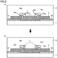
Fig. 2 is a schematic cross sectional view of a graphene transistor according to an embodiment. -
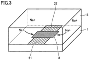
Fig. 3 is a schematic perspective view of the graphene transistor according to the embodiment. -
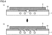
Fig. 4 is a schematic cross sectional view of the graphene transistor according to the embodiment. -
Fig. 5 is a graph showing an IDS-Vg characteristic (relation between a gate voltage and a drain current) of graphene in Examples. -
Fig. 6 is a graph showing a relation between the gate voltage (Vg) and a transconductance (gm) in the Examples. -
Fig. 7 is a graph showing a relation between a time having passed from start of measurement and a Dirac point voltage (VDirac) in the Examples. -
Fig. 8 is a graph showing a relation between the time having passed from the start of measurement and the transconductance (gm) in the Examples. - Hereinafter, embodiments of the present invention will be described with reference to figures. It should be noted that in the figures, the same reference characters represent the same or corresponding portions. Further, dimensional relations such as length, width, thickness, and depth are changed appropriately for the sake of clarity and simplicity of the figures, and do not represent actual dimensional relations.
- Referring to
Fig. 2 , a graphene transistor (graphene field effect transistor: GFET) of the present embodiment includes: agraphene layer 3 composed of at least one sheet of graphene; and adrain electrode 21 and asource electrode 22 each electrically connected tographene layer 3. - The graphene transistor of the present embodiment further includes a charge donor. The charge donor includes impurity charges and is present on at least one main surface of
graphene layer 3. The impurity charges are positive or negative charges. Examples of the impurity charges include a polar molecule (H2O or the like), an ionized functional group (an amino group, a carboxyl group, or the like), a radical, a dangling bond of a covalent material, and an element vacancy in a material (oxygen vacancy in an oxide or the like). - The charge donor is, for example, at least one of
insulative substrate 1 that supportsgraphene layer 3 and an insulativeforeign matter 4. Examples of the insulative foreign matter include a residue of an organic material (PMMA or the like) such as a resist used for patterning ofgraphene layer 3 andelectrodes - A feature of the graphene transistor of the present embodiment lies in that the graphene transistor of the present embodiment further includes counter ions. Each of the counter ions is an ion having a charge having a sign different from a sign of the impurity charge in the charge donor. With the counter ions, the impurity charges in the charge donor can be canceled to reduce the influence of the charge donor upon the graphene layer over time. Thus, changes in characteristics of the graphene layer over time can be suppressed.
- When the impurity charges are negative charges, examples of the counter ions include metal ions, hydrogen ions, or ions having positively chargeable functional groups. Examples of the metal ions include alkali metal ions (sodium ions (Na+) or the like) and alkaline earth metal ions.
- When the impurity charges are positive charges, examples of the counter ions include halogen ions, hydroxide ions, and ions having negatively chargeable functional groups.
- The counter ions are preferably present inside the charge donor or in the vicinity of the charge donor to obtain the effect of canceling the influence of the impurity charges of the charge donor upon the graphene layer. Specifically, the counter ions are preferably included in at least one of inside of the charge donor and an interface between the charge donor and the graphene layer, for example. With the counter ions being present at such a position, the influence of the charge donor upon the graphene layer over time can be reduced more securely.
- It should be noted that the graphene transistor shown in
Fig. 2 includesinsulative substrate 1, andgraphene layer 3,drain electrode 21,source electrode 22, and the like are provided on one main surface ofinsulative substrate 1. However, in the present embodiment, the graphene transistor does not need to includeinsulative substrate 1 necessarily. - The graphene transistor of the present embodiment may further include a gate electrode (not shown) capable of externally applying an electric field to
graphene layer 3. - It should be noted that for example, the main surface of graphene layer 3 (main surface of
graphene layer 3 opposite to the insulative substrate) may be modified with a functional group that can adsorb a detection target or that can bind to the detection target. Further, for example, a receptor (an antibody, an aptamer, or the like) that can bind to the detection target may be bound to the main surface ofgraphene layer 3. It should be noted that the receptor may be bound to the graphene layer via a linker. Thus, the graphene transistor of the present embodiment can be suitably used as a sensor (biosensor or the like) for specifically detecting a detection target. - The thickness of
graphene layer 3 and the number of graphene layer(s) 3 are not particularly limited, but are, for example, 0.3 to 5 nm (1 to 10 layers). The thickness ofinsulative substrate 1 is not particularly limited. - Hereinafter, an exemplary method of manufacturing the graphene transistor according to the present embodiment will be described.
- The manufacturing method of the present embodiment is a method of manufacturing the graphene transistor, the graphene transistor including:
-
graphene layer 3 composed of graphene; and -
drain electrode 21 andsource electrode 22 each electrically connected tographene layer 3; and - the charge donor present on at least one main surface of
graphene layer 3, the charge donor including the impurity charges. - The manufacturing method of the present embodiment includes a counter ion imparting step of imparting counter ions to the graphene transistor, each of the counter ions being an ion having a charge having a sign different from a sign of the impurity charge.
- Examples of a method of imparting the counter ions to the graphene transistor in the counter ion imparting step include, but not particularly limited to, a method of immersing the graphene transistor in an ionic solution including the counter ions. In this way, the counter ions can permeate at least one of the inside of the charge donor and the interface between the charge donor and
graphene layer 3. - Examples of the ionic solution include, but not particularly limited to, a phosphate-buffered saline (PBS), a sodium chloride solution, a potassium chloride solution, a magnesium chloride solution, a sodium hydroxide solution, and the like.
- For example, referring to
Fig. 2 , by immersing the graphene transistor inionic solution 5 including the counter ions (Na+), the counter ions permeate insulative foreign matter 4 (charge donor) including the impurity charges (negative (-) charges) (seeFig. 2 (a) ). Thus, the influence (white arrows in the figure) of the impurity charges of insulative foreign matter 4 (charge donor) upongraphene layer 3 can be considered to be reduced (seeFig. 2 (b) ). - Further, for example, referring to
Fig. 3 , by immersing the graphene transistor inionic solution 5 including the counter ions (Na+), the counter ions permeate the interface between insulative substrate 1 (charge donor) including the impurity charges (negative (-) charges) and graphene layer 3 (seeFig. 3 ). Thus, referring toFig. 4 , the influence (white arrow in the figure) of the impurity charges of insulative substrate 1 (charge donor) upongraphene layer 3 can be considered to be reduced (seeFigs. 4 (a) and 4 (b) ). - An immersion time into the ionic solution is not particularly limited, the immersion time may be any time with which the counter ions can permeate at least one of the inside of the charge donor and the interface between the charge donor and
graphene layer 3 or may be a time longer than that, and the immersion time is preferably more than or equal to 2 hours and is more preferably more than or equal to 10 hours, for example. - It should be noted that in the step of imparting the counter ions, an electric field may be applied between the gate electrode and
graphene layer 3 with the graphene transistor being immersed in the ionic solution. Further, the hydraulic pressure ofionic solution 5 may be increased with the graphene transistor being immersed in the ionic solution. With such an operation, the counter ions are expected to efficiently permeate the charge donor or the like. - Further, the step of imparting the counter ions may be performed by a method other than the method of immersing the graphene transistor in the ionic solution. For example, in the present embodiment, the following step is also encompassed in the step of imparting the counter ions: the counter ions are previously contained in a material (resist material (PMMA or the like) that can serve as insulative
foreign matter 4, or insulative substrate 1) that can serve as the charge donor, and they are used to manufacture a graphene transistor. - The graphene transistor can be manufactured by various known methods. Examples of a method of forming
graphene layer 3 include a method of forming a graphene layer on a copper foil by a chemical vapor deposition (CVD) method and transferring the graphene layer onto an insulative substrate. Further, the method of forminggraphene layer 3 is not limited thereto, and the following method may be used: a method of transferring, onto an insulative substrate, a graphene layer obtained from natural graphite or the like by mechanical removal or the like; a method of forming a graphene layer on an insulative substrate by performing heat treatment onto a SiC substrate (insulative substrate); a method of obtaining a graphene layer by reduction of graphene oxide; or the like. - A graphene transistor (GFET) as shown in
Fig. 1 was produced as Comparative Example 1 by forming a graphene layer on one main surface of a SiO substrate (insulative substrate) by the CVD method and performing patterning (lithography) using PMMA as a resist. - A graphene transistor of Comparative Example 2 was obtained by immersing the same graphene transistor as that of Comparative Example 1 in deionized water for 50 hours.
- A graphene transistor of Example 1 was obtained by immersing the same graphene transistor as that of Comparative Example 1 in 15 mM phosphate-buffered saline (PBS) for 50 hours.
- For each of the graphene transistors of Example 1, Comparative Example 1 and Comparative Example 2, the IDS-Vg characteristic of the graphene layer was measured.
- Specifically, a gate voltage (Vg) [top gate voltage] was applied by the gate electrode having its tip immersed in the PBS with the PBS being present (depth: 5 mm) on the respective surfaces of the graphene layer, the drain electrode, and the source electrode opposite to the insulative substrate. The IDS-Vg characteristic of the graphene was measured by measuring the drain current (IDS) when the gate voltage was changed between -0.1 V and 0.3 V. Measurement results are shown in
Fig. 5 . - As shown in
Fig. 5 , in Example 1 involving the immersion in the PBS, it is understood that VDirac is changed as compared with Comparative Example 1 (white arrow in the figure). It is considered that a component in the PBS affects the characteristic of the graphene layer in view of such a fact that in Comparative Example 2 only involving the immersion in the water, VDirac is hardly changed as compared with Comparative Example 1. - It should be noted that the Dirac point (DP) voltage (VDirac) is a value of Vg at which the value of IDS becomes minimum in the drain current (IDS)-gate voltage (Vg) characteristic as shown in
Fig. 5 . - In a sensor using the graphene transistor, for example, measurement of a detection target can be performed based on an amount of change in Vg when the detection target is attached to the graphene layer, an amount of change in IDS at a specific Vg, or the like.
-
Fig. 6 shows a relation between the gate voltage (Vg) and a transconductance (gm) in the Examples. The transconductance (gm) is the slope (dIDS/dVg) in the IDS-Vg characteristic shown inFig. 5 . The transconductance (gm) is an index representing sensitivity of the drain current with respect to a change in bias voltage between the gate electrode and the source electrode. - As shown in
Fig. 6 , in Example 1, the maximum value of gm is larger than those in Comparative Examples 1 and 2 (white arrow in the figure), and the minimum value of gm is smaller than those in Comparative Examples 1 and 2. As the absolute value of gm is larger, the sensitivity of the measurement in sensing using the graphene transistor is higher, so that it is considered that the sensitivity of the measurement using the graphene transistor of Example 1 is improved as compared with those in Comparative Examples 1 and 2. -
Fig. 5 (andFig. 6 ) show results immediately after starting the above-described measurement of the IDS-Vg characteristic, whereasFig. 7 shows a change in VDirac until 50 minutes passed from the start of the measurement in each of Example 1 and Comparative Example 1, andFig. 8 shows a change in gm until 50 minutes passed from the start of the measurement in each of Example 1 and Comparative Example 1. - As shown in
Fig. 7 , in the graphene transistor of Example 1 having been immersed in the PBS, the change in VDirac over time (white arrow in the figure) is smaller than the change in VDirac over time (black arrow in the figure) in Comparative Example 1. - Further, as shown in
Fig. 8 , it is understood that in the graphene transistor of Example 1 having been immersed in the PBS, the change in VDirac over time (white arrow in the figure) is smaller than the change in VDirac over time (black arrow in the figure) in Comparative Example 1. - In view of the above results, it is understood that by immersing the graphene transistor in the PBS, the changes in characteristics of the graphene layer over time are suppressed.
- This is presumably due to the following reason: since the counter ions (Na+) in the ionic solution (PBS) had permeated at least one of the inside of the charge donor (at least one of the PMMA residue (insulative foreign matter) and the insulative substrate) and the interface between the charge donor and the graphene layer in the initial (pre-use) state, the influence of the impurity charges in the charge donor upon the graphene layer had already been suppressed, thereby avoiding such a phenomenon that the influence of the impurity charges in the charge donor upon the graphene layer is gradually suppressed by the liquid (PBS) used for the measurement.
- The embodiments disclosed herein are illustrative and non-restrictive in any respect. The scope of the present invention is defined by the terms of the claims, rather than the embodiments described above, and is intended to include any modifications within the scope and meaning equivalent to the terms of the claims.
- 1: insulative substrate; 21: drain electrode; 22: source electrode; 3: graphene layer; 4: insulative foreign matter; 5: ionic solution.
Claims (7)
- A graphene transistor comprising:a graphene layer composed of at least one sheet of graphene;a drain electrode and a source electrode each electrically connected to the graphene layer;a charge donor present on at least one main surface of the graphene layer, the charge donor including an impurity charge; anda counter ion, the counter ion being an ion having a charge having a sign different from a sign of the impurity charge.
- The graphene transistor according to claim 1, wherein the counter ion is included in at least one of inside of the charge donor and an interface between the charge donor and the graphene layer.
- The graphene transistor according to claim 1 or 2, wherein the charge donor is at least one of an insulative substrate that supports the graphene layer and an insulative foreign matter.
- The graphene transistor according to any one of claims 1 to 3, comprising an insulative substrate that supports the graphene layer.
- The graphene transistor according to any one of claims 1 to 4, further comprising a gate electrode capable of externally applying an electric field to the graphene layer.
- A method of manufacturing a graphene transistor,the graphene transistor includinga graphene layer composed of graphene,a drain electrode and a source electrode each electrically connected to the graphene layer, anda charge donor present on at least one main surface of the graphene layer, the charge donor including an impurity charge,the method comprising imparting a counter ion to the graphene transistor, the counter ion being an ion having a charge having a sign different from a sign of the impurity charge.
- The method of manufacturing the graphene transistor according to claim 6, wherein in the imparting of the counter ion, the graphene transistor is immersed in an ionic solution including the counter ion.
Applications Claiming Priority (2)
| Application Number | Priority Date | Filing Date | Title |
|---|---|---|---|
| JP2019029080 | 2019-02-21 | ||
| PCT/JP2020/004066 WO2020170799A1 (en) | 2019-02-21 | 2020-02-04 | Graphene transistor and method for manufacturing same |
Publications (2)
| Publication Number | Publication Date |
|---|---|
| EP3905353A1 true EP3905353A1 (en) | 2021-11-03 |
| EP3905353A4 EP3905353A4 (en) | 2022-09-28 |
Family
ID=72143934
Family Applications (1)
| Application Number | Title | Priority Date | Filing Date |
|---|---|---|---|
| EP20758556.3A Withdrawn EP3905353A4 (en) | 2019-02-21 | 2020-02-04 | GRAPHENE-BASED TRANSISTOR AND METHOD FOR MAKING IT |
Country Status (5)
| Country | Link |
|---|---|
| US (1) | US12072313B2 (en) |
| EP (1) | EP3905353A4 (en) |
| JP (1) | JP7178677B2 (en) |
| CN (1) | CN113454799B (en) |
| WO (1) | WO2020170799A1 (en) |
Family Cites Families (18)
| Publication number | Priority date | Publication date | Assignee | Title |
|---|---|---|---|---|
| JP4926855B2 (en) | 2007-06-28 | 2012-05-09 | キヤノン株式会社 | Optical device |
| US8492747B2 (en) * | 2009-10-26 | 2013-07-23 | Samsung Electronics Co., Ltd. | Transistor and flat panel display including thin film transistor |
| KR20120034349A (en) * | 2010-10-01 | 2012-04-12 | 성균관대학교산학협력단 | Flexible field-effect transistor and manufacturing method of the same |
| JP5462219B2 (en) | 2011-05-25 | 2014-04-02 | 株式会社日立製作所 | Graphene sensor, substance species analyzer using the sensor, and substance species detection method using the sensor |
| KR101237351B1 (en) | 2011-05-27 | 2013-03-04 | 포항공과대학교 산학협력단 | Electrode and electronic device comprising the same |
| JP6011620B2 (en) * | 2012-07-13 | 2016-10-19 | 株式会社村田製作所 | Method for manufacturing transistor |
| US9899480B2 (en) * | 2013-03-15 | 2018-02-20 | University Of Notre Dame Du Lac | Single transistor random access memory using ion storage in two-dimensional crystals |
| US9324804B2 (en) * | 2014-03-21 | 2016-04-26 | Wisconsin Alumni Research Foundation | Graphene-on-semiconductor substrates for analog electronics |
| KR102201320B1 (en) * | 2014-06-12 | 2021-01-11 | 삼성전자주식회사 | Semiconductor device, method of manufacturing the same and electronic device including semiconductor device |
| US20180368743A1 (en) * | 2014-06-12 | 2018-12-27 | The Trustees Of Columbia University In The City Of New New York | Graphene-based nanosensor for identifying target analytes |
| JP6374238B2 (en) | 2014-07-01 | 2018-08-15 | クラリオン株式会社 | In-vehicle device |
| KR102360025B1 (en) | 2014-10-16 | 2022-02-08 | 삼성전자주식회사 | Method for forming amorphous carbon monolayer and electronic device having the amorphous carbon monolayer |
| EP3012847B1 (en) * | 2014-10-21 | 2018-02-14 | Nokia Technologies OY | A multilayer graphene composite |
| DE112016004551T5 (en) | 2015-12-24 | 2018-07-12 | Murata Manufacturing Co., Ltd. | SWINGING DEVICE, METHOD FOR CONTROLLING THE SAME AND CAMERA |
| CN106226377A (en) * | 2016-07-06 | 2016-12-14 | 无锡盈芯半导体科技有限公司 | A kind of field-effect transistor biosensor based on Graphene and preparation method thereof |
| JP2018163146A (en) | 2017-03-24 | 2018-10-18 | 株式会社東芝 | Sensor |
| CN110574358B (en) | 2017-04-26 | 2021-05-28 | 株式会社村田制作所 | Cleaning device and imaging unit provided with same |
| CN110999272B (en) | 2017-08-09 | 2021-05-14 | 株式会社村田制作所 | Driving method of vibrating device and vibrating device |
-
2020
- 2020-02-04 WO PCT/JP2020/004066 patent/WO2020170799A1/en not_active Ceased
- 2020-02-04 EP EP20758556.3A patent/EP3905353A4/en not_active Withdrawn
- 2020-02-04 CN CN202080015673.8A patent/CN113454799B/en active Active
- 2020-02-04 JP JP2021501820A patent/JP7178677B2/en active Active
-
2021
- 2021-08-17 US US17/403,915 patent/US12072313B2/en active Active
Also Published As
| Publication number | Publication date |
|---|---|
| JPWO2020170799A1 (en) | 2021-12-02 |
| JP7178677B2 (en) | 2022-11-28 |
| CN113454799B (en) | 2024-08-02 |
| CN113454799A (en) | 2021-09-28 |
| US20210372966A1 (en) | 2021-12-02 |
| WO2020170799A1 (en) | 2020-08-27 |
| EP3905353A4 (en) | 2022-09-28 |
| US12072313B2 (en) | 2024-08-27 |
Similar Documents
| Publication | Publication Date | Title |
|---|---|---|
| Van Ngoc et al. | PMMA-etching-free transfer of wafer-scale chemical vapor deposition two-dimensional atomic crystal by a water soluble polyvinyl alcohol polymer method | |
| Xiao et al. | Room-temperature-processed flexible amorphous InGaZnO thin film transistor | |
| WO2015200758A9 (en) | 3d graphene transistor | |
| US12007354B2 (en) | Rapid detection and identification of bacteria with graphene field effect transistors and peptide probes | |
| Kao et al. | Effects of N2 and O2 annealing on the multianalyte biosensing characteristics of CeO2-based electrolyte–insulator–semiconductor structures | |
| CN104237357A (en) | Sensing element, preparation method and sensor | |
| CN119563107A (en) | Device, hydroxide ion concentration measuring device having the same, and hydroxide ion concentration measuring method using the same | |
| JP5903872B2 (en) | Transistor type sensor and method for manufacturing transistor type sensor | |
| Lin et al. | Comparison between performances of In2O3 and In2TiO5-based EIS biosensors using post plasma CF4 treatment applied in glucose and urea sensing | |
| US8389325B2 (en) | Selective functionalization by joule effect thermal activation | |
| US12072313B2 (en) | Graphene transistor and method of manufacturing same | |
| KR101161371B1 (en) | Field Effect Transistor Biosensor Based on Field Effect Transistor and Method for Fabricating the Same | |
| US9373506B2 (en) | Method for treating surface of diamond thin film, method for forming transistor, and sensor device | |
| Kwon et al. | pH sensing characteristics of extended-gate field-effect transistor with Al2O3 layer | |
| Xu et al. | Development and performance of an all-solid-stated pH sensor based on modified membranes | |
| CN117907405B (en) | Biosensor based on two-dimensional transition metal chalcogenide interface engineering and preparation method thereof | |
| CN121464342A (en) | Device, concentration measuring apparatus provided with the device, and concentration measuring method using the device | |
| Nishimura et al. | Effects of Surface Oxygen Vacancies and Hydroxy Groups on Electrical Characteristics in Solution-Gated One-Piece Indium–Tin-Oxide-Based Field-Effect Transistors | |
| Nascimento et al. | Mechanisms of ion detection for fet-sensors using FTO: Role of cleaning process, ph sequence and electrical resistivity | |
| Huang et al. | High Polarization and Low-Repulsion ${\rm HfO} _ {2} $ Thin Film for Alkali Metal Ion Detections by Plasma System With a Complementary Filter | |
| Narang et al. | Analytical modeling of a split-gate dielectric modulated metal-oxide-semiconductor field-effect transistor for application as a biosensor | |
| CN111416035B (en) | Nonvolatile Hall sensor and manufacturing method and testing method thereof | |
| WO2022102759A1 (en) | Biosensor, method for manufacturing field effect transistor for biosensor, and field effect transistor for biosensor | |
| Baek et al. | Size and surface modification effects on the Ph response of Si nanowire field-effect transistors | |
| Norzin et al. | pH Sensing Characteristics of Silicon Nitride as Sensing Membrane based ISFET Sensor for Artificial Kidney |
Legal Events
| Date | Code | Title | Description |
|---|---|---|---|
| STAA | Information on the status of an ep patent application or granted ep patent |
Free format text: STATUS: THE INTERNATIONAL PUBLICATION HAS BEEN MADE |
|
| PUAI | Public reference made under article 153(3) epc to a published international application that has entered the european phase |
Free format text: ORIGINAL CODE: 0009012 |
|
| STAA | Information on the status of an ep patent application or granted ep patent |
Free format text: STATUS: REQUEST FOR EXAMINATION WAS MADE |
|
| 17P | Request for examination filed |
Effective date: 20210729 |
|
| AK | Designated contracting states |
Kind code of ref document: A1 Designated state(s): AL AT BE BG CH CY CZ DE DK EE ES FI FR GB GR HR HU IE IS IT LI LT LU LV MC MK MT NL NO PL PT RO RS SE SI SK SM TR |
|
| DAV | Request for validation of the european patent (deleted) | ||
| DAX | Request for extension of the european patent (deleted) | ||
| A4 | Supplementary search report drawn up and despatched |
Effective date: 20220830 |
|
| RIC1 | Information provided on ipc code assigned before grant |
Ipc: H01L 51/40 20060101ALI20220824BHEP Ipc: H01L 51/05 20060101ALI20220824BHEP Ipc: H01L 29/786 20060101ALI20220824BHEP Ipc: H01L 29/66 20060101ALI20220824BHEP Ipc: H01L 29/16 20060101ALI20220824BHEP Ipc: G01N 27/414 20060101ALI20220824BHEP Ipc: H01L 51/30 20060101AFI20220824BHEP |
|
| STAA | Information on the status of an ep patent application or granted ep patent |
Free format text: STATUS: EXAMINATION IS IN PROGRESS |
|
| 17Q | First examination report despatched |
Effective date: 20230426 |
|
| STAA | Information on the status of an ep patent application or granted ep patent |
Free format text: STATUS: THE APPLICATION IS DEEMED TO BE WITHDRAWN |
|
| 18D | Application deemed to be withdrawn |
Effective date: 20250225 |