EP3905336A2 - Group iii nitride device and method of fabricating a group iii nitride-based device - Google Patents
Group iii nitride device and method of fabricating a group iii nitride-based device Download PDFInfo
- Publication number
- EP3905336A2 EP3905336A2 EP20199461.3A EP20199461A EP3905336A2 EP 3905336 A2 EP3905336 A2 EP 3905336A2 EP 20199461 A EP20199461 A EP 20199461A EP 3905336 A2 EP3905336 A2 EP 3905336A2
- Authority
- EP
- European Patent Office
- Prior art keywords
- layer
- field plate
- passivation layer
- ohmic contact
- gate
- Prior art date
- Legal status (The legal status is an assumption and is not a legal conclusion. Google has not performed a legal analysis and makes no representation as to the accuracy of the status listed.)
- Pending
Links
Images







Classifications
-
- H—ELECTRICITY
- H10—SEMICONDUCTOR DEVICES; ELECTRIC SOLID-STATE DEVICES NOT OTHERWISE PROVIDED FOR
- H10D—INORGANIC ELECTRIC SEMICONDUCTOR DEVICES
- H10D30/00—Field-effect transistors [FET]
- H10D30/01—Manufacture or treatment
- H10D30/015—Manufacture or treatment of FETs having heterojunction interface channels or heterojunction gate electrodes, e.g. HEMT
-
- H—ELECTRICITY
- H10—SEMICONDUCTOR DEVICES; ELECTRIC SOLID-STATE DEVICES NOT OTHERWISE PROVIDED FOR
- H10D—INORGANIC ELECTRIC SEMICONDUCTOR DEVICES
- H10D64/00—Electrodes of devices having potential barriers
- H10D64/111—Field plates
-
- H—ELECTRICITY
- H10—SEMICONDUCTOR DEVICES; ELECTRIC SOLID-STATE DEVICES NOT OTHERWISE PROVIDED FOR
- H10D—INORGANIC ELECTRIC SEMICONDUCTOR DEVICES
- H10D30/00—Field-effect transistors [FET]
- H10D30/40—FETs having zero-dimensional [0D], one-dimensional [1D] or two-dimensional [2D] charge carrier gas channels
- H10D30/47—FETs having zero-dimensional [0D], one-dimensional [1D] or two-dimensional [2D] charge carrier gas channels having two-dimensional [2D] charge carrier gas channels, e.g. nanoribbon FETs or high electron mobility transistors [HEMT]
- H10D30/471—High electron mobility transistors [HEMT] or high hole mobility transistors [HHMT]
- H10D30/475—High electron mobility transistors [HEMT] or high hole mobility transistors [HHMT] having wider bandgap layer formed on top of lower bandgap active layer, e.g. undoped barrier HEMTs such as i-AlGaN/GaN HEMTs
-
- H—ELECTRICITY
- H10—SEMICONDUCTOR DEVICES; ELECTRIC SOLID-STATE DEVICES NOT OTHERWISE PROVIDED FOR
- H10D—INORGANIC ELECTRIC SEMICONDUCTOR DEVICES
- H10D30/00—Field-effect transistors [FET]
- H10D30/40—FETs having zero-dimensional [0D], one-dimensional [1D] or two-dimensional [2D] charge carrier gas channels
- H10D30/47—FETs having zero-dimensional [0D], one-dimensional [1D] or two-dimensional [2D] charge carrier gas channels having two-dimensional [2D] charge carrier gas channels, e.g. nanoribbon FETs or high electron mobility transistors [HEMT]
- H10D30/471—High electron mobility transistors [HEMT] or high hole mobility transistors [HHMT]
- H10D30/475—High electron mobility transistors [HEMT] or high hole mobility transistors [HHMT] having wider bandgap layer formed on top of lower bandgap active layer, e.g. undoped barrier HEMTs such as i-AlGaN/GaN HEMTs
- H10D30/4755—High electron mobility transistors [HEMT] or high hole mobility transistors [HHMT] having wider bandgap layer formed on top of lower bandgap active layer, e.g. undoped barrier HEMTs such as i-AlGaN/GaN HEMTs having wide bandgap charge-carrier supplying layers, e.g. modulation doped HEMTs such as n-AlGaAs/GaAs HEMTs
-
- H—ELECTRICITY
- H10—SEMICONDUCTOR DEVICES; ELECTRIC SOLID-STATE DEVICES NOT OTHERWISE PROVIDED FOR
- H10D—INORGANIC ELECTRIC SEMICONDUCTOR DEVICES
- H10D62/00—Semiconductor bodies, or regions thereof, of devices having potential barriers
- H10D62/80—Semiconductor bodies, or regions thereof, of devices having potential barriers characterised by the materials
- H10D62/82—Heterojunctions
- H10D62/824—Heterojunctions comprising only Group III-V materials heterojunctions, e.g. GaN/AlGaN heterojunctions
-
- H—ELECTRICITY
- H10—SEMICONDUCTOR DEVICES; ELECTRIC SOLID-STATE DEVICES NOT OTHERWISE PROVIDED FOR
- H10D—INORGANIC ELECTRIC SEMICONDUCTOR DEVICES
- H10D64/00—Electrodes of devices having potential barriers
- H10D64/01—Manufacture or treatment
-
- H—ELECTRICITY
- H10—SEMICONDUCTOR DEVICES; ELECTRIC SOLID-STATE DEVICES NOT OTHERWISE PROVIDED FOR
- H10D—INORGANIC ELECTRIC SEMICONDUCTOR DEVICES
- H10D64/00—Electrodes of devices having potential barriers
- H10D64/111—Field plates
- H10D64/117—Recessed field plates, e.g. trench field plates or buried field plates
-
- H—ELECTRICITY
- H10—SEMICONDUCTOR DEVICES; ELECTRIC SOLID-STATE DEVICES NOT OTHERWISE PROVIDED FOR
- H10D—INORGANIC ELECTRIC SEMICONDUCTOR DEVICES
- H10D64/00—Electrodes of devices having potential barriers
- H10D64/20—Electrodes characterised by their shapes, relative sizes or dispositions
- H10D64/23—Electrodes carrying the current to be rectified, amplified, oscillated or switched, e.g. sources, drains, anodes or cathodes
- H10D64/251—Source or drain electrodes for field-effect devices
-
- H—ELECTRICITY
- H10—SEMICONDUCTOR DEVICES; ELECTRIC SOLID-STATE DEVICES NOT OTHERWISE PROVIDED FOR
- H10D—INORGANIC ELECTRIC SEMICONDUCTOR DEVICES
- H10D64/00—Electrodes of devices having potential barriers
- H10D64/20—Electrodes characterised by their shapes, relative sizes or dispositions
- H10D64/27—Electrodes not carrying the current to be rectified, amplified, oscillated or switched, e.g. gates
- H10D64/311—Gate electrodes for field-effect devices
- H10D64/411—Gate electrodes for field-effect devices for FETs
-
- H—ELECTRICITY
- H10—SEMICONDUCTOR DEVICES; ELECTRIC SOLID-STATE DEVICES NOT OTHERWISE PROVIDED FOR
- H10W—GENERIC PACKAGES, INTERCONNECTIONS, CONNECTORS OR OTHER CONSTRUCTIONAL DETAILS OF DEVICES COVERED BY CLASS H10
- H10W10/00—Isolation regions in semiconductor bodies between components of integrated devices
- H10W10/01—Manufacture or treatment
- H10W10/051—Manufacture or treatment of isolation region based on field-effect
-
- H—ELECTRICITY
- H10—SEMICONDUCTOR DEVICES; ELECTRIC SOLID-STATE DEVICES NOT OTHERWISE PROVIDED FOR
- H10W—GENERIC PACKAGES, INTERCONNECTIONS, CONNECTORS OR OTHER CONSTRUCTIONAL DETAILS OF DEVICES COVERED BY CLASS H10
- H10W10/00—Isolation regions in semiconductor bodies between components of integrated devices
- H10W10/50—Isolation regions based on field-effect
-
- H—ELECTRICITY
- H10—SEMICONDUCTOR DEVICES; ELECTRIC SOLID-STATE DEVICES NOT OTHERWISE PROVIDED FOR
- H10W—GENERIC PACKAGES, INTERCONNECTIONS, CONNECTORS OR OTHER CONSTRUCTIONAL DETAILS OF DEVICES COVERED BY CLASS H10
- H10W74/00—Encapsulations, e.g. protective coatings
- H10W74/10—Encapsulations, e.g. protective coatings characterised by their shape or disposition
- H10W74/131—Encapsulations, e.g. protective coatings characterised by their shape or disposition the semiconductor body being only partially enclosed
- H10W74/137—Encapsulations, e.g. protective coatings characterised by their shape or disposition the semiconductor body being only partially enclosed the encapsulations being directly on the semiconductor body
-
- H—ELECTRICITY
- H10—SEMICONDUCTOR DEVICES; ELECTRIC SOLID-STATE DEVICES NOT OTHERWISE PROVIDED FOR
- H10W—GENERIC PACKAGES, INTERCONNECTIONS, CONNECTORS OR OTHER CONSTRUCTIONAL DETAILS OF DEVICES COVERED BY CLASS H10
- H10W74/00—Encapsulations, e.g. protective coatings
- H10W74/40—Encapsulations, e.g. protective coatings characterised by their materials
- H10W74/43—Encapsulations, e.g. protective coatings characterised by their materials comprising oxides, nitrides or carbides, e.g. ceramics or glasses
-
- H—ELECTRICITY
- H10—SEMICONDUCTOR DEVICES; ELECTRIC SOLID-STATE DEVICES NOT OTHERWISE PROVIDED FOR
- H10D—INORGANIC ELECTRIC SEMICONDUCTOR DEVICES
- H10D62/00—Semiconductor bodies, or regions thereof, of devices having potential barriers
- H10D62/80—Semiconductor bodies, or regions thereof, of devices having potential barriers characterised by the materials
- H10D62/85—Semiconductor bodies, or regions thereof, of devices having potential barriers characterised by the materials being Group III-V materials, e.g. GaAs
- H10D62/8503—Nitride Group III-V materials, e.g. AlN or GaN
Definitions
- transistors used in power electronic applications have typically been fabricated with silicon (Si) semiconductor materials.
- Common transistor devices for power applications include Si CoolMOS®, Si Power MOSFETs, and Si Insulated Gate Bipolar Transistors (IGBTs).
- SiC silicon carbide
- Group III-N semiconductor devices such as gallium nitride (GaN) devices, are now emerging as attractive candidates to carry large currents, support high voltages and to provide very low on-resistance and fast switching times. Further improvements to Group III nitride-based devices, are, however desirable.
- a method of fabricating a Group III nitride-based transistor comprises providing a substrate comprising a Group III nitride-based layer, a first passivation layer on the first major surface of the Group III nitride-based layer and a second passivation layer arranged on the first passivation layer, the second passivation layer having a different composition from the first passivation layer, forming a first mask layer on the second passivation layer, the first mask layer comprising a first insulating layer arranged on the second passivation layer and a first resist layer on the first insulating layer, forming a first opening for a gate electrode in the first mask layer, the first opening extending through the first resist layer and through the first insulating layer, forming a second opening for a field plate in the first mask layer, the second opening extending through the first resist layer and through the first insulating layer, removing the second passivation layer exposed by the first opening and forming a first via for the gate electrode, the first via
- the first resist layer is a photoresist layer and the second resist layer is a photoresist layer.
- the electrically conductive layer is a tungsten layer.
- the method further comprises depositing the tungsten layer onto the second passivation layer laterally adjacent to the first via and the second via, and planarising to form a planarised surface comprising isolated areas of tungsten surrounded by the second passivation layer.
- the second resist layer leaves a portion of the first insulating layer that is arranged adjacent the first via exposed.
- the first insulating layer and the first photoresist are patterned using DUV (deep ultra violet) technology.
- the base of the first via has a width 30 nm to 500 nm, for example a width of around 250 nm or less or of 225nm to 350 nm, for example around 250nm and/or a minimum distance between the base of the first via and the second via is at the closest point 30 nm to 500nm, or 225nm to 350 nm, for example 250nm or less.
- a base of the first via and a base of the second via each have a width of 50 nm to 400 nm, or 200nm to 350 nm, for example around 250nm and the distance between the first and second at the closest point is 100 nm to 400 nm, or 200nm to 350 nm, for example around 250nm.
- the first passivation layer comprises silicon nitride
- the second passivation layer comprises silicon oxide
- the first insulating layer comprises titanium nitride
- the substrate further comprises a first ohmic contact and a second ohmic contact on the first major surface of the Group III nitride-based layer
- the first passivation layer is located on the first major surface of the Group III nitride-based layer and extends between the first ohmic contact and the second ohmic contact
- the second passivation layer is arranged on the first passivation layer and on the first ohmic contact and on the second ohmic contact.
- the substrate comprises a first passivation layer arranged on the first major surface.
- the method further comprises forming the first ohmic contact and the second ohmic contact on the first major surface of the Group III nitride-based layer that extend at least partially through the first passivation layer, covering the first ohmic contact and the second ohmic contact with a first sublayer of passivation material, planarising to form an intermediate planarized surface comprising a surface of the first ohmic contact, a surface of the second ohmic contact and the first sublayer, and forming a second sublayer of passivation material on the planarized surface and arranged on the first ohmic contact and the second ohmic contact, the first and second sublayers forming the second passivation layer.
- the method further comprises forming a structure for a second ohmic contact.
- the second ohmic contact may be a drain contact and the first ohmic contact may be a source contact.
- the structure for the first and second ohmic contacts may be formed using the same process, for example the same mask layers.
- the structure for the first and second ohmic contacts may be formed using the same process, for example the same mask layers, as for the gate and field plate(s).
- the method further comprises forming a third opening in the first mask layer, the third opening extending through the first photoresist layer and the first insulating layer and being positioned above the second ohmic contact, removing the second passivation layer exposed in the third opening and forming a third via having a base exposing a portion of the second ohmic contact, covering the third via with the second resist layer, and after removal of the second resist layer further depositing the tungsten into the third via, and planarising to form a planarised surface comprising isolated areas of tungsten positioned in the first, second and third vias, each isolated area of tungsten being surrounded by the second passivation layer.
- a second conductive layer of the metallization structure is fabricated.
- the method further comprises forming a second insulation layer on the second passivation layer and on the isolated areas of tungsten, forming a third insulating layer on the second insulation layer, the second and third insulation layers having differing compositions, structuring the third insulation layer to form a first trench positioned above the first via, the first trench having a base spaced apart from the first via by a portion of the third insulating layer and the second insulating layer, the first trench being laterally wider than the first via, forming a fourth via in the base of the first trench that exposes the tungsten in the first via by removing the third insulation layer and the second insulation layer, the fourth via being laterally smaller than the first trench and forming a second tungsten layer in the fourth via and in the first trench.
- trenches and vias for the gate and the field plate are formed in the second conductive level of metallization structure.
- the method further comprises structuring the third insulation layer to form a second trench above the second via and a third trench above the third via, the second trench having a base spaced apart from the second via by a portion of the third insulating layer and the second insulating layer, the second trench being laterally wider than the second via, the third trench having a base spaced apart from the third via by a portion of the third insulating layer and the second insulating layer, the third trench being laterally wider than the third via, forming a fifth via in the second trench that exposes the tungsten in the second via by removing the third insulation layer in the base of the second trench, forming a sixth via in the third trench that exposes the tungsten in the third via by removing the third insulation layer in the base of the third trench, and depositing the second tungsten layer into the second and third trenches and into the fifth and sixth vias.
- a Group III nitride-based transistor device comprises a source electrode, a drain electrode and a gate electrode positioned on a first major surface of a Group III nitride based-based layer, wherein the gate is laterally arranged between the source electrode and the drain electrode, and a field plate, the field plate being laterally arranged between and spaced apart from the gate electrode and the drain electrode.
- a base of the gate electrode and a base of the field plate each have a width of 50 nm to 400 nm, or 200nm to 350 nm, for example around 250nm and the distance between the gate electrode and the field plate at the closest point is 100 nm to 400 nm, or 200nm to 350 nm, for example around 250nm.
- a Group III nitride-based transistor device comprises a first passivation layer arranged on a first major surface of a Group III nitride based-based layer, a second passivation layer arranged on the first passivation layer, a source ohmic contact, a drain ohmic contact and a gate positioned on the first major surface of a Group III nitride based-based layer, wherein the gate is laterally arranged between the source ohmic contact and the drain ohmic contact and comprises a gate via extending to an upper surface of the second passivation layer, a field plate, the field plate being laterally arranged between and spaced apart from the gate and the drain ohmic contact and extending to an upper surface of the second passivation layer, a first via extending from the source ohmic contact to an upper surface of the second passivation layer, a second via extending from the drain ohmic contact to the upper surface of the second passivation layer,
- the source ohmic contact comprises a base portion having a conductive surface, the conductive surface comprising a peripheral portion and a central portion, the peripheral portion and the central portion being substantially coplanar and being of differing composition.
- the first via is positioned on the central portion of the conductive surface.
- the drain ohmic contact comprises a base portion having a conductive surface, the conductive surface comprising a peripheral portion and a central portion, the peripheral portion and the central portion being substantially coplanar and being of differing composition.
- the second via is positioned on the central portion of the conductive surface.
- the central portion comprises TiN and the peripheral portion comprises aluminium or an aluminium copper or a titanium aluminium alloy.
- a base of the field plate is in direct contact with the first passivation layer
- a base of the gate via is in direct contact with the first major surface
- the source ohmic contact extends at least partially through the first passivation layer
- the drain ohmic contact extends at least partially through the first passivation layer.
- the field plate extends substantially perpendicular to the first major surface and is electrically coupled to the source electrode by a lateral field plate redistribution structure that extends over and is spaced apart from the gate electrode.
- the source electrode, the gate electrode, the drain electrode and the field plate each have an elongate form and extend on the first major surface in a longitudinal direction substantially parallel to one another.
- the lateral field plate redistribution structure comprises a longitudinal section positioned above the field plate and extending substantially parallel to the longitudinal direction and a plurality of transverse sections spaced at intervals in the longitudinal direction, each transverse section extending over and being spaced apart from the gate electrode and being electrically coupled to the field plate by a field plate conductive via.
- the Group III nitride-based transistor device further comprises a lateral gate redistribution structure, the lateral gate distribution structure comprising a plurality of transverse sections that extend substantially perpendicularly to the longitudinal direction, each transverse section being spaced apart from the gate electrode and electrically coupled to the gate electrode by a gate conductive via, the transverse section of the lateral gate distribution structure being interleaved with the transverse sections of the lateral field plate distribution structure.
- the source electrode is electrically coupled to the lateral field plate redistribution structure.
- the Group III nitride-based transistor device further comprises a source redistribution structure, wherein the source electrode is electrically coupled by one or more source conductive vias to the source redistribution structure and the source redistribution structure is integral with the transverse sections of the field plate redistribution structure.
- the source redistribution structure is formed of the source conductive vias and includes no lateral redistribution structure in the plane of the field plate redistribution structure.
- the source redistribution structure includes a longitudinal section extending in the longitudinal direction and arranged above and spaced apart from the source electrode.
- the longitudinal section of the source redistribution structure may be substantially coplanar with the longitudinal and transverse sections of the lateral field plate redistribution structure.
- the longitudinal section of the source redistribution structure may also be substantially coplanar with the later gate redistribution structure.
- the longitudinal section of the lateral field plate redistribution structure is laterally wider than the field plate.
- the field plate is spilt into two field plate sections that extend substantially parallel to one another and are laterally spaced apart from one another, the two field plate sections being laterally arranged between and spaced apart from the gate electrode and the drain electrode.
- a Group III nitride-based transistor device comprising a source electrode, a drain electrode and a gate electrode positioned on a first major surface of a Group III nitride based-based layer, wherein the gate is laterally arranged between the source electrode and the drain electrode, a passivation layer arranged on the first major surface and a field plate coupled to the source electrode.
- the field plate has a lower surface arranged on the passivation layer and is laterally arranged between and laterally spaced apart from the gate electrode and the drain electrode.
- the source electrode, the gate electrode, the drain electrode and the field plate each have an elongate form and extend on the first major surface in a longitudinal direction substantially parallel to one another.
- the Group III nitride-based transistor device further comprises a conductive redistribution structure that is arranged above the source electrode, the gate electrode, the drain electrode and the field plate and comprises a lateral gate redistribution structure and a lateral field plate redistribution structure that are substantially coplanar at a position laterally between the source electrode and the drain electrode.
- the lateral gate redistribution structure and the lateral field plate redistribution structure are arranged in a plane above the plane of the gate electrode and the field plate.
- the lateral gate redistribution structure and the lateral field plate redistribution structure are positioned at least partially above the active region of the Group III nitride-based transistor device since they are arranged laterally between the source electrode and drain electrode.
- an upper surface of the field plate and an upper surface of the gate electrode are substantially coplanar.
- the gate electrode is electrically coupled to the lateral gate redistribution structure by one or more gate conductive vias.
- the one or more gate conductive vias are positioned laterally between the source electrode and the gate electrode in order to electrically connect the gate electrode to the lateral gate redistribution structure.
- the one or more gate conductive vias are arranged above the active region of the Group III nitride-based transistor device.
- the field plate is electrically coupled to the lateral field plate redistribution structure by one or more field plate conductive vias.
- the one or more field plate conductive vias are positioned laterally between the source electrode and the drain electrode in order to electrically connect field plate to the lateral field plate redistribution structure.
- the one or more field plate conductive vias are arranged above the active region of the Group III nitride-based transistor device.
- an upper surface of the source electrode and an upper surface of the drain electrode are substantially coplanar and arranged at a distance above the first major surface that is less than the distance between the upper surface of the gate electrode and the first major surface. This arrangement allows the source and drain electrode to be fabricated before the gate electrode and field plate.
- the source electrode is electrically coupled to the lateral field plate redistribution structure by one or more source conductive vias.
- the field plate is coupled to source potential in these embodiments.
- the lateral field plate redistribution structure extends over and is spaced apart from the gate electrode. This enables the lateral field plate redistribution structure to act as a shield for the gate electrode that is positioned underneath and spaced at a distance from the lateral field plate redistribution structure.
- the lateral field plate redistribution structure comprises a plurality of transverse sections spaced at intervals in the longitudinal direction, each transverse section extending over and being spaced apart from the gate electrode and being electrically coupled to the field plate by a field plate conductive via.
- the transverse sections together cover less than 50% or less than 20% of a length of the gate electrode. This arrangement may be described as a partially shielded structure.
- the transverse sections together cover at least 50% or at least 80% of a length of the gate electrode. This arrangement may be described as a shielded or fully shielded structure.
- the transverse sections of the lateral field plate structure are arranged above and spaced apart from the source electrode and the source electrode is electrically coupled by one or more source conductive vias to the transverse sections of the field plate redistribution structure.
- the source conductive vias and the field plate conductive vias are arranged adjacent and spaced apart from opposing sides of the gate electrode.
- the lateral field plate redistribution structure further comprises a longitudinal section positioned above the field plate and extending substantially parallel to the longitudinal direction and to the field plate, wherein the longitudinal section is connected to the transverse sections. This arrangement may be used to increase the fielding of the gate electrode.
- the longitudinal section of the lateral field plate redistribution structure is laterally wider than the conductive vias and the field plate. This arrangement may be used to further increase the fielding of the gate electrode.
- the field plate is spilt into two field plate sections that extend substantially parallel to one another and are laterally spaced apart from one another, the two field plate sections being laterally arranged between and spaced apart from the gate electrode and the drain electrode.
- the lateral gate distribution structure comprises a plurality of transverse sections spaced at intervals in the longitudinal direction, each transverse section being spaced apart from the gate electrode and electrically coupled to the gate electrode by a gate conductive via.
- the transverse sections of the lateral gate redistribution structure are interleaved with the transverse sections of the lateral field plate distribution structure.
- an upper surface of the lateral gate redistribution structure is substantially coplanar with an upper surface of the lateral field plate distribution structure.
- the transverse sections of the lateral gate redistribution structure extend over and are spaced apart from the source electrode.
- the lateral gate redistribution structure further comprises a longitudinal section that is positioned on an opposing side of the source electrode from the gate electrode and the transverse sections of the lateral gate redistribution structure are connected to the longitudinal section.
- the lateral gate redistribution structure may also provide the gate pad with the lateral redistribution from the gate pad to the gate electrode being and substantially coplanar with the lateral field plate and drain redistribution structures.
- the vertical connection between the gat electrode and the lateral gate redistribution structure of the upper level is arranged directly above the gate electrode, i.e. by the one or more gate conductive vias extending between the gate electrode and the lateral gate redistribution structure, in the active area of the Group III nitride transistor device at a position laterally between the source and drain electrodes.
- lateral or lateral direction should be understood to mean a direction or extent that runs generally parallel to the lateral extent of a semiconductor material or semiconductor carrier.
- the lateral direction thus extends generally parallel to these surfaces or sides.
- vertical or “vertical direction” is understood to mean a direction that runs generally perpendicular to these surfaces or sides and thus to the lateral direction. The vertical direction therefore runs in the thickness direction of the semiconductor material or semiconductor carrier.
- Group III-Nitride refers to a compound semiconductor that includes nitrogen (N) and at least one Group III element, including aluminum (Al), gallium (Ga), indium (In), and boron (B), and including but not limited to any of its alloys, such as aluminum gallium nitride (Al x Ga (1-x) N), indium gallium nitride (In y Ga (1-y) N), aluminum indium gallium nitride (Al x In y Ga (1-x-y) N), gallium arsenide phosphide nitride (GaAs a P b N (1-a-b) ), and aluminum indium gallium arsenide phosphide nitride (Al x In y Ga (1-x-y) As a PbN (1-a-b) ), for example.
- Aluminum gallium nitride and AlGaN refers to an alloy described by the formula Al x Ga
- Methods for fabricating an ohmic contact for Group III nitride-based devices are used that enable the fabrication of a device with a short gate length Lg, for example Lg ⁇ 250 nm, and an optimized feed-back capacitance Cgd.
- Such short gate lengths are useful for radio-frequency application transistors requiring a high transition frequency fT in the range 50 GHz to 150 GHz.
- Such short gate lengths can be achieved using high precision patterning for which photolithography processes with thin photo resist flows are required.
- This disclosure makes use of an ohmic metallization concept which leaves no topography steps such as vertical steps due to RIE (Reactive Ion Etching) patterning of the Ohmic metal stack for the source and drain contacts so that photolithography can be applied to form shorter gate lengths and to position the gate more closely to the source contact to reduce R DSON .
- the methods can be carried out using the process capabilities of a 200 mm CMOS production line and, therefore, cost effectively on wafers having a diameter of at least 200 mm.
- an Ohmic contact-first approach is used to fabricate a Group III nitride-based device, in particular a transistor device such as a HEMT (High Electron Mobility Transistor).
- the method is carried out on a wafer, which may have a diameter of 6 inches or more, and includes planarizing the Ohmic metal before the fabrication of the gate structure.
- the ohmic metal may be formed by opening a window in the Group III nitride passivation, depositing an Ohmic metal stack, structuring the Ohmic metal stack and applying the Ohmic metal anneal step to alloy the ohmic metal.
- the ohmic metal can be planarized by depositing a CMP (Chemical Mechanical Polishing) stop layer on the frontside of the wafer, using chemical mechanical polishing on the structured Ohmic metal to produce a planarized surface and afterwards stripping the remaining parts of the stop layer.
- CMP Chemical Mechanical Polishing
- planarized surface is used for the further processing of the device, for example to form the gate using photolithography without underlying topography affecting the accuracy of the photolithographic process.
- Advantages of this approach include enabling of a low gate to source distance to enhance device performance and improving the critical dimension control of the gate process to enhance manufacturability and device performance.
- FIG. 1 illustrates a schematic cross-sectional view of a Group III nitride-based device 10 according to an embodiment.
- the Group III nitride-based device 10 includes a Group III nitride-based layer 11, a first ohmic contact 12, a second ohmic contact 13 and a gate 14, which are arranged on a first major surface 15 of the Group III nitride-based layer 11.
- the Group III nitride-based device 10 may be a transistor device 16 such as a High Electron Mobility Transistor (HEMT).
- HEMT High Electron Mobility Transistor
- the first ohmic contact 12 may provide a source contact
- the second ohmic contact 13 may provide a drain contact.
- HEMT High Electron Mobility Transistor
- the gate 14 is arranged laterally between the source contact 12 and the drain contact 13.
- the Group III nitride-based device 10 also includes a field plate 17 that is positioned on the first major surface 15 and laterally between and spaced apart from the gate 14 and the drain contact 13.
- the Group III nitride-based device 10 includes a first passivation layer 18 arranged on the first major surface 15 of the Group III nitride-based layer 11 and a second passivation layer 19 arranged on the first passivation layer 18.
- the source contact 12, the gate 14 and the drain contact 15 extend through the first passivation layer 18, whereas the field plate 17 is arranged on the first passivation layer 18 and spaced apart from the underlying Group III nitride-based layer 11 by the first passivation layer 18.
- the source contact 12, the gate 14 and the drain contact 15 are in direct contact with the Group III nitride-based layer 11.
- Each of the first and second ohmic contacts 12, 13 comprises a base portion 20 having an upper conductive surface 21 that is positioned within the second passivation layer 19.
- Each of the ohmic contacts 12, 13 may have the same structure.
- the ohmic contacts 12, 13 may be fabricated at substantially the same time and are fabricated before the fabrication of the gate 14 and the field plate 17.
- the gate 14 and the field plate 17 are each formed of conductive material and extend through the entire thickness of the second passivation layer 19.
- the gate 14 includes a gate via and the field plate 17 includes a field plate via.
- the gate 14 may be a Schottky contact.
- the transistor device 16 includes an insulated gate contact.
- the first and second ohmic contacts 12, 13 each further comprise a conductive via 22, 23 that is positioned on the conductive surface 21 and that extends through the second passivation layer 19 to the upper surface.
- the conductive surface 21 has a peripheral portion 24 and central portion 25 that are substantially coplanar and are of differing composition.
- the conductive via 22, 23 is positioned on the central portion 25 and has a lateral extent which is less than the lateral extent of the base portion 20. In some embodiments, the lateral extent of the conductive via 22, 23 is less than the lateral extent of the central portion 25 of the conductive surface 21.
- the Group III nitride-based layer 11 may include a multilayer Group III nitride structure positioned on a support substrate 27 which has a growth surface 28 which is capable of supporting the epitaxial growth of at least one Group III nitride layer.
- the support substrate 27 may be monocrystalline silicon substrate, for example a ⁇ 111> or ⁇ 110> silicon wafer or a monocrystalline sapphire substrate.
- the multilayer Group III nitride structure 11 may include a Group III nitride buffer structure 29 arranged on the growth surface 28, a Group III nitride channel layer 30 arranged on the Group III nitride buffer structure 29 and a Group III nitride barrier layer 31 arranged on the Group III nitride channel layer 30.
- the Group III nitride barrier layer 31 has a different composition and bandgap to the Group III nitride channel layer 30 such that a heterojunction 32 is formed therebetween.
- the Group III nitride channel layer 30 may comprise gallium nitride and the Group III nitride barrier layer 31 may comprise aluminium gallium nitride.
- the heterojunction 32 is capable supporting a two-dimensional charge gas which is indicated schematically in the in figure 1 by the dashed line 33.
- the first ohmic contact 12 and the second ohmic contact 13 form an ohmic contact with the two-dimensional charge gas 33.
- a typical buffer structure 29 for a silicon substrate includes a AlN starting layer, which may have a thickness of several 100nm, on the silicon substrate followed by a Al x Ga (1-x) N layer sequence, the thickness again being several 100nm's for each layer, whereby the Al content of about 50-75% is decreased down to 10-25% before the GaN layer of AlGaN back barrier is grown.
- a superlattice buffer can be used. Again, an AlN starting layer on the silicon substrate is used. Depending on the chosen superlattice, a sequence of AlN and Al x Ga (1-x) N pairs is grown, where the thickness of the AlN layer and Al x Ga (1-x) N is in the range of 2-25nm. Depending on the desired breakdown voltage the superlattice may include between 20 and 100 pairs. Alternatively, an Al x Ga (1-x) N layer sequence as described above can be used in combination with the above mentioned superlattice.
- the second passivation layer 19 includes two sublayers.
- the lower sublayer 36 is positioned on the Group III nitride-based barrier layer 30 and, during manufacture of the Group III nitride-based device 10, forms a planar surface with the conductive surface 21 of the base portion 20 of the first and second ohmic contacts 12, 13 before the deposition of the upper sublayer 37 onto the planar surface.
- the lower and upper sublayers 36, 37 may have the same composition, for example silicon oxide, and may be formed using a TEOS (Tetraethyl orthosilicate) process.
- TEOS Tetraethyl orthosilicate
- the first passivation layer 18 is positioned between the upper surface of the Group III nitride-based barrier layer 30 and has a different composition to the second passivation layer 19.
- the first passivation layer 18 may be formed of silicon nitride.
- the passivation layer 18 is formed of a so called "high-k" dielectric, which has a higher dielectric constant compared to silicon dioxide, for example a hafnium- or zirconium-based dielectric materials such as hafnium silicate, hafnium dioxide, zirconium silicate and zirconium dioxide.
- a hafnium- or zirconium-based dielectric materials such as hafnium silicate, hafnium dioxide, zirconium silicate and zirconium dioxide.
- this planarised surface 35 enables the subsequent layers built up upon it to be planar.
- This method enables the photoresist layer for the gate 14 and field plate 17 to be more accurately structured, since it is formed on a planar surface 35 and can be formed after the ohmic contacts 22, 23 are formed to the multilayer Group III structure 11, which typically involves higher processing temperatures.
- the dimensions and position of the gate 14 and field plate 17 can be more accurately controlled.
- This also enables the distance d SG between the ohmic source contact 12 and the gate 14, as measured at the base of the ohmic contact 12 and gate 14, to be reduced and to be reliably produced at this reduced length.
- the gate to source distance d SG may be less than 0,5 ⁇ m, for example 250nm or less in order to lower RDSON and enhance device performance.
- the more accurate structuring of the photoresist layer, the position of the field plate 17 with respect to the gate, d GPP can also be more reliably controlled and may also be less than 0,5 ⁇ m, for example 250nm or less.
- the gate length L G and/or the length of the field plate L FP may also be less than 0,5 ⁇ m, for example 250nm or less.
- This high precision patterning of the gate electrode is enabled as the photoresist processes of the gate and field plate are not affected by topography steps created by the Ohmic metal contacts 12, 13 due to the formation of the planarized surface 35 after the formation of the base portion 16. Such topography steps would impair the local uniformity of the involved anti-reflection-coating and resist coating processes and would degrade the depth-of-focus of the lithographic exposure process. In effect the control of small dimension lithographic structures would be severely limited.
- a base of the gate electrode and a base of the field plate each have a width of 50 nm to 400 nm, or 200nm to 350 nm, for example around 250nm and the distance between the gate electrode and the field plate at the closest point is 100 nm to 400 nm, or 200nm to 350 nm, for example around 250nm.
- the upper conductive surface 21 of the ohmic contacts 22, 23 includes a single composition.
- the ohmic contacts 22, 23 may include a single composition or may include a stack of two or more layers of differing composition.
- the upper conductive surface 21 of the ohmic contacts 22, 23 includes two regions 24, 25 of differing composition that are coplanar.
- the central portion 25 and peripheral portion 24 may be provided as the upper surface of a base portion 20 that includes a well 38 comprising a metal or alloy of a first composition extending into a lower portion 39 comprising a metal or alloy of a second different composition.
- the upper surface of the well 38 provides the central portion 25 of the conductive surface 21 and the upper surface of the lower portion 39 provides the peripheral portion 24 of the conductive surface 21, so that the upper surface of the well 38 and the upper surface of the lower portion 39 are substantially coplanar.
- the well 38 and the central portion 25 of the conductive surface 21 comprise a conductive barrier material and the lower portion 39 and peripheral portion 24 comprise an ohmic contact material.
- An ohmic contact material is material which forms an ohmic contact to the Group III nitride material of the uppermost Group III nitride layer of the multilayer Group III nitride structure 11.
- the conductive barrier material of the well 38 and the central portion 25 of the conductive surface 21 comprise titanium nitride and the lower portion 39 and peripheral portion 24 of the conductive surface 21 comprise aluminium or aluminium copper alloy or a titanium aluminium alloy.
- the base portion 20 of the ohmic contacts 12, 13 and the lower portion of the gate via 14 may be referred to as electrodes, i.e. source electrode, gate electrode and drain electrode.
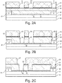
- FIG. 2 A method of fabricating a Group III nitride-based transistor device will now be described with reference to figure 2 , which includes figures 2A to 2J .
- the method may be used to fabricate the Group III nitride-based device illustrated in Figure 1 .
- the fabrication of a gate G and a field plate FP of a Group III nitride-based transistor device and subsequent layers of the conductive redistribution structure will be described.
- a substrate 40 comprising a Group III nitride-based layer 41 which includes a first passivation layer 42 arranged on a first major surface 43 of the Group III nitride-based layer 41 and a second passivation layer 44 arranged on the first passivation layer 42.
- the second passivation layer 44 is of a different composition from the first passivation layer 42.
- the first passivation layer 42 is formed from a nitride, for example a silicon nitride and the second passivation layer 44 is formed from an oxide, for example a silicon oxide, for example a TEOS layer.
- the first passivation layer 42 is typically thinner than the second passivation layer 44.
- the passivation layer 42 is formed of a high-k dielectric, for example a hafnium- or zirconium-based dielectric materials such as hafnium silicate, hafnium dioxide, zirconium silicate and zirconium dioxide. This enables the thickness d FP of the passivation layer between the lower surface of the field plate 63 and the first major surface 43 to be increased.
- the substrate 40 may include a foreign substrate formed of a material different to a Group III nitride.
- the foreign substrate may be formed of silicon or sapphire.
- the Group III nitride-based layer 41 may have a multi-layer structure including a buffer layer arranged on the foreign substrate 40, a channel layer arranged on the buffer layer and a barrier layer arranged on the channel layer to form a heterojunction.
- the Group III nitride-based layer 41 may have a structure according to one of the embodiments described with reference to figure 1 , for example.
- a source contact 45 and a drain contact 46 which are typically ohmic contacts, have already been formed on the Group III nitride-based layer 41.
- the source contact 45 and drain contact 46 extend partially or entirely through the thickness of the first passivation layer 42.
- the source contact 45 and the drain contact 46 are covered by the second passivation layer 44.
- a first mask layer 50 is formed on the second passivation layer 44.
- the first mask layer 50 includes a first insulating layer 51 arranged on the second passivation layer 44 and a first resist layer 52 arranged on the first insulating layer 51.
- the first insulating layer 51 may be referred to as a hard mask and may include titanium nitride and the first resist layer 52 may be a photolithographically definable polymer layer, for example a photoresist, and may be referred to as soft mask.
- a first opening 53 for a gate electrode (G) and a second opening 54 for a field plate (FP) are formed in the first mask layer 50.
- the first and second openings 53, 54 extend through the first photoresist layer 52 and the first insulating layer 51.
- one or more further openings 55 are formed above the source contact 45 and/or drain contact 46.
- FIG 2 the processing of an electrical connection to the ohmic drain contact 46 is illustrated since the connection structure to the source ohmic contact 45 is positioned in a plane of the transistor device which cannot be seen in the cross-sectional views of figure 2 .
- the electrical connections for the source ohmic contact, drain ohmic contact and gate and a field plate may also be formed at substantially the same time using appropriately positioned openings in the first mask layer 50.
- the source contact 45 and drain contact 46 may have an elongate strip-like structure with the length extending into the plane of the drawing.
- the gate and field plate may also have an elongate strip-like structure. Consequently, the openings 53, 54, 55 also have an elongate strip-like structure with the longest dimension, or length extending into the plane of the drawing.
- the second passivation layer 44 is exposed in the base of the first, second and further openings 53, 54, 55 of the first mask layer 50 and the exposed region is then removed, for example by etching.
- a first via 56 for the gate electrode is formed in the second passivation layer 44 which has a base formed by the first passivation layer 42.
- the second passivation layer 44 which is exposed by the second opening 54 is removed to form a second via 57 for a field plate.
- the second via 57 also has a base formed by the second passivation layer 42.
- a further via 58 may be formed in the second passivation layer 44 at a position above the drain ohmic contact 46 (and not seen in figure 2 , a further via for the source ohmic contact 45) which has a base formed by the respective ohmic contact 46, 45.
- the first photoresist layer 52 is then removed and a second photoresist layer 59 is applied.
- the first insulating layer 51 of the first mask layer 50 is not removed such that the second photoresist layer 59 is applied onto the first insulating layer 51.
- the second photoresist layer 59 covers the second via 57 for the field plate and also the vias 58 for the drain and source ohmic contacts but leaves the first via 56 for the gate uncovered. Therefore, the second resist layer 59 includes an opening 47 positioned above the first via 56.
- a region 48 of the first insulating layer 51 that is positioned immediately adjacent the first via 56 also remains uncovered by the second photoresist layer 59.
- the opening 47 formed in the second photoresist layer 59 is, therefore, laterally wider than the lateral width of the first via 56.
- the region of the first passivation layer 42 which is exposed at the base of the first via 56 is then removed using the exposed regions 48 of the first insulating layer 51 as a mask, as can be seen in figure 2C .
- the second resist layer 59 is then partially or completely removed.
- an electrically conductive material 60 is then inserted into the first via 56, the second via 57, the further via 58 and the unseen via positioned on top of the source ohmic contact.
- a planarisation process is then carried out to form a planarised surface 61 as illustrated in figure 2D .
- the conductive material 60 forms a conductive via 62 in the first via 56 which extends from the upper surface 61 of the planarised second passivation layer 44 through the entire thickness of the second passivation layer 44 and through at least part of the first passivation layer 42.
- the conductive material 60 of the first conductive via 62 is in contact with the Group III nitride material of the body 41.
- the conductive material 60 forms a second conductive via 63 in the second via 57 and a third conductive via 64 in the further opening 58.
- the conductive material 60 may include tungsten.
- the conductive material 60 may be copper. In other embodiments, the conductive material may comprise titanium nitride, tungsten nitride, tantalum nitride or aluminium.
- the conductive material 60 is formed on the first passivation layer 42 in the vias 57, 58 and on the surface 43 of the Group III nitride-based body 41 in the via 56.
- the first conductive via 62 forms the gate and the second conductive via 63 forms the field plate of the transistor device.
- the first conductive via 62 and the gate and the second conductive via 63 and field plate 63 may have an elongate strip like structure with the length extending into the plane of the drawing.
- the gate the field plate of the transistor device may therefore comprise tungsten or copper or titanium nitride, or tungsten nitride, or tantalum nitride or aluminium.
- the conductive material 60, the gate and the field plate may also include sublayers and have a multi-layer structure.
- the conductive material 60 may include one or more liner or barrier layers which are deposited on the side faces and optionally the base of the vias 56, 57, 58 formed in the second passivation layer 44.
- the liner may be formed on the first passivation layer 42 in the case of the vias 57, 58 and on the surface 43 of the Group III nitride-based body 41 in the via 56.
- a further conductive material for example tungsten, may be inserted into the lined vias to fill the via and form a conductive via.
- the liner or barrier layer may include Ti/TiN.
- the structure illustrated in figures 2A and 2D each have a planarized upper surface 61 which is particularly suitable for using as a base, onto which further layers of a three-dimensional redistribution structure of the transistor device can be built up.
- the accurate placement of the vias 56 and 57 for the gate and field plate enables a short gate length, L G , and small distance between the field plate and the gate, L GFP , to be achieved. Fabrication of the subsequent layers of the metallization structure can also be carried out with greater lateral precision in order that the distances can be maintained.
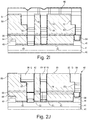
- a third passivation layer 65 is deposited on the planarized surface followed by a fourth passivation layer 66 on the third passivation layer 65.
- the third passivation layer 65 may be thinner than the fourth passivation layer 66.
- the third passivation layer 65 may include nitride such as a silicon nitride and the fourth passivation layer may include an oxide such as a silicon oxide, for example TEOS.
- the first and third passivation layers 42, 65 may include substantially the same composition and the second and fourth passivation layers 44, 66 may include substantially the same composition.
- a second mask 69 that includes two layers 67, 68 is formed on the fourth passivation layer 66.
- a second insulating layer 67 which may include titanium nitride, is formed on the fourth passivation layer 66 and a third resist layer 68 is formed on the second insulating layer 67 to form the second mask layer 69 having two layers of differing composition.
- the second mask layer 69 is structured to form a fourth opening 70 positioned above the conductive via 62 for the gate and a fifth opening 71 positioned above the conductive via 63 for the field plate and a sixth opening 72 positioned above the conductive via 64 for the drain 46.
- a further opening may also be positioned above the source which cannot be seen in the cross-sectional view of figure 2F .
- the openings 70, 71 and 72 extend through the third insulating layer 67 and the third photoresist layer 68 such that a portion of the fourth passivation layer 66 is exposed in the base of the fourth, fifth and sixth openings 70, 71, 72.
- a dual damascene process may be used to fabricate a conductive layer of the redistribution structure that vertically connects to the conductive vias 62, 63, 64 and that extends perpendicularly to the conductive vias 62, 63, 63 in lateral or horizontal directions.
- a two-stage process may be used to form an opening in the third and fourth passivation layers 65, 66 with a suitable form.
- the two layers 67, 68 of the second mask 69 may be used to form openings of two different lateral widths for removing portions of the fourth passivation layers 66 and for removing the third passivation layer 65.
- the conductive layer of the redistribution structure that vertically connects to the conductive vias 62, 63, 64 and that extends perpendicularly to the conductive vias 62, 63, 63 in lateral or horizontal directions may be formed of the same material as the first conductive layer 60 and comprise one or more of tungsten, copper, titanium nitride, tungsten nitride, tantalum nitride or aluminium.
- the third resist layer 68 is then removed and a fourth resist layer 73 applied which is positioned on the remaining portions of the third insulating layer 67 and on regions of the fourth passivation layer 66 positioned laterally adjacent the gate via 62 and drain via 64.
- the fourth resist layer 73 includes at least one opening 75 positioned above the gate via 62 and the field plate via 63 and at least one opening 76 positioned above the drain via 64.
- the openings 75, 76 are sized and positioned so as to form conductive vias through the thickness of the third and fourth passivation layers 65, 66 that are positioned at intervals along the elongate gate, field plate, drain and source respectively.
- the openings 75, 76 in the fourth resist layer 73 may be laterally smaller than the openings 70, 71, 72 in the remaining portion of the third insulating layer 67.
- the openings 70, 71, 72 in the remaining portion of the third insulating layer 67 may be elongate and correspond to the elongate gate, field plate and drain.
- the second passivation layer 66 that is exposed in the openings 75, 76 is also uncovered by the third insulating layer 67. These exposed regions are removed to form first indentations 77 positioned above the gate via 62, second indentations 78 positioned above the field plate via 63 and at least one third indentation 79 positioned above the drain via 64.
- the base of the indentations 77, 78, 79 is positioned within the fourth passivation layer 66.
- the fourth resist layer 73 is then removed and the remaining regions of the third insulating layer 67 are used as a mask, whereby remaining exposed portions of the fourth passivation layer 66 are removed.
- a first trench 80 is formed which has an upper portion that is laterally wider than a lower portion.
- the lower portion has a lateral size and position corresponding to the indentations 77 such that a plurality of vias 83 are formed that extend from the upper portion through the fourth passivation layer 66 and third passivation layer 65 such that a plurality of areas of the elongate gate via 62 is exposed at the bottom of the first trench 80.
- the vias 83 may have a substantially round, square or hexagonal form in plan view and be spaced at intervals along the length of the elongate gate via 62.
- the indentations 78 positioned above the field plate also extend through the entire thickness of the fourth passivation layer 66 and the third passivation layer 65 such that the base of a second trench 81 includes a plurality of vias 84 with a base formed by the conductive via 63 of the field plate.
- the vias 84 may have a substantially round, square or hexagonal form in plan view and be spaced at intervals along the length of the elongate field plate via 63.
- a third trench 82 is formed that is positioned above the drain via 64 also has an elongate upper portion and a plurality of a lower portions forming vias 85 positioned at intervals along the length of the drain via 64 that extend through the entire thickness of the third and fourth passivation layers 65, 66 and expose the upper surface of the via 64 to the drain contact 46.
- the trenches 80, 81, 82 and vias 83, 84, 85 extending from the base of the trenches 80, 81, 82 are then filled with conductive material 86.
- the conductive material 86 may include one or more layers and may include a barrier layer which lines the sidewalls of the respective trench and is positioned on the third passivation layer 65, fourth passivation layer 66 and on the remainder of the second insulating layer 67 positioned on the upper surface of the fourth passivation layer 66.
- the conductive layer 86 of the redistribution structure that vertically connects to the conductive vias 62, 63, 64 and that extends perpendicularly to the conductive vias 62, 63, 63 in lateral or horizontal directions may be formed of the same material as the first conductive layer 60 and comprise one or more of tungsten, copper, titanium nitride, tungsten nitride, tantalum nitride or aluminium.
- a planarisation process may then be carried out.
- the second insulating layer 67 may be used as a stop layer so that a planarised surface 89 is formed including material of the fourth passivation layer 66 and the conductive material positioned in the trenches 80, 81, 82.
- a conductive redistribution structure 90 is formed which has horizontal portions 86, 87, 88 formed by the upper portions of the trenches 80, 81, 82 and vertical conductive vias 83, 84, 85 formed by the lower portions.
- the horizontal conductive portions 86, 87, 88 and the vertical conductive vias 83, 84, 85 are formed using a single deposition process which may be referred to as a dual damascene process.
- the redistribution structure for the field plate includes different layers which include the conductive via 63 formed from the material of the first conductive layer 60 and the via 84 formed from the conductive layer 86.
- the conductive materials 60 and 86 may be different.
- the lower layer of the redistribution structure for example, the conductive material 60 comprises a material having a higher work function that the upper layer or layers, for example conductive material 86, comprises a material with a smaller electrical resistance. This arrangement may be used to optimise the properties of the redistribution structure in each layer separately.
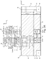
- Figures 3A to 3G each illustrate a top view in an X-Y plane and a cross-sectional view in an X-Z plane of a conductive redistribution structure. Lateral directions are depicted in the X-Y plane and vertical directions in the Z direction of the Cartesian coordinate system.
- Figure 3A illustrates a top view and a cross-sectional view along the line A-A of a metallization structure 90.
- the metallization structure 90 may be fabricated using the methods described with reference to figure 2 .
- the base of the gate 62 and the field plate 63 each have an elongate strip-like structure which extends in a longitudinal direction which is indicated in the drawings the Y direction.
- the gate 62 has a conductive redistribution structure formed by a plurality of upper portions 86 of the trench 80 that extend horizontally or transversely in the X direction and a plurality of gate vias 83 that are spaced at intervals along the gate 62 in the Y direction and electrically couple the gate 62 to the upper portion 86.
- One gate via 83 is positioned under and electrically connected to one upper portion 86.
- the metallization structure 90 includes a transverse metal strip 91 which extends from the conductive via 87 coupled to the field plate 67 over the lower portion of the gate 62 to the source in order to electrically couple the field plate 63 to source potential.
- the transverse portions 91 coupled to the field plate 63 and the transverse portions 86 coupled to the gate 62 extend parallel to one another in the X direction and are arranged alternately and spaced apart from one another in the Y direction.
- a portion of the fourth passivation layer 66 is positioned between the metal strip 91 and the gate 67 in the plane A-A. Along the line A-A, there is no conductive connection between the elongate field plate 63 and the conductive strip 91.
- the metallization structure 90 includes the lateral gate redistribution structure formed by the transverse portions 86 and a lateral field plate redistribution structure formed by the transvers portions 91 that are arranged in a plane above the plane of the gate electrode 62 and the field plate 63.
- the lateral gate redistribution structure and the lateral field plate redistribution structure are positioned at least partially above the active region of the Group III nitride-based transistor device since they are arranged laterally between the source electrode 45 and drain electrode 46.
- the gate electrode 62 is electrically coupled to the lateral gate redistribution structure 86 by one or more gate conductive vias 83 that are positioned laterally between the source electrode 45 and the drain electrode 46 in order to electrically connect the gate electrode 62 to the upper transverse portions 86.
- the one or more gate conductive vias 83 are arranged above the active region of the Group III nitride-based transistor device.
- the field plate 63 is electrically coupled to the lateral field plate redistribution structure 91 by one or more field plate conductive vias 84 that are positioned laterally between the source electrode 45 and the drain electrode 46 in order to electrically connect field plate 63 to the lateral field plate redistribution structure 91.
- the one or more field plate conductive vias 84 are arranged above the active region of the Group III nitride-based transistor device.
- Figure 3B illustrates a further top view of the metallization structure 90 and a cross-sectional view along the line B-B which lies outside of the lateral extent of the gate via 83.
- the horizontal or transverse portion 86 of the gate redistribution structure that is positioned above the gate 62 is vertically spaced apart from the gate 62 by a portion of the fourth passivation layer 66.
- Figure 3C illustrates a top view and a cross-sectional view along the line C-C of the redistribution structure 90 which illustrates the connection between the conductive strip 91, the conductive vias 84, 87 and the field plate 63.
- the elongate field plate 63 is electrically connected to the transverse strip 91 by one of the conductive vias 84, 87.
- the conductive strip 91 is spaced apart from the underlying gate 62 by a portion of the fourth passivation layer 66.
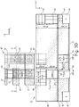
- Figure 3D illustrates a top view and a cross-sectional view of a redistribution structure 90' along the line D-D.
- the redistribution structure 90' differs from the redistribution structure 90 of figures 3A to 3C in the redistribution structure for the field plate 63.
- the upper portion 87 extends over the entire length of the field plate 63.
- the upper field plate 87 has an elongate structure and extends substantially parallel to the lower field plate 63 in the Y direction.
- the upper field plate portion 87 is connected by a plurality of conductive field plate vias 84 positioned at spaced intervals in the Y direction that extend between the field plate 63 and upper field plate portion 87.
- Figure 3D illustrates a cross-sectional view along the line D-D and the conductive connection between the gate 62 and the upper lateral gate portion 86 at a longitudinal position which includes the gate via 83.
- the field plate 63 does not include a conductive field plate via 84 between the lower field plate 63 and the upper field plate 87.
- the lower field plate 63 and the upper field plate 87 are spaced apart vertically, i.e. in the Z direction, by a portion of the fourth passivation layer 66.
- the transverse connections 86, 87 coupled to the gate 62 and field plate 63, respectively, are arranged alternately in the Y direction.
- the vias 62,83 for the gate and the vias 63, 84 for the field plate are also arranged alternately in the Y direction.
- Figure 3D illustrates a view of the redistribution structure 90' in which the upper field plate 87 has a longitudinal portion which is laterally wider in the X and Y directions than the field plate 63 positioned at the lower surface of the metallization structure 90 on the first passivation layer 61.
- This form of the upper field plate 87 provides a shielding structure.
- the redistribution structure for the field plate 63 includes a plurality of transverse portions 87 which extend above the gate 61 positioned in the first layer of the metallization structure 90.
- Transverse sections 86 of the gate redistribution structure are positioned between transverse portions of the field plate redistribution structure in the Y direction.
- the transverse portions 86 of the gate redistribution structure are electrically connected to the underlying gate trench 61 by the gate via 83 as can be seen in the cross-sectional view along the line D-D in figure 3D .
- Figure 3E illustrates a cross-sectional view of the redistribution structure 90' along the line E-E illustrates a cross-sectional view of the transverse field plate connection 87.
- the transverse field plate connection 87 extends over and above the gate 61 and is electrically insulated from the gate 61 by a vertically intervening portion of the third and fourth passivation layers 65, 66. In this position, the electrical connection between the transverse portion 87 and the field plate 62 by means of the field plate via 84 can be seen.
- Figure 3F illustrates a cross-sectional view of the redistribution structure 90' along the line F-F.
- the line F-F is positioned at a position in the longitudinal or Y direction of the gate 61 and field plate 63 in which no vias between the gate 62 and the field plate 63 and the upper surface 89 of the fourth passivation layer are positioned.
- the laterally wider transverse portions 87 provide a shielding structure for the field plate 63.
- the conductive vias 87 electrically connecting the field plate 62 to the overlying structure are spaced at intervals in the longitudinal direction of field plate 62.
- the conductive vias 87 electrically connecting the field plate 62 to the overlying structure are spaced at intervals in the longitudinal direction of field plate 62.
- the gate vias 83 are positioned in the longitudinal direction between the field plate vias 84. Therefore, alternate transverse portions 86, 87 are connected to the field plate and to gate can be seen in the top view of figure 3A .
- Figure 3G illustrates a top view and a cross-sectional view along the line G-G of a further embodiment in which the field plate 63 has a split field plate structure 100 such that two field plates 101, 102 are positioned between the gate 62 and the drain 46. The two field plates 101, 102 are spaced apart from one another by portions of the passivation layer 44.
- the first field plate structure 101 is positioned on the first passivation layer 42 and extends to the third passivation layer 65.
- the second passivation layer 44 is divided into two sublayers 103, 104 comprising an oxide material and a further fifth passivation layer 105, which comprises nitride, is positioned between the two sublayers 103, 104.
- the second field plate 102 is positioned on the fifth passivation layer 105 and extends vertically to the third passivation layer 65.
- the first field plate 101 that is portioned adjacent the gate 62 extends vertically through the lower sublayer 103, the fifth passivation layer 105 and the upper sublayer 104 to the third passivation layer 65.
- the lower sublayer 103 and the fifth passivation layer 105 may have a thickness such that the conductive surface 21 of the source and drain contact 45, 46 is positioned within the second sublayer 104 of the second passivation layer 44.
- the redistribution structure 90' for the field plate 63 includes a shielding effect provided by the upper conductive layer 87, since the upper conductive layer 87 has lateral dimensions which are greater than the lateral dimensions of the field plate 63 of the lower metallization layer that is positioned on the Group III nitride body 41.
- Figures 4 and 5 illustrate plan views in the X-Y plane of metallization structures according to various embodiments which can be used for a transistor device, such as the transistor device illustrated in figures 1 to 3 .
- the transistor device includes a single field plate 63 positioned between the gate 62 and drain 46 and in figure 5 the transistor device includes a split field plate 100 positioned between the gate 62 and drain 46.
- the ohmic drain contact and its conductive redistribution structure is not seen in figures 4 and 5 .
- Figure 4A illustrates a top view of a portion of a metallization structure 110 including a lower conductive layer 111 and an upper conductive layer 112 which is vertically spaced apart from the lower conductive layer 111 by one or more passivation layers that are not depicted in the drawing.
- the lower conductive layer 111 includes the ohmic source contact 45, the gate 62 and the field plate 63 which each have an elongate structure with a long direction extending in the longitudinal Y direction substantially parallel to one another.
- the upper conductive layer 112 provides a lateral redistribution structure for the gate 62 and a lateral redistribution structure for the field plate 63.
- the upper conductive layer 112 includes a U-shaped portion which has a longitudinal portion 113 extending in the Y direction over the entire length of the field plate 63 and transverse portions 114 which extend in the X direction and substantially perpendicularly to the longitudinal portion 113.
- the transverse portions 114 are spaced apart from one another in the Y direction.
- Each transverse portion 114 extends from above the field plate 63 over the gate 62 to above at least region of the source contact 45.
- Each transverse portion 114 is electrically coupled to the underlying source contact 45 by an elongate conductive via 115 which extends vertically through the passivation layers to the underlying source contact 45.
- the transverse portions 114 and longitudinal portion 113 are electrically coupled to the field plate 63 by one or more conductive vias 116 extending between the longitudinal portion 113 and the field plate 63.
- a single elongate via 116 is provided that extends vertically between the field plate 63 of the lower conductive layer 111 and the longitudinal portion 113 of the upper conductive layer 112 over substantially the entire length of the field plate 63 in the Y-direction, e.g. at least over at least 90% of the entire length of the field plate 63 in the Y-direction.
- the gate 62 is electrically connected to a transverse conductive portion 117 of the upper conductive layer 112 which extends in the X direction from a position above the gate 62 to a position above or laterally adjacent the source contact 45.
- the transverse portion 117 coupled to the gate 62 is laterally spaced apart from the transverse portions 114 and longitudinal portion 113 of the upper conductive layer 112.
- the transverse portion 117 is electrically coupled to the underlying gate 62 by a via 118. No further conductive structure need be provided for the source contact 45 since the source contact 45 is coupled to the field plate 63 by way of the vias 115, 116 and transverse portions 114 of the upper conductive layer 112. This arrangement may be considered to be a fully shielded structure.
- the extent of the transverse portions 114 in the Y-direction may be at least 50% of the length of the field plate 63 in the Y-direction, such as at least 80% thereof.
- This fully shielded structure allows for a particularly low Cgd.
- Figure 4B illustrates a metallization structure 110 that is similar to that in figure 4A . It differs in that each of the transverse portions 114 of the upper conductive layer 112 has a smaller extent in the longitudinal Y direction, i.e. less than 50% of the length of the field plate 63 in the Y-direction, such as less than or equal to 20% thereof.
- the gap between each of the transverse portions 114 and the transverse portion 117 coupled to the gate 62 is larger than in the embodiment illustrated in figure 4A .
- the length of the vias 115 extending between the source contact 45 and the respective transverse portion 114 is also smaller due to the reduced width of the transverse portion 114 in the Y direction.
- This arrangement may be considered to be a semi shielded structure and allows for a lower Cgs than the fully shielded structure and may still have a lower Cgd than the non-shielded structure described below.
- Figure 4C illustrates an embodiment in which the upper conductive layer 112 includes only transverse portions 114 extending between the vias 115, 116 which are electrically coupled to the source 45 and field plate 63 respectively.
- the two transverse portions 114 are spaced apart from one another and not coupled to one another in the upper conductive layer by a longitudinal portion.
- two vias 116 are used to couple the elongate field plate 63 to the transverse portions 114.
- This configuration may be referred to as a non-shielded structure which allows for a particularly low Cgs.
- Figure 5 illustrates plan views of metallization structures 120 for embodiments including a split field plate 100, in which two field plates 101, 102 that are positioned between the gate 62 and drain 46 and that extend substantially parallel to one another.
- the lower conductive layer 111 includes the source contact 45, gate 62 and the first and second field plates 101, 102, the second field plate 102 being positioned between the first field plate 101 and the drain 46.
- the longitudinal portion 113 of the upper conductive layer 112 extends in the longitudinal direction continuously over the two field plates 101, 102.
- the transverse portions 114 are electrically connected to the two field plates 101, 102 by conductive vias 116, 116'.
- the transverse portions 114 extend from above the two field plates 101, 102 over the gate 62 to above at least region of the source contact 45.
- Each transverse portion 114 is electrically coupled to the underlying source contact 45 by a conductive via 115 which extend through the passivation layers and to each of the field plates 101, 102 by a respective conductive via 116, 116'.
- the gate 62 is electrically connected to a transverse conductive portion 117 of the upper conductive layer 112 which extends in the X direction from above the gate 62 over the source contact 45 and which is laterally spaced apart from the transverse portions 114 and longitudinal portion 113 of the upper conductive layer 112.
- the transverse portion 117 is electrically coupled to the underlying gate 62 by a via 118. No further conductive structure need be provided for the source contact 45 since the source contact 45 is coupled to the field plates 101, 102 by way of the vias 115, 116, 116' and transverse portions 114 of the upper conductive layer 112. This arrangement may be considered to be a fully shielded structure.
- the upper conductive layer 112 includes illustrates a metallization structure 120 that is similar to that of figure 5A , but differs in that each of the transverse portions 114 of the upper conductive layer 112 has a smaller extent in the longitudinal Y direction.
- the gap between each transverse portion 114 that is coupled to the field plates 101, 102 and the transverse portion 117 that is coupled to the gate 62 is larger than in the embodiment illustrated in figure 4A .
- the length of the vias 115 extending between the source contact 45 and the respective transverse portion 114 is smaller due to the reduced width of the transverse portion 114 in the Y direction.
- Each transverse portion 114 extends over and is connected to the underlying two field plates 101, 102 by a single conductive via 116, 116' arranged on the field plates 101, 102, respectively.
- the upper conductive layer 112 includes only transverse portions 114 extending between the vias 115, 116, 116' which are electrically coupled to the source 45 and the two field plates 101, 102 respectively.
- the two transverse portions 114 are spaced apart from one another and not coupled to one another in the upper conductive layer 112 by a longitudinal portion.
- a first via 116 is used to couple the first elongate field plate 101 and a first via 116' is used to couple the second elongate field plate 102 to a first one of the transverse portions 114 and a second via 116 is used to couple the first elongate field plate 101 and a second via 116' is used to couple the second elongate field plate 102 to a second one of the transverse portions 114.
- Methods for fabricating an ohmic contact for Group III nitride-based transistor devices are disclosed that enable the fabrication of a device with a short gate length Lg, for example Lg ⁇ 250 nm, and an optimized feed-back capacitance Cgd.
- Such short gate lengths are useful for radio-frequency application transistors requiring a high transition frequency fT in the range 50 GHz to 150 GHz.
- this planarised surface after fabrication of the source and drain enables the subsequent layers built up upon it to be planar.
- This method enables the photoresist layer for the gate 62 and field plate 63 to be more accurately structured, since it is formed on a planar surface. As a result of the more accurate structuring of the photoresist layer, the dimensions and position of the gate 62 and field plate 63 can be more accurately controlled.
- the gate to source distance d SG may be less than 0,5 ⁇ m, for example 250nm or less in order to lower R DSON and enhance device performance.
- the more accurate structuring of the photoresist layer, the position of the field plate 63 with respect to the gate 62, d GPP can also be more reliably controlled and may also be less than 0,5 ⁇ m, for example 250nm or less .
- the gate length L G and/or the length of the field plate L FP may also be less than 0,5 ⁇ m, for example 250nm or less.
- This high precision patterning of the gate electrode is enabled as the photoresist processes of the gate and field plate are not affected by topography steps created by the Ohmic metal contacts 45, 46 due to the formation of the planarized surface. Such topography steps would impair the local uniformity of the involved anti-reflection-coating and resist coating processes and would degrade the depth-of-focus of the lithographic exposure process. In effect the control of small dimension lithographic structures would be severely limited.
Landscapes
- Junction Field-Effect Transistors (AREA)
- Electrodes Of Semiconductors (AREA)
- Engineering & Computer Science (AREA)
- Chemical & Material Sciences (AREA)
- Ceramic Engineering (AREA)
- Manufacturing & Machinery (AREA)
Abstract
Description
- To date, transistors used in power electronic applications have typically been fabricated with silicon (Si) semiconductor materials. Common transistor devices for power applications include Si CoolMOS®, Si Power MOSFETs, and Si Insulated Gate Bipolar Transistors (IGBTs). More recently, silicon carbide (SiC) power devices have been considered. Group III-N semiconductor devices, such as gallium nitride (GaN) devices, are now emerging as attractive candidates to carry large currents, support high voltages and to provide very low on-resistance and fast switching times. Further improvements to Group III nitride-based devices, are, however desirable.
- According to the invention, a method of fabricating a Group III nitride-based transistor comprises providing a substrate comprising a Group III nitride-based layer, a first passivation layer on the first major surface of the Group III nitride-based layer and a second passivation layer arranged on the first passivation layer, the second passivation layer having a different composition from the first passivation layer, forming a first mask layer on the second passivation layer, the first mask layer comprising a first insulating layer arranged on the second passivation layer and a first resist layer on the first insulating layer, forming a first opening for a gate electrode in the first mask layer, the first opening extending through the first resist layer and through the first insulating layer, forming a second opening for a field plate in the first mask layer, the second opening extending through the first resist layer and through the first insulating layer, removing the second passivation layer exposed by the first opening and forming a first via for the gate electrode, the first via having a base formed by the first passivation layer, removing the second passivation layer exposed by the second opening and forming a second via for a field plate, the second via having a base formed by the first passivation layer, removing the first resist layer, applying a second resist layer onto the first insulating layer that covers the second opening for the field plate and leaves the first opening for the gate electrode and a region of the first insulating layer adjacent he first opening uncovered, removing the first passivation layer exposed by first via and increasing the depth of the first via such that the first via has a base formed by the Group III nitride multi-layer structure, removing the second resist layer, and depositing an electrically conductive layer into the first via and the second via.
- In some embodiments, the first resist layer is a photoresist layer and the second resist layer is a photoresist layer. In some embodiments, the electrically conductive layer is a tungsten layer.
- In some embodiments, the method further comprises depositing the tungsten layer onto the second passivation layer laterally adjacent to the first via and the second via, and planarising to form a planarised surface comprising isolated areas of tungsten surrounded by the second passivation layer.
- In some embodiments, the second resist layer leaves a portion of the first insulating layer that is arranged adjacent the first via exposed.
- In some embodiments, the first insulating layer and the first photoresist are patterned using DUV (deep ultra violet) technology.
- In some embodiments, the base of the first via has a
width 30 nm to 500 nm, for example a width of around 250 nm or less or of 225nm to 350 nm, for example around 250nm and/or a minimum distance between the base of the first via and the second via is at theclosest point 30 nm to 500nm, or 225nm to 350 nm, for example 250nm or less. - In some embodiments, a base of the first via and a base of the second via each have a width of 50 nm to 400 nm, or 200nm to 350 nm, for example around 250nm and the distance between the first and second at the closest point is 100 nm to 400 nm, or 200nm to 350 nm, for example around 250nm.
- In some embodiments, the first passivation layer comprises silicon nitride, the second passivation layer comprises silicon oxide and the first insulating layer comprises titanium nitride.
- In some embodiments, the substrate further comprises a first ohmic contact and a second ohmic contact on the first major surface of the Group III nitride-based layer, the first passivation layer is located on the first major surface of the Group III nitride-based layer and extends between the first ohmic contact and the second ohmic contact and the second passivation layer is arranged on the first passivation layer and on the first ohmic contact and on the second ohmic contact.
- In some embodiments, the substrate comprises a first passivation layer arranged on the first major surface. In some embodiments the method further comprises forming the first ohmic contact and the second ohmic contact on the first major surface of the Group III nitride-based layer that extend at least partially through the first passivation layer, covering the first ohmic contact and the second ohmic contact with a first sublayer of passivation material, planarising to form an intermediate planarized surface comprising a surface of the first ohmic contact, a surface of the second ohmic contact and the first sublayer, and forming a second sublayer of passivation material on the planarized surface and arranged on the first ohmic contact and the second ohmic contact, the first and second sublayers forming the second passivation layer.
- In some embodiments, the method further comprises forming a structure for a second ohmic contact. The second ohmic contact may be a drain contact and the first ohmic contact may be a source contact. The structure for the first and second ohmic contacts may be formed using the same process, for example the same mask layers. The structure for the first and second ohmic contacts may be formed using the same process, for example the same mask layers, as for the gate and field plate(s).
- In some embodiments, the method further comprises forming a third opening in the first mask layer, the third opening extending through the first photoresist layer and the first insulating layer and being positioned above the second ohmic contact, removing the second passivation layer exposed in the third opening and forming a third via having a base exposing a portion of the second ohmic contact, covering the third via with the second resist layer, and after removal of the second resist layer further depositing the tungsten into the third via, and planarising to form a planarised surface comprising isolated areas of tungsten positioned in the first, second and third vias, each isolated area of tungsten being surrounded by the second passivation layer.
- In some embodiments, a second conductive layer of the metallization structure is fabricated.
- In some embodiments, the method further comprises forming a second insulation layer on the second passivation layer and on the isolated areas of tungsten, forming a third insulating layer on the second insulation layer, the second and third insulation layers having differing compositions, structuring the third insulation layer to form a first trench positioned above the first via, the first trench having a base spaced apart from the first via by a portion of the third insulating layer and the second insulating layer, the first trench being laterally wider than the first via, forming a fourth via in the base of the first trench that exposes the tungsten in the first via by removing the third insulation layer and the second insulation layer, the fourth via being laterally smaller than the first trench and forming a second tungsten layer in the fourth via and in the first trench.
- In some embodiments, trenches and vias for the gate and the field plate are formed in the second conductive level of metallization structure.
- In some embodiments, the method further comprises structuring the third insulation layer to form a second trench above the second via and a third trench above the third via, the second trench having a base spaced apart from the second via by a portion of the third insulating layer and the second insulating layer, the second trench being laterally wider than the second via, the third trench having a base spaced apart from the third via by a portion of the third insulating layer and the second insulating layer, the third trench being laterally wider than the third via, forming a fifth via in the second trench that exposes the tungsten in the second via by removing the third insulation layer in the base of the second trench, forming a sixth via in the third trench that exposes the tungsten in the third via by removing the third insulation layer in the base of the third trench, and depositing the second tungsten layer into the second and third trenches and into the fifth and sixth vias.
- In an embodiment, a Group III nitride-based transistor device comprises a source electrode, a drain electrode and a gate electrode positioned on a first major surface of a Group III nitride based-based layer, wherein the gate is laterally arranged between the source electrode and the drain electrode, and a field plate, the field plate being laterally arranged between and spaced apart from the gate electrode and the drain electrode. A base of the gate electrode and a base of the field plate each have a width of 50 nm to 400 nm, or 200nm to 350 nm, for example around 250nm and the distance between the gate electrode and the field plate at the closest point is 100 nm to 400 nm, or 200nm to 350 nm, for example around 250nm. According to the invention, a Group III nitride-based transistor device is provided that comprises a first passivation layer arranged on a first major surface of a Group III nitride based-based layer, a second passivation layer arranged on the first passivation layer, a source ohmic contact, a drain ohmic contact and a gate positioned on the first major surface of a Group III nitride based-based layer, wherein the gate is laterally arranged between the source ohmic contact and the drain ohmic contact and comprises a gate via extending to an upper surface of the second passivation layer, a field plate, the field plate being laterally arranged between and spaced apart from the gate and the drain ohmic contact and extending to an upper surface of the second passivation layer, a first via extending from the source ohmic contact to an upper surface of the second passivation layer, a second via extending from the drain ohmic contact to the upper surface of the second passivation layer, wherein the second passivation layer covers peripheral regions of the source ohmic contact and the drain ohmic contact, and a first substantially planar insulating layer arranged on the upper surface of the second passivation layer and on peripheral regions of the gate electrode, the field plate, the first via and the second via.
- In some embodiments, the source ohmic contact comprises a base portion having a conductive surface, the conductive surface comprising a peripheral portion and a central portion, the peripheral portion and the central portion being substantially coplanar and being of differing composition.
- In some embodiments, the first via is positioned on the central portion of the conductive surface.
- In some embodiments, the drain ohmic contact comprises a base portion having a conductive surface, the conductive surface comprising a peripheral portion and a central portion, the peripheral portion and the central portion being substantially coplanar and being of differing composition.
- In some embodiments, the second via is positioned on the central portion of the conductive surface.
- In some embodiments, the central portion comprises TiN and the peripheral portion comprises aluminium or an aluminium copper or a titanium aluminium alloy.
- In some embodiments, a base of the field plate is in direct contact with the first passivation layer, a base of the gate via is in direct contact with the first major surface, the source ohmic contact extends at least partially through the first passivation layer, and the drain ohmic contact extends at least partially through the first passivation layer.
- In some embodiments, the field plate extends substantially perpendicular to the first major surface and is electrically coupled to the source electrode by a lateral field plate redistribution structure that extends over and is spaced apart from the gate electrode.
- In some embodiments, the source electrode, the gate electrode, the drain electrode and the field plate each have an elongate form and extend on the first major surface in a longitudinal direction substantially parallel to one another.
- In some embodiments, the lateral field plate redistribution structure comprises a longitudinal section positioned above the field plate and extending substantially parallel to the longitudinal direction and a plurality of transverse sections spaced at intervals in the longitudinal direction, each transverse section extending over and being spaced apart from the gate electrode and being electrically coupled to the field plate by a field plate conductive via.
- In some embodiments, the Group III nitride-based transistor device further comprises a lateral gate redistribution structure, the lateral gate distribution structure comprising a plurality of transverse sections that extend substantially perpendicularly to the longitudinal direction, each transverse section being spaced apart from the gate electrode and electrically coupled to the gate electrode by a gate conductive via, the transverse section of the lateral gate distribution structure being interleaved with the transverse sections of the lateral field plate distribution structure.
- In some embodiments, the source electrode is electrically coupled to the lateral field plate redistribution structure.
- In some embodiments, the Group III nitride-based transistor device further comprises a source redistribution structure,, wherein the source electrode is electrically coupled by one or more source conductive vias to the source redistribution structure and the source redistribution structure is integral with the transverse sections of the field plate redistribution structure.
- In some embodiments, the source redistribution structure is formed of the source conductive vias and includes no lateral redistribution structure in the plane of the field plate redistribution structure.
- In some embodiments, the source redistribution structure includes a longitudinal section extending in the longitudinal direction and arranged above and spaced apart from the source electrode. The longitudinal section of the source redistribution structure may be substantially coplanar with the longitudinal and transverse sections of the lateral field plate redistribution structure. The longitudinal section of the source redistribution structure may also be substantially coplanar with the later gate redistribution structure.
- In some embodiments, the longitudinal section of the lateral field plate redistribution structure is laterally wider than the field plate.
- In some embodiments, the field plate is spilt into two field plate sections that extend substantially parallel to one another and are laterally spaced apart from one another, the two field plate sections being laterally arranged between and spaced apart from the gate electrode and the drain electrode.
- According to the invention, a Group III nitride-based transistor device is provided that comprises a source electrode, a drain electrode and a gate electrode positioned on a first major surface of a Group III nitride based-based layer, wherein the gate is laterally arranged between the source electrode and the drain electrode, a passivation layer arranged on the first major surface and a field plate coupled to the source electrode. The field plate has a lower surface arranged on the passivation layer and is laterally arranged between and laterally spaced apart from the gate electrode and the drain electrode. The source electrode, the gate electrode, the drain electrode and the field plate each have an elongate form and extend on the first major surface in a longitudinal direction substantially parallel to one another. The Group III nitride-based transistor device further comprises a conductive redistribution structure that is arranged above the source electrode, the gate electrode, the drain electrode and the field plate and comprises a lateral gate redistribution structure and a lateral field plate redistribution structure that are substantially coplanar at a position laterally between the source electrode and the drain electrode.
- In this Group III nitride-based transistor device, the lateral gate redistribution structure and the lateral field plate redistribution structure are arranged in a plane above the plane of the gate electrode and the field plate. The lateral gate redistribution structure and the lateral field plate redistribution structure are positioned at least partially above the active region of the Group III nitride-based transistor device since they are arranged laterally between the source electrode and drain electrode.
- In some embodiments, an upper surface of the field plate and an upper surface of the gate electrode are substantially coplanar.
- In some embodiments, the gate electrode is electrically coupled to the lateral gate redistribution structure by one or more gate conductive vias.
- In some embodiments, the one or more gate conductive vias are positioned laterally between the source electrode and the gate electrode in order to electrically connect the gate electrode to the lateral gate redistribution structure. The one or more gate conductive vias are arranged above the active region of the Group III nitride-based transistor device.
- In some embodiments, the field plate is electrically coupled to the lateral field plate redistribution structure by one or more field plate conductive vias.
- In some embodiments, the one or more field plate conductive vias are positioned laterally between the source electrode and the drain electrode in order to electrically connect field plate to the lateral field plate redistribution structure. The one or more field plate conductive vias are arranged above the active region of the Group III nitride-based transistor device.
- In some embodiments, an upper surface of the source electrode and an upper surface of the drain electrode are substantially coplanar and arranged at a distance above the first major surface that is less than the distance between the upper surface of the gate electrode and the first major surface. This arrangement allows the source and drain electrode to be fabricated before the gate electrode and field plate.
- In some embodiments, the source electrode is electrically coupled to the lateral field plate redistribution structure by one or more source conductive vias. The field plate is coupled to source potential in these embodiments.
- In some embodiments, the lateral field plate redistribution structure extends over and is spaced apart from the gate electrode. This enables the lateral field plate redistribution structure to act as a shield for the gate electrode that is positioned underneath and spaced at a distance from the lateral field plate redistribution structure.
- In some embodiments, the lateral field plate redistribution structure comprises a plurality of transverse sections spaced at intervals in the longitudinal direction, each transverse section extending over and being spaced apart from the gate electrode and being electrically coupled to the field plate by a field plate conductive via.
- In some embodiments, the transverse sections together cover less than 50% or less than 20% of a length of the gate electrode. This arrangement may be described as a partially shielded structure.
- In some embodiments, the transverse sections together cover at least 50% or at least 80% of a length of the gate electrode. This arrangement may be described as a shielded or fully shielded structure.
- In some embodiments, the transverse sections of the lateral field plate structure are arranged above and spaced apart from the source electrode and the source electrode is electrically coupled by one or more source conductive vias to the transverse sections of the field plate redistribution structure. In this arrangement, the source conductive vias and the field plate conductive vias are arranged adjacent and spaced apart from opposing sides of the gate electrode.
- In some embodiments, the lateral field plate redistribution structure further comprises a longitudinal section positioned above the field plate and extending substantially parallel to the longitudinal direction and to the field plate, wherein the longitudinal section is connected to the transverse sections. This arrangement may be used to increase the fielding of the gate electrode.
- In some embodiments, the longitudinal section of the lateral field plate redistribution structure is laterally wider than the conductive vias and the field plate. This arrangement may be used to further increase the fielding of the gate electrode.
- In some embodiments, the field plate is spilt into two field plate sections that extend substantially parallel to one another and are laterally spaced apart from one another, the two field plate sections being laterally arranged between and spaced apart from the gate electrode and the drain electrode.
- In some embodiments, the lateral gate distribution structure comprises a plurality of transverse sections spaced at intervals in the longitudinal direction, each transverse section being spaced apart from the gate electrode and electrically coupled to the gate electrode by a gate conductive via.
- In some embodiments, the transverse sections of the lateral gate redistribution structure are interleaved with the transverse sections of the lateral field plate distribution structure.
- In some embodiments, an upper surface of the lateral gate redistribution structure is substantially coplanar with an upper surface of the lateral field plate distribution structure.
- In some embodiments, the transverse sections of the lateral gate redistribution structure extend over and are spaced apart from the source electrode.
- In some embodiments, the lateral gate redistribution structure further comprises a longitudinal section that is positioned on an opposing side of the source electrode from the gate electrode and the transverse sections of the lateral gate redistribution structure are connected to the longitudinal section. In this arrangement, the lateral gate redistribution structure may also provide the gate pad with the lateral redistribution from the gate pad to the gate electrode being and substantially coplanar with the lateral field plate and drain redistribution structures. The vertical connection between the gat electrode and the lateral gate redistribution structure of the upper level is arranged directly above the gate electrode, i.e. by the one or more gate conductive vias extending between the gate electrode and the lateral gate redistribution structure, in the active area of the Group III nitride transistor device at a position laterally between the source and drain electrodes.
- Those skilled in the art will recognize additional features and advantages upon reading the following detailed description, and upon viewing the accompanying drawings.
- The elements of the drawings are not necessarily to scale relative to each other. Like reference numerals designate corresponding similar parts. The features of the various illustrated embodiments can be combined unless they exclude each other. Exemplary embodiments are depicted in the drawings and are detailed in the description which follows.
-
Figure 1 illustrates a Group III nitride-based transistor device according to an embodiment. -
Figure 2 , which includesfigures 2A to 2J , illustrates a method of fabricating a Group III nitride-based transistor device according to an embodiment. -
Figure 3 , which includesfigures 3A to 3G , illustrates plan views and cross-sectional views of Group III nitride-based transistor devices according to embodiments. -
Figure 4 , which includesfigures 4A to 4C , illustrates plan views of a metallization structure for a Group III nitride-based transistor device according to embodiments. -
Figure 5 , which includesfigures 5A to 5C , illustrates plan views of a metallization structure for a Group III nitride-based transistor device according to embodiments. - In the following detailed description, reference is made to the accompanying drawings, which form a part hereof, and in which is shown by way of illustration specific embodiments in which the invention may be practiced. In this regard, directional terminology, such as "top", "bottom", "front", "back", "leading", "trailing", etc., is used with reference to the orientation of the figure(s) being described. Because components of the embodiments can be positioned in a number of different orientations, the directional terminology is used for purposes of illustration and is in no way limiting. It is to be understood that other embodiments may be utilized and structural or logical changes may be made without departing from the scope of the present invention. The following detailed description, thereof, is not to be taken in a limiting sense, and the scope of the present invention is defined by the appended claims.
- A number of exemplary embodiments will be explained below. In this case, identical structural features are identified by identical or similar reference symbols in the figures. In the context of the present description, "lateral" or "lateral direction" should be understood to mean a direction or extent that runs generally parallel to the lateral extent of a semiconductor material or semiconductor carrier. The lateral direction thus extends generally parallel to these surfaces or sides. In contrast thereto, the term "vertical" or "vertical direction" is understood to mean a direction that runs generally perpendicular to these surfaces or sides and thus to the lateral direction. The vertical direction therefore runs in the thickness direction of the semiconductor material or semiconductor carrier.
- As employed in this specification, when an element such as a layer, region or substrate is referred to as being "on" or extending "onto" another element, it can be directly on or extend directly onto the other element or intervening elements may also be present. In contrast, when an element is referred to as being "directly on" or extending "directly onto" another element, there are no intervening elements present.
- As employed in this specification, when an element is referred to as being "connected" or "coupled" to another element, it can be directly connected or coupled to the other element or intervening elements may be present. In contrast, when an element is referred to as being "directly connected" or "directly coupled" to another element, there are no intervening elements present.
- As used herein, the phrase "Group III-Nitride" refers to a compound semiconductor that includes nitrogen (N) and at least one Group III element, including aluminum (Al), gallium (Ga), indium (In), and boron (B), and including but not limited to any of its alloys, such as aluminum gallium nitride (AlxGa(1-x)N), indium gallium nitride (InyGa(1-y)N), aluminum indium gallium nitride (AlxInyGa(1-x-y)N), gallium arsenide phosphide nitride (GaAsaPbN(1-a-b)), and aluminum indium gallium arsenide phosphide nitride (AlxInyGa(1-x-y)AsaPbN(1-a-b)), for example. Aluminum gallium nitride and AlGaN refers to an alloy described by the formula AlxGa(1-x)N, where 0 < x < 1.
- Methods for fabricating an ohmic contact for Group III nitride-based devices, such as transistor devices, are used that enable the fabrication of a device with a short gate length Lg, for example Lg ≤ 250 nm, and an optimized feed-back capacitance Cgd. Such short gate lengths are useful for radio-frequency application transistors requiring a high transition frequency fT in the
range 50 GHz to 150 GHz. Such short gate lengths can be achieved using high precision patterning for which photolithography processes with thin photo resist flows are required. - However, the processing of such photoresists is highly sensitive to topography steps on a wafer, such as steps created by the Ohmic Metal of the source and drain contacts that is fabricated prior to the gate structure.
- This disclosure makes use of an ohmic metallization concept which leaves no topography steps such as vertical steps due to RIE (Reactive Ion Etching) patterning of the Ohmic metal stack for the source and drain contacts so that photolithography can be applied to form shorter gate lengths and to position the gate more closely to the source contact to reduce RDSON. The methods can be carried out using the process capabilities of a 200 mm CMOS production line and, therefore, cost effectively on wafers having a diameter of at least 200 mm.
- According to the present disclosure, an Ohmic contact-first approach is used to fabricate a Group III nitride-based device, in particular a transistor device such as a HEMT (High Electron Mobility Transistor). In an embodiment, the method is carried out on a wafer, which may have a diameter of 6 inches or more, and includes planarizing the Ohmic metal before the fabrication of the gate structure. The ohmic metal may be formed by opening a window in the Group III nitride passivation, depositing an Ohmic metal stack, structuring the Ohmic metal stack and applying the Ohmic metal anneal step to alloy the ohmic metal. The ohmic metal can be planarized by depositing a CMP (Chemical Mechanical Polishing) stop layer on the frontside of the wafer, using chemical mechanical polishing on the structured Ohmic metal to produce a planarized surface and afterwards stripping the remaining parts of the stop layer.
- The planarized surface is used for the further processing of the device, for example to form the gate using photolithography without underlying topography affecting the accuracy of the photolithographic process. Advantages of this approach include enabling of a low gate to source distance to enhance device performance and improving the critical dimension control of the gate process to enhance manufacturability and device performance.
-
Figure 1 illustrates a schematic cross-sectional view of a Group III nitride-baseddevice 10 according to an embodiment. The Group III nitride-baseddevice 10 includes a Group III nitride-basedlayer 11, a firstohmic contact 12, a secondohmic contact 13 and agate 14, which are arranged on a firstmajor surface 15 of the Group III nitride-basedlayer 11. The Group III nitride-baseddevice 10 may be atransistor device 16 such as a High Electron Mobility Transistor (HEMT). In embodiments in which the GroupIII nitride device 10 is atransistor device 16, the firstohmic contact 12 may provide a source contact and the secondohmic contact 13 may provide a drain contact. Thegate 14 is arranged laterally between thesource contact 12 and thedrain contact 13. The Group III nitride-baseddevice 10 also includes afield plate 17 that is positioned on the firstmajor surface 15 and laterally between and spaced apart from thegate 14 and thedrain contact 13. - The Group III nitride-based
device 10 includes afirst passivation layer 18 arranged on the firstmajor surface 15 of the Group III nitride-basedlayer 11 and asecond passivation layer 19 arranged on thefirst passivation layer 18. - The
source contact 12, thegate 14 and thedrain contact 15 extend through thefirst passivation layer 18, whereas thefield plate 17 is arranged on thefirst passivation layer 18 and spaced apart from the underlying Group III nitride-basedlayer 11 by thefirst passivation layer 18. In some embodiments, thesource contact 12, thegate 14 and thedrain contact 15 are in direct contact with the Group III nitride-basedlayer 11. - Each of the first and second
ohmic contacts base portion 20 having an upperconductive surface 21 that is positioned within thesecond passivation layer 19. Each of theohmic contacts ohmic contacts gate 14 and thefield plate 17. Thegate 14 and thefield plate 17 are each formed of conductive material and extend through the entire thickness of thesecond passivation layer 19. Thegate 14 includes a gate via and thefield plate 17 includes a field plate via. Thegate 14 may be a Schottky contact. In other embodiments, thetransistor device 16 includes an insulated gate contact. - The first and second
ohmic contacts conductive surface 21 and that extends through thesecond passivation layer 19 to the upper surface. Theconductive surface 21 has aperipheral portion 24 andcentral portion 25 that are substantially coplanar and are of differing composition. The conductive via 22, 23 is positioned on thecentral portion 25 and has a lateral extent which is less than the lateral extent of thebase portion 20. In some embodiments, the lateral extent of the conductive via 22, 23 is less than the lateral extent of thecentral portion 25 of theconductive surface 21. - The Group III nitride-based
layer 11 may include a multilayer Group III nitride structure positioned on asupport substrate 27 which has agrowth surface 28 which is capable of supporting the epitaxial growth of at least one Group III nitride layer. Thesupport substrate 27 may be monocrystalline silicon substrate, for example a <111> or <110> silicon wafer or a monocrystalline sapphire substrate. - The multilayer Group
III nitride structure 11 may include a Group IIInitride buffer structure 29 arranged on thegrowth surface 28, a Group IIInitride channel layer 30 arranged on the Group IIInitride buffer structure 29 and a Group IIInitride barrier layer 31 arranged on the Group IIInitride channel layer 30. The Group IIInitride barrier layer 31 has a different composition and bandgap to the Group IIInitride channel layer 30 such that aheterojunction 32 is formed therebetween. For example, the Group IIInitride channel layer 30 may comprise gallium nitride and the Group IIInitride barrier layer 31 may comprise aluminium gallium nitride. Theheterojunction 32 is capable supporting a two-dimensional charge gas which is indicated schematically in the infigure 1 by the dashedline 33. The firstohmic contact 12 and the secondohmic contact 13 form an ohmic contact with the two-dimensional charge gas 33. - A
typical buffer structure 29 for a silicon substrate includes a AlN starting layer, which may have a thickness of several 100nm, on the silicon substrate followed by a AlxGa(1-x)N layer sequence, the thickness again being several 100nm's for each layer, whereby the Al content of about 50-75% is decreased down to 10-25% before the GaN layer of AlGaN back barrier is grown. Alternatively, a superlattice buffer can be used. Again, an AlN starting layer on the silicon substrate is used. Depending on the chosen superlattice, a sequence of AlN and AlxGa(1-x)N pairs is grown, where the thickness of the AlN layer and AlxGa(1-x)N is in the range of 2-25nm. Depending on the desired breakdown voltage the superlattice may include between 20 and 100 pairs. Alternatively, an AlxGa(1-x)N layer sequence as described above can be used in combination with the above mentioned superlattice. - As is indicated by the dotted line 35 in
figure 1 , thesecond passivation layer 19 includes two sublayers. Thelower sublayer 36 is positioned on the Group III nitride-basedbarrier layer 30 and, during manufacture of the Group III nitride-baseddevice 10, forms a planar surface with theconductive surface 21 of thebase portion 20 of the first and secondohmic contacts upper sublayer 37 onto the planar surface. The lower andupper sublayers - The
first passivation layer 18 is positioned between the upper surface of the Group III nitride-basedbarrier layer 30 and has a different composition to thesecond passivation layer 19. For example, thefirst passivation layer 18 may be formed of silicon nitride. - In some embodiments, the
passivation layer 18 is formed of a so called "high-k" dielectric, which has a higher dielectric constant compared to silicon dioxide, for example a hafnium- or zirconium-based dielectric materials such as hafnium silicate, hafnium dioxide, zirconium silicate and zirconium dioxide. This enables the thickness dFP of thepassivation layer 18 between the lower surface of thefield plate 17 and the firstmajor surface 15 to be increased, leakage to be avoided and reliability to be improved for these thin passivation layers. - The formation of this planarised surface 35, represented by the dotted line 35, enables the subsequent layers built up upon it to be planar. This enables the
gate 14 andfield plate 17 to be formed using photolithographic techniques after the fabrication of theohmic contacts gate 14 andfield plate 17 can be carried out on this planarised surface 35. - This method enables the photoresist layer for the
gate 14 andfield plate 17 to be more accurately structured, since it is formed on a planar surface 35 and can be formed after theohmic contacts Group III structure 11, which typically involves higher processing temperatures. As a result of the more accurate structuring of the photoresist layer, the dimensions and position of thegate 14 andfield plate 17 can be more accurately controlled. This also enables the distance dSG between theohmic source contact 12 and thegate 14, as measured at the base of theohmic contact 12 andgate 14, to be reduced and to be reliably produced at this reduced length. The gate to source distance dSG may be less than 0,5 µm, for example 250nm or less in order to lower RDSON and enhance device performance. The more accurate structuring of the photoresist layer, the position of thefield plate 17 with respect to the gate, dGPP, can also be more reliably controlled and may also be less than 0,5 µm, for example 250nm or less. - Additionally, the critical dimension control of the gate process is improved to enhance manufacturability and device performance. The gate length LG and/or the length of the field plate LFP may also be less than 0,5 µm, for example 250nm or less. This high precision patterning of the gate electrode is enabled as the photoresist processes of the gate and field plate are not affected by topography steps created by the
Ohmic metal contacts base portion 16. Such topography steps would impair the local uniformity of the involved anti-reflection-coating and resist coating processes and would degrade the depth-of-focus of the lithographic exposure process. In effect the control of small dimension lithographic structures would be severely limited. - In some embodiments, a base of the gate electrode and a base of the field plate each have a width of 50 nm to 400 nm, or 200nm to 350 nm, for example around 250nm and the distance between the gate electrode and the field plate at the closest point is 100 nm to 400 nm, or 200nm to 350 nm, for example around 250nm.
- In some embodiments, the upper
conductive surface 21 of theohmic contacts ohmic contacts - As discussed above, in some embodiments, the upper
conductive surface 21 of theohmic contacts regions central portion 25 andperipheral portion 24 may be provided as the upper surface of abase portion 20 that includes a well 38 comprising a metal or alloy of a first composition extending into alower portion 39 comprising a metal or alloy of a second different composition. The upper surface of the well 38 provides thecentral portion 25 of theconductive surface 21 and the upper surface of thelower portion 39 provides theperipheral portion 24 of theconductive surface 21, so that the upper surface of the well 38 and the upper surface of thelower portion 39 are substantially coplanar. - In some embodiments, the well 38 and the
central portion 25 of theconductive surface 21 comprise a conductive barrier material and thelower portion 39 andperipheral portion 24 comprise an ohmic contact material. An ohmic contact material is material which forms an ohmic contact to the Group III nitride material of the uppermost Group III nitride layer of the multilayer GroupIII nitride structure 11. In some embodiments, the conductive barrier material of the well 38 and thecentral portion 25 of theconductive surface 21 comprise titanium nitride and thelower portion 39 andperipheral portion 24 of theconductive surface 21 comprise aluminium or aluminium copper alloy or a titanium aluminium alloy. - The
base portion 20 of theohmic contacts - A method of fabricating a Group III nitride-based transistor device will now be described with reference to
figure 2 , which includesfigures 2A to 2J . The method may be used to fabricate the Group III nitride-based device illustrated inFigure 1 . In particular, the fabrication of a gate G and a field plate FP of a Group III nitride-based transistor device and subsequent layers of the conductive redistribution structure will be described. - A
substrate 40 comprising a Group III nitride-basedlayer 41 is provided which includes afirst passivation layer 42 arranged on a firstmajor surface 43 of the Group III nitride-basedlayer 41 and asecond passivation layer 44 arranged on thefirst passivation layer 42. Thesecond passivation layer 44 is of a different composition from thefirst passivation layer 42. In some embodiments, thefirst passivation layer 42 is formed from a nitride, for example a silicon nitride and thesecond passivation layer 44 is formed from an oxide, for example a silicon oxide, for example a TEOS layer. Thefirst passivation layer 42 is typically thinner than thesecond passivation layer 44. - In some embodiments, the
passivation layer 42 is formed of a high-k dielectric, for example a hafnium- or zirconium-based dielectric materials such as hafnium silicate, hafnium dioxide, zirconium silicate and zirconium dioxide. This enables the thickness dFP of the passivation layer between the lower surface of thefield plate 63 and the firstmajor surface 43 to be increased. - The
substrate 40 may include a foreign substrate formed of a material different to a Group III nitride. For example, the foreign substrate may be formed of silicon or sapphire. The Group III nitride-basedlayer 41 may have a multi-layer structure including a buffer layer arranged on theforeign substrate 40, a channel layer arranged on the buffer layer and a barrier layer arranged on the channel layer to form a heterojunction. The Group III nitride-basedlayer 41 may have a structure according to one of the embodiments described with reference tofigure 1 , for example. - A
source contact 45 and adrain contact 46, which are typically ohmic contacts, have already been formed on the Group III nitride-basedlayer 41. Thesource contact 45 anddrain contact 46 extend partially or entirely through the thickness of thefirst passivation layer 42. Thesource contact 45 and thedrain contact 46 are covered by thesecond passivation layer 44. - A
first mask layer 50 is formed on thesecond passivation layer 44. Thefirst mask layer 50 includes a first insulatinglayer 51 arranged on thesecond passivation layer 44 and a first resistlayer 52 arranged on the first insulatinglayer 51. In some embodiments, the first insulatinglayer 51 may be referred to as a hard mask and may include titanium nitride and the first resistlayer 52 may be a photolithographically definable polymer layer, for example a photoresist, and may be referred to as soft mask. Afirst opening 53 for a gate electrode (G) and asecond opening 54 for a field plate (FP) are formed in thefirst mask layer 50. The first andsecond openings first photoresist layer 52 and the first insulatinglayer 51. - In some embodiments one or more
further openings 55 are formed above thesource contact 45 and/or draincontact 46. Infigure 2 , the processing of an electrical connection to theohmic drain contact 46 is illustrated since the connection structure to the sourceohmic contact 45 is positioned in a plane of the transistor device which cannot be seen in the cross-sectional views offigure 2 . The electrical connections for the source ohmic contact, drain ohmic contact and gate and a field plate may also be formed at substantially the same time using appropriately positioned openings in thefirst mask layer 50. - The
source contact 45 anddrain contact 46 may have an elongate strip-like structure with the length extending into the plane of the drawing. The gate and field plate may also have an elongate strip-like structure. Consequently, theopenings - The
second passivation layer 44 is exposed in the base of the first, second andfurther openings first mask layer 50 and the exposed region is then removed, for example by etching. - Referring to
Figure 2B , a first via 56 for the gate electrode is formed in thesecond passivation layer 44 which has a base formed by thefirst passivation layer 42. Similarly, thesecond passivation layer 44 which is exposed by thesecond opening 54 is removed to form a second via 57 for a field plate. The second via 57 also has a base formed by thesecond passivation layer 42. A further via 58 may be formed in thesecond passivation layer 44 at a position above the drain ohmic contact 46 (and not seen infigure 2 , a further via for the source ohmic contact 45) which has a base formed by the respectiveohmic contact - Referring to
figure 2C , thefirst photoresist layer 52 is then removed and asecond photoresist layer 59 is applied. The first insulatinglayer 51 of thefirst mask layer 50 is not removed such that thesecond photoresist layer 59 is applied onto the first insulatinglayer 51. Thesecond photoresist layer 59 covers the second via 57 for the field plate and also thevias 58 for the drain and source ohmic contacts but leaves the first via 56 for the gate uncovered. Therefore, the second resistlayer 59 includes anopening 47 positioned above the first via 56. Aregion 48 of the first insulatinglayer 51 that is positioned immediately adjacent the first via 56 also remains uncovered by thesecond photoresist layer 59. Theopening 47 formed in thesecond photoresist layer 59 is, therefore, laterally wider than the lateral width of the first via 56. - The region of the
first passivation layer 42 which is exposed at the base of the first via 56 is then removed using the exposedregions 48 of the first insulatinglayer 51 as a mask, as can be seen infigure 2C . The second resistlayer 59 is then partially or completely removed. - Referring to
figure 2D , an electricallyconductive material 60 is then inserted into the first via 56, the second via 57, the further via 58 and the unseen via positioned on top of the source ohmic contact. - In some embodiments, a planarisation process is then carried out to form a
planarised surface 61 as illustrated infigure 2D . Theconductive material 60 forms a conductive via 62 in the first via 56 which extends from theupper surface 61 of the planarisedsecond passivation layer 44 through the entire thickness of thesecond passivation layer 44 and through at least part of thefirst passivation layer 42. In some embodiments, theconductive material 60 of the first conductive via 62 is in contact with the Group III nitride material of thebody 41. Theconductive material 60 forms a second conductive via 63 in the second via 57 and a third conductive via 64 in thefurther opening 58. Theconductive material 60 may include tungsten. In other embodiments, theconductive material 60 may be copper. In other embodiments, the conductive material may comprise titanium nitride, tungsten nitride, tantalum nitride or aluminium. Theconductive material 60 is formed on thefirst passivation layer 42 in thevias surface 43 of the Group III nitride-basedbody 41 in the via 56. - The first conductive via 62 forms the gate and the second conductive via 63 forms the field plate of the transistor device. The first conductive via 62 and the gate and the second conductive via 63 and
field plate 63 may have an elongate strip like structure with the length extending into the plane of the drawing. The gate the field plate of the transistor device may therefore comprise tungsten or copper or titanium nitride, or tungsten nitride, or tantalum nitride or aluminium. Theconductive material 60, the gate and the field plate may also include sublayers and have a multi-layer structure. - In some embodiments, the
conductive material 60 may include one or more liner or barrier layers which are deposited on the side faces and optionally the base of thevias second passivation layer 44. The liner may be formed on thefirst passivation layer 42 in the case of thevias surface 43 of the Group III nitride-basedbody 41 in the via 56. A further conductive material, for example tungsten, may be inserted into the lined vias to fill the via and form a conductive via. The liner or barrier layer may include Ti/TiN. - The structure illustrated in
figures 2A and2D each have a planarizedupper surface 61 which is particularly suitable for using as a base, onto which further layers of a three-dimensional redistribution structure of the transistor device can be built up. In particular, the accurate placement of thevias - Referring to
figure 2E , athird passivation layer 65 is deposited on the planarized surface followed by afourth passivation layer 66 on thethird passivation layer 65. Thethird passivation layer 65 may be thinner than thefourth passivation layer 66. Thethird passivation layer 65 may include nitride such as a silicon nitride and the fourth passivation layer may include an oxide such as a silicon oxide, for example TEOS. The first and third passivation layers 42, 65 may include substantially the same composition and the second and fourth passivation layers 44, 66 may include substantially the same composition. - A
second mask 69 that includes twolayers fourth passivation layer 66. A second insulatinglayer 67, which may include titanium nitride, is formed on thefourth passivation layer 66 and a third resistlayer 68 is formed on the second insulatinglayer 67 to form thesecond mask layer 69 having two layers of differing composition. - Referring to
figure 2F , thesecond mask layer 69 is structured to form afourth opening 70 positioned above the conductive via 62 for the gate and afifth opening 71 positioned above the conductive via 63 for the field plate and asixth opening 72 positioned above the conductive via 64 for thedrain 46. A further opening may also be positioned above the source which cannot be seen in the cross-sectional view offigure 2F . Theopenings layer 67 and thethird photoresist layer 68 such that a portion of thefourth passivation layer 66 is exposed in the base of the fourth, fifth andsixth openings - A dual damascene process may be used to fabricate a conductive layer of the redistribution structure that vertically connects to the
conductive vias conductive vias layers second mask 69 may be used to form openings of two different lateral widths for removing portions of the fourth passivation layers 66 and for removing thethird passivation layer 65. - The conductive layer of the redistribution structure that vertically connects to the
conductive vias conductive vias conductive layer 60 and comprise one or more of tungsten, copper, titanium nitride, tungsten nitride, tantalum nitride or aluminium. - Referring to
figure 2G , the third resistlayer 68 is then removed and a fourth resistlayer 73 applied which is positioned on the remaining portions of the third insulatinglayer 67 and on regions of thefourth passivation layer 66 positioned laterally adjacent the gate via 62 and drain via 64. The fourth resistlayer 73 includes at least oneopening 75 positioned above the gate via 62 and the field plate via 63 and at least oneopening 76 positioned above the drain via 64. Theopenings openings layer 73 may be laterally smaller than theopenings layer 67. For example, theopenings layer 67 may be elongate and correspond to the elongate gate, field plate and drain. - The
second passivation layer 66 that is exposed in theopenings layer 67. These exposed regions are removed to formfirst indentations 77 positioned above the gate via 62,second indentations 78 positioned above the field plate via 63 and at least onethird indentation 79 positioned above the drain via 64. The base of theindentations fourth passivation layer 66. - Referring to
figure 2H , the fourth resistlayer 73 is then removed and the remaining regions of the third insulatinglayer 67 are used as a mask, whereby remaining exposed portions of thefourth passivation layer 66 are removed. Due to the initial etching of thefirst indentations 77, afirst trench 80 is formed which has an upper portion that is laterally wider than a lower portion. The lower portion has a lateral size and position corresponding to theindentations 77 such that a plurality ofvias 83 are formed that extend from the upper portion through thefourth passivation layer 66 andthird passivation layer 65 such that a plurality of areas of the elongate gate via 62 is exposed at the bottom of thefirst trench 80. Thevias 83 may have a substantially round, square or hexagonal form in plan view and be spaced at intervals along the length of the elongate gate via 62. - The
indentations 78 positioned above the field plate also extend through the entire thickness of thefourth passivation layer 66 and thethird passivation layer 65 such that the base of asecond trench 81 includes a plurality ofvias 84 with a base formed by the conductive via 63 of the field plate. Thevias 84 may have a substantially round, square or hexagonal form in plan view and be spaced at intervals along the length of the elongate field plate via 63. - A
third trench 82 is formed that is positioned above the drain via 64 also has an elongate upper portion and a plurality of a lowerportions forming vias 85 positioned at intervals along the length of the drain via 64 that extend through the entire thickness of the third and fourth passivation layers 65, 66 and expose the upper surface of the via 64 to thedrain contact 46. - Referring to
figure 2I , thetrenches vias trenches conductive material 86. Theconductive material 86 may include one or more layers and may include a barrier layer which lines the sidewalls of the respective trench and is positioned on thethird passivation layer 65,fourth passivation layer 66 and on the remainder of the second insulatinglayer 67 positioned on the upper surface of thefourth passivation layer 66. - The
conductive layer 86 of the redistribution structure that vertically connects to theconductive vias conductive vias conductive layer 60 and comprise one or more of tungsten, copper, titanium nitride, tungsten nitride, tantalum nitride or aluminium. - Referring to
figure 2J , a planarisation process may then be carried out. The second insulatinglayer 67 may be used as a stop layer so that aplanarised surface 89 is formed including material of thefourth passivation layer 66 and the conductive material positioned in thetrenches - A
conductive redistribution structure 90 is formed which hashorizontal portions trenches conductive vias conductive portions conductive vias - The redistribution structure for the field plate includes different layers which include the conductive via 63 formed from the material of the first
conductive layer 60 and the via 84 formed from theconductive layer 86. In some embodiments, theconductive materials conductive material 60 comprises a material having a higher work function that the upper layer or layers, for exampleconductive material 86, comprises a material with a smaller electrical resistance. This arrangement may be used to optimise the properties of the redistribution structure in each layer separately. - Using the Cartesian coordinate system,
Figures 3A to 3G each illustrate a top view in an X-Y plane and a cross-sectional view in an X-Z plane of a conductive redistribution structure. Lateral directions are depicted in the X-Y plane and vertical directions in the Z direction of the Cartesian coordinate system. -
Figure 3A illustrates a top view and a cross-sectional view along the line A-A of ametallization structure 90. Themetallization structure 90 may be fabricated using the methods described with reference tofigure 2 . As can be seen in the top view, the base of thegate 62 and thefield plate 63 each have an elongate strip-like structure which extends in a longitudinal direction which is indicated in the drawings the Y direction. - The
gate 62 has a conductive redistribution structure formed by a plurality ofupper portions 86 of thetrench 80 that extend horizontally or transversely in the X direction and a plurality of gate vias 83 that are spaced at intervals along thegate 62 in the Y direction and electrically couple thegate 62 to theupper portion 86. One gate via 83 is positioned under and electrically connected to oneupper portion 86. - As can also be seen in the top view of
figure 3A , themetallization structure 90 includes atransverse metal strip 91 which extends from the conductive via 87 coupled to thefield plate 67 over the lower portion of thegate 62 to the source in order to electrically couple thefield plate 63 to source potential. Thetransverse portions 91 coupled to thefield plate 63 and thetransverse portions 86 coupled to thegate 62 extend parallel to one another in the X direction and are arranged alternately and spaced apart from one another in the Y direction. A portion of thefourth passivation layer 66 is positioned between themetal strip 91 and thegate 67 in the plane A-A. Along the line A-A, there is no conductive connection between theelongate field plate 63 and theconductive strip 91. - The
metallization structure 90 includes the lateral gate redistribution structure formed by thetransverse portions 86 and a lateral field plate redistribution structure formed by thetransvers portions 91 that are arranged in a plane above the plane of thegate electrode 62 and thefield plate 63. The lateral gate redistribution structure and the lateral field plate redistribution structure are positioned at least partially above the active region of the Group III nitride-based transistor device since they are arranged laterally between thesource electrode 45 anddrain electrode 46. - The
gate electrode 62 is electrically coupled to the lateralgate redistribution structure 86 by one or more gateconductive vias 83 that are positioned laterally between thesource electrode 45 and thedrain electrode 46 in order to electrically connect thegate electrode 62 to the uppertransverse portions 86. The one or more gateconductive vias 83 are arranged above the active region of the Group III nitride-based transistor device. - Similarly, the
field plate 63 is electrically coupled to the lateral fieldplate redistribution structure 91 by one or more field plateconductive vias 84 that are positioned laterally between thesource electrode 45 and thedrain electrode 46 in order to electrically connectfield plate 63 to the lateral fieldplate redistribution structure 91. The one or more field plateconductive vias 84 are arranged above the active region of the Group III nitride-based transistor device. -
Figure 3B illustrates a further top view of themetallization structure 90 and a cross-sectional view along the line B-B which lies outside of the lateral extent of the gate via 83. In the plane B-B, the horizontal ortransverse portion 86 of the gate redistribution structure that is positioned above thegate 62 is vertically spaced apart from thegate 62 by a portion of thefourth passivation layer 66. Again, along the line B-B, there is no lateral connection between thefield plate 63 and theupper surface 89 of thefourth passivation layer 66. -
Figure 3C illustrates a top view and a cross-sectional view along the line C-C of theredistribution structure 90 which illustrates the connection between theconductive strip 91, theconductive vias field plate 63. In the plane C-C, theelongate field plate 63 is electrically connected to thetransverse strip 91 by one of theconductive vias conductive strip 91 is spaced apart from theunderlying gate 62 by a portion of thefourth passivation layer 66. -
Figure 3D illustrates a top view and a cross-sectional view of a redistribution structure 90' along the line D-D. The redistribution structure 90' differs from theredistribution structure 90 offigures 3A to 3C in the redistribution structure for thefield plate 63. In the redistribution structure 90', theupper portion 87 extends over the entire length of thefield plate 63. In this embodiment, theupper field plate 87 has an elongate structure and extends substantially parallel to thelower field plate 63 in the Y direction. The upperfield plate portion 87 is connected by a plurality of conductive field plate vias 84 positioned at spaced intervals in the Y direction that extend between thefield plate 63 and upperfield plate portion 87. -
Figure 3D illustrates a cross-sectional view along the line D-D and the conductive connection between thegate 62 and the upperlateral gate portion 86 at a longitudinal position which includes the gate via 83. In the plane D-D, thefield plate 63 does not include a conductive field plate via 84 between thelower field plate 63 and theupper field plate 87. Thelower field plate 63 and theupper field plate 87 are spaced apart vertically, i.e. in the Z direction, by a portion of thefourth passivation layer 66. - The
transverse connections gate 62 andfield plate 63, respectively, are arranged alternately in the Y direction. Thevias vias -
Figure 3D illustrates a view of the redistribution structure 90' in which theupper field plate 87 has a longitudinal portion which is laterally wider in the X and Y directions than thefield plate 63 positioned at the lower surface of themetallization structure 90 on thefirst passivation layer 61. This form of theupper field plate 87 provides a shielding structure. The redistribution structure for thefield plate 63 includes a plurality oftransverse portions 87 which extend above thegate 61 positioned in the first layer of themetallization structure 90.Transverse sections 86 of the gate redistribution structure are positioned between transverse portions of the field plate redistribution structure in the Y direction. Thetransverse portions 86 of the gate redistribution structure are electrically connected to theunderlying gate trench 61 by the gate via 83 as can be seen in the cross-sectional view along the line D-D infigure 3D . -
Figure 3E illustrates a cross-sectional view of the redistribution structure 90' along the line E-E illustrates a cross-sectional view of the transversefield plate connection 87. The transversefield plate connection 87 extends over and above thegate 61 and is electrically insulated from thegate 61 by a vertically intervening portion of the third and fourth passivation layers 65, 66. In this position, the electrical connection between thetransverse portion 87 and thefield plate 62 by means of the field plate via 84 can be seen. -
Figure 3F illustrates a cross-sectional view of the redistribution structure 90' along the line F-F. The line F-F is positioned at a position in the longitudinal or Y direction of thegate 61 andfield plate 63 in which no vias between thegate 62 and thefield plate 63 and theupper surface 89 of the fourth passivation layer are positioned. This illustrates that thetransverse portions 87 of thefield plate 63 are laterally wider than theconductive vias field plate 62. The laterally widertransverse portions 87 provide a shielding structure for thefield plate 63. - The
conductive vias 87 electrically connecting thefield plate 62 to the overlying structure are spaced at intervals in the longitudinal direction offield plate 62. Theconductive vias 87 electrically connecting thefield plate 62 to the overlying structure are spaced at intervals in the longitudinal direction offield plate 62. The gate vias 83 are positioned in the longitudinal direction between thefield plate vias 84. Therefore, alternatetransverse portions figure 3A . -
Figure 3G illustrates a top view and a cross-sectional view along the line G-G of a further embodiment in which thefield plate 63 has a splitfield plate structure 100 such that twofield plates gate 62 and thedrain 46. The twofield plates passivation layer 44. In the embodiment illustrated infigure 3G , the firstfield plate structure 101 is positioned on thefirst passivation layer 42 and extends to thethird passivation layer 65. - In this embodiment, the
second passivation layer 44 is divided into twosublayers fifth passivation layer 105, which comprises nitride, is positioned between the twosublayers second field plate 102 is positioned on thefifth passivation layer 105 and extends vertically to thethird passivation layer 65. Thefirst field plate 101 that is portioned adjacent thegate 62 extends vertically through thelower sublayer 103, thefifth passivation layer 105 and theupper sublayer 104 to thethird passivation layer 65. - The
lower sublayer 103 and thefifth passivation layer 105 may have a thickness such that theconductive surface 21 of the source and draincontact second sublayer 104 of thesecond passivation layer 44. - In the embodiments illustrated in
figures 3D to 3F , the redistribution structure 90' for thefield plate 63 includes a shielding effect provided by the upperconductive layer 87, since the upperconductive layer 87 has lateral dimensions which are greater than the lateral dimensions of thefield plate 63 of the lower metallization layer that is positioned on the GroupIII nitride body 41. -
Figures 4 and5 illustrate plan views in the X-Y plane of metallization structures according to various embodiments which can be used for a transistor device, such as the transistor device illustrated infigures 1 to 3 . - In
Figure 4 , the transistor device includes asingle field plate 63 positioned between thegate 62 and drain 46 and infigure 5 the transistor device includes asplit field plate 100 positioned between thegate 62 anddrain 46. The ohmic drain contact and its conductive redistribution structure is not seen infigures 4 and5 . -
Figure 4A illustrates a top view of a portion of ametallization structure 110 including a lowerconductive layer 111 and an upperconductive layer 112 which is vertically spaced apart from the lowerconductive layer 111 by one or more passivation layers that are not depicted in the drawing. - The lower
conductive layer 111 includes theohmic source contact 45, thegate 62 and thefield plate 63 which each have an elongate structure with a long direction extending in the longitudinal Y direction substantially parallel to one another. The upperconductive layer 112 provides a lateral redistribution structure for thegate 62 and a lateral redistribution structure for thefield plate 63. - The upper
conductive layer 112 includes a U-shaped portion which has alongitudinal portion 113 extending in the Y direction over the entire length of thefield plate 63 andtransverse portions 114 which extend in the X direction and substantially perpendicularly to thelongitudinal portion 113. Thetransverse portions 114 are spaced apart from one another in the Y direction. Eachtransverse portion 114 extends from above thefield plate 63 over thegate 62 to above at least region of thesource contact 45. Eachtransverse portion 114 is electrically coupled to theunderlying source contact 45 by an elongate conductive via 115 which extends vertically through the passivation layers to theunderlying source contact 45. Thetransverse portions 114 andlongitudinal portion 113 are electrically coupled to thefield plate 63 by one or moreconductive vias 116 extending between thelongitudinal portion 113 and thefield plate 63. In this embodiment, a single elongate via 116 is provided that extends vertically between thefield plate 63 of the lowerconductive layer 111 and thelongitudinal portion 113 of the upperconductive layer 112 over substantially the entire length of thefield plate 63 in the Y-direction, e.g. at least over at least 90% of the entire length of thefield plate 63 in the Y-direction. - The
gate 62 is electrically connected to a transverseconductive portion 117 of the upperconductive layer 112 which extends in the X direction from a position above thegate 62 to a position above or laterally adjacent thesource contact 45. Thetransverse portion 117 coupled to thegate 62 is laterally spaced apart from thetransverse portions 114 andlongitudinal portion 113 of the upperconductive layer 112. Thetransverse portion 117 is electrically coupled to theunderlying gate 62 by a via 118. No further conductive structure need be provided for thesource contact 45 since thesource contact 45 is coupled to thefield plate 63 by way of thevias transverse portions 114 of the upperconductive layer 112. This arrangement may be considered to be a fully shielded structure. In this fully shielded structure, the extent of thetransverse portions 114 in the Y-direction may be at least 50% of the length of thefield plate 63 in the Y-direction, such as at least 80% thereof. This fully shielded structure allows for a particularly low Cgd. -
Figure 4B illustrates ametallization structure 110 that is similar to that infigure 4A . It differs in that each of thetransverse portions 114 of the upperconductive layer 112 has a smaller extent in the longitudinal Y direction, i.e. less than 50% of the length of thefield plate 63 in the Y-direction, such as less than or equal to 20% thereof. The gap between each of thetransverse portions 114 and thetransverse portion 117 coupled to thegate 62 is larger than in the embodiment illustrated infigure 4A . The length of thevias 115 extending between thesource contact 45 and the respectivetransverse portion 114 is also smaller due to the reduced width of thetransverse portion 114 in the Y direction. This arrangement may be considered to be a semi shielded structure and allows for a lower Cgs than the fully shielded structure and may still have a lower Cgd than the non-shielded structure described below. -
Figure 4C illustrates an embodiment in which the upperconductive layer 112 includes onlytransverse portions 114 extending between the vias 115, 116 which are electrically coupled to thesource 45 andfield plate 63 respectively. The twotransverse portions 114 are spaced apart from one another and not coupled to one another in the upper conductive layer by a longitudinal portion. In this embodiment, twovias 116 are used to couple theelongate field plate 63 to thetransverse portions 114. This configuration may be referred to as a non-shielded structure which allows for a particularly low Cgs. -
Figure 5 illustrates plan views ofmetallization structures 120 for embodiments including asplit field plate 100, in which twofield plates gate 62 and drain 46 and that extend substantially parallel to one another. The lowerconductive layer 111 includes thesource contact 45,gate 62 and the first andsecond field plates second field plate 102 being positioned between thefirst field plate 101 and thedrain 46. - In
figure 5A , thelongitudinal portion 113 of the upperconductive layer 112 extends in the longitudinal direction continuously over the twofield plates transverse portions 114 are electrically connected to the twofield plates conductive vias 116, 116'. - Similar to the
metallization structure 110 illustrated infigure 4A , thetransverse portions 114 extend from above the twofield plates gate 62 to above at least region of thesource contact 45. Eachtransverse portion 114 is electrically coupled to theunderlying source contact 45 by a conductive via 115 which extend through the passivation layers and to each of thefield plates - The
gate 62 is electrically connected to a transverseconductive portion 117 of the upperconductive layer 112 which extends in the X direction from above thegate 62 over thesource contact 45 and which is laterally spaced apart from thetransverse portions 114 andlongitudinal portion 113 of the upperconductive layer 112. Thetransverse portion 117 is electrically coupled to theunderlying gate 62 by a via 118. No further conductive structure need be provided for thesource contact 45 since thesource contact 45 is coupled to thefield plates vias transverse portions 114 of the upperconductive layer 112. This arrangement may be considered to be a fully shielded structure. - In the embodiment illustrated in
figure 5B , the upperconductive layer 112 includes illustrates ametallization structure 120 that is similar to that offigure 5A , but differs in that each of thetransverse portions 114 of the upperconductive layer 112 has a smaller extent in the longitudinal Y direction. The gap between eachtransverse portion 114 that is coupled to thefield plates transverse portion 117 that is coupled to thegate 62 is larger than in the embodiment illustrated infigure 4A . The length of thevias 115 extending between thesource contact 45 and the respectivetransverse portion 114 is smaller due to the reduced width of thetransverse portion 114 in the Y direction. Eachtransverse portion 114 extends over and is connected to the underlying twofield plates field plates - In the embodiment illustrated in
figure 5C , the upperconductive layer 112 includes onlytransverse portions 114 extending between the vias 115, 116, 116' which are electrically coupled to thesource 45 and the twofield plates transverse portions 114 are spaced apart from one another and not coupled to one another in the upperconductive layer 112 by a longitudinal portion. In this embodiment, a first via 116 is used to couple the firstelongate field plate 101 and a first via 116' is used to couple the secondelongate field plate 102 to a first one of thetransverse portions 114 and a second via 116 is used to couple the firstelongate field plate 101 and a second via 116' is used to couple the secondelongate field plate 102 to a second one of thetransverse portions 114. - Methods for fabricating an ohmic contact for Group III nitride-based transistor devices, for example HEMTs, are disclosed that enable the fabrication of a device with a short gate length Lg, for example Lg ≤ 250 nm, and an optimized feed-back capacitance Cgd. Such short gate lengths are useful for radio-frequency application transistors requiring a high transition frequency fT in the
range 50 GHz to 150 GHz. - The formation of this planarised surface after fabrication of the source and drain enables the subsequent layers built up upon it to be planar. This enables the
gate 14 andfield plate 17 to be formed using photolithographic techniques after the fabrication of theohmic contacts gate 62 andfield plate 63 can be carried out on this planarised surface. This method enables the photoresist layer for thegate 62 andfield plate 63 to be more accurately structured, since it is formed on a planar surface. As a result of the more accurate structuring of the photoresist layer, the dimensions and position of thegate 62 andfield plate 63 can be more accurately controlled. This also enables the distance dSG between theohmic source contact 45 and thegate 62, as measured at the base of theohmic contact 45 andgate 62, to be reduced and to be reliably produced at this reduced length. The gate to source distance dSG may be less than 0,5 µm, for example 250nm or less in order to lower RDSON and enhance device performance. The more accurate structuring of the photoresist layer, the position of thefield plate 63 with respect to thegate 62, dGPP, can also be more reliably controlled and may also be less than 0,5 µm, for example 250nm or less . - Additionally, the critical dimension control of the gate process is improved to enhance manufacturability and device performance. The gate length LG and/or the length of the field plate LFP may also be less than 0,5 µm, for example 250nm or less. This high precision patterning of the gate electrode is enabled as the photoresist processes of the gate and field plate are not affected by topography steps created by the
Ohmic metal contacts - The following numbered examples demonstrate one or more aspects of the disclosure.
- Example 1. A method of fabricating a Group III nitride-based transistor, comprising: providing a substrate comprising a Group III nitride-based layer, a first passivation layer on the first major surface of the Group III nitride-based layer and a second passivation layer arranged on the first passivation layer, the second passivation layer having a different composition from the first passivation layer; forming a first mask layer on the second passivation layer, the first mask layer comprising a first insulating layer arranged on the second passivation layer and a first resist layer on the first insulating layer; forming a first opening for a gate electrode in the first mask layer, the first opening extending through the first photoresist layer and through the first insulating layer; forming a second opening for a field plate in the first mask layer, the second opening extending through the first photoresist layer and through the first insulating layer; removing the second passivation layer exposed by the first opening and forming a first via for the gate electrode, the first via having a base formed by the first passivation layer; removing the second passivation layer exposed by the second opening and forming a second via for a field plate, the second via having a base formed by the first passivation layer; removing the first photoresist layer; applying a second photoresist layer onto the first insulating layer that covers the second opening for the field plate and leaves the first opening for the gate electrode and a region of the first insulating layer adjacent he first opening uncovered; removing the first passivation layer exposed by first via and increasing the depth of the first via such that the first via has a base formed by the Group III nitride multi-layer structure; removing the second resist layer; depositing an electrically conductive layer into the first via and the second via.
- Example 2. A method according to Example 1, wherein the second resist layer leaves a portion of the first insulating layer that is arranged adjacent the first via exposed.
- Example 3. A method according to Examples 1 or Example 2, wherein the first insulating layer and the first photoresist are patterned using DUV technology.
- Example 4. A method according to one of examples 1 to 4, wherein the base of the first via has a width of between 50 nm and 400 nm and/or a minimum distance between the base of the first via and the second via is between 50 nm and 400 nm.
- Example 5. A method according to one of examples 1 to 5, wherein the first passivation layer comprises silicon nitride, the second passivation layer comprises silicon oxide and the first insulating layer comprises titanium nitride.
- Example 6. A method according to one of examples 1 to 6, wherein the substrate further comprises a first ohmic contact and a second ohmic contact on the first major surface of the Group III nitride-based layer, the first passivation layer is located on the first major surface of the Group III nitride-based layer and extends between the first ohmic contact and the second ohmic contact and the second passivation layer is arranged on the first passivation layer and on the first ohmic contact and on the second ohmic contact.
- Example 7. A method according to example 6, wherein the substrate comprises the first passivation layer arranged on the first major surface and the method further comprises: forming the first ohmic contact and the second ohmic contact on the first major surface of the Group III nitride-based layer such that the first ohmic contact and the second ohmic contact extend at least partially through the first passivation layer, covering the first ohmic contact and the second ohmic contact with a first sublayer of passivation material, planarising to form an intermediate planarized surface comprising a surface of the first ohmic contact, a surface of the second ohmic contact and the first sublayer, forming a second sublayer of passivation material on the planarized surface and arranged on the first ohmic contact and the second ohmic contact, the first and second sublayers forming the second passivation layer.
- Example 8. A method according to example 6 or example 7, further comprising: forming a third opening in the first mask layer, the third opening extending through the first photoresist layer and the first insulating layer and being positioned above the second ohmic contact; removing the second passivation layer exposed in the third opening and forming a third via having a base exposing a portion of the second ohmic contact; covering the third via with the second resist layer, and, after removal of the second resist layer further depositing the electrically conductive material into the third via, planarising to form a planarised surface comprising isolated areas of electrically conductive material positioned in the first, second and third vias, each isolated area of electrically conductive material being surrounded by the second passivation layer.
- Example 9. A method according to one of examples 1 to 8, further comprising: forming a second insulation layer on the second passivation layer and on the isolated areas of electrically conductive material; forming a third insulating layer on the second insulation layer, the second and third insulation layers having differing compositions; structuring the third insulation layer to form a first trench positioned above the first via, the first trench having a base spaced apart from the first via by a portion of the third insulating layer and the second insulating layer, the first trench being laterally wider than the first via; forming a fourth via in the base of the first trench that exposes the electrically conductive material in the first via by removing the third insulation layer and the second insulation layer, the fourth via being laterally smaller than the first trench; forming a second electrically conductive material layer in the fourth via and in the first trench.
- Example 10. A method according to example 9, further comprising: structuring the third insulation layer to form a second trench above the second via and a third trench above the third via, the second trench having a base spaced apart from the second via by a portion of the third insulating layer and the second insulating layer, the second trench being laterally wider than the second via, the third trench having a base spaced apart from the third via by a portion of the third insulating layer and the second insulating layer, the third trench being laterally wider than the third via; forming a fifth via in the second trench that exposes the electrically conductive material in the second via by removing the third insulation layer in the base of the second trench; forming a sixth via in the third trench that exposes the electrically conductive material in the third via by removing the third insulation layer in the base of the third trench; depositing the second electrically conductive material layer into the second and third trenches and into the fifth and sixth vias.
- Example 11. A Group III nitride-based transistor device, comprising: a source electrode, a drain electrode and a gate electrode positioned on a first major surface of a Group III nitride based-based layer, wherein the gate is laterally arranged between the source electrode and the drain electrode, and a field plate, the field plate being laterally arranged between and spaced apart from the gate electrode and the drain electrode, wherein a base of the gate electrode and a base of the field plate each have a width of between 50 nm and 400 nm and the distance between the gate electrode and the field plate at the closest point is between 50 nm and 400 nm.
- Example 12. A Group III nitride-based transistor device, comprising: a first passivation layer arranged on a first major surface of a Group III nitride based-based layer; a second passivation layer arranged on the first passivation layer; a source ohmic contact, a drain ohmic contact and a gate positioned on the first major surface of a Group III nitride based-based layer, wherein the gate is laterally arranged between the source ohmic contact and the drain ohmic contact and comprises a gate via extending to an upper surface of the second passivation layer; a field plate, the field plate being laterally arranged between and spaced apart from the gate and the drain ohmic contact and extending to an upper surface of the second passivation layer; a first via extending from the source ohmic contact to an upper surface of the second passivation layer; a second via extending from the drain ohmic contact to the upper surface of the second passivation layer; wherein the second passivation layer covers peripheral regions of the source ohmic contact and the drain ohmic contact, a first substantially planar insulating layer arranged on the upper surface of the second passivation layer and on peripheral regions of the gate electrode, the field plate, the first via and the second via.
- Example 13. A Group III nitride-based transistor device, according to example 12, wherein the source ohmic contact comprises: a base portion having a conductive surface, the conductive surface comprising a peripheral portion and a central portion, the peripheral portion and the central portion being substantially coplanar and being of differing composition; wherein the first via is positioned on the central portion of the conductive surface, and/or the drain ohmic contact comprises: a base portion having a conductive surface, the conductive surface comprising a peripheral portion and a central portion, the peripheral portion and the central portion being substantially coplanar and being of differing composition; wherein the second via is positioned on the central portion of the conductive surface.
- Example 14. A Group III nitride-based transistor device according to example 13, wherein the field plate extends substantially perpendicularly to the first major surface and is electrically coupled to the source electrode by a lateral field plate redistribution structure that extends over and is spaced apart from the gate electrode.
- Example 15. A Group III nitride-based transistor device according to example 12, wherein the source electrode, the gate electrode, the drain electrode and the field plate each have an elongate form and extend on the first major surface in a longitudinal direction substantially parallel to one another, wherein the lateral field plate redistribution structure comprises a longitudinal section positioned above the field plate and extending substantially parallel to the longitudinal direction and a plurality of transverse sections spaced at intervals in the longitudinal direction, each transverse section extending over and being spaced apart from the gate electrode and being electrically coupled to the field plate by a field plate conductive via.
- Example 16. A Group III nitride-based transistor device according to example 14, further comprising a lateral gate redistribution structure, the lateral gate distribution structure comprising a plurality of transverse sections that extend substantially perpendicularly to the longitudinal direction, each transverse section being spaced apart from the gate electrode and electrically coupled to the gate electrode by a gate conductive via, the transverse section of the lateral gate distribution structure being interleaved with the transverse sections of the lateral field plate distribution structure.
- Example 17. A Group III nitride-based transistor device according to one of examples 13 to 16, wherein the source electrode is electrically coupled to the lateral field plate redistribution structure.
- Example 18. A Group III nitride-based transistor device according to example 17, further comprising a source redistribution structure extending in the longitudinal direction and arranged above and spaced apart from the source electrode, wherein the source electrode is electrically coupled by one or more source conductive vias to the source redistribution structure and the source redistribution structure is integral with the transverse sections of the field plate redistribution structure.
- Example 19. A Group III nitride-based transistor device according to one of examples 15 to 18, wherein the longitudinal section of the lateral field plate redistribution structure is laterally wider than the field plate.
- Example 20. A Group III nitride-based transistor device according to one of examples 13 to 19, wherein the field plate is spilt into two field plate sections that extend substantially parallel to one another and are laterally spaced apart from one another, the two field plate sections being laterally arranged between and spaced apart from the gate electrode and the drain electrode.
- Example 21. A Group III nitride-based transistor device, comprising: a source electrode, a drain electrode and a gate electrode positioned on a first major surface of a Group III nitride based-based layer, wherein the gate is laterally arranged between the source electrode and the drain electrode; a passivation layer arranged on the first major surface; a field plate coupled to the source electrode, the field plate having a lower surface arranged on the passivation layer, the field plate being laterally arranged between and laterally spaced apart from the gate electrode and the drain electrode, wherein the source electrode, the gate electrode, the drain electrode and the field plate each have an elongate form and extend on the first major surface in a longitudinal direction substantially parallel to one another; a conductive redistribution structure arranged above the source electrode, the gate electrode, the drain electrode and the field plate and comprising a lateral gate redistribution structure and a lateral field plate redistribution structure that are substantially coplanar at a position laterally between the source electrode and the drain electrode.
- Example 22. A Group III nitride-based transistor device according to example 21, wherein an upper surface of the field plate and an upper surface of the gate electrode are substantially coplanar.
- Example 23. A Group III nitride-based transistor device according to example 21 or example 22, wherein the gate electrode is electrically coupled to the lateral gate redistribution structure by one or more gate conductive vias.
- Example 24. A Group III nitride-based transistor device according to example 23, wherein the one or more gate conductive vias are positioned laterally between the source electrode and the drain electrode.
- Example 25. A Group III nitride-based transistor device according to any one of examples to 21 to 24, wherein the field plate is electrically coupled to the lateral field plate redistribution structure by one or more field plate conductive vias.
- Example 26. A Group III nitride-based transistor device according to example 25, wherein the one or more field plate conductive vias are positioned laterally between the source electrode and the drain electrode.
- Example 27. A Group III nitride-based transistor device according to any one of examples 21 to 26, wherein an upper surface of the source electrode and an upper surface of the drain electrode are substantially coplanar and arranged at a distance above the first major surface that is less than the distance between the upper surface of the gate electrode and the first major surface.
- Example 28. A Group III nitride-based transistor device according to one of examples 21 to 27, wherein the source electrode is electrically coupled to the lateral field plate redistribution structure by one or more source conductive vias.
- Example 29. A Group III nitride-based transistor device according to one of examples 21 to 28, wherein the lateral field plate redistribution structure extends over and is spaced apart from the gate electrode.
- Example 30. A Group III nitride-based transistor device according to one of examples 21 to 29, wherein the lateral field plate redistribution structure comprises a plurality of transverse sections spaced at intervals in the longitudinal direction, each transverse section extending over and being spaced apart from the gate electrode and being electrically coupled to the field plate by a field plate conductive via.
- Example 31. A Group III nitride-based transistor device according to example 30, wherein the lateral field plate redistribution structure further comprises a longitudinal section positioned above the field plate and extending substantially parallel to the longitudinal direction and to the field plate, wherein the longitudinal section is connected to the transverse sections, and wherein the longitudinal section is electrically coupled to the field plate by a single elongated field plate conductive via.
- Example 32. A Group III nitride-based transistor device according to example 30 or example 31, wherein the transverse sections together cover less than 50% or less than 20% of a length of the gate electrode.
- Example 33. A Group III nitride-based transistor device according to example 32, wherein the transverse sections together cover at least 50% or at least 80% of a length of the gate electrode.
- Example 34. A Group III nitride-based transistor device according to one of examples 27 to 33, wherein the transverse sections of the lateral field plate structure are arranged above and spaced apart from the source electrode and the source electrode is electrically coupled by one or more source conductive vias to the transverse sections of the field plate redistribution structure.
- Example 35. A Group III nitride-based transistor device according to one of examples 21 to 34, wherein the lateral field plate redistribution structure further comprises a longitudinal section positioned above the field plate and extending substantially parallel to the longitudinal direction and to the field plate, wherein the longitudinal section is connected to the transverse sections.
- Example 36. A Group III nitride-based transistor device according to example 35, wherein the longitudinal section of the lateral field plate redistribution structure is laterally wider than the conductive vias and the field plate.
- Example 37. A Group III nitride-based transistor device according to one of examples 21 to 36, wherein the field plate is spilt into two field plate sections that extend substantially parallel to one another and are laterally spaced apart from one another, the two field plate sections being laterally arranged between and spaced apart from the gate electrode and the drain electrode.
- Example 38. A Group III nitride-based transistor device according to one of examples 21 to 37, wherein the lateral gate distribution structure comprises a plurality of transverse sections spaced at intervals in the longitudinal direction, each transverse section being spaced apart from the gate electrode and electrically coupled to the gate electrode by a conductive via.
- Example 39. A Group III nitride-based transistor device according to example 38, wherein the transverse sections of the lateral gate redistribution structure are interleaved with the transverse sections of the lateral field plate distribution structure.
- Example 40. A Group III nitride-based transistor device according to one of examples 21 to 39, wherein an upper surface of the lateral gate redistribution structure is substantially coplanar with an upper surface of the lateral field plate distribution structure.
- Example 41. A Group III nitride-based transistor device according to one of examples 38 to 40, wherein the transverse sections of the lateral gate redistribution structure extend over and are spaced apart from the source electrode.
- Example 42. A Group III nitride-based transistor device according to one of examples 38 to 41, wherein the lateral gate redistribution structure further comprises a longitudinal section that is positioned on an opposing side of the source electrode from the gate electrode and the transverse sections of the lateral gate redistribution structure are connected to the longitudinal section.
- Spatially relative terms such as "under", "below", "lower", "over", "upper" and the like are used for ease of description to explain the positioning of one element relative to a second element. These terms are intended to encompass different orientations of the device in addition to different orientations than those depicted in the figures. Further, terms such as "first", "second", and the like, are also used to describe various elements, regions, sections, etc. and are also not intended to be limiting. Like terms refer to like elements throughout the description.
- As used herein, the terms "having", "containing", "including", "comprising" and the like are open ended terms that indicate the presence of stated elements or features, but do not preclude additional elements or features. The articles "a", "an" and "the" are intended to include the plural as well as the singular, unless the context clearly indicates otherwise. It is to be understood that the features of the various embodiments described herein may be combined with each other, unless specifically noted otherwise.
- Although specific embodiments have been illustrated and described herein, it will be appreciated by those of ordinary skill in the art that a variety of alternate and/or equivalent implementations may be substituted for the specific embodiments shown and described without departing from the scope of the present invention. This application is intended to cover any adaptations or variations of the specific embodiments discussed herein. Therefore, it is intended that this invention be limited only by the claims and the equivalents thereof.
Claims (15)
- A method of fabricating a Group III nitride-based transistor, comprising:providing a substrate comprising a Group III nitride-based layer, a first passivation layer on the first major surface of the Group III nitride-based layer and a second passivation layer arranged on the first passivation layer, the second passivation layer having a different composition from the first passivation layer;forming a first mask layer on the second passivation layer, the first mask layer comprising a first insulating layer arranged on the second passivation layer and a first resist layer on the first insulating layer;forming a first opening for a gate electrode in the first mask layer, the first opening extending through the first photoresist layer and through the first insulating layer;forming a second opening for a field plate in the first mask layer, the second opening extending through the first photoresist layer and through the first insulating layer;removing the second passivation layer exposed by the first opening and forming a first via for the gate electrode, the first via having a base formed by the first passivation layer;removing the second passivation layer exposed by the second opening and forming a second via for a field plate, the second via having a base formed by the first passivation layer;removing the first photoresist layer;applying a second photoresist layer onto the first insulating layer that covers the second opening for the field plate and leaves the first opening for the gate electrode and a region of the first insulating layer adjacent he first opening uncovered;removing the first passivation layer exposed by first via and increasing the depth of the first via such that the first via has a base formed by the Group III nitride multi-layer structure;removing the second resist layer;depositing an electrically conductive layer into the first via and the second via.
- A method according to claim 1, wherein the second resist layer leaves a portion of the first insulating layer that is arranged adjacent the first via exposed.
- A method according to one of claims 1 to 2, wherein the base of the first via has a width of between 50 nm and 400 nm and/or a minimum distance between the base of the first via and the second via is between 50 nm and 400 nm.
- A method according to one of claims 1 to 3, wherein the first passivation layer comprises silicon nitride, the second passivation layer comprises silicon oxide and the first insulating layer comprises titanium nitride.
- A method according to one of claims 1 to 4, wherein the substrate further comprises a first ohmic contact and a second ohmic contact on the first major surface of the Group III nitride-based layer, the first passivation layer is located on the first major surface of the Group III nitride-based layer and extends between the first ohmic contact and the second ohmic contact and the second passivation layer is arranged on the first passivation layer and on the first ohmic contact and on the second ohmic contact.
- A method according to claim 5, wherein the substrate comprises the first passivation layer arranged on the first major surface and the method further comprises:forming the first ohmic contact and the second ohmic contact on the first major surface of the Group III nitride-based layer such that the first ohmic contact and the second ohmic contact extend at least partially through the first passivation layer,covering the first ohmic contact and the second ohmic contact with a first sublayer of passivation material,planarising to form an intermediate planarized surface comprising a surface of the first ohmic contact, a surface of the second ohmic contact and the first sublayer,forming a second sublayer of passivation material on the planarized surface and arranged on the first ohmic contact and the second ohmic contact, the first and second sublayers forming the second passivation layer.
- A method according to claim 5 or claim 6, further comprising:forming a third opening in the first mask layer, the third opening extending through the first photoresist layer and the first insulating layer and being positioned above the second ohmic contact;removing the second passivation layer exposed in the third opening and forming a third via having a base exposing a portion of the second ohmic contact;covering the third via with the second resist layer, andafter removal of the second resist layer further depositing the electrically conductive material into the third via,planarising to form a planarised surface comprising isolated areas of electrically conductive material positioned in the first, second and third vias, each isolated area of electrically conductive material being surrounded by the second passivation layer.
- A method according to claim 7, further comprising:forming a second insulation layer on the second passivation layer and on the isolated areas of electrically conductive material;forming a third insulating layer on the second insulation layer, the second and third insulation layers having differing compositions;structuring the third insulation layer to form a first trench positioned above the first via, the first trench having a base spaced apart from the first via by a portion of the third insulating layer and the second insulating layer, the first trench being laterally wider than the first via;forming a fourth via in the base of the first trench that exposes the electrically conductive material in the first via by removing the third insulation layer and the second insulation layer, the fourth via being laterally smaller than the first trench;forming a second electrically conductive material layer in the fourth via and in the first trench.
- A method according to claim 8, further comprising:structuring the third insulation layer to form a second trench above the second via and a third trench above the third via, the second trench having a base spaced apart from the second via by a portion of the third insulating layer and the second insulating layer, the second trench being laterally wider than the second via, the third trench having a base spaced apart from the third via by a portion of the third insulating layer and the second insulating layer, the third trench being laterally wider than the third via;forming a fifth via in the second trench that exposes the electrically conductive material in the second via by removing the third insulation layer in the base of the second trench;forming a sixth via in the third trench that exposes the electrically conductive material in the third via by removing the third insulation layer in the base of the third trench;depositing the second electrically conductive material layer into the second and third trenches and into the fifth and sixth vias.
- A method according to any one of claims 1 to 9, wherein the electrically conductive material is tungsten.
- A Group III nitride-based transistor device, comprising:a first passivation layer arranged on a first major surface of a Group III nitride based-based layer;a second passivation layer arranged on the first passivation layer;a source ohmic contact, a drain ohmic contact and a gate positioned on the first major surface of a Group III nitride based-based layer, wherein the gate is laterally arranged between the source ohmic contact and the drain ohmic contact and comprises a gate via extending to an upper surface of the second passivation layer;a field plate, the field plate being laterally arranged between and spaced apart from the gate and the drain ohmic contact and extending to an upper surface of the second passivation layer;a first via extending from the source ohmic contact to an upper surface of the second passivation layer;a second via extending from the drain ohmic contact to the upper surface of the second passivation layer;wherein the second passivation layer covers peripheral regions of the source ohmic contact and the drain ohmic contact,a first substantially planar insulating layer arranged on the upper surface of the second passivation layer and on peripheral regions of the gate electrode, the field plate, the first via and the second via.
- A Group III nitride-based transistor device, according to claim 11, whereinthe source ohmic contact comprises:a base portion having a conductive surface, the conductive surface comprising a peripheral portion and a central portion, the peripheral portion and the central portion being substantially coplanar and being of differing composition;wherein the first via is positioned on the central portion of the conductive surface, and/orthe drain ohmic contact comprises:a base portion having a conductive surface, the conductive surface comprising a peripheral portion and a central portion, the peripheral portion and the central portion being substantially coplanar and being of differing composition;wherein the second via is positioned on the central portion of the conductive surface.
- A Group III nitride-based transistor device according to claim 11 or claim 12, wherein the field plate extends substantially perpendicularly to the first major surface and is electrically coupled to the source electrode by a lateral field plate redistribution structure that extends over and is spaced apart from the gate electrode.
- A Group III nitride-based transistor device according to claim 13, wherein the source electrode, the gate electrode, the drain electrode and the field plate each have an elongate form and extend on the first major surface in a longitudinal direction substantially parallel to one another,
wherein the lateral field plate redistribution structure comprises a longitudinal section positioned above the field plate and extending substantially parallel to the longitudinal direction and a plurality of transverse sections spaced at intervals in the longitudinal direction, each transverse section extending over and being spaced apart from the gate electrode and being electrically coupled to the field plate by a field plate conductive via. - A Group III nitride-based transistor device according to claim 14, further comprising a lateral gate redistribution structure, the lateral gate distribution structure comprising a plurality of transverse sections that extend substantially perpendicularly to the longitudinal direction, each transverse section being spaced apart from the gate electrode and electrically coupled to the gate electrode by a gate conductive via, the transverse section of the lateral gate distribution structure being interleaved with the transverse sections of the lateral field plate distribution structure.
Priority Applications (4)
| Application Number | Priority Date | Filing Date | Title |
|---|---|---|---|
| US17/237,178 US12087830B2 (en) | 2020-04-28 | 2021-04-22 | Group III nitride device and method of fabricating a Group III nitride-based device |
| KR1020210054039A KR102962130B1 (en) | 2020-04-28 | 2021-04-27 | Group ⅲ nitride device and method of fabricating a group ⅲ nitride-based device |
| CN202110464426.2A CN113571573A (en) | 2020-04-28 | 2021-04-28 | Ill-nitride devices and methods of making Ill-nitride-based devices |
| US18/808,702 US20240413212A1 (en) | 2020-04-28 | 2024-08-19 | Group iii nitride device |
Applications Claiming Priority (1)
| Application Number | Priority Date | Filing Date | Title |
|---|---|---|---|
| EP20171930.9A EP3905335A1 (en) | 2020-04-28 | 2020-04-28 | Group iii nitride-based transistor device |
Publications (2)
| Publication Number | Publication Date |
|---|---|
| EP3905336A2 true EP3905336A2 (en) | 2021-11-03 |
| EP3905336A3 EP3905336A3 (en) | 2021-11-10 |
Family
ID=70476079
Family Applications (4)
| Application Number | Title | Priority Date | Filing Date |
|---|---|---|---|
| EP20171930.9A Withdrawn EP3905335A1 (en) | 2020-04-28 | 2020-04-28 | Group iii nitride-based transistor device |
| EP20199463.9A Pending EP3905337A1 (en) | 2020-04-28 | 2020-09-30 | Group iii nitride-based transistor device |
| EP20199461.3A Pending EP3905336A3 (en) | 2020-04-28 | 2020-09-30 | Group iii nitride device and method of fabricating a group iii nitride-based device |
| EP21719842.3A Pending EP4143886A1 (en) | 2020-04-28 | 2021-04-28 | Group iii nitride-based transistor device |
Family Applications Before (2)
| Application Number | Title | Priority Date | Filing Date |
|---|---|---|---|
| EP20171930.9A Withdrawn EP3905335A1 (en) | 2020-04-28 | 2020-04-28 | Group iii nitride-based transistor device |
| EP20199463.9A Pending EP3905337A1 (en) | 2020-04-28 | 2020-09-30 | Group iii nitride-based transistor device |
Family Applications After (1)
| Application Number | Title | Priority Date | Filing Date |
|---|---|---|---|
| EP21719842.3A Pending EP4143886A1 (en) | 2020-04-28 | 2021-04-28 | Group iii nitride-based transistor device |
Country Status (5)
| Country | Link |
|---|---|
| US (5) | US11929405B2 (en) |
| EP (4) | EP3905335A1 (en) |
| KR (1) | KR102865533B1 (en) |
| CN (3) | CN113571573A (en) |
| WO (1) | WO2021219740A1 (en) |
Cited By (2)
| Publication number | Priority date | Publication date | Assignee | Title |
|---|---|---|---|---|
| NL2029033A (en) * | 2020-09-25 | 2022-05-24 | Intel Corp | Gallium nitride (gan) three-dimensional integrated circuit technology |
| US12148747B2 (en) | 2020-09-25 | 2024-11-19 | Intel Corporation | Gallium nitride (GAN) three-dimensional integrated circuit technology |
Families Citing this family (13)
| Publication number | Priority date | Publication date | Assignee | Title |
|---|---|---|---|---|
| CN113658998A (en) * | 2021-07-19 | 2021-11-16 | 中国船舶重工集团公司第七二三研究所 | An AlGaN/GaN high electron mobility transistor with trench source field plate |
| US12538512B2 (en) | 2021-10-14 | 2026-01-27 | Nxp Usa, Inc. | Semiconductor device with current-carrying electrodes and a conductive element and method of fabrication therefor |
| JP7623267B2 (en) * | 2021-11-05 | 2025-01-28 | ルネサスエレクトロニクス株式会社 | Semiconductor device manufacturing method |
| US12476144B2 (en) * | 2021-12-07 | 2025-11-18 | International Business Machines Corporation | Etch back and film profile shaping of selective dielectric deposition |
| US12349433B2 (en) | 2021-12-20 | 2025-07-01 | Nxp Usa, Inc. | Transistors with self-aligned source-connected field plates |
| US12148820B2 (en) | 2021-12-20 | 2024-11-19 | Nxp B.V. | Transistors with source-connected field plates |
| US20230197797A1 (en) * | 2021-12-20 | 2023-06-22 | Nxp B.V. | Transistors with source-connected field plates |
| US12342560B2 (en) | 2021-12-20 | 2025-06-24 | Nxp Usa, Inc. | Transistors with source-connected field plates |
| US20230238341A1 (en) * | 2022-01-25 | 2023-07-27 | Stmicroelectronics Pte Ltd | Thick bonding pad structure for wire bond stress reduction |
| CN117133801A (en) * | 2022-05-20 | 2023-11-28 | 联华电子股份有限公司 | Gallium nitride element with field plate structure and manufacturing method thereof |
| US12622011B2 (en) * | 2023-04-11 | 2026-05-05 | Nxp Usa, Inc. | Semiconductor device with diffusion barrier layer and method of fabrication therefor |
| TWI898570B (en) * | 2024-04-30 | 2025-09-21 | 超赫科技股份有限公司 | Method for manufacturing depletion-mode high electron mobility transistor |
| KR102769860B1 (en) * | 2024-08-12 | 2025-02-20 | (주)웨이비스 | Semiconductor device |
Family Cites Families (40)
| Publication number | Priority date | Publication date | Assignee | Title |
|---|---|---|---|---|
| US5733812A (en) * | 1993-11-15 | 1998-03-31 | Matsushita Electric Industrial Co., Ltd. | Semiconductor device with a field-effect transistor having a lower resistance impurity diffusion layer, and method of manufacturing the same |
| US6345399B1 (en) * | 2000-09-27 | 2002-02-12 | International Business Machines Corporation | Hard mask process to prevent surface roughness for selective dielectric etching |
| US6635544B2 (en) * | 2001-09-07 | 2003-10-21 | Power Intergrations, Inc. | Method of fabricating a high-voltage transistor with a multi-layered extended drain structure |
| US7550783B2 (en) | 2004-05-11 | 2009-06-23 | Cree, Inc. | Wide bandgap HEMTs with source connected field plates |
| US20070018199A1 (en) * | 2005-07-20 | 2007-01-25 | Cree, Inc. | Nitride-based transistors and fabrication methods with an etch stop layer |
| WO2007109301A2 (en) * | 2006-03-20 | 2007-09-27 | International Rectifier Corporation | Merged gate cascode transistor |
| US7388236B2 (en) | 2006-03-29 | 2008-06-17 | Cree, Inc. | High efficiency and/or high power density wide bandgap transistors |
| US8399911B2 (en) * | 2006-06-07 | 2013-03-19 | Imec | Enhancement mode field effect device and the method of production thereof |
| US20080258150A1 (en) * | 2007-03-09 | 2008-10-23 | The Regents Of The University Of California | Method to fabricate iii-n field effect transistors using ion implantation with reduced dopant activation and damage recovery temperature |
| JP2008277604A (en) * | 2007-05-01 | 2008-11-13 | Oki Electric Ind Co Ltd | Field effect transistor |
| US20100109018A1 (en) * | 2008-10-31 | 2010-05-06 | The Regents Of The University Of California | Method of fabricating semi-insulating gallium nitride using an aluminum gallium nitride blocking layer |
| CN101419985B (en) * | 2008-12-01 | 2011-06-01 | 西安电子科技大学 | Hetero junction field effect transistor for insulated gate type source field board |
| US7759710B1 (en) * | 2009-05-05 | 2010-07-20 | Chang Gung University | Oxidized low density lipoprotein sensing device for gallium nitride process |
| JP2011181702A (en) * | 2010-03-01 | 2011-09-15 | Panasonic Corp | Field-effect transistor and method of manufacturing the same |
| US8653559B2 (en) * | 2011-06-29 | 2014-02-18 | Hrl Laboratories, Llc | AlGaN/GaN hybrid MOS-HFET |
| US9443941B2 (en) * | 2012-06-04 | 2016-09-13 | Infineon Technologies Austria Ag | Compound semiconductor transistor with self aligned gate |
| TWI555209B (en) | 2013-07-29 | 2016-10-21 | 高效電源轉換公司 | Gallium nitride device with reduced output capacitance and method of manufacturing same |
| US9397211B2 (en) * | 2013-12-19 | 2016-07-19 | Texas Instruments Incorporated | Lateral MOSFET with buried drain extension layer |
| DE102014113465B4 (en) * | 2014-09-18 | 2022-01-13 | Infineon Technologies Austria Ag | electronic component |
| US9941384B2 (en) * | 2015-08-29 | 2018-04-10 | Taiwan Semiconductor Manufacturing Co., Ltd. | Semiconductor device and method for fabricating the same |
| US9647075B2 (en) * | 2015-09-16 | 2017-05-09 | Nxp Usa, Inc. | Segmented field plate structure |
| CN106611790B (en) * | 2015-10-26 | 2020-07-17 | 上海新昇半导体科技有限公司 | Vertical transistor and method of making the same |
| CN105355555A (en) * | 2015-10-28 | 2016-02-24 | 中国科学院微电子研究所 | GaN-based enhanced power electronic device and preparation method thereof |
| US10056478B2 (en) * | 2015-11-06 | 2018-08-21 | Taiwan Semiconductor Manufacturing Company Ltd. | High-electron-mobility transistor and manufacturing method thereof |
| US10249506B2 (en) * | 2016-03-03 | 2019-04-02 | Gan Systems Inc. | GaN-on-si semiconductor device structures for high current/ high voltage lateral GaN transistors and methods of fabrication thereof |
| US9722063B1 (en) * | 2016-04-11 | 2017-08-01 | Power Integrations, Inc. | Protective insulator for HFET devices |
| US10541323B2 (en) * | 2016-04-15 | 2020-01-21 | Macom Technology Solutions Holdings, Inc. | High-voltage GaN high electron mobility transistors |
| US9793389B1 (en) * | 2016-06-15 | 2017-10-17 | Taiwan Semiconductor Manufacturing Company Limited | Apparatus and method of fabrication for GaN/Si transistors isolation |
| US10515822B2 (en) * | 2016-06-20 | 2019-12-24 | Taiwan Semiconductor Manufacturing Co., Ltd. | Method for preventing bottom layer wrinkling in a semiconductor device |
| US9711511B1 (en) * | 2016-06-27 | 2017-07-18 | Globalfoundries Inc. | Vertical channel transistor-based semiconductor memory structure |
| WO2018063399A1 (en) * | 2016-09-30 | 2018-04-05 | Intel Corporation | Layered spacer formation for ultrashort channel lengths and staggered field plates |
| US10461161B1 (en) | 2017-01-23 | 2019-10-29 | Navitas Semiconductor, Inc. | GaN device with floating field plates |
| WO2019015754A1 (en) * | 2017-07-20 | 2019-01-24 | Swegan Ab | A heterostructure for a high electron mobility transistor and a method of producing the same |
| TWI656640B (en) * | 2017-09-08 | 2019-04-11 | 黃知澍 | N-face AlGaN / GaN epitaxial structure, and polarity reversal of active component and integration thereof |
| US20190097001A1 (en) * | 2017-09-25 | 2019-03-28 | Raytheon Company | Electrode structure for field effect transistor |
| US20200227544A1 (en) * | 2017-09-28 | 2020-07-16 | Intel Corporation | Gallium nitride transistors with drain field plates and their methods of fabrication |
| US10224817B1 (en) * | 2018-07-19 | 2019-03-05 | Navitas Semiconductor, Inc. | Power transistor control signal gating |
| EP3783663A1 (en) * | 2019-08-21 | 2021-02-24 | Infineon Technologies AG | Semiconductor device and method |
| CN113178485A (en) * | 2020-10-22 | 2021-07-27 | 西南交通大学 | GaN HEMT device with P-type groove-grid combined polarization layer structure |
| US12015075B2 (en) * | 2021-05-20 | 2024-06-18 | Macom Technology Solutions Holdings, Inc. | Methods of manufacturing high electron mobility transistors having a modified interface region |
-
2020
- 2020-04-28 EP EP20171930.9A patent/EP3905335A1/en not_active Withdrawn
- 2020-09-30 EP EP20199463.9A patent/EP3905337A1/en active Pending
- 2020-09-30 EP EP20199461.3A patent/EP3905336A3/en active Pending
-
2021
- 2021-04-13 US US17/228,973 patent/US11929405B2/en active Active
- 2021-04-22 US US17/237,178 patent/US12087830B2/en active Active
- 2021-04-27 KR KR1020210054018A patent/KR102865533B1/en active Active
- 2021-04-28 EP EP21719842.3A patent/EP4143886A1/en active Pending
- 2021-04-28 CN CN202110464426.2A patent/CN113571573A/en active Pending
- 2021-04-28 US US17/921,781 patent/US12446285B2/en active Active
- 2021-04-28 CN CN202180031754.1A patent/CN115398644A/en active Pending
- 2021-04-28 CN CN202110464442.1A patent/CN113571574A/en active Pending
- 2021-04-28 WO PCT/EP2021/061165 patent/WO2021219740A1/en not_active Ceased
-
2024
- 2024-02-15 US US18/442,743 patent/US12581712B2/en active Active
- 2024-08-19 US US18/808,702 patent/US20240413212A1/en active Pending
Cited By (3)
| Publication number | Priority date | Publication date | Assignee | Title |
|---|---|---|---|---|
| NL2029033A (en) * | 2020-09-25 | 2022-05-24 | Intel Corp | Gallium nitride (gan) three-dimensional integrated circuit technology |
| EP4218054A4 (en) * | 2020-09-25 | 2024-10-02 | INTEL Corporation | THREE-DIMENSIONAL INTEGRATED CIRCUIT TECHNOLOGY FROM GALLIUM NITRIDE (GAN) |
| US12148747B2 (en) | 2020-09-25 | 2024-11-19 | Intel Corporation | Gallium nitride (GAN) three-dimensional integrated circuit technology |
Also Published As
| Publication number | Publication date |
|---|---|
| CN115398644A (en) | 2022-11-25 |
| KR102865533B1 (en) | 2025-09-29 |
| WO2021219740A1 (en) | 2021-11-04 |
| US12087830B2 (en) | 2024-09-10 |
| EP3905337A1 (en) | 2021-11-03 |
| US12446285B2 (en) | 2025-10-14 |
| US11929405B2 (en) | 2024-03-12 |
| US20210336015A1 (en) | 2021-10-28 |
| EP3905336A3 (en) | 2021-11-10 |
| CN113571573A (en) | 2021-10-29 |
| US20210336043A1 (en) | 2021-10-28 |
| US20230170393A1 (en) | 2023-06-01 |
| CN113571574A (en) | 2021-10-29 |
| EP4143886A1 (en) | 2023-03-08 |
| US12581712B2 (en) | 2026-03-17 |
| KR20210133874A (en) | 2021-11-08 |
| KR20210133875A (en) | 2021-11-08 |
| US20240413212A1 (en) | 2024-12-12 |
| EP3905335A1 (en) | 2021-11-03 |
| US20240258382A1 (en) | 2024-08-01 |
Similar Documents
| Publication | Publication Date | Title |
|---|---|---|
| US12581712B2 (en) | Group III nitride-based transistor device having a conductive redistribution structure | |
| US12218207B2 (en) | Method for manufacturing semiconductor device | |
| US20190097039A1 (en) | Semiconductor device and a method for fabricating the same | |
| US11114532B2 (en) | Semiconductor structures and methods of forming the same | |
| TW201633532A (en) | Semiconductor device and method of manufacturing the same | |
| CN114586175B (en) | Semiconductor device and method of manufacturing semiconductor device | |
| EP3300100B1 (en) | Semiconductor wafer and method for fabricating a semiconductor wafer | |
| US11728389B2 (en) | Group III nitride device having an ohmic contact | |
| WO2023141749A1 (en) | GaN-BASED SEMICONDUCTOR DEVICE WITH REDUCED LEAKAGE CURRENT AND METHOD FOR MANUFACTURING THE SAME | |
| US20250015185A1 (en) | Semiconductor device and a method for fabricating the same | |
| CN119947165A (en) | High electron mobility transistor with regenerative barrier | |
| KR102962130B1 (en) | Group ⅲ nitride device and method of fabricating a group ⅲ nitride-based device | |
| US20240030334A1 (en) | Group iii nitride-based semiconductor device | |
| US20240021717A1 (en) | Nitride semiconductor device | |
| EP4557361A1 (en) | Group iii nitride transistor device and method for fabricating a group iii nitride transistor device | |
| CN120417454A (en) | Device with inner and outer spacers | |
| CN119029019A (en) | High electron mobility transistor and method for manufacturing the same |
Legal Events
| Date | Code | Title | Description |
|---|---|---|---|
| PUAI | Public reference made under article 153(3) epc to a published international application that has entered the european phase |
Free format text: ORIGINAL CODE: 0009012 |
|
| STAA | Information on the status of an ep patent application or granted ep patent |
Free format text: STATUS: THE APPLICATION HAS BEEN PUBLISHED |
|
| PUAL | Search report despatched |
Free format text: ORIGINAL CODE: 0009013 |
|
| AK | Designated contracting states |
Kind code of ref document: A2 Designated state(s): AL AT BE BG CH CY CZ DE DK EE ES FI FR GB GR HR HU IE IS IT LI LT LU LV MC MK MT NL NO PL PT RO RS SE SI SK SM TR |
|
| AK | Designated contracting states |
Kind code of ref document: A3 Designated state(s): AL AT BE BG CH CY CZ DE DK EE ES FI FR GB GR HR HU IE IS IT LI LT LU LV MC MK MT NL NO PL PT RO RS SE SI SK SM TR |
|
| RIC1 | Information provided on ipc code assigned before grant |
Ipc: H01L 23/485 20060101ALI20211007BHEP Ipc: H01L 29/778 20060101ALI20211007BHEP Ipc: H01L 29/40 20060101ALI20211007BHEP Ipc: H01L 29/20 20060101AFI20211007BHEP |
|
| STAA | Information on the status of an ep patent application or granted ep patent |
Free format text: STATUS: REQUEST FOR EXAMINATION WAS MADE |
|
| 17P | Request for examination filed |
Effective date: 20220510 |
|
| RBV | Designated contracting states (corrected) |
Designated state(s): AL AT BE BG CH CY CZ DE DK EE ES FI FR GB GR HR HU IE IS IT LI LT LU LV MC MK MT NL NO PL PT RO RS SE SI SK SM TR |
|
| STAA | Information on the status of an ep patent application or granted ep patent |
Free format text: STATUS: EXAMINATION IS IN PROGRESS |
|
| 17Q | First examination report despatched |
Effective date: 20231012 |