EP3905328A1 - Organic light-emitting display device and method of manufacturing the same - Google Patents
Organic light-emitting display device and method of manufacturing the same Download PDFInfo
- Publication number
- EP3905328A1 EP3905328A1 EP21170001.8A EP21170001A EP3905328A1 EP 3905328 A1 EP3905328 A1 EP 3905328A1 EP 21170001 A EP21170001 A EP 21170001A EP 3905328 A1 EP3905328 A1 EP 3905328A1
- Authority
- EP
- European Patent Office
- Prior art keywords
- gate electrode
- active region
- insulating layer
- transistor
- gate insulating
- Prior art date
- Legal status (The legal status is an assumption and is not a legal conclusion. Google has not performed a legal analysis and makes no representation as to the accuracy of the status listed.)
- Granted
Links
Images




Classifications
-
- H—ELECTRICITY
- H10—SEMICONDUCTOR DEVICES; ELECTRIC SOLID-STATE DEVICES NOT OTHERWISE PROVIDED FOR
- H10D—INORGANIC ELECTRIC SEMICONDUCTOR DEVICES
- H10D86/00—Integrated devices formed in or on insulating or conducting substrates, e.g. formed in silicon-on-insulator [SOI] substrates or on stainless steel or glass substrates
- H10D86/40—Integrated devices formed in or on insulating or conducting substrates, e.g. formed in silicon-on-insulator [SOI] substrates or on stainless steel or glass substrates characterised by multiple TFTs
- H10D86/431—Integrated devices formed in or on insulating or conducting substrates, e.g. formed in silicon-on-insulator [SOI] substrates or on stainless steel or glass substrates characterised by multiple TFTs having different compositions, shapes, layouts or thicknesses of gate insulators in different TFTs
-
- G—PHYSICS
- G09—EDUCATION; CRYPTOGRAPHY; DISPLAY; ADVERTISING; SEALS
- G09G—ARRANGEMENTS OR CIRCUITS FOR CONTROL OF INDICATING DEVICES USING STATIC MEANS TO PRESENT VARIABLE INFORMATION
- G09G3/00—Control arrangements or circuits, of interest only in connection with visual indicators other than cathode-ray tubes
- G09G3/20—Control arrangements or circuits, of interest only in connection with visual indicators other than cathode-ray tubes for presentation of an assembly of a number of characters, e.g. a page, by composing the assembly by combination of individual elements arranged in a matrix no fixed position being assigned to or needed to be assigned to the individual characters or partial characters
- G09G3/22—Control arrangements or circuits, of interest only in connection with visual indicators other than cathode-ray tubes for presentation of an assembly of a number of characters, e.g. a page, by composing the assembly by combination of individual elements arranged in a matrix no fixed position being assigned to or needed to be assigned to the individual characters or partial characters using controlled light sources
- G09G3/30—Control arrangements or circuits, of interest only in connection with visual indicators other than cathode-ray tubes for presentation of an assembly of a number of characters, e.g. a page, by composing the assembly by combination of individual elements arranged in a matrix no fixed position being assigned to or needed to be assigned to the individual characters or partial characters using controlled light sources using electroluminescent panels
- G09G3/32—Control arrangements or circuits, of interest only in connection with visual indicators other than cathode-ray tubes for presentation of an assembly of a number of characters, e.g. a page, by composing the assembly by combination of individual elements arranged in a matrix no fixed position being assigned to or needed to be assigned to the individual characters or partial characters using controlled light sources using electroluminescent panels semiconductive, e.g. using light-emitting diodes [LED]
- G09G3/3208—Control arrangements or circuits, of interest only in connection with visual indicators other than cathode-ray tubes for presentation of an assembly of a number of characters, e.g. a page, by composing the assembly by combination of individual elements arranged in a matrix no fixed position being assigned to or needed to be assigned to the individual characters or partial characters using controlled light sources using electroluminescent panels semiconductive, e.g. using light-emitting diodes [LED] organic, e.g. using organic light-emitting diodes [OLED]
- G09G3/3225—Control arrangements or circuits, of interest only in connection with visual indicators other than cathode-ray tubes for presentation of an assembly of a number of characters, e.g. a page, by composing the assembly by combination of individual elements arranged in a matrix no fixed position being assigned to or needed to be assigned to the individual characters or partial characters using controlled light sources using electroluminescent panels semiconductive, e.g. using light-emitting diodes [LED] organic, e.g. using organic light-emitting diodes [OLED] using an active matrix
- G09G3/3233—Control arrangements or circuits, of interest only in connection with visual indicators other than cathode-ray tubes for presentation of an assembly of a number of characters, e.g. a page, by composing the assembly by combination of individual elements arranged in a matrix no fixed position being assigned to or needed to be assigned to the individual characters or partial characters using controlled light sources using electroluminescent panels semiconductive, e.g. using light-emitting diodes [LED] organic, e.g. using organic light-emitting diodes [OLED] using an active matrix with pixel circuitry controlling the current through the light-emitting element
-
- H—ELECTRICITY
- H10—SEMICONDUCTOR DEVICES; ELECTRIC SOLID-STATE DEVICES NOT OTHERWISE PROVIDED FOR
- H10D—INORGANIC ELECTRIC SEMICONDUCTOR DEVICES
- H10D30/00—Field-effect transistors [FET]
- H10D30/60—Insulated-gate field-effect transistors [IGFET]
- H10D30/67—Thin-film transistors [TFT]
- H10D30/6729—Thin-film transistors [TFT] characterised by the electrodes
- H10D30/6737—Thin-film transistors [TFT] characterised by the electrodes characterised by the electrode materials
- H10D30/6739—Conductor-insulator-semiconductor electrodes
-
- H—ELECTRICITY
- H10—SEMICONDUCTOR DEVICES; ELECTRIC SOLID-STATE DEVICES NOT OTHERWISE PROVIDED FOR
- H10D—INORGANIC ELECTRIC SEMICONDUCTOR DEVICES
- H10D86/00—Integrated devices formed in or on insulating or conducting substrates, e.g. formed in silicon-on-insulator [SOI] substrates or on stainless steel or glass substrates
- H10D86/40—Integrated devices formed in or on insulating or conducting substrates, e.g. formed in silicon-on-insulator [SOI] substrates or on stainless steel or glass substrates characterised by multiple TFTs
- H10D86/441—Interconnections, e.g. scanning lines
-
- H—ELECTRICITY
- H10—SEMICONDUCTOR DEVICES; ELECTRIC SOLID-STATE DEVICES NOT OTHERWISE PROVIDED FOR
- H10D—INORGANIC ELECTRIC SEMICONDUCTOR DEVICES
- H10D86/00—Integrated devices formed in or on insulating or conducting substrates, e.g. formed in silicon-on-insulator [SOI] substrates or on stainless steel or glass substrates
- H10D86/40—Integrated devices formed in or on insulating or conducting substrates, e.g. formed in silicon-on-insulator [SOI] substrates or on stainless steel or glass substrates characterised by multiple TFTs
- H10D86/60—Integrated devices formed in or on insulating or conducting substrates, e.g. formed in silicon-on-insulator [SOI] substrates or on stainless steel or glass substrates characterised by multiple TFTs wherein the TFTs are in active matrices
-
- H—ELECTRICITY
- H10—SEMICONDUCTOR DEVICES; ELECTRIC SOLID-STATE DEVICES NOT OTHERWISE PROVIDED FOR
- H10K—ORGANIC ELECTRIC SOLID-STATE DEVICES
- H10K59/00—Integrated devices, or assemblies of multiple devices, comprising at least one organic light-emitting element covered by group H10K50/00
- H10K59/10—OLED displays
- H10K59/12—Active-matrix OLED [AMOLED] displays
- H10K59/1201—Manufacture or treatment
-
- H—ELECTRICITY
- H10—SEMICONDUCTOR DEVICES; ELECTRIC SOLID-STATE DEVICES NOT OTHERWISE PROVIDED FOR
- H10K—ORGANIC ELECTRIC SOLID-STATE DEVICES
- H10K59/00—Integrated devices, or assemblies of multiple devices, comprising at least one organic light-emitting element covered by group H10K50/00
- H10K59/10—OLED displays
- H10K59/12—Active-matrix OLED [AMOLED] displays
- H10K59/121—Active-matrix OLED [AMOLED] displays characterised by the geometry or disposition of pixel elements
- H10K59/1213—Active-matrix OLED [AMOLED] displays characterised by the geometry or disposition of pixel elements the pixel elements being TFTs
-
- H—ELECTRICITY
- H10—SEMICONDUCTOR DEVICES; ELECTRIC SOLID-STATE DEVICES NOT OTHERWISE PROVIDED FOR
- H10K—ORGANIC ELECTRIC SOLID-STATE DEVICES
- H10K59/00—Integrated devices, or assemblies of multiple devices, comprising at least one organic light-emitting element covered by group H10K50/00
- H10K59/10—OLED displays
- H10K59/12—Active-matrix OLED [AMOLED] displays
- H10K59/131—Interconnections, e.g. wiring lines or terminals
-
- H—ELECTRICITY
- H10—SEMICONDUCTOR DEVICES; ELECTRIC SOLID-STATE DEVICES NOT OTHERWISE PROVIDED FOR
- H10K—ORGANIC ELECTRIC SOLID-STATE DEVICES
- H10K71/00—Manufacture or treatment specially adapted for the organic devices covered by this subclass
-
- H—ELECTRICITY
- H10—SEMICONDUCTOR DEVICES; ELECTRIC SOLID-STATE DEVICES NOT OTHERWISE PROVIDED FOR
- H10P—GENERIC PROCESSES OR APPARATUS FOR THE MANUFACTURE OR TREATMENT OF DEVICES COVERED BY CLASS H10
- H10P14/00—Formation of materials, e.g. in the shape of layers or pillars
- H10P14/60—Formation of materials, e.g. in the shape of layers or pillars of insulating materials
- H10P14/69—Inorganic materials
- H10P14/692—Inorganic materials composed of oxides, glassy oxides or oxide-based glasses
- H10P14/6921—Inorganic materials composed of oxides, glassy oxides or oxide-based glasses containing silicon
- H10P14/69215—Inorganic materials composed of oxides, glassy oxides or oxide-based glasses containing silicon the material being a silicon oxide, e.g. SiO2
-
- H—ELECTRICITY
- H10—SEMICONDUCTOR DEVICES; ELECTRIC SOLID-STATE DEVICES NOT OTHERWISE PROVIDED FOR
- H10P—GENERIC PROCESSES OR APPARATUS FOR THE MANUFACTURE OR TREATMENT OF DEVICES COVERED BY CLASS H10
- H10P14/00—Formation of materials, e.g. in the shape of layers or pillars
- H10P14/60—Formation of materials, e.g. in the shape of layers or pillars of insulating materials
- H10P14/69—Inorganic materials
- H10P14/692—Inorganic materials composed of oxides, glassy oxides or oxide-based glasses
- H10P14/6921—Inorganic materials composed of oxides, glassy oxides or oxide-based glasses containing silicon
- H10P14/6922—Inorganic materials composed of oxides, glassy oxides or oxide-based glasses containing silicon the material containing Si, O and at least one of H, N, C, F or other non-metal elements, e.g. SiOC, SiOC:H or SiONC
-
- G—PHYSICS
- G09—EDUCATION; CRYPTOGRAPHY; DISPLAY; ADVERTISING; SEALS
- G09G—ARRANGEMENTS OR CIRCUITS FOR CONTROL OF INDICATING DEVICES USING STATIC MEANS TO PRESENT VARIABLE INFORMATION
- G09G2300/00—Aspects of the constitution of display devices
- G09G2300/08—Active matrix structure, i.e. with use of active elements, inclusive of non-linear two terminal elements, in the pixels together with light emitting or modulating elements
- G09G2300/0809—Several active elements per pixel in active matrix panels
- G09G2300/0819—Several active elements per pixel in active matrix panels used for counteracting undesired variations, e.g. feedback or autozeroing
-
- G—PHYSICS
- G09—EDUCATION; CRYPTOGRAPHY; DISPLAY; ADVERTISING; SEALS
- G09G—ARRANGEMENTS OR CIRCUITS FOR CONTROL OF INDICATING DEVICES USING STATIC MEANS TO PRESENT VARIABLE INFORMATION
- G09G2320/00—Control of display operating conditions
- G09G2320/02—Improving the quality of display appearance
- G09G2320/0257—Reduction of after-image effects
-
- H—ELECTRICITY
- H10—SEMICONDUCTOR DEVICES; ELECTRIC SOLID-STATE DEVICES NOT OTHERWISE PROVIDED FOR
- H10D—INORGANIC ELECTRIC SEMICONDUCTOR DEVICES
- H10D86/00—Integrated devices formed in or on insulating or conducting substrates, e.g. formed in silicon-on-insulator [SOI] substrates or on stainless steel or glass substrates
- H10D86/40—Integrated devices formed in or on insulating or conducting substrates, e.g. formed in silicon-on-insulator [SOI] substrates or on stainless steel or glass substrates characterised by multiple TFTs
- H10D86/421—Integrated devices formed in or on insulating or conducting substrates, e.g. formed in silicon-on-insulator [SOI] substrates or on stainless steel or glass substrates characterised by multiple TFTs having a particular composition, shape or crystalline structure of the active layer
-
- H—ELECTRICITY
- H10—SEMICONDUCTOR DEVICES; ELECTRIC SOLID-STATE DEVICES NOT OTHERWISE PROVIDED FOR
- H10D—INORGANIC ELECTRIC SEMICONDUCTOR DEVICES
- H10D86/00—Integrated devices formed in or on insulating or conducting substrates, e.g. formed in silicon-on-insulator [SOI] substrates or on stainless steel or glass substrates
- H10D86/40—Integrated devices formed in or on insulating or conducting substrates, e.g. formed in silicon-on-insulator [SOI] substrates or on stainless steel or glass substrates characterised by multiple TFTs
- H10D86/421—Integrated devices formed in or on insulating or conducting substrates, e.g. formed in silicon-on-insulator [SOI] substrates or on stainless steel or glass substrates characterised by multiple TFTs having a particular composition, shape or crystalline structure of the active layer
- H10D86/423—Integrated devices formed in or on insulating or conducting substrates, e.g. formed in silicon-on-insulator [SOI] substrates or on stainless steel or glass substrates characterised by multiple TFTs having a particular composition, shape or crystalline structure of the active layer comprising semiconductor materials not belonging to the Group IV, e.g. InGaZnO
-
- H—ELECTRICITY
- H10—SEMICONDUCTOR DEVICES; ELECTRIC SOLID-STATE DEVICES NOT OTHERWISE PROVIDED FOR
- H10K—ORGANIC ELECTRIC SOLID-STATE DEVICES
- H10K71/00—Manufacture or treatment specially adapted for the organic devices covered by this subclass
- H10K71/40—Thermal treatment, e.g. annealing in the presence of a solvent vapour
Definitions
- an area of the fifth portion When viewed from a direction perpendicular to an upper surface of the second initialization gate electrode, an area of the fifth portion may be larger than an area of a portion of the second initialization gate electrode overlapping the second initialization active region.
- the injecting of the silicon ions may include injecting silicon ions into a portion excluding a second portion of the gate insulating layer, the second portion corresponding to the compensation active region.
- a pixel circuit for an organic light-emitting display device includes a driving transistor, a compensation transistor, and a gate insulating layer.
- the driving transistor is configured to control current flowing to an organic light-emitting diode from a power voltage line.
- the compensation transistor is configured to diode-connect the driving transistor in response to a voltage applied to a compensation gate electrode of the compensation transistor.
- the gate insulating layer is interposed between a driving active region of the driving transistor and the driving gate electrode of the driving transistor, and between a compensation active region of the compensation transistor and the compensation gate electrode.
- a dielectric constant in a first portion of the gate insulating layer between the driving active region and the driving gate electrode is greater than a dielectric constant in a second portion of the gate insulating layer between the compensation active region and the compensation gate electrode.
- the wire when a wire is referred to as "extending in a first direction or a second direction", the wire may extend in a straight shape or may extend in a zigzag or curve along the first direction or the second direction.
- a (sub-)pixel SPX includes an organic light-emitting diode OLED as a display element and a pixel circuit PC (or pixel circuit portion) connected to the organic light-emitting diode OLED.
- the pixel circuit PC may include a plurality of thin film transistors and a capacitor.
- the thin film transistors may include first to seventh transistors T1 to T7 and a storage capacitor Cst.
- a first terminal of each of the first to seventh transistors T1 to T7 may be a source terminal or a drain terminal, and a second terminal thereof may be different from the first terminal.
- the power voltage line PL may be configured to transmit a driving voltage ELVDD to the driving thin film transistor T1.
- the first initialization voltage line VL1 may be configured to transmit an initialization voltage Vint to the first initialization thin film transistor T4.
- the second initialization voltage line VL2 may be configured to transmit the initialization voltage Vint to the second initialization thin film transistor T7.
- the first initialization voltage line VL1 and the second initialization voltage line VL2 may appear as a same wire, i.e., an initialization voltage line VL.
- FIG. 3 shows the layout diagram of the pixel in n th row, and the first initialization voltage line VL1 in n th row may be the second initialization voltage line VL2 in n-1 th row.
- a compensation drain region D3 of the compensation thin film transistor T3 is connected to the lower electrode CE1 of the storage capacitor Cst, a first initialization drain region D4 of the first initialization thin film transistor T4, and the driving gate electrode G1 of the driving thin film transistor T1.
- the compensation thin film transistor T3 is turned on according to the scan signal Sn received through the scan line SL to electrically connect the driving gate electrode G1 and the driving drain region D1 of the driving thin film transistor T1 and diode-connect the driving thin film transistor T1.
- FIG. 3 is a schematic layout diagram illustrating positions of a plurality of thin film transistors and a capacitor in the (sub-)pixel of FIG. 2 according to an exemplary embodiment of the disclosure.
- FIG. 4 is a schematic layout diagram of a semiconductor layer 1130, which is a portion of the display device of FIG. 3 .
- FIG. 5 is a cross-sectional view of a portion of FIG. 3 , taken along lines A-A', B-B', C-C', and D-D'. The size of each component in the cross-sectional view has been exaggerated and/or reduced for convenience. This also applies to the cross-sectional views described below.
- Areas of the scan line SL overlapping second and third active regions A2 and A3 of the switching and compensation thin film transistors T2 and T3 may be the switching and compensation gate electrodes G2 and G3, respectively.
- An area of the previous scan line SL-1 overlapping a fourth active region A4 of the first initialization thin film transistor T4 may be the first initialization gate electrode G4.
- An area of the next scan line SL+1 overlapping a seventh active region A7 (e.g., a second initialization active region) of the second initialization thin film transistor T7 may be the second initialization gate electrode G7.
- Areas of the emission control line EL overlapping fifth and sixth active regions A5 and A6 of the operation control and emission control thin film transistors T5 and T6 may be the operation control and emission control gate electrodes G5 and G6, respectively.
- a second gate insulating layer 113 may be arranged on the driving gate electrode G1, the scan line SL, the previous scan line SL-1, the next scan line SL+1, and the emission control line EL.
- the second gate insulating layer 113 may be disposed on the first gate insulating layer 112.
- the second gate insulating layer 113 may include silicon oxide (SiO 2 ), silicon nitride (SiN x ), silicon oxynitride (SiON), aluminum oxide (Al 2 O 3 ), titanium oxide (TiO 2 ), tantalum oxide (Ta 2 O 5 ), hafnium oxide (HfO 2 ), or zinc oxide (ZnO).
- FIG. 6 which is a schematic cross-sectional view of a portion of a display device according to an exemplary embodiment, when viewed from a direction perpendicular to the substrate 101 or a direction perpendicular to an upper surface of the compensation gate electrode G3, an area of the second portion 1122 having a lower dielectric constant than the first portion 1121 in the first gate insulating layer 112 is larger than an area of a portion of the compensation gate electrode G3 overlapping the third active region A3.
- an area of the fourth portion 1124 of the first gate insulating layer 112 is the same as an area of a portion of the emission control gate electrode G6 overlapping the sixth active region A6 in FIG. 5
- an area of the fifth portion having a lower dielectric constant than the first portion 1121 in the first gate insulating layer 112 is the same as an area of a portion of the second initialization gate electrode G7 overlapping the seventh active region A7.
- the semiconductor layer 1130 having the first active region A1 and the third active region A3 is formed over the substrate 101, and the first gate insulating layer 112 covering the semiconductor layer 1130 is formed.
- the first gate insulating layer 112 may include, for example, silicon oxide.
- oxygen, fluorine, or carbon ions may be injected into the second portion 1122 of the first gate insulating layer 112 corresponding to the third active region A3.
- the first initialization gate electrode G4 may also be simultaneously formed with the same material used to form the driving thin film transistor T1, the compensation thin film transistor T3, and the first initialization thin film transistor T4. Then, the organic light-emitting diode OLED electrically connected to the driving thin film transistor T1 may be formed to manufacture an organic light-emitting display device.
Landscapes
- Engineering & Computer Science (AREA)
- Physics & Mathematics (AREA)
- Microelectronics & Electronic Packaging (AREA)
- Manufacturing & Machinery (AREA)
- Geometry (AREA)
- Computer Hardware Design (AREA)
- General Physics & Mathematics (AREA)
- Theoretical Computer Science (AREA)
- Electroluminescent Light Sources (AREA)
- Devices For Indicating Variable Information By Combining Individual Elements (AREA)
- Chemical & Material Sciences (AREA)
- Crystallography & Structural Chemistry (AREA)
Abstract
Description
- This U.S. non-provisional patent application claims the benefit of priority under 35 U.S.C. §119 to Korean Patent Application No.
10-2020-0052899, filed on April 29, 2020 - The present disclosure relates to an organic light-emitting display device and a method of manufacturing the same, and more particularly, to an organic light-emitting display device capable of displaying a high-quality image and a method of manufacturing the same.
- A display device such as a flat-panel display (FPD) is an electronic device used by people to view content (e.g., still/moving images). An FPD device is far lighter, thinner, and uses less power than a traditional cathode ray tube (CRT) device. The display device includes a plurality of pixels, where each pixel includes a display element and a pixel circuit for controlling an electrical signal transmitted to the display element. The pixel circuit includes one or more transistors. The transistors may include a compensation transistor and a driving transistor. However, under certain circumstances, the compensation transistor contributes to a kick back voltage occurring at a gate node of the driving transistor, which causes an afterimage to be perceived. Thus, the quality of images generated by a display device including the pixel circuit needs to be improved.
- According to an exemplary embodiment of the disclosure, an organic light-emitting display device includes an organic light-emitting diode, a driving transistor, a compensation transistor, and a gate insulating layer. The driving transistor is configured to control, in response to a voltage applied to a first node connected to a driving gate electrode, an amount of current flowing to the organic light-emitting diode from a second node connected to a power voltage line. The compensation transistor is connected between a third node and the first node and configured to diode-connect the driving transistor in response to a voltage applied to a compensation gate electrode. The third node is between the driving transistor and the organic light-emitting diode. The gate insulating layer is interposed between a driving active region of the driving transistor and a driving gate electrode of the driving transistor, and between a compensation active region of the compensation transistor and the compensation gate electrode. A dielectric constant in a first portion of the gate insulating layer between the driving active region and the driving gate electrode is greater than a dielectric constant in a second portion of the gate insulating layer between the compensation active region and the compensation gate electrode.
- The second portion may overlap the compensation gate electrode and the compensation active region.
- When viewed from a direction perpendicular to an upper surface of the compensation gate electrode, an area of the second portion may be the same as an area of a portion of the compensation gate electrode overlapping the compensation active region.
- When viewed from a direction perpendicular to an upper surface of the compensation gate electrode, an area of the second portion may be larger than an area of a portion of the compensation gate electrode overlapping the compensation active region.
- The gate insulating layer may include silicon oxide, and the number of oxygen atoms per unit volume in the second portion may be greater than the number of oxygen atoms per unit volume in the first portion.
- The gate insulating layer may include silicon oxide, and the second portion may include fluorine or carbon.
- The organic light-emitting display device may further include an initialization transistor connected between the first node and an initialization voltage line and configured to initialize a voltage of the driving gate electrode in response to a voltage applied to an initialization gate electrode, wherein the gate insulating layer may be interposed between an initialization active region of the initialization transistor and the initialization gate electrode, wherein the dielectric constant in the first portion of the gate insulating layer between the driving active region and the driving gate electrode may be greater than a dielectric constant in a third portion of the gate insulating layer between the initialization active region and the initialization gate electrode.
- The third portion may overlap the initialization gate electrode and the initialization active region.
- When viewed from a direction perpendicular to an upper surface of the initialization gate electrode, an area of the third portion may be the same as an area of a portion of the initialization gate electrode overlapping the initialization active region.
- When viewed from a direction perpendicular to an upper surface of the initialization gate electrode, an area of the third portion may be larger than an area of a portion of the initialization gate electrode overlapping the initialization active region.
- The gate insulating layer may include silicon oxide, and the number of oxygen atoms per unit volume in the third portion may be greater than the number of oxygen atoms per unit volume in the first portion.
- The gate insulating layer may include silicon oxide, and the third portion may include fluorine or carbon.
- The organic light-emitting display device may further include a second initialization transistor connected between the organic light-emitting diode and an initialization voltage line and configured to initialize a voltage of a pixel electrode of the organic light-emitting diode in response to a voltage applied to a second initialization gate electrode, wherein the gate insulating layer may be interposed between a second initialization active region of the second initialization transistor and the second initialization gate electrode, wherein the dielectric constant in the first portion of the gate insulating layer between the driving active region and the driving gate electrode may be greater than a dielectric constant in a fifth portion of the gate insulating layer between the second initialization active region and the second initialization gate electrode.
- The fifth portion may overlap the second initialization gate electrode and the second initialization active region.
- When viewed from a direction perpendicular to an upper surface of the second initialization gate electrode, an area of the fifth portion may be the same as an area of a portion of the second initialization gate electrode overlapping the second initialization active region.
- When viewed from a direction perpendicular to an upper surface of the second initialization gate electrode, an area of the fifth portion may be larger than an area of a portion of the second initialization gate electrode overlapping the second initialization active region.
- The gate insulating layer may include silicon oxide, and the number of oxygen atoms per unit volume in the fifth portion may be greater than the number of oxygen atoms per unit volume in the first portion.
- The gate insulating layer may include silicon oxide, and the fifth portion may include fluorine or carbon.
- According to an exemplary embodiment of the disclosure, a method of manufacturing an organic light-emitting display device includes (i) forming, over a substrate, a semiconductor layer including a driving active region and a compensation active region, (ii) forming a gate insulating layer covering the semiconductor layer, (iii) injecting oxygen, fluorine, or carbon ions into a second portion of the gate insulating layer corresponding to the compensation active region, (iv) forming, on the gate insulating layer, a driving gate electrode corresponding to the driving active region and a compensation gate electrode corresponding to the compensation active region to form a driving transistor including the driving active region and the driving gate electrode and configured to control an amount of current flowing to an organic light-emitting diode, and a compensation transistor including the compensation active region and the compensation gate electrode and configured to diode-connect the driving transistor in response to a voltage applied to the compensation gate electrode, and (v) forming the organic light-emitting diode electrically connected to the driving transistor.
- The forming of the semiconductor layer may include forming, over the substrate, a semiconductor layer including the driving active region, the compensation active region, and an initialization active region, wherein the injecting of the oxygen, fluorine, or carbon ions may include injecting oxygen, fluorine, or carbon ions into the second portion of the gate insulating layer corresponding to the compensation active region and a third portion of the gate insulating layer corresponding to the initialization active region, wherein the forming of the driving transistor and the compensation transistor may include forming, on the gate insulating layer, the driving gate electrode corresponding to the driving active region, the compensation gate electrode corresponding to the compensation active region, and an initialization gate electrode corresponding to the initialization active region to form the driving transistor including the driving active region and the driving gate electrode and configured to control an amount of current flowing to the organic light-emitting diode, the compensation transistor including the compensation active region and the compensation gate electrode and configured to diode-connect the driving transistor in response to a voltage applied to the compensation gate electrode, and an initialization transistor including the initialization active region and the initialization gate electrode and configured to initialize a voltage of the driving gate electrode in response to a voltage applied to the initialization gate electrode.
- The forming of the gate insulating layer may include forming a gate insulating layer including silicon oxide.
- According to an exemplary embodiment of the disclosure, a method of manufacturing an organic light-emitting display device includes (i) forming, over a substrate, a semiconductor layer including a driving active region and a compensation active region, (ii) forming a gate insulating layer covering the semiconductor layer, (iii) injecting silicon ions into a first portion of the gate insulating layer corresponding to the driving active region, (iv) forming, on the gate insulating layer, a driving gate electrode corresponding to the driving active region and a compensation gate electrode corresponding to the compensation active region to form a driving transistor including the driving active region and the driving gate electrode and configured to control an amount of current flowing to an organic light-emitting diode and a compensation transistor including the compensation active region and the compensation gate electrode and configured to diode-connect the driving transistor in response to a voltage applied to the compensation gate electrode, and (v) forming the organic light-emitting diode electrically connected to the driving transistor.
- The injecting of the silicon ions may include injecting silicon ions into a portion excluding a second portion of the gate insulating layer, the second portion corresponding to the compensation active region.
- The forming of the semiconductor layer may include forming, over the substrate, a semiconductor layer including the driving active region, the compensation active region, and an initialization active region, wherein the injecting of the silicon ions may include injecting silicon ions into a portion of the gate insulating layer excluding a second portion and a third portion of the gate insulating layer, wherein the second portion may correspond to the compensation active region, and the third portion may correspond to the initialization active region, wherein the forming of the driving transistor and the compensation transistor may include forming, on the gate insulating layer, the driving gate electrode corresponding to the driving active region, the compensation gate electrode corresponding to the compensation active region, and an initialization gate electrode corresponding to the initialization active region to form the driving transistor including the driving active region and the driving gate electrode and configured to control an amount of current flowing to the organic light-emitting diode, the compensation transistor including the compensation active region and the compensation gate electrode and configured to diode-connect the driving transistor in response to a voltage applied to the compensation gate electrode, and an initialization transistor including the initialization active region and the initialization gate electrode and configured to initialize a voltage of the driving gate electrode in response to a voltage applied to the initialization gate electrode.
- The forming of the gate insulating layer may include forming a gate insulating layer including silicon oxide in which the number of oxygen atoms included per unit volume is 1.9 times or more the number of silicon atoms included per unit volume.
- The second portion may overlap the compensation gate electrode and the compensation active region.
- When viewed from a direction perpendicular to an upper surface of the semiconductor layer, an area of the second portion of the gate insulating layer may be the same as an area of a portion of the compensation gate electrode overlapping the compensation active region.
- When viewed from a direction perpendicular to an upper surface of the semiconductor layer, an area of the second portion of the gate insulating layer may be larger than an area of a portion of the compensation gate electrode overlapping the compensation active region.
- According to an exemplary embodiment of the disclosure, a pixel circuit for an organic light-emitting display device includes a driving transistor, a compensation transistor, and a gate insulating layer. The driving transistor is configured to control current flowing to an organic light-emitting diode from a power voltage line. The compensation transistor is configured to diode-connect the driving transistor in response to a voltage applied to a compensation gate electrode of the compensation transistor. The gate insulating layer is interposed between a driving active region of the driving transistor and the driving gate electrode of the driving transistor, and between a compensation active region of the compensation transistor and the compensation gate electrode. A dielectric constant in a first portion of the gate insulating layer between the driving active region and the driving gate electrode is greater than a dielectric constant in a second portion of the gate insulating layer between the compensation active region and the compensation gate electrode.
- In an embodiment, an area of the second portion is the same as an area of a portion of the compensation gate electrode overlapping the compensation active region. In an embodiment, an area of the second portion is larger than an area of a portion of the compensation gate electrode overlapping the compensation active region.
- The above and other aspects, features, and elements of certain embodiments of the disclosure will be more apparent from the following description taken in conjunction with the accompanying drawings, in which:
-
FIG. 1 is a schematic conceptual diagram illustrating a display device according to an exemplary embodiment of the disclosure; -
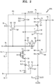
FIG. 2 is an equivalent circuit diagram illustrating a pixel included in the display device ofFIG. 1 according to an exemplary embodiment of the disclosure; -
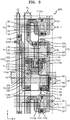
FIG. 3 is a schematic layout diagram illustrating positions of thin-film transistors and a capacitor in the pixel ofFIG. 2 according to an exemplary embodiment of the disclosure; -
FIG. 4 is a schematic layout diagram illustrating a semiconductor layer ofFIG. 3 according to an exemplary embodiment of the disclosure; -
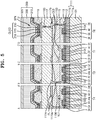
FIG. 5 is a schematic cross-sectional view illustrating a portion ofFIG. 3 according to an exemplary embodiment of the disclosure; -
FIG. 6 is a schematic cross-sectional view illustrating a portion of a display device according to an exemplary embodiment of the disclosure; and -
FIG. 7 is a schematic cross-sectional view illustrating a portion of a display device according to an exemplary embodiment of the disclosure. - Reference will now be made in detail to exemplary embodiments of the present disclosure, examples of which are illustrated in the accompanying drawings. Like reference numerals refer to like elements throughout the drawings and the specification. In this regard, the present invention may have different forms and should not be necessarily construed as being limited to the descriptions set forth herein. Accordingly, several exemplary embodiments are described below, by referring to the figures, to explain aspects of the present description. As used herein, the term "and/or" includes any and all combinations of one or more of the associated listed items. Throughout the disclosure, the expression "at least one of a, b or c" indicates only a, only b, only c, both a and b, both a and c, both b and c, all of a, b, and c, or variations thereof.
- As the present disclosure allows for various changes and numerous embodiments, certain embodiments will be illustrated in the drawings and described in the written description. Effects and features of one or more embodiments and methods of accomplishing the same will become apparent from the following detailed description of the one or more embodiments, taken in conjunction with the accompanying drawings. The disclosure may, however, be embodied in many different forms and is not necessarily limited to the exemplary embodiments set forth herein.
- In the embodiments described below, when a layer, film, region, or plate is referred to as being "on" another layer, film, region, or plate, it can be directly or indirectly on the other layer, film, region, or plate. That is, for example, intervening layers, films, regions, or plates may be present. Sizes of components in the drawings may be exaggerated or reduced for convenience of description. For example, since sizes and thicknesses of components in the drawings may be illustrated for convenience of description, the following embodiments are not necessarily limited thereto.
- In the embodiments described below, when a wire is referred to as "extending in a first direction or a second direction", the wire may extend in a straight shape or may extend in a zigzag or curve along the first direction or the second direction.
- In the embodiments described below, the phrase "in a plan view" refers to a case where a target portion is viewed from above, and the phrase "in a cross-sectional view" refers to a case where a vertical cross-section of a target portion is viewed from the side. In the embodiments described below, when a first component is referred to as "overlapping" a second component, the first component may be arranged above or below the second component. Also, terms like "first" and "third" are used as labels to refer to components of a device without necessarily requiring that device to having a specific number (e.g. three in this example) of such components.
-
FIG. 1 is a schematic conceptual diagram of adisplay device 1 according to an exemplary embodiment of the disclosure. - The
display device 1 according to the present embodiment may be implemented as an electronic device such as a smartphone, a mobile phone, a navigation device, a games console, a television (TV), a vehicle head unit, a notebook computer, a laptop computer, a tablet computer, a personal media player (PMP), personal digital assistants (PDA), etc. Also, the electronic device may be a flexible device. - As shown in
FIG. 1 , thedisplay device 1 according to the present embodiment has a display area DA and a peripheral area PA. The peripheral area PA may surround the display area DA. In an embodiment, the display area DA includes pixels for displaying an image and the peripheral area PA does not include pixels. Thedisplay device 1 may include a substrate 101 (refer toFIG. 5 ), and a shape of thesubstrate 101 is not limited to a rectangular shape (on an xy plane) shown inFIG. 1 and may have various shapes such as a circular shape in other embodiments. Also, thesubstrate 101 may have a bending area and be bent in the bending area. For example, thedisplay device 1 may be bendable. - The
substrate 101 may include glass or metal. Also, thesubstrate 101 may include various flexible or bendable materials. For example, thesubstrate 101 may include a polymer resin such as polyethersulfone, polyacrylate, polyetherimide, polyethylene naphthalate, polyethylene terephthalate, polyphenylene sulfide, polyarylate, polyimide, polycarbonate, or cellulose acetate propionate. - In an exemplary embodiment, the
substrate 101 has a multilayer structure including two layers including the polymer resin described above and a barrier layer including an inorganic material between the two layers. For example, the barrier layer may include silicon oxide, silicon nitride and/or silicon oxynitride. - A plurality of display elements may be arranged in the display area DA. For example, the display element may be an organic light-emitting diode and may emit red, green, blue, or white light. A (sub-)pixel in the display area DA of the
display device 1 ofFIG. 1 includes such an organic light-emitting diode, and also includes a capacitor and a thin film transistor configured to control a degree to which the organic light-emitting diode emits light. - A driver and a wire (or line) such as a power supply wire may be arranged in the peripheral area PA. Also, the peripheral area PA may include a pad area which is an area to which various electronic devices such as a driving integrated circuit (IC) or a printed circuit board is electrically attached. The pad area may include pads (e.g., conductive elements). Various wires for transmitting electrical signals to the display area DA, the printed circuit board, or the driving IC may be attached to the pads.
-
FIG. 2 is an equivalent circuit diagram illustrating a (sub-)pixel in the display area DA of thedisplay device 1 ofFIG. 1 according an exemplary embodiment of the disclosure. The (sub-)pixel may refer to a pixel or a sub-pixel. - Referring to
FIG. 2 , a (sub-)pixel SPX includes an organic light-emitting diode OLED as a display element and a pixel circuit PC (or pixel circuit portion) connected to the organic light-emitting diode OLED. The pixel circuit PC may include a plurality of thin film transistors and a capacitor. For example, the thin film transistors may include first to seventh transistors T1 to T7 and a storage capacitor Cst. According to types (p-type or n-type) and/or operation conditions of transistors, a first terminal of each of the first to seventh transistors T1 to T7 may be a source terminal or a drain terminal, and a second terminal thereof may be different from the first terminal. For example, when the first terminal is a source terminal, the second terminal may be a drain terminal. In an embodiment, the first to seventh transistors T1 to T7 may be implemented by a p-channel multi-oxide semiconductor field effect transistor MOSFET or a p-channel metal oxide semiconductor (PMOS) transistor. - The first transistor T1 may be referred to as a driving transistor. The second transistor T2 may be referred to as a switching transistor. The third transistor T3 may be referred to as a compensation transistor. The fourth transistor T4 may be referred to as a first initialization transistor. The fifth transistor T5 may be referred to as an operation control transistor. The sixth transistor T6 may be referred to as an emission control transistor. The seventh transistor T7 may be referred to as a second initialization transistor. The thin film transistors and the storage capacitor Cst may be connected to signal lines, for example, a scan line SL, a previous scan line SL-1, a next scan
line SL+ 1, an emission control line EL, and a data line DL, a first initialization voltage line VL1, a second initialization voltage line VL2, and a power voltage line PL. - The signal lines, for example, the scan line SL, the previous scan line SL-1, the next scan
line SL+ 1, the emission control line EL, and the data line DL, may include the scan line SL configured to transmit a scan signal Sn, the previous scan line SL-1 configured to transmit a previous scan signal Sn-1 to the first initialization thin film transistor T4, the next scan line SL+1 configured to transmit the scan signal Sn to the second initialization thin film transistor T7, the emission control line EL configured to transmit an emission control signal En to the operation control thin film transistor T5 and the emission control thin film transistor T6, and the data line DL crossing the scan line SL and configured to transmit a data signal Dm. The power voltage line PL may be configured to transmit a driving voltage ELVDD to the driving thin film transistor T1. The first initialization voltage line VL1 may be configured to transmit an initialization voltage Vint to the first initialization thin film transistor T4. The second initialization voltage line VL2 may be configured to transmit the initialization voltage Vint to the second initialization thin film transistor T7. As shown inFIGS. 2 and3 , the first initialization voltage line VL1 and the second initialization voltage line VL2 may appear as a same wire, i.e., an initialization voltage line VL. Specifically,FIG. 3 shows the layout diagram of the pixel in nth row, and the first initialization voltage line VL1 in nth row may be the second initialization voltage line VL2 in n-1th row. - A driving gate electrode G1 of the driving thin film transistor T1, is connected to a lower electrode CE1 of the storage capacitor Cst. A driving source region S1 of the driving thin film transistor T1 is connected to the power voltage line PL via the operation control thin film transistor T5. A driving drain region D1 of the driving thin film transistor T1 is electrically connected to a pixel electrode of an organic light-emitting diode OLED via the emission control thin film transistor T6. That is, in response to a voltage applied to a first node N1 (e.g., a voltage applied to the driving gate electrode G1), the driving thin film transistor T1 may control an amount of current flowing from a second node N2 connected to the power voltage line PL to the organic light-emitting diode OLED. Accordingly, the driving thin film transistor T1 receives the data signal Dm according to a switching operation of the switching thin film transistor T2 and supplies a driving current IOLED to the organic light-emitting diode OLED. The operation control thin film transistor T5 may be interposed between the second node N2 and the power voltage line PL.
- A switching gate electrode G2 of the switching thin film transistor T2, is connected to the scan line SL. A switching source region S2 of the switching thin film transistor T2 is connected to the data line DL. A switching drain region D2 of the switching thin film transistor T2 is connected to the second node N2 and thus connected to the driving source region S1 of the driving thin film transistor T1 and is also connected to the power voltage line PL via the operation control thin film transistor T5. The switching thin film transistor T2 is turned on according to the scan signal Sn received through the scan line SL to perform a switching operation for transmitting the data signal Dm transmitted through the data line DL to the driving source region S1 of the driving thin film transistor T1.
- The compensation thin film transistor T3, may be connected between a third node N3 between the driving thin film transistor T1 and the organic light-emitting diode OLED and the first node N1 to diode-connect the driving thin film transistor T1 in response to a voltage applied to a compensation gate electrode G3 of the compensation thin film transistor T3. The compensation gate electrode G3 of the compensation thin film transistor T3 is connected to the scan line SL. A compensation source region S3 of the compensation thin film transistor T3 is connected to the driving drain region D1 of the driving thin film transistor T1 and is also connected to the pixel electrode of the organic light-emitting diode OLED via the emission control thin film transistor T6. A compensation drain region D3 of the compensation thin film transistor T3 is connected to the lower electrode CE1 of the storage capacitor Cst, a first initialization drain region D4 of the first initialization thin film transistor T4, and the driving gate electrode G1 of the driving thin film transistor T1. The compensation thin film transistor T3 is turned on according to the scan signal Sn received through the scan line SL to electrically connect the driving gate electrode G1 and the driving drain region D1 of the driving thin film transistor T1 and diode-connect the driving thin film transistor T1.
- The first initialization thin film transistor T4, may be connected between the first node N1 and the first initialization voltage line VL1 to initialize a voltage of the driving gate electrode G1 in response to a voltage applied to a first initialization gate electrode G4. The first initialization gate electrode G4 of the first initialization thin film transistor T4 is connected to the previous scan line SL-1. A first initialization source region S4 of the first initialization thin film transistor T4 is connected to the first initialization voltage line VL1. The first initialization drain region D4 of the first initialization thin film transistor T4 is connected to the lower electrode CE1 of the storage capacitor Cst, the compensation drain region D3 of the compensation thin film transistor T3, and the driving gate electrode G1 of the driving thin film transistor T1. The first initialization thin film transistor T4 is turned on according to the previous scan signal Sn-1 received through the previous scan line SL-1 to perform an initialization operation for initializing a voltage of the driving gate electrode G1 of the driving thin film transistor T1 by transmitting the initialization voltage Vint to the driving gate electrode G1 of the driving thin film transistor T1.
- The operation control thin film transistor T5 may be connected between the second node N2 and the power voltage line PL and be turned on in response to a voltage applied to an operation control gate electrode G5. The operation control gate electrode G5 of the operation control thin film transistor T5 is connected to the emission control line EL. An operation control source region S5 of the operation control thin film transistor T5 is connected to the power voltage line PL. An operation control drain region D5 of the operation control thin film transistor T5 is connected to the driving source region S1 of the driving thin film transistor T1 and the switching drain region D2 of the switching thin film transistor T2.
- The emission control thin film transistor T6 may be connected between the third node N3 and the organic light-emitting diode OLED and be turned on in response to a voltage applied to an emission control gate electrode G6, from the emission control line EL. The emission control gate electrode G6 of the emission control thin film transistor T6 is connected to the emission control line EL. An emission control source region S6 of the emission control thin film transistor T6 is connected to the driving drain region D1 of the driving thin film transistor T1 and the compensation source region S3 of the compensation thin film transistor T3. An emission control drain region D6 of the emission control thin film transistor T6 is electrically connected to a second initialization source region S7 of the second initialization thin film transistor T7 and the pixel electrode of the organic light-emitting diode OLED.
- When the operation control thin film transistor T5 and the emission control thin film transistor T6 are simultaneously turned on (or turned on during a same period) according to the emission control signal En received through the emission control line EL, the driving voltage ELVDD is transmitted to the organic light-emitting diode OLED so that the driving current IOLED flows through the organic light-emitting diode OLED.
- A second initialization gate electrode G7 of the second initialization thin film transistor T7, is connected to the next scan
line SL+ 1. The second initialization source region S7 of the second initialization thin film transistor T7 is connected to the emission control drain region D6 of the emission control thin film transistor T6 and the pixel electrode of the organic light-emitting diode OLED. A second initialization drain region D7 of the second initialization thin film transistor T7 is connected to the second initialization voltage line VL2. - In an embodiment where the scan line SL and the next scan line SL+1 are electrically connected to each other, the same scan signal Sn is applied to the scan line SL and the next scan
line SL+ 1. Accordingly, the second initialization thin film transistor T7 may be turned on according to the scan signal Sn received through the next scan line SL+1 to perform an operation of initializing the pixel electrode of the organic light-emitting diode OLED. In an exemplary embodiment, the second initialization thin film transistor T7 is omitted. - An upper electrode CE2 of the storage capacitor Cst is connected to the power voltage line PL, and a common electrode of the organic light-emitting diode OLED is connected to a common voltage ELVSS. Accordingly, the organic light-emitting diode OLED may receive the driving current IOLED from the driving thin film transistor T1 and emit light, thereby displaying an image. In an exemplary embodiment, the common voltage ELVSS is less than the driving voltage ELVDD.
- Although
FIG. 2 shows the compensation thin film transistor T3 and the first initialization thin film transistor T4 having dual gate electrodes, the compensation thin film transistor T3 and the first initialization thin film transistor T4 may have one gate electrode in other embodiments. -
FIG. 3 is a schematic layout diagram illustrating positions of a plurality of thin film transistors and a capacitor in the (sub-)pixel ofFIG. 2 according to an exemplary embodiment of the disclosure.FIG. 4 is a schematic layout diagram of asemiconductor layer 1130, which is a portion of the display device ofFIG. 3 .FIG. 5 is a cross-sectional view of a portion ofFIG. 3 , taken along lines A-A', B-B', C-C', and D-D'. The size of each component in the cross-sectional view has been exaggerated and/or reduced for convenience. This also applies to the cross-sectional views described below. - The driving thin film transistor T1, the switching thin film transistor T2, the compensation thin film transistor T3, the first initialization thin film transistor T4, the operation control thin film transistor T5, the emission control thin film transistor T6, and the second initialization thin film transistor T7 are arranged along the
semiconductor layer 1130. Some areas of thesemiconductor layer 1130 may constitute semiconductor layers of the driving thin film transistor T1, the switching thin film transistor T2, the compensation thin film transistor T3, the first initialization thin film transistor T4, the operation control thin film transistor T5, the emission control thin film transistor T6, and the second initialization thin film transistor T7. That is, some areas of thesemiconductor layer 1130 may constitute an active region, a source region, or a drain region of a thin film transistor. - The
semiconductor layer 1130 may be on thesubstrate 101. A buffer layer 111 may be on thesubstrate 101, and thesemiconductor layer 1130 may be on the buffer layer 111. - The buffer layer 111 may reduce or prevent penetration of foreign materials, moisture, or external air from the bottom of the
substrate 101 and may provide a flat surface on thesubstrate 101. The buffer layer 111 may include an inorganic material such as oxide or nitride, an organic material, or an organic-inorganic complex material and may have a single-layer or multilayer structure of an inorganic material and an organic material. For example, the buffer layer 111 may have a structure in which a first buffer layer 111a and asecond buffer layer 111b are stacked, and the first buffer layer 111a and thesecond buffer layer 111b may include different materials from each other. For example, the first buffer layer 111a may include silicon nitride, and thesecond buffer layer 111b may include silicon oxide. - As described above, in an embodiment where the first buffer layer 111a includes a silicon nitride material, the silicon nitride material includes hydrogen. Accordingly, carrier mobility of the
semiconductor layer 1130 arranged on the buffer layer 111 may improve, and thus, electrical characteristics of the thin film transistor may improve. In an embodiment, thesemiconductor layer 1130 may include a silicon material. In this embodiment, interface bonding characteristics between thesemiconductor layer 1130 including silicon and thesecond buffer layer 111b including silicon oxide may improve, and thus, electrical characteristics of the thin film transistor may improve. - The
semiconductor layer 1130 may include low temperature polysilicon or a Low Temperature Polycrystalline Silicon (LTPS). The polysilicon material has high electron mobility (100 cm2/Vs or greater) and thus has low energy consumption and excellent reliability. As another example, thesemiconductor layer 1130 may include amorphous silicon (a-Si) and/or an oxide semiconductor. Alternatively, some semiconductor layers of the plurality of thin film transistors may include LTPS, and some of the other semiconductor layers may include a-Si and/or an oxide semiconductor. - Source regions and drain regions of the
semiconductor layer 1130 may be doped with impurities, and the impurities may include N-type impurities or P-type impurities. The source region and the drain region may correspond to a source electrode and a drain electrode, respectively. The source region and the drain region may be exchanged with each other according to properties of the thin film transistor. Hereinafter, the terms "source region" and "drain region" are used instead of the source electrode and the drain electrode. The equivalent circuit diagram ofFIG. 2 shows certain portions of thesemiconductor layer 1130 doped with P-type impurities to implement the thin film transistors as a p-channel metal-oxide semiconductor field effect transistors (MOSFETs) or p-channel metal oxide semiconductor (PMOS) transistors. Other portions of thesemiconductor layer 1130 may also be doped with impurities to serve as wires configured to electrically connect the thin film transistors and/or the capacitor to each other. - A first
gate insulating layer 112 may be arranged on thesemiconductor layer 1130, and the driving gate electrode G1, the scan line SL, the previous scan line SL-1, the next scanline SL+ 1, and the emission control line EL may be arranged on the firstgate insulating layer 112. The firstgate insulating layer 112 may be disposed on the buffer layer 111. The firstgate insulating layer 112 may include silicon oxide (SiO2), silicon nitride (SiNx), silicon oxynitride (SiON), aluminum oxide (Al2O3), titanium oxide (TiO2), tantalum oxide (Ta2O5), hafnium oxide (HfO2), or zinc oxide (ZnO). - Areas of the scan line SL overlapping second and third active regions A2 and A3 of the switching and compensation thin film transistors T2 and T3 may be the switching and compensation gate electrodes G2 and G3, respectively. An area of the previous scan line SL-1 overlapping a fourth active region A4 of the first initialization thin film transistor T4 may be the first initialization gate electrode G4. An area of the next scan line SL+1 overlapping a seventh active region A7 (e.g., a second initialization active region) of the second initialization thin film transistor T7 may be the second initialization gate electrode G7. Areas of the emission control line EL overlapping fifth and sixth active regions A5 and A6 of the operation control and emission control thin film transistors T5 and T6 may be the operation control and emission control gate electrodes G5 and G6, respectively.
- The driving gate electrode G1, the scan line SL, the previous scan line SL-1, the next scan
line SL+ 1, and the emission control line EL may include a conductive material including molybdenum (Mo), aluminum (Al), copper (Cu), or titanium (Ti) and may have a multilayer or single-layer structure including the material described above. For example, the driving gate electrode G1, the scan line SL, the previous scan line SL-1, the next scanline SL+ 1, and the emission control line EL may have a multilayer structure of Mo/AI or may have a multilayer structure of Mo/AI/Mo. - A second
gate insulating layer 113 may be arranged on the driving gate electrode G1, the scan line SL, the previous scan line SL-1, the next scanline SL+ 1, and the emission control line EL. The secondgate insulating layer 113 may be disposed on the firstgate insulating layer 112. The secondgate insulating layer 113 may include silicon oxide (SiO2), silicon nitride (SiNx), silicon oxynitride (SiON), aluminum oxide (Al2O3), titanium oxide (TiO2), tantalum oxide (Ta2O5), hafnium oxide (HfO2), or zinc oxide (ZnO). - An electrode voltage line HL, the first initialization voltage line VL1, and the second initialization voltage line VL2 may be arranged on the second
gate insulating layer 113. The electrode voltage line HL may cover at least a portion of the driving gate electrode G1 and may constitute the storage capacitor Cst together with the driving gate electrode G1. In an exemplary embodiment, the electrode voltage line HL entirely covers the driving gate electrode G1. - The lower electrode CE1 of the storage capacitor Cst may be integrally formed with the driving gate electrode G1 of the driving thin film transistor T1. For example, the driving gate electrode G1 of the driving thin film transistor T1 may serve as the lower electrode CE1 of the storage capacitor Cst. An area of the electrode voltage line HL overlapping the driving gate electrode G1 may be the upper electrode CE2 of the storage capacitor Cst. Accordingly, the second
gate insulating layer 113 may serve as a dielectric layer of the storage capacitor Cst. - The electrode voltage line HL, the first initialization voltage line VL1, and the second initialization voltage line VL2 may include a conductive material including molybdenum (Mo), aluminum (Al), copper (Cu), or titanium (Ti) and may have a multilayer or single-layer structure including the material described above. For example, the electrode voltage line HL, the first initialization voltage line VL1, and the second initialization voltage line VL2 may have a multilayer structure of Mo/AI or may have a multilayer structure of Mo/AI/Mo.
- An interlayer insulating
layer 115 is arranged on the electrode voltage line HL, the first initialization voltage line VL1, and the second initialization voltage line VL2. The interlayer insulatinglayer 115 may be disposed on the secondgate insulating layer 113. The interlayer insulatinglayer 115 may include silicon oxide (SiO2), silicon nitride (SiNx), silicon oxynitride (SiON), aluminum oxide (Al2O3), titanium oxide (TiO2), tantalum oxide (Ta2O5), hafnium oxide (HfO2), or zinc oxide (ZnO). - The data line DL, the power voltage line PL, first and second
initialization connection lines node connection line 1174, and aconnection metal 1175 may be arranged on theinterlayer insulating layer 115. The data line DL, the power voltage line PL, thenode connection line 1174, and theconnection metal 1175 may include a conductive material including molybdenum (Mo), aluminum (Al), copper (Cu), or titanium (Ti) and may have a multilayer or single-layer structure including the material described above. For example, the data line DL, the power voltage line PL, thenode connection line 1174, and theconnection metal 1175 may have a multilayer structure of Ti/Al/Ti. - The data line DL may be connected to the switching source region S2 of the switching thin film transistor T2 through a
contact hole 1154. A portion of the data line DL may correspond to the switching source region S2. - The power voltage line PL may be connected to the upper electrode CE2 of the storage capacitor Cst through a contact hole 1158 formed in the
interlayer insulating layer 115. Accordingly, the electrode voltage line HL may have the same voltage level (a constant voltage) as the power voltage line PL. Also, the power voltage line PL may be connected to the operation control source region S5 through acontact hole 1155. - The first initialization voltage line VL1 may be connected to the first initialization thin film transistor T4 through the first
initialization connection line 1173a, and the second initialization voltage line VL2 may be connected to the second initialization thin film transistor T7 through the secondinitialization connection line 1173b. The first initialization voltage line VL1 and the second initialization voltage line VL2 may have the same constant voltage (for example, -2 V, etc.). - In an exemplary embodiment, one end of the
node connection line 1174 is connected to the compensation drain electrode D3 through acontact hole 1156, and the other end is connected to the driving gate electrode G1 through acontact hole 1157. - The
connection metal 1175 is connected to the sixth active region A6 of the emission control thin film transistor T6 through acontact hole 1153 passing through (e.g., penetrates) theinterlayer insulating layer 115, the secondgate insulating layer 113, and the firstgate insulating layer 112. Theconnection metal 1175 is connected to apixel electrode 210 of the organic light-emitting diode OLED through acontact hole 1163. Accordingly, the emission control thin film transistor T6 may be electrically connected to thepixel electrode 210 of the organic light-emitting diode OLED. - A
planarization layer 117 may be arranged on the data line DL, the power voltage line PL, the first and secondinitialization connection lines node connection line 1174, and theconnection metal 1175. The organic light-emitting diode OLED may be arranged on theplanarization layer 117. - Although
FIG. 2 shows one pixel circuit PC, andFIG. 3 shows a structure of one (sub-)pixel SPX, a plurality of sub-pixels SPX having the same pixel circuit PC may be arranged in a first direction (x-axis direction) and a second direction (y-axis direction). A plurality of sub-pixels SPX may share lines. For example, the first initialization voltage line VL1, the previous scan line SL-1, the second initialization voltage line VL2, and the next scan line SL+1 may be shared by two pixel circuits PC adjacent to each other in the second direction (y-axis direction). - That is, the first initialization voltage line VL1 and the previous scan line SL-1 may be electrically connected to a second initialization thin film transistor of another pixel circuit PC arranged above (direction +y) the pixel circuit PC of
FIG. 3 in the second direction (y-axis direction) based on the drawing. Accordingly, a previous scan signal applied to the previous scan line SL-1 may be transmitted to the second initialization thin film transistor of the other pixel circuit PC as a next scan signal. In the same manner, the second initialization voltage line VL2 and the next scan line SL+1 may be electrically connected to a first initialization thin film transistor of another adjacent pixel circuit PC arranged below (direction -y) the pixel circuit PC ofFIG. 3 in the second direction (y-axis direction) based on the drawing and thus may transmit a previous scan signal and an initialization voltage to the first initialization thin film transistor of the other pixel circuit PC. - Referring back to
FIG. 5 , theplanarization layer 117 may have a flat upper surface so that thepixel electrode 210 may be flat. Theplanarization layer 117 may include an organic material and may have a single-layer or multilayer structure. Theplanarization layer 117 may include a general commercial polymer such as benzocyclobutene (BCB), polyimide, hexamethyldisiloxane (HMDSO), poly(methyl methacrylate) (PMMA), or polystyrene (PS), a polymer derivative having a phenol-based group, an acryl-based polymer, an imide-based polymer, an aryl ether-based polymer, an amide-based polymer, a fluorine-based polymer, a p-xylene-based polymer, a vinyl alcohol-based polymer, or a blend thereof. In an exemplary embodiment, theplanarization layer 117 includes an inorganic material. Theplanarization layer 117 may include silicon oxide (SiO2), silicon nitride (SiNx), silicon oxynitride (SiON), aluminum oxide (Al2O3), titanium oxide (TiO2), tantalum oxide (Ta2O5), hafnium oxide (HfO2), or zinc oxide (ZnO). When theplanarization layer 117 includes an inorganic material, chemical planarization polishing may be performed in some embodiments. In some embodiments, theplanarization layer 117 may include both of an organic material and an inorganic material. - The organic light-emitting diode OLED may include the
pixel electrode 210, acommon electrode 230, and anintermediate layer 220 interposed between thepixel electrode 210 and thecommon electrode 230 and including an emission layer. - The
pixel electrode 210 may be connected to theconnection metal 1175 through thecontact hole 1163, and theconnection metal 1175 may be connected to the emission control drain region D6 through thecontact hole 1153. Thepixel electrode 210 may be a (semi)transmissive electrode or a reflective electrode. In some embodiments, thepixel electrode 210 may include a reflective film including Ag, Mg, Al, Pt, Pd, Au, Ni, Nd, Ir, Cr, and a compound thereof and a transparent or semitransparent electrode layer disposed on the reflective film. The transparent or semitransparent electrode layer may include at least one selected from the group including indium tin oxide (ITO), indium zinc oxide (IZO), zinc oxide (ZnO), indium oxide (In2O3), indium gallium oxide (IGO), and aluminum zinc oxide (AZO). In some embodiments, thepixel electrode 210 may have a stack structure of ITO/Ag/ITO. - A pixel-defining
layer 119 may be arranged on theplanarization layer 117, and the pixel-defininglayer 119 may have an opening portion exposing a center portion of thepixel electrode 210. Thus, the pixel-defininglayer 119 may define an emission area of a pixel. Also, the pixel-defininglayer 119 may prevent an arc from occurring at the edge of thepixel electrode 210 by increasing a distance between an edge of thepixel electrode 210 and thecommon electrode 230 arranged over thepixel electrode 210. The pixel-defininglayer 119 may be formed by a method such as spin coating, using an organic insulating material such as polyimide, polyamide, acrylic resin, BCB, HMDSO, or phenol resin. - The
intermediate layer 220 may include an organic emission layer. The organic emission layer may include an organic material including a fluorescent or phosphorescent material that emits red, green, blue, or white light. The organic emission layer may include a low-molecular weight organic material or a polymer organic material, and functional layers such as a hole transport layer (HTL), a hole injection layer (HIL), an electron transport layer (ETL), and an electron injection layer (EIL) may be selectively further arranged under and on the organic emission layer. Theintermediate layer 220 may correspond to each of a plurality ofpixel electrodes 210. However, embodiments of the disclosure are not limited thereto, and a layer such as an HTL, an HIL, an ETL, or an EIL from among layers included in theintermediate layer 220 may be integrally formed over the plurality ofpixel electrodes 210. - The
common electrode 230 may be a transmissive electrode or a reflective electrode. In an embodiment, thecommon electrode 230 may be a transparent or semitransparent electrode and may include a metal thin film having a low work function and including Li, Ca, LiF/Ca, LiF/AI, Al, Ag, Mg, and a compound thereof. In addition to the metal thin film, thecommon electrode 230 may further include a transparent conductive oxide (TCO) film such as ITO, IZO, ZnO, or In2O3. Thecommon electrode 230 may be integrally formed to correspond to the plurality ofpixel electrodes 210. - An
encapsulation layer 300 including a firstinorganic encapsulation layer 310, a secondinorganic encapsulation layer 320, and anorganic encapsulation layer 330 therebetween may be arranged on thecommon electrode 230. - The first
inorganic encapsulation layer 310 and the secondinorganic encapsulation layer 320 may include silicon oxide (SiO2), silicon nitride (SiNx), silicon oxynitride (SiON), aluminum oxide (Al2O3), titanium oxide (TiO2), tantalum oxide (Ta2O5), hafnium oxide (HfO2), or zinc oxide (ZnO). Theorganic encapsulation layer 330 may include polyethylene terephthalate, polyethylene naphthalate, polycarbonate, polyimide, polyethylene sulfonate, polyoxymethylene, polyarylate, HMDSO, acrylic resin (for example, PMMA, polyacrylic acid, etc.), or any combination thereof. - As described above, the first
gate insulating layer 112 may be arranged on thesemiconductor layer 1130, and the driving gate electrode G1, the scan line SL, the previous scan line SL-1, the next scanline SL+ 1, and the emission control line EL may be arranged on the firstgate insulating layer 112. The scan line SL, the previous scan line SL-1, the next scanline SL+ 1, and the emission control line EL, as described above, include the switching gate electrode G2, the compensation gate electrode G3, the first initialization gate electrode G4, the operation control gate electrode G5, the emission control gate electrode G6, and the second initialization gate electrode G7. Accordingly, the firstgate insulating layer 112 is interposed between the driving gate electrode G1, the switching gate electrode G2, the compensation gate electrode G3, the first initialization gate electrode G4, the operation control gate electrode G5, the emission control gate electrode G6, and the second initialization gate electrode G7 and thesemiconductor layer 1130. - In an organic light-emitting display device according to an exemplary embodiment of the disclosure, a dielectric constant in a
first portion 1121 of the firstgate insulating layer 112 between the first active region A1 (e.g., a driving active region) and the driving gate electrode G1 is greater than a dielectric constant in asecond portion 1122 of the firstgate insulating layer 112 between the third active region A3 (e.g., a compensation active region) and the compensation gate electrode G3. - As described above with reference to
FIG. 2 , the driving thin film transistor T1 receives the data signal Dm according to a switching operation of the switching thin film transistor T2 and supplies the driving current IOLED to the organic light-emitting diode OLED. That is, a voltage between the driving gate electrode G1 and the driving source region S1 of the driving thin film transistor T1 determines the driving current IOLED flowing through the organic light-emitting diode OLED. In this regard, when threshold voltages Vth of driving thin film transistors T1 of several pixels are different from each other, sizes of driving currents IOLED flowing through organic light-emitting diodes OLED are different from each other even if the same data signal Dm is applied to those several pixels. A display device may be unable to display a high-quality image when the sizes of the driving currents IOLED flowing through organic light-emitting diodes are different from each other while the same data signal Dm is applied to those several pixels. - The compensation thin film transistor T3 may be connected to each of the driving thin film transistors T1 to prevent the influence of the threshold voltages Vth in the driving thin film transistors T1. Thus, even if the threshold voltages Vth of the driving thin film transistors T1 of several pixels are different from each other, sizes of the driving currents IOLED flowing through the organic light-emitting diodes OLED may be almost the same as each other when the same data signal Dm is applied to those several pixels.
- However, even with the compensation thin film transistor T3, the pixels may be unable to display a high-quality image. After compensating for a threshold voltage Vth in a voltage difference between the driving gate electrode G1 and the driving source region S1 of the driving thin film transistor T1, the compensation thin film transistor T3 is completely turned off to prevent a current flowing in a direction from the driving thin film transistor T1 to the organic light-emitting diode OLED from flowing to the compensation thin film transistor T3 at the third node N3. However, even when the compensation thin film transistor T3 is turned off, a leakage current flowing from the compensation source region S3 of the compensation thin film transistor T3 to the compensation drain region D3 exists. When sizes of such leakage currents are different from each other in the compensation thin film transistors T3, sizes of the driving currents IOLED flowing through the organic light-emitting diodes OLED are different from each other even if the same data signal Dm is applied to several pixels. A display device may be unable to display a high-quality image when the sizes of the driving currents IOLED flowing through the organic light-emitting diodes OLED are different from each other while the same data signal Dm is applied to several pixels.
- Furthermore, a parasitic capacitance may exist between the third active region A3 and the compensation gate electrode G3 of the compensation thin film transistor T3, thereby resulting in a kick-back phenomenon occurring in the display device. The kick-back phenomenon refers to a flicker phenomenon in which a screen of the display device flickers, or a phenomenon that a residual image remains on the screen.
- However, in an organic light-emitting display device according to at least one exemplary embodiment of the disclosure, a dielectric constant in the
first portion 1121 of the firstgate insulating layer 112 between the first active region A1 and the driving gate electrode G1 is greater than a dielectric constant in thesecond portion 1122 of the firstgate insulating layer 112 between the third active region A3 and the compensation gate electrode G3. That is, a dielectric constant in thesecond portion 1122 of the firstgate insulating layer 112 between the third active region A3 and the compensation gate electrode G3 is less than a dielectric constant in thefirst portion 1121 of the firstgate insulating layer 112 between the first active region A1 and the driving gate electrode G1. - When a dielectric constant in the
second portion 1122 of the firstgate insulating layer 112 between the third active region A3 and the compensation gate electrode G3 decreases, a parasitic capacitance between the third active region A3 and the compensation gate electrode G3 may decrease, and thus, the kick-back phenomenon may be prevented or reduced, and a size of leakage current in the compensation thin film transistor T3 may decrease. When sizes of leakage currents in the compensation thin film transistors T3 decrease, a difference in the sizes of leakage currents in the compensation thin film transistors T3 also decreases. Accordingly, a display device according to at least one exemplary embodiment of the disclosure may display a high-quality image. - In an exemplary embodiment, a dielectric constant in a
fourth portion 1124 of the firstgate insulating layer 112 between the sixth active region A6 and the emission control gate electrode G6 is the same as a dielectric constant in thefirst portion 1121 of the firstgate insulating layer 112 between the first active region A1 and the driving gate electrode G1. This also applies to the embodiments described later and modifications thereof. - As shown in
FIG. 5 , thesecond portion 1122 of the firstgate insulating layer 112 between the third active region A3 and the compensation gate electrode G3 may be a portion where the compensation gate electrode G3 and the third active region A3 overlap each other. When the compensation gate electrode G3 and the third active region A3 are referred to as overlapping each other, it means that the compensation gate electrode G3 and the third active region A3 overlap each other when viewed from a direction perpendicular to thesubstrate 101 or a direction perpendicular to an upper surface of the compensation gate electrode G3. As shown inFIGS. 3 to 5 , when the compensation thin film transistor T3 has dual gate electrodes, the firstgate insulating layer 112 may have twosecond portions 1122 spaced apart from each other in the compensation thin film transistor T3. - As described above, parasitic capacitance in the compensation thin film transistor T3 occurs between the compensation gate electrode G3 and the third active region A3. Accordingly, when viewed from a direction perpendicular to the
substrate 101 or a direction perpendicular to an upper surface of the compensation gate electrode G3, an area of thesecond portion 1122 having a lower dielectric constant than thefirst portion 1121 in the firstgate insulating layer 112 may be at least the same as an area of a portion of the compensation gate electrode G3 overlapping the third active region A3. - In two components arranged on different layers, parasitic capacitance does not only occur between portions of the components overlapping each other in a direction perpendicular to the
substrate 101. Accordingly, to reduce parasitic capacitance, as shown inFIG. 6 , which is a schematic cross-sectional view of a portion of a display device according to an exemplary embodiment, when viewed from a direction perpendicular to thesubstrate 101 or a direction perpendicular to an upper surface of the compensation gate electrode G3, an area of thesecond portion 1122 having a lower dielectric constant than thefirst portion 1121 in the firstgate insulating layer 112 is larger than an area of a portion of the compensation gate electrode G3 overlapping the third active region A3. - Furthermore, as shown in
FIG. 7 , which is a schematic cross-sectional view of a portion of a display device according to exemplary embodiment, in the compensation thin film transistor T3 having dual gate electrodes, thesecond portion 1122 having a lower dielectric constant than thefirst portion 1121 in the firstgate insulating layer 112 may correspond to not only compensation gate electrodes G3 spaced apart from each other but also a portion between the compensation gate electrodes G3 (i.e., a region A3a between two third active regions A3). - Thus, a kick-back phenomenon in the compensation thin film transistor T3 may be prevented or reduced, and a size of leakage current in the compensation thin film transistor T3 may decrease. When sizes of leakage currents in the compensation thin film transistors T3 decrease, a difference in the sizes of leakage currents in the compensation thin film transistors T3 also decreases. Accordingly, a display device according to at least one exemplary embodiment of the disclosure may display a high-quality image.
- In an exemplary embodiment of the disclosure, a dielectric constant in the
second portion 1122 of the firstgate insulating layer 112 between the third active region A3 and the compensation gate electrode G3 is less than that in thefirst portion 1121 of the firstgate insulating layer 112 between the first active region A1 and the driving gate electrode G1 through various methods. - When the first
gate insulating layer 112 includes silicon oxide, the number of oxygen atoms per unit volume in thesecond portion 1122 may be greater than the number of oxygen atoms per unit volume in thefirst portion 1121 so that a dielectric constant in thesecond portion 1122 is less than that in thefirst portion 1121. Silicon oxide may be denoted as SiOx, where x is the number of oxygen atoms per silicon atom. When x is 1.6 to 1.8 in SiOx, a dielectric constant of silicon oxide is 4.6 to 4.7. When x is 1.9 to 2.0 in SiOx, a dielectric constant of silicon oxide is 4.0 or less. Accordingly, as the number of oxygen atoms per unit volume in a silicon oxide layer increases, a dielectric constant of the silicon oxide layer decreases, and as a result, a size of parasitic capacitance may be reduced. The reason why a dielectric constant of a silicon oxide layer decreases as the number of oxygen atoms per unit volume in the silicon oxide layer increases is that binding energy increases and a polarization phenomenon due to an electric field decreases as an amount of oxygen increases. - When the first
gate insulating layer 112 includes silicon oxide, thesecond portion 1122 may include fluorine or carbon so that a dielectric constant in thesecond portion 1122 is less than that in thefirst portion 1121. That is, thefirst portion 1121 of the firstgate insulating layer 112 may include SiOx, and thesecond portion 1122 may include SiOF or SiOC. In the case of SiO2, the dielectric constant is about 4.2, whereas, in the case of SiOF or SiOC, if the atomic percent of F or C is 3.1, the dielectric constant is 3.8, if the atomic percent of F or C is 7.0, the dielectric constant is 3.4, and if the atomic percent of F or C is 10.0, the dielectric constant is 3.3. Accordingly, when the firstgate insulating layer 112 includes silicon oxide, thesecond portion 1122 may include fluorine or carbon so that a dielectric constant in thesecond portion 1122 is less than the dielectric constant in thefirst portion 1121. - While the driving thin film transistor T1 and the compensation thin film transistor T3 have been mainly described, the above descriptions may be applied to the first initialization thin film transistor T4 in addition to the compensation thin film transistor T3.
- The first initialization thin film transistor T4 initializes a voltage of the driving gate electrode G1 of the driving thin film transistor T1. However, since a leakage current exists in the first initialization thin film transistor T4 after the first initialization thin film transistor T4 is turned off, a voltage of the driving gate electrode G1 of the driving thin film transistor T1 may vary unintentionally. Particularly, when sizes of leakage currents of first initialization thin film transistors T4 are different from each other in a plurality of pixels, degrees to which voltages of driving gate electrodes G1 vary are different from each other in the plurality of pixels. This eventually causes quality degradation of an image displayed by a display device.
- In an exemplary embodiment, a dielectric constant in the
first portion 1121 of the firstgate insulating layer 112 between the first active region A1 and the driving gate electrode G1 is greater than a dielectric constant in athird portion 1123 of the firstgate insulating layer 112 between the fourth active region A4 (e.g., an initialization region) and the first initialization gate electrode G4, to prevent the quality degradation of the image. That is, a dielectric constant in thethird portion 1123 of the firstgate insulating layer 112 between the fourth active region A4 and the first initialization gate electrode G4 may be less than a dielectric constant in thefirst portion 1121 of the firstgate insulating layer 112 between the first active region A1 and the driving gate electrode G1. - When a dielectric constant in the
third portion 1123 of the firstgate insulating layer 112 between the fourth active region A4 and the first initialization gate electrode G4 decreases, a parasitic capacitance between the fourth active region A4 and the first initialization gate electrode G4 may decrease, and thus, a size of leakage current in the first initialization thin film transistor T4 may decrease. When sizes of leakage currents in the first initialization thin film transistors T4 decrease, a difference in the sizes of leakage currents in the first initialization thin film transistors T4 also decreases. Accordingly, a display device according to at least one exemplary embodiment may display a high-quality image. - As shown in
FIG. 5 , thethird portion 1123 of the firstgate insulating layer 112 between the fourth active region A4 and the first initialization gate electrode G4 may be a portion where the first initialization gate electrode G4 and the fourth active region A4 overlap each other. When the first initialization gate electrode G4 and the fourth active region A4 are referred to as overlapping each other, it means that the first initialization gate electrode G4 and the fourth active region A4 overlap each other when viewed from a direction perpendicular to thesubstrate 101 or a direction perpendicular to an upper surface of the first initialization gate electrode G4. As shown inFIGS. 3 to 5 , when the first initialization thin film transistor T4 has dual gate electrodes, the firstgate insulating layer 112 may have twothird portions 1123 spaced apart from each other in the first initialization thin film transistor T4. - As described above, parasitic capacitance in the first initialization thin film transistor T4 occurs between the first initialization gate electrode G4 and the fourth active region A4. Accordingly, when viewed from a direction perpendicular to the
substrate 101 or a direction perpendicular to an upper surface of the first initialization gate electrode G4, an area of thethird portion 1123 having a lower dielectric constant than thefirst portion 1121 in the firstgate insulating layer 112 is at least the same as an area of a portion of the first initialization gate electrode G4 overlapping the fourth active region A4. - In two components arranged on different layers, parasitic capacitance does not only occur between portions of the components overlapping each other in a direction perpendicular to the
substrate 101. Accordingly, to reduce parasitic capacitance, as shown inFIG. 6 , which is a schematic cross-sectional view of a portion of a display device according to an exemplary embodiment, when viewed from a direction perpendicular to thesubstrate 101 or a direction perpendicular to an upper surface of the first initialization gate electrode G4, an area of thethird portion 1123 having a lower dielectric constant than thefirst portion 1121 in the firstgate insulating layer 112 is larger than an area of a portion of the first initialization gate electrode G4 overlapping the fourth active region A4. - Furthermore, as shown in
FIG. 7 , which is a schematic cross-sectional view of a portion of a display device according to an exemplary embodiment, in the first initialization thin film transistor T4 having dual gate electrodes, thethird portion 1123 having a lower dielectric constant than thefirst portion 1121 in the firstgate insulating layer 112 may correspond to not only first initialization gate electrodes G4 spaced apart from each other but also a portion between the first initialization gate electrodes G4 (i.e., a region A4a between two fourth active regions A4). - Thus, a size of leakage current in the first initialization thin film transistor T4 may decrease. When sizes of leakage currents in the first initialization thin film transistors T4 decrease, a difference in the sizes of leakage currents in the first initialization thin film transistors T4 also decreases. Accordingly, a display device according to at least one exemplary embodiment may display a high-quality image.
- In an exemplary embodiment, a dielectric constant in the
third portion 1123 of the firstgate insulating layer 112 between the fourth active region A4 and the first initialization gate electrode G4 is made less than that a dielectric constant in thefirst portion 1121 of the firstgate insulating layer 112 between the first active region A1 and the driving gate electrode G1 through one of various methods. As described above, when the firstgate insulating layer 112 includes silicon oxide, the number of oxygen atoms per unit volume in thethird portion 1123 may be greater than the number of oxygen atoms per unit volume in thefirst portion 1121 so that a dielectric constant in thethird portion 1123 is less than a dielectric constant in thefirst portion 1121. Alternatively, when the firstgate insulating layer 112 includes silicon oxide, thethird portion 1123 may include fluorine or carbon so that a dielectric constant in thethird portion 1123 is less than that in thefirst portion 1121. That is, thefirst portion 1121 of the firstgate insulating layer 112 may include SiOx, and thethird portion 1123 may include SiOF or SiOC. - The above descriptions related to the first initialization thin film transistor T4 may also be applied to the second initialization thin film transistor T7.
- The second initialization thin film transistor T7 may be turned on according to the scan signal Sn received through the next scan line SL+1 to perform an operation of initializing a pixel electrode of the organic light-emitting diode OLED. However, since a leakage current exists in the second initialization thin film transistor T7 after the second initialization thin film transistor T7 is turned off, a current flowing to the organic light-emitting diode OLED may vary unintentionally. Particularly, when sizes of leakage currents of second initialization thin film transistors T7 are different from each other in a plurality of pixels, degrees to which currents flowing to the organic light-emitting diodes OLED vary are different from each other in the plurality of pixels. This may eventually cause quality of an image displayed by a display device to degrade.
- In an exemplary embodiment, a dielectric constant in the
first portion 1121 of the firstgate insulating layer 112 between the first active region A1 and the driving gate electrode G1 is greater than a dielectric constant in a fifth portion of the firstgate insulating layer 112 between the seventh active region A7 and the second initialization gate electrode G7, to prevent degradation of the image quality. That is, a dielectric constant in the fifth portion of the firstgate insulating layer 112 between the seventh active region A7 and the second initialization gate electrode G7 is less than a dielectric constant in thefirst portion 1121 of the firstgate insulating layer 112 between the first active region A1 and the driving gate electrode G1. For reference, a structure of the seventh active region A7, the second initialization gate electrode G7, and the fifth portion in a cross-sectional view may be the same as that of the sixth active region A6, the emission control gate electrode G6, and thefourth portion 1124 shown in the cross-sectional views ofFIGS. 5 to 7 . This also applies to the embodiments described later and modifications thereof. - When a dielectric constant in the fifth portion of the first
gate insulating layer 112 between the seventh active region A7 and the second initialization gate electrode G7 decreases, a parasitic capacitance between the seventh active region A7 and the second initialization gate electrode G7 may decrease, and thus, a size of leakage current in the second initialization thin film transistor T7 may decrease. When sizes of leakage currents in the second initialization thin film transistors T7 decrease, a difference in the sizes of leakage currents in the second initialization thin film transistors T7 also decreases. Accordingly, a display device according to at least one exemplary embodiment may display a high-quality image. - The fifth portion of the first
gate insulating layer 112 between the seventh active region A7 and the second initialization gate electrode G7 may be a portion where the second initialization gate electrode G7 and the seventh active region A7 overlap each other. When the second initialization gate electrode G7 and the seventh active region A7 are referred to as overlapping each other, it means that the second initialization gate electrode G7 and the seventh active region A7 overlap each other when viewed from a direction perpendicular to thesubstrate 101 or a direction perpendicular to an upper surface of the second initialization gate electrode G7. - As described above, parasitic capacitance in the second initialization thin film transistor T7 may occur between the second initialization gate electrode G7 and the seventh active region A7. Accordingly, when viewed from a direction perpendicular to the
substrate 101 or a direction perpendicular to an upper surface of the second initialization gate electrode G7, an area of the fifth portion having a lower dielectric constant than thefirst portion 1121 in the firstgate insulating layer 112 is at least the same as an area of a portion of the second initialization gate electrode G7 overlapping the seventh active region A7 according to an exemplary embodiment. That is, as an area of thefourth portion 1124 of the firstgate insulating layer 112 is the same as an area of a portion of the emission control gate electrode G6 overlapping the sixth active region A6 inFIG. 5 , an area of the fifth portion having a lower dielectric constant than thefirst portion 1121 in the firstgate insulating layer 112 is the same as an area of a portion of the second initialization gate electrode G7 overlapping the seventh active region A7. - In two components arranged on different layers, parasitic capacitance does not only occur between portions of the components overlapping each other in a direction perpendicular to the
substrate 101. When viewed from a direction perpendicular to thesubstrate 101 or a direction perpendicular to an upper surface of the second initialization gate electrode G7, an area of the fifth portion having a lower dielectric constant than thefirst portion 1121 in the firstgate insulating layer 112 is larger than an area of a portion of the second initialization gate electrode G7 overlapping the seventh active region A7, to reduce parasitic capacitance. That is, as an area of thefourth portion 1124 of the firstgate insulating layer 112 is larger than an area of a portion of the emission control gate electrode G6 overlapping the sixth active region A6 inFIG. 6 , an area of the fifth portion having a lower dielectric constant than thefirst portion 1121 in the firstgate insulating layer 112 is larger than an area of a portion of the second initialization gate electrode G7 overlapping the seventh active region A7. - Thus, a size of leakage current in the second initialization thin film transistor T7 may decrease. When sizes of leakage currents in the second initialization thin film transistors T7 decrease, a difference in the sizes of leakage currents in the second initialization thin film transistors T7 also decreases. Accordingly, a display device according to at least one exemplary embodiment may display a high-quality image.
- In an exemplary embodiment, a dielectric constant in the fifth portion of the first
gate insulating layer 112 between the seventh active region A7 and the second initialization gate electrode G7 is made less than a dielectric constant in thefirst portion 1121 of the firstgate insulating layer 112 between the first active region A1 and the driving gate electrode G1 through one of various methods. As described above, when the firstgate insulating layer 112 includes silicon oxide, the number of oxygen atoms per unit volume in the fifth portion may be greater than the number of oxygen atoms per unit volume in thefirst portion 1121 so that a dielectric constant in the fifth portion is less than a dielectric constant in thefirst portion 1121. Alternatively, when the firstgate insulating layer 112 includes silicon oxide, the fifth portion may include fluorine or carbon so that a dielectric constant in the fifth portion is less than a dielectric constant in thefirst portion 1121. That is, thefirst portion 1121 of the firstgate insulating layer 112 may include SiOx, and the fifth portion may include SiOF or SiOC. - While a display device according to an exemplary embodiment has been described, embodiments of the disclosure are not limited thereto. It will be understood that a method of manufacturing such a display device also falls within the scope of the disclosure.
- For example, as shown in
FIG. 5 , thesemiconductor layer 1130 having the first active region A1 and the third active region A3 is formed over thesubstrate 101, and the firstgate insulating layer 112 covering thesemiconductor layer 1130 is formed. The firstgate insulating layer 112 may include, for example, silicon oxide. In addition, oxygen, fluorine, or carbon ions may be injected into thesecond portion 1122 of the firstgate insulating layer 112 corresponding to the third active region A3. - Oxygen, fluorine, or carbon ions may be injected into the
second portion 1122 of the firstgate insulating layer 112 corresponding to the third active region A3 by forming a mask layer covering the firstgate insulating layer 112 but exposing only thesecond portion 1122 with a photoresist, and injecting oxygen, fluorine, or carbon ions into the firstgate insulating layer 112 or by performing a remote plasma treatment. Afterwards, the mask layer may be removed, and a heat treatment may be performed to activate the injected ions. - Afterwards, the driving gate electrode G1 corresponding to the first active region A1 and the compensation gate electrode G3 corresponding to the third active region A3 may be formed on the first
gate insulating layer 112 to form the driving thin film transistor T1 having the first active region A1 and the driving gate electrode G1 and configured to control an amount of the driving current IOLED flowing to the organic light-emitting diode OLED and the compensation thin film transistor T3 having the third active region A3 and the compensation gate electrode G3. The compensation thin film transistor T3 may be configured to diode-connect the driving thin film transistor T1 in response to a voltage applied to the compensation gate electrode G3, and then, the organic light-emitting diode OLED electrically connected to the driving thin film transistor T1 may be formed to manufacture an organic light-emitting display device. - As shown in
FIG. 5 , thesemiconductor layer 1130 may be formed over thesubstrate 101 to have the fourth active region A4 in addition to the first active region A1 and the third active region A3, and the firstgate insulating layer 112 covering thesemiconductor layer 1130 may be formed. The firstgate insulating layer 112 may include, for example, silicon oxide. In addition, oxygen, fluorine, or carbon ions may be injected into thethird portion 1123 of the firstgate insulating layer 112 corresponding to the fourth active region A4. - Injecting oxygen, fluorine, or carbon ions into the
third portion 1123 of the firstgate insulating layer 112 corresponding to the fourth active region A4 may be performed in the same way as injecting oxygen, fluorine, or carbon ions into thesecond portion 1122 of the firstgate insulating layer 112 corresponding to the third active region A3. Oxygen, fluorine, or carbon ions may be simultaneously injected into thesecond portion 1122 and thethird portion 1123 during the same process. - Afterwards, when the driving gate electrode G1 corresponding to the first active region A1 and the compensation gate electrode G3 corresponding to the third active region A3 are formed on the first
gate insulating layer 112, the first initialization gate electrode G4 may also be simultaneously formed with the same material used to form the driving thin film transistor T1, the compensation thin film transistor T3, and the first initialization thin film transistor T4. Then, the organic light-emitting diode OLED electrically connected to the driving thin film transistor T1 may be formed to manufacture an organic light-emitting display device. - The display device may be manufactured in a manner different from that described above. For example, in a method of manufacturing a display device, according to an exemplary embodiment, as shown in
FIG. 5 , thesemiconductor layer 1130 having the first active region A1 and the third active region A3 is formed over thesubstrate 101, and the firstgate insulating layer 112 covering thesemiconductor layer 1130 is formed. The firstgate insulating layer 112 may include, for example, silicon oxide. Afterwards, in an embodiment of the method, silicon ions are injected into thefirst portion 1121 of the firstgate insulating layer 112 corresponding to the first active region A1. That is, when the firstgate insulating layer 112 is formed, a silicon oxide layer may be formed to have a large number of oxygen atoms per unit volume, and silicon ions may be injected into thefirst portion 1121 having a relatively high dielectric constant in the firstgate insulating layer 112. Thus, a dielectric constant in thefirst portion 1121 may be increased. For example, when the firstgate insulating layer 112 is formed, a layer including silicon oxide may be formed so that the number of oxygen atoms included per unit volume is 1.9 times or more the number of silicon atoms included per unit volume. - Silicon ions may be injected into the
first portion 1121 of the firstgate insulating layer 112 corresponding to the first active region A1 by forming a mask layer covering the firstgate insulating layer 112 but exposing only thefirst portion 1121 with a photoresist, and injecting silicon ions into the firstgate insulating layer 112 or performing a remote plasma treatment. Afterwards, the mask layer may be removed, and a heat treatment may be performed to activate the injected ions. - In an exemplary embodiment of the method, silicon ions are injected into a portion of the first
gate insulating layer 112 excluding thesecond portion 1122 of the firstgate insulating layer 112. In this embodiment, a mask layer may be arranged only on thesecond portion 1122 of the firstgate insulating layer 112 to prevent the silicon ion from being injected into thesecond portion 1122. - Afterwards, the driving gate electrode G1 corresponding to the first active region A1 and the compensation gate electrode G3 corresponding to the third active region A3 may be formed on the first
gate insulating layer 112 to form the driving thin film transistor T1 having the first active region A1 and the driving gate electrode G1 and configured to control an amount of the driving current IOLED flowing to the organic light-emitting diode OLED and the compensation thin film transistor T3 having the third active region A3 and the compensation gate electrode G3. The compensation thin film transistor T3 is configured to diode-connect the driving thin film transistor T1 in response to a voltage applied to the compensation gate electrode G3. Then, the organic light-emitting diode OLED electrically connected to the driving thin film transistor T1 may be formed to manufacture an organic light-emitting display device. - As shown in
FIG. 5 , thesemiconductor layer 1130 may be formed over thesubstrate 101 to have the fourth active region A4 in addition to the first active region A1 and the third active region A3, and the firstgate insulating layer 112 covering thesemiconductor layer 1130 may be formed. The firstgate insulating layer 112 may include silicon oxide having a large number of oxygen atoms per unit volume. In addition, silicon ions may be injected into thefirst portion 1121 of the firstgate insulating layer 112 corresponding to the first active region A1. - Silicon ions may be injected into a portion excluding the
second portion 1122 and thethird portion 1123 of the firstgate insulating layer 112. In this case, a mask layer is arranged only on thesecond portion 1122 and thethird portion 1123 of the firstgate insulating layer 112. - Afterwards, when the driving gate electrode G1 corresponding to the first active region A1 and the compensation gate electrode G3 corresponding to the third active region A3 are formed on the first
gate insulating layer 112, the first initialization gate electrode G4 may also be simultaneously formed with the same material to form the driving thin film transistor T1, the compensation thin film transistor T3, and the first initialization thin film transistor T4. Then, the organic light-emitting diode OLED electrically connected to the driving thin film transistor T1 may be formed to manufacture an organic light-emitting display device. - In an exemplary embodiment of the disclosure, an area of the
second portion 1122 and/or an area of thethird portion 1123 of the firstgate insulating layer 112 is the same as the areas described above with reference toFIGS. 5 to 7 . - A treatment, such as injecting oxygen, fluorine, or carbon ions into the
third portion 1123 of the firstgate insulating layer 112 corresponding to the fourth active region A4, in the manufacturing method described above may also be applied to the fifth portion of the firstgate insulating layer 112 corresponding to the seventh active region A7. - According to at least one of the above-described embodiments, an organic light-emitting display device configured to display a high-quality image and a method of manufacturing the organic light-emitting display device configured to display a high-quality image may be implemented. However, embodiments of the disclosure are not limited to providing higher quality images and may provide other benefits.
- It should be understood that embodiments described herein should be considered in a descriptive sense only and not for purposes of limitation. Descriptions of features or aspects within each embodiment should typically be considered as available for other similar features or aspects in other embodiments. While one or more embodiments have been described with reference to the figures, it will be understood by those of ordinary skill in the art that various changes in form and details may be made therein without departing from the scope of the disclosure.
Claims (22)
- An organic light-emitting display device comprising:an organic light-emitting diode;a first transistor configured to control, in response to a voltage applied to a first node connected to a first gate electrode of the first transistor, an amount of current flowing to the organic light-emitting diode from a second node connected to a power voltage line;a third transistor connected between the first node and a third node, and configured to diode-connect the first transistor in response to a voltage applied to a third gate electrode of the third transistor, wherein the third node is between the first transistor and the organic light-emitting diode; anda gate insulating layer interposed between a first active region of the first transistor and the first gate electrode, and between a third active region of the third transistor and the third gate electrode,wherein a dielectric constant in a first portion of the gate insulating layer between the first active region and the first gate electrode is greater than a dielectric constant in a second portion of the gate insulating layer between the third active region and the third gate electrode.
- The organic light-emitting display device of claim 1, wherein the second portion overlaps the third gate electrode and the third active region.
- The organic light-emitting display device of claim 1 or 2,
wherein, when viewed from a direction perpendicular to an upper surface of the third gate electrode, an area of the second portion is the same as an area of a portion of the third gate electrode overlapping the third active region; or
wherein, when viewed from a direction perpendicular to an upper surface of the third gate electrode, an area of the second portion is larger than an area of a portion of the third gate electrode overlapping the third active region. - The organic light-emitting display device of any one of claims 1 to 3, wherein the gate insulating layer comprises silicon oxide, and a number of oxygen atoms per unit volume in the second portion is greater than a number of oxygen atoms per unit volume in the first portion.
- The organic light-emitting display device of any one of claims 1 to 3, wherein the gate insulating layer comprises silicon oxide, and the second portion comprises fluorine or carbon.
- The organic light-emitting display device of any one of claims 1 to 3 and 5, further comprising a fourth transistor connected between the first node and a fourth voltage line and configured to initialize a voltage of the first gate electrode in response to a voltage applied to a fourth gate electrode of the fourth transistor,
wherein the gate insulating layer is interposed between a fourth active region of the fourth transistor and the fourth gate electrode,
wherein the dielectric constant in the first portion of the gate insulating layer between the first active region and the first gate electrode is greater than a dielectric constant in a third portion of the gate insulating layer between the fourth active region and the fourth gate electrode;
optionally wherein the third portion overlaps the fourth gate electrode and the fourth active region. - The organic light-emitting display device of claim 6, wherein, when viewed from a direction perpendicular to an upper surface of the fourth gate electrode, an area of the third portion is the same as an area of a portion of the fourth gate electrode overlapping the fourth active region; or
wherein, when viewed from a direction perpendicular to an upper surface of the fourth gate electrode, an area of the third portion is larger than an area of a portion of the fourth gate electrode overlapping the fourth active region. - The organic light-emitting display device of claim 6 or 7, wherein the gate insulating layer comprises silicon oxide, and a number of oxygen atoms per unit volume in the third portion is greater than a number of oxygen atoms per unit volume in the first portion.
- The organic light-emitting display device of claim 6 or 7, wherein the gate insulating layer comprises silicon oxide, and the third portion comprises fluorine or carbon.
- The organic light-emitting display device of any one of claims 1 to 9, further comprising a seventh transistor connected between the organic light-emitting diode and an fourth voltage line and configured to initialize a voltage of a pixel electrode of the organic light-emitting diode in response to a voltage applied to an seventh gate electrode of the seventh transistor,
wherein the gate insulating layer is interposed between a seventh active region of the seventh transistor and the seventh gate electrode,
wherein the dielectric constant in the first portion of the gate insulating layer between the first active region and the first gate electrode is greater than a dielectric constant in a fifth portion of the gate insulating layer between the seventh active region and the seventh gate electrode;
optionally wherein the fifth portion overlaps the seventh gate electrode and the seventh active region. - The organic light-emitting display device of claim 10, wherein, when viewed from a direction perpendicular to an upper surface of the seventh gate electrode, an area of the fifth portion is the same as an area of a portion of the seventh gate electrode overlapping the seventh active region; or
wherein, when viewed from a direction perpendicular to an upper surface of the seventh gate electrode, an area of the fifth portion is larger than an area of a portion of the seventh gate electrode overlapping the seventh active region. - The organic light-emitting display device of claim 10 or 11, wherein the gate insulating layer comprises silicon oxide, and a number of oxygen atoms per unit volume in the fifth portion is greater than a number of oxygen atoms per unit volume in the first portion.
- The organic light-emitting display device of claim 10 or 11, wherein the gate insulating layer comprises silicon oxide, and the fifth portion comprises fluorine or carbon.
- A method of manufacturing an organic light-emitting display device, the method comprising:forming, over a substrate, a semiconductor layer comprising a first active region and a third active region;forming a gate insulating layer covering the semiconductor layer;injecting oxygen, fluorine, or carbon ions into a second portion of the gate insulating layer corresponding to the third active region;forming, on the gate insulating layer, a first gate electrode corresponding to the first active region and a third gate electrode corresponding to the third active region to form a first transistor comprising the first active region and the first gate electrode and configured to control an amount of current flowing to an organic light-emitting diode, and a third transistor comprising the third active region and the third gate electrode and configured to diode-connect the first transistor in response to a voltage applied to the third gate electrode; andforming the organic light-emitting diode electrically connected to the first transistor.
- The method of claim 14, wherein the forming of the semiconductor layer comprises forming, over the substrate, a semiconductor layer comprising the first active region, the third active region, and an fourth active region,
wherein the injecting of the oxygen, fluorine, or carbon ions comprises injecting oxygen, fluorine, or carbon ions into the second portion of the gate insulating layer corresponding to the third active region and a third portion of the gate insulating layer corresponding to the fourth active region,
wherein the forming of the first transistor and the third transistor comprises forming, on the gate insulating layer, the first gate electrode corresponding to the first active region, the third gate electrode corresponding to the third active region, and an fourth gate electrode corresponding to the fourth active region to form the first transistor comprising the first active region and the first gate electrode and configured to control the amount of the current flowing to the organic light-emitting diode, the third transistor comprising the third active region and the third gate electrode and configured to diode-connect the first transistor in response to the voltage applied to the third gate electrode, and an fourth transistor comprising the fourth active region and the fourth gate electrode and configured to initialize a voltage of the first gate electrode in response to a voltage applied to the fourth gate electrode. - The method of claim 14 or 15, wherein the forming of the gate insulating layer comprises forming a gate insulating layer comprising silicon oxide; or
wherein the second portion overlaps the third gate electrode and the third active region. - The method of any one of claims 14 to 16, wherein, when viewed from a direction perpendicular to an upper surface of the semiconductor layer, an area of the second portion is the same as an area of a portion of the third gate electrode overlapping the third active region; or
wherein, when viewed from a direction perpendicular to an upper surface of the semiconductor layer, an area of the second portion is larger than an area of a portion of the third gate electrode overlapping the third active region. - A method of manufacturing an organic light-emitting display device, the method comprising:forming, over a substrate, a semiconductor layer comprising a first active region and a third active region;forming a gate insulating layer covering the semiconductor layer;injecting silicon ions into a first portion of the gate insulating layer corresponding to the first active region;forming, on the gate insulating layer, a first gate electrode corresponding to the first active region and a third gate electrode corresponding to the third active region to form a first transistor comprising the first active region and the first gate electrode and configured to control an amount of current flowing to an organic light-emitting diode and a third transistor comprising the third active region and the third gate electrode and configured to diode-connect the first transistor in response to a voltage applied to the third gate electrode; andforming the organic light-emitting diode electrically connected to the first transistor.
- The method of claim 18, wherein the injecting of the silicon ions comprises injecting silicon ions into a portion of the gate insulating layer excluding a second portion of the gate insulating layer, the second portion corresponding to the third active region.
- The method of claim 18 or 19, wherein the forming of the semiconductor layer comprises forming, over the substrate, a semiconductor layer comprising the first active region, the third active region, and an fourth active region,
wherein the injecting of the silicon ions comprises injecting silicon ions into a portion of the gate insulating layer excluding a second portion and a third portion of the gate insulating layer, wherein the second portion corresponds to the third active region, and the third portion corresponds to the fourth active region,
wherein the forming of the first transistor and the third transistor comprises forming, on the gate insulating layer, the first gate electrode corresponding to the first active region, the third gate electrode corresponding to the third active region, and an fourth gate electrode corresponding to the fourth active region to form the first transistor comprising the first active region and the first gate electrode and configured to control the amount of the current flowing to the organic light-emitting diode, the third transistor comprising the third active region and the third gate electrode and configured to diode-connect the first transistor in response to the voltage applied to the third gate electrode, and an fourth transistor comprising the fourth active region and the fourth gate electrode and configured to initialize a voltage of the first gate electrode in response to a voltage applied to the fourth gate electrode. - The method of any one of claims 18 to 20, wherein the forming of the gate insulating layer comprises forming a gate insulating layer comprising silicon oxide in which a number of oxygen atoms included per unit volume is 1.9 times or more a number of silicon atoms included per unit volume; and/or
wherein the second portion of the gate insulating layer overlaps the third gate electrode and the third active region. - The method of any one of claims 18 to 21, wherein, when viewed from a direction perpendicular to an upper surface of the semiconductor layer, an area of the second portion of the gate insulating layer is the same as an area of a portion of the third gate electrode overlapping the third active region; or
wherein, when viewed from a direction perpendicular to an upper surface of the semiconductor layer, an area of the second portion of the gate insulating layer is larger than an area of a portion of the third gate electrode overlapping the third active region.
Applications Claiming Priority (1)
| Application Number | Priority Date | Filing Date | Title |
|---|---|---|---|
| KR1020200052899A KR102741002B1 (en) | 2020-04-29 | 2020-04-29 | Organic light-emitting display and method for manufacturing the same |
Publications (2)
| Publication Number | Publication Date |
|---|---|
| EP3905328A1 true EP3905328A1 (en) | 2021-11-03 |
| EP3905328B1 EP3905328B1 (en) | 2025-09-10 |
Family
ID=75659820
Family Applications (1)
| Application Number | Title | Priority Date | Filing Date |
|---|---|---|---|
| EP21170001.8A Active EP3905328B1 (en) | 2020-04-29 | 2021-04-22 | Organic light-emitting display device and method of manufacturing the same |
Country Status (4)
| Country | Link |
|---|---|
| US (3) | US11690251B2 (en) |
| EP (1) | EP3905328B1 (en) |
| KR (1) | KR102741002B1 (en) |
| CN (2) | CN113571018B (en) |
Families Citing this family (2)
| Publication number | Priority date | Publication date | Assignee | Title |
|---|---|---|---|---|
| KR102741002B1 (en) | 2020-04-29 | 2024-12-12 | 삼성디스플레이 주식회사 | Organic light-emitting display and method for manufacturing the same |
| CN115084165B (en) * | 2022-06-28 | 2023-05-23 | 云谷(固安)科技有限公司 | Array substrate, display panel and display device |
Citations (3)
| Publication number | Priority date | Publication date | Assignee | Title |
|---|---|---|---|---|
| US20150008395A1 (en) * | 2013-07-08 | 2015-01-08 | Samsung Display Co., Ltd. | Organic light emitting diodes display |
| US9053961B2 (en) * | 2011-12-14 | 2015-06-09 | Renesas Electronics Corporation | Semiconductor device and method of manufacturing the semiconductor device |
| US9293514B2 (en) * | 2013-07-12 | 2016-03-22 | Samsung Display Co., Ltd. | Organic light emitting diode display |
Family Cites Families (18)
| Publication number | Priority date | Publication date | Assignee | Title |
|---|---|---|---|---|
| JP3608613B2 (en) | 2001-03-28 | 2005-01-12 | 株式会社日立製作所 | Display device |
| US7067843B2 (en) * | 2002-10-11 | 2006-06-27 | E. I. Du Pont De Nemours And Company | Transparent oxide semiconductor thin film transistors |
| JP4163169B2 (en) * | 2004-10-29 | 2008-10-08 | 株式会社ルネサステクノロジ | Semiconductor device and manufacturing method thereof |
| KR101651224B1 (en) | 2008-06-04 | 2016-09-06 | 삼성디스플레이 주식회사 | Organic light emitting diode display and method for manufacturing the same |
| KR101718528B1 (en) | 2010-08-26 | 2017-03-22 | 삼성디스플레이 주식회사 | Method of forming polycrystalline silicon layer and thin film transistor and organic light emitting device including the polycrystalline silicon layer |
| KR101486038B1 (en) | 2012-08-02 | 2015-01-26 | 삼성디스플레이 주식회사 | Organic light emitting diode display |
| TWI578592B (en) | 2013-03-12 | 2017-04-11 | 應用材料股份有限公司 | Organic light-emitting diode element and deposition method including the same |
| KR102075934B1 (en) | 2013-09-11 | 2020-02-12 | 삼성디스플레이 주식회사 | Display panel and method of manufacturing the same |
| WO2015060203A1 (en) * | 2013-10-22 | 2015-04-30 | Semiconductor Energy Laboratory Co., Ltd. | Display device |
| KR102253445B1 (en) * | 2014-08-28 | 2021-05-20 | 삼성디스플레이 주식회사 | Thin film transistor substrate and display apparatus comprising the substrate |
| KR102422108B1 (en) * | 2015-01-20 | 2022-07-19 | 삼성디스플레이 주식회사 | Organic light emitting diode display |
| KR102859159B1 (en) | 2016-02-18 | 2025-09-15 | 가부시키가이샤 한도오따이 에네루기 켄큐쇼 | Semiconductor devices, methods for manufacturing the same, display devices, and electronic devices |
| KR102464900B1 (en) * | 2016-05-11 | 2022-11-09 | 삼성디스플레이 주식회사 | Display device |
| JP6926869B2 (en) | 2017-09-13 | 2021-08-25 | 富士電機株式会社 | Semiconductor device |
| KR102406673B1 (en) * | 2017-12-28 | 2022-06-08 | 엘지디스플레이 주식회사 | Display Device comprising optical sensor |
| KR102469793B1 (en) * | 2017-12-29 | 2022-11-22 | 삼성디스플레이 주식회사 | Display device |
| CN110797413A (en) * | 2019-11-11 | 2020-02-14 | 云谷(固安)科技有限公司 | Thin film transistor, pixel driving circuit and display panel |
| KR102741002B1 (en) | 2020-04-29 | 2024-12-12 | 삼성디스플레이 주식회사 | Organic light-emitting display and method for manufacturing the same |
-
2020
- 2020-04-29 KR KR1020200052899A patent/KR102741002B1/en active Active
- 2020-12-04 US US17/111,897 patent/US11690251B2/en active Active
-
2021
- 2021-03-29 CN CN202110334704.2A patent/CN113571018B/en active Active
- 2021-03-29 CN CN202511035880.0A patent/CN120748333A/en active Pending
- 2021-04-22 EP EP21170001.8A patent/EP3905328B1/en active Active
-
2023
- 2023-05-22 US US18/321,413 patent/US12389679B2/en active Active
-
2025
- 2025-07-28 US US19/281,840 patent/US20250359332A1/en active Pending
Patent Citations (3)
| Publication number | Priority date | Publication date | Assignee | Title |
|---|---|---|---|---|
| US9053961B2 (en) * | 2011-12-14 | 2015-06-09 | Renesas Electronics Corporation | Semiconductor device and method of manufacturing the semiconductor device |
| US20150008395A1 (en) * | 2013-07-08 | 2015-01-08 | Samsung Display Co., Ltd. | Organic light emitting diodes display |
| US9293514B2 (en) * | 2013-07-12 | 2016-03-22 | Samsung Display Co., Ltd. | Organic light emitting diode display |
Also Published As
| Publication number | Publication date |
|---|---|
| EP3905328B1 (en) | 2025-09-10 |
| US20230292553A1 (en) | 2023-09-14 |
| CN120748333A (en) | 2025-10-03 |
| KR102741002B1 (en) | 2024-12-12 |
| US11690251B2 (en) | 2023-06-27 |
| US12389679B2 (en) | 2025-08-12 |
| US20250359332A1 (en) | 2025-11-20 |
| US20210343816A1 (en) | 2021-11-04 |
| KR20210134176A (en) | 2021-11-09 |
| CN113571018B (en) | 2025-08-15 |
| CN113571018A (en) | 2021-10-29 |
Similar Documents
| Publication | Publication Date | Title |
|---|---|---|
| US11094773B2 (en) | Display device | |
| US20250359332A1 (en) | Organic light-emitting display device and method of manufacturing the same | |
| US11877477B2 (en) | Organic light-emitting display apparatus | |
| US12167641B2 (en) | Display panel driven by a thin film transistor including a silicon semiconductor and a thin film transistor including an oxide semiconductor | |
| US11411122B2 (en) | Display device | |
| CN114093316B (en) | Display device | |
| US20250048837A1 (en) | Pixel and display apparatus including the same | |
| EP3916793B1 (en) | Organic light-emitting display apparatus | |
| EP3905329B1 (en) | Pixel circuit and organic light-emitting display apparatus | |
| KR20220065135A (en) | Display apparatus and manufacturing the same | |
| US20250024706A1 (en) | Display apparatus and method of manufacturing the same | |
| US12120919B2 (en) | Display apparatus and method of manufacturing the same | |
| US20240237459A1 (en) | Display apparatus | |
| US20260011304A1 (en) | Display apparatus | |
| CN118695650A (en) | Display device and method for manufacturing the same |
Legal Events
| Date | Code | Title | Description |
|---|---|---|---|
| PUAI | Public reference made under article 153(3) epc to a published international application that has entered the european phase |
Free format text: ORIGINAL CODE: 0009012 |
|
| STAA | Information on the status of an ep patent application or granted ep patent |
Free format text: STATUS: THE APPLICATION HAS BEEN PUBLISHED |
|
| AK | Designated contracting states |
Kind code of ref document: A1 Designated state(s): AL AT BE BG CH CY CZ DE DK EE ES FI FR GB GR HR HU IE IS IT LI LT LU LV MC MK MT NL NO PL PT RO RS SE SI SK SM TR |
|
| B565 | Issuance of search results under rule 164(2) epc |
Effective date: 20210924 |
|
| STAA | Information on the status of an ep patent application or granted ep patent |
Free format text: STATUS: REQUEST FOR EXAMINATION WAS MADE |
|
| 17P | Request for examination filed |
Effective date: 20220331 |
|
| RBV | Designated contracting states (corrected) |
Designated state(s): AL AT BE BG CH CY CZ DE DK EE ES FI FR GB GR HR HU IE IS IT LI LT LU LV MC MK MT NL NO PL PT RO RS SE SI SK SM TR |
|
| P01 | Opt-out of the competence of the unified patent court (upc) registered |
Effective date: 20230516 |
|
| REG | Reference to a national code |
Ref country code: DE Ref legal event code: R079 Free format text: PREVIOUS MAIN CLASS: H01L0027120000 Ipc: H10D0086000000 Ref document number: 602021038147 Country of ref document: DE |
|
| GRAP | Despatch of communication of intention to grant a patent |
Free format text: ORIGINAL CODE: EPIDOSNIGR1 |
|
| STAA | Information on the status of an ep patent application or granted ep patent |
Free format text: STATUS: GRANT OF PATENT IS INTENDED |
|
| RIC1 | Information provided on ipc code assigned before grant |
Ipc: H10D 86/00 20250101AFI20250319BHEP |
|
| INTG | Intention to grant announced |
Effective date: 20250403 |
|
| RAP3 | Party data changed (applicant data changed or rights of an application transferred) |
Owner name: SAMSUNG DISPLAY CO., LTD. |
|
| GRAS | Grant fee paid |
Free format text: ORIGINAL CODE: EPIDOSNIGR3 |
|
| GRAA | (expected) grant |
Free format text: ORIGINAL CODE: 0009210 |
|
| STAA | Information on the status of an ep patent application or granted ep patent |
Free format text: STATUS: THE PATENT HAS BEEN GRANTED |
|
| AK | Designated contracting states |
Kind code of ref document: B1 Designated state(s): AL AT BE BG CH CY CZ DE DK EE ES FI FR GB GR HR HU IE IS IT LI LT LU LV MC MK MT NL NO PL PT RO RS SE SI SK SM TR |
|
| REG | Reference to a national code |
Ref country code: GB Ref legal event code: FG4D |
|
| REG | Reference to a national code |
Ref country code: CH Ref legal event code: EP |
|
| REG | Reference to a national code |
Ref country code: DE Ref legal event code: R096 Ref document number: 602021038147 Country of ref document: DE |
|
| REG | Reference to a national code |
Ref country code: IE Ref legal event code: FG4D |
|
| PG25 | Lapsed in a contracting state [announced via postgrant information from national office to epo] |
Ref country code: NO Free format text: LAPSE BECAUSE OF FAILURE TO SUBMIT A TRANSLATION OF THE DESCRIPTION OR TO PAY THE FEE WITHIN THE PRESCRIBED TIME-LIMIT Effective date: 20251210 |
|
| REG | Reference to a national code |
Ref country code: LT Ref legal event code: MG9D |
|
| PG25 | Lapsed in a contracting state [announced via postgrant information from national office to epo] |
Ref country code: FI Free format text: LAPSE BECAUSE OF FAILURE TO SUBMIT A TRANSLATION OF THE DESCRIPTION OR TO PAY THE FEE WITHIN THE PRESCRIBED TIME-LIMIT Effective date: 20250910 |
|
| REG | Reference to a national code |
Ref country code: NL Ref legal event code: MP Effective date: 20250910 |
|
| PG25 | Lapsed in a contracting state [announced via postgrant information from national office to epo] |
Ref country code: HR Free format text: LAPSE BECAUSE OF FAILURE TO SUBMIT A TRANSLATION OF THE DESCRIPTION OR TO PAY THE FEE WITHIN THE PRESCRIBED TIME-LIMIT Effective date: 20250910 |
|
| PG25 | Lapsed in a contracting state [announced via postgrant information from national office to epo] |
Ref country code: GR Free format text: LAPSE BECAUSE OF FAILURE TO SUBMIT A TRANSLATION OF THE DESCRIPTION OR TO PAY THE FEE WITHIN THE PRESCRIBED TIME-LIMIT Effective date: 20251211 |
|
| PG25 | Lapsed in a contracting state [announced via postgrant information from national office to epo] |
Ref country code: SE Free format text: LAPSE BECAUSE OF FAILURE TO SUBMIT A TRANSLATION OF THE DESCRIPTION OR TO PAY THE FEE WITHIN THE PRESCRIBED TIME-LIMIT Effective date: 20250910 |
|
| PG25 | Lapsed in a contracting state [announced via postgrant information from national office to epo] |
Ref country code: LV Free format text: LAPSE BECAUSE OF FAILURE TO SUBMIT A TRANSLATION OF THE DESCRIPTION OR TO PAY THE FEE WITHIN THE PRESCRIBED TIME-LIMIT Effective date: 20250910 |
|
| PG25 | Lapsed in a contracting state [announced via postgrant information from national office to epo] |
Ref country code: PL Free format text: LAPSE BECAUSE OF FAILURE TO SUBMIT A TRANSLATION OF THE DESCRIPTION OR TO PAY THE FEE WITHIN THE PRESCRIBED TIME-LIMIT Effective date: 20250910 Ref country code: BG Free format text: LAPSE BECAUSE OF FAILURE TO SUBMIT A TRANSLATION OF THE DESCRIPTION OR TO PAY THE FEE WITHIN THE PRESCRIBED TIME-LIMIT Effective date: 20250910 |
|
| PG25 | Lapsed in a contracting state [announced via postgrant information from national office to epo] |
Ref country code: RS Free format text: LAPSE BECAUSE OF FAILURE TO SUBMIT A TRANSLATION OF THE DESCRIPTION OR TO PAY THE FEE WITHIN THE PRESCRIBED TIME-LIMIT Effective date: 20251210 |
|
| PG25 | Lapsed in a contracting state [announced via postgrant information from national office to epo] |
Ref country code: ES Free format text: LAPSE BECAUSE OF FAILURE TO SUBMIT A TRANSLATION OF THE DESCRIPTION OR TO PAY THE FEE WITHIN THE PRESCRIBED TIME-LIMIT Effective date: 20250910 |
|
| REG | Reference to a national code |
Ref country code: AT Ref legal event code: MK05 Ref document number: 1837387 Country of ref document: AT Kind code of ref document: T Effective date: 20250910 |
|
| PG25 | Lapsed in a contracting state [announced via postgrant information from national office to epo] |
Ref country code: NL Free format text: LAPSE BECAUSE OF FAILURE TO SUBMIT A TRANSLATION OF THE DESCRIPTION OR TO PAY THE FEE WITHIN THE PRESCRIBED TIME-LIMIT Effective date: 20250910 |
|
| PG25 | Lapsed in a contracting state [announced via postgrant information from national office to epo] |
Ref country code: SM Free format text: LAPSE BECAUSE OF FAILURE TO SUBMIT A TRANSLATION OF THE DESCRIPTION OR TO PAY THE FEE WITHIN THE PRESCRIBED TIME-LIMIT Effective date: 20250910 |
|
| PGFP | Annual fee paid to national office [announced via postgrant information from national office to epo] |
Ref country code: GB Payment date: 20260324 Year of fee payment: 6 |
|
| PG25 | Lapsed in a contracting state [announced via postgrant information from national office to epo] |
Ref country code: AT Free format text: LAPSE BECAUSE OF FAILURE TO SUBMIT A TRANSLATION OF THE DESCRIPTION OR TO PAY THE FEE WITHIN THE PRESCRIBED TIME-LIMIT Effective date: 20250910 |
|
| PG25 | Lapsed in a contracting state [announced via postgrant information from national office to epo] |
Ref country code: IT Free format text: LAPSE BECAUSE OF FAILURE TO SUBMIT A TRANSLATION OF THE DESCRIPTION OR TO PAY THE FEE WITHIN THE PRESCRIBED TIME-LIMIT Effective date: 20250910 |
|
| PG25 | Lapsed in a contracting state [announced via postgrant information from national office to epo] |
Ref country code: IS Free format text: LAPSE BECAUSE OF FAILURE TO SUBMIT A TRANSLATION OF THE DESCRIPTION OR TO PAY THE FEE WITHIN THE PRESCRIBED TIME-LIMIT Effective date: 20260110 |
|
| PGFP | Annual fee paid to national office [announced via postgrant information from national office to epo] |
Ref country code: FR Payment date: 20260323 Year of fee payment: 6 |
|
| PG25 | Lapsed in a contracting state [announced via postgrant information from national office to epo] |
Ref country code: PT Free format text: LAPSE BECAUSE OF FAILURE TO SUBMIT A TRANSLATION OF THE DESCRIPTION OR TO PAY THE FEE WITHIN THE PRESCRIBED TIME-LIMIT Effective date: 20260112 Ref country code: CZ Free format text: LAPSE BECAUSE OF FAILURE TO SUBMIT A TRANSLATION OF THE DESCRIPTION OR TO PAY THE FEE WITHIN THE PRESCRIBED TIME-LIMIT Effective date: 20250910 |
|
| PG25 | Lapsed in a contracting state [announced via postgrant information from national office to epo] |
Ref country code: SK Free format text: LAPSE BECAUSE OF FAILURE TO SUBMIT A TRANSLATION OF THE DESCRIPTION OR TO PAY THE FEE WITHIN THE PRESCRIBED TIME-LIMIT Effective date: 20250910 Ref country code: EE Free format text: LAPSE BECAUSE OF FAILURE TO SUBMIT A TRANSLATION OF THE DESCRIPTION OR TO PAY THE FEE WITHIN THE PRESCRIBED TIME-LIMIT Effective date: 20250910 |