EP3905324A1 - A semiconductor device and a method of manufacture - Google Patents
A semiconductor device and a method of manufacture Download PDFInfo
- Publication number
- EP3905324A1 EP3905324A1 EP20172575.1A EP20172575A EP3905324A1 EP 3905324 A1 EP3905324 A1 EP 3905324A1 EP 20172575 A EP20172575 A EP 20172575A EP 3905324 A1 EP3905324 A1 EP 3905324A1
- Authority
- EP
- European Patent Office
- Prior art keywords
- solder
- semiconductor device
- notch
- clip
- circle
- Prior art date
- Legal status (The legal status is an assumption and is not a legal conclusion. Google has not performed a legal analysis and makes no representation as to the accuracy of the status listed.)
- Pending
Links
Images



Classifications
-
- H—ELECTRICITY
- H10—SEMICONDUCTOR DEVICES; ELECTRIC SOLID-STATE DEVICES NOT OTHERWISE PROVIDED FOR
- H10W—GENERIC PACKAGES, INTERCONNECTIONS, CONNECTORS OR OTHER CONSTRUCTIONAL DETAILS OF DEVICES COVERED BY CLASS H10
- H10W70/00—Package substrates; Interposers; Redistribution layers [RDL]
- H10W70/01—Manufacture or treatment
- H10W70/04—Manufacture or treatment of leadframes
- H10W70/041—Connecting or disconnecting interconnections to or from leadframes, e.g. connecting bond wires or bumps
-
- H—ELECTRICITY
- H10—SEMICONDUCTOR DEVICES; ELECTRIC SOLID-STATE DEVICES NOT OTHERWISE PROVIDED FOR
- H10W—GENERIC PACKAGES, INTERCONNECTIONS, CONNECTORS OR OTHER CONSTRUCTIONAL DETAILS OF DEVICES COVERED BY CLASS H10
- H10W70/00—Package substrates; Interposers; Redistribution layers [RDL]
- H10W70/01—Manufacture or treatment
- H10W70/04—Manufacture or treatment of leadframes
- H10W70/042—Etching
-
- H—ELECTRICITY
- H10—SEMICONDUCTOR DEVICES; ELECTRIC SOLID-STATE DEVICES NOT OTHERWISE PROVIDED FOR
- H10W—GENERIC PACKAGES, INTERCONNECTIONS, CONNECTORS OR OTHER CONSTRUCTIONAL DETAILS OF DEVICES COVERED BY CLASS H10
- H10W70/00—Package substrates; Interposers; Redistribution layers [RDL]
- H10W70/01—Manufacture or treatment
- H10W70/04—Manufacture or treatment of leadframes
- H10W70/048—Mechanical treatments, e.g. punching, cutting, deforming or cold welding
-
- H—ELECTRICITY
- H10—SEMICONDUCTOR DEVICES; ELECTRIC SOLID-STATE DEVICES NOT OTHERWISE PROVIDED FOR
- H10W—GENERIC PACKAGES, INTERCONNECTIONS, CONNECTORS OR OTHER CONSTRUCTIONAL DETAILS OF DEVICES COVERED BY CLASS H10
- H10W70/00—Package substrates; Interposers; Redistribution layers [RDL]
- H10W70/40—Leadframes
- H10W70/411—Chip-supporting parts, e.g. die pads
- H10W70/417—Bonding materials between chips and die pads
-
- H—ELECTRICITY
- H10—SEMICONDUCTOR DEVICES; ELECTRIC SOLID-STATE DEVICES NOT OTHERWISE PROVIDED FOR
- H10W—GENERIC PACKAGES, INTERCONNECTIONS, CONNECTORS OR OTHER CONSTRUCTIONAL DETAILS OF DEVICES COVERED BY CLASS H10
- H10W70/00—Package substrates; Interposers; Redistribution layers [RDL]
- H10W70/40—Leadframes
- H10W70/421—Shapes or dispositions
- H10W70/424—Cross-sectional shapes
-
- H—ELECTRICITY
- H10—SEMICONDUCTOR DEVICES; ELECTRIC SOLID-STATE DEVICES NOT OTHERWISE PROVIDED FOR
- H10W—GENERIC PACKAGES, INTERCONNECTIONS, CONNECTORS OR OTHER CONSTRUCTIONAL DETAILS OF DEVICES COVERED BY CLASS H10
- H10W70/00—Package substrates; Interposers; Redistribution layers [RDL]
- H10W70/40—Leadframes
- H10W70/464—Additional interconnections in combination with leadframes
- H10W70/466—Tape carriers or flat leads
-
- H—ELECTRICITY
- H10—SEMICONDUCTOR DEVICES; ELECTRIC SOLID-STATE DEVICES NOT OTHERWISE PROVIDED FOR
- H10W—GENERIC PACKAGES, INTERCONNECTIONS, CONNECTORS OR OTHER CONSTRUCTIONAL DETAILS OF DEVICES COVERED BY CLASS H10
- H10W70/00—Package substrates; Interposers; Redistribution layers [RDL]
- H10W70/40—Leadframes
- H10W70/481—Leadframes for devices being provided for in groups H10D8/00 - H10D48/00
-
- H—ELECTRICITY
- H10—SEMICONDUCTOR DEVICES; ELECTRIC SOLID-STATE DEVICES NOT OTHERWISE PROVIDED FOR
- H10W—GENERIC PACKAGES, INTERCONNECTIONS, CONNECTORS OR OTHER CONSTRUCTIONAL DETAILS OF DEVICES COVERED BY CLASS H10
- H10W72/00—Interconnections or connectors in packages
-
- H—ELECTRICITY
- H10—SEMICONDUCTOR DEVICES; ELECTRIC SOLID-STATE DEVICES NOT OTHERWISE PROVIDED FOR
- H10W—GENERIC PACKAGES, INTERCONNECTIONS, CONNECTORS OR OTHER CONSTRUCTIONAL DETAILS OF DEVICES COVERED BY CLASS H10
- H10W90/00—Package configurations
- H10W90/811—Multiple chips on leadframes
-
- H—ELECTRICITY
- H10—SEMICONDUCTOR DEVICES; ELECTRIC SOLID-STATE DEVICES NOT OTHERWISE PROVIDED FOR
- H10W—GENERIC PACKAGES, INTERCONNECTIONS, CONNECTORS OR OTHER CONSTRUCTIONAL DETAILS OF DEVICES COVERED BY CLASS H10
- H10W95/00—Packaging processes not covered by the other groups of this subclass
-
- H—ELECTRICITY
- H10—SEMICONDUCTOR DEVICES; ELECTRIC SOLID-STATE DEVICES NOT OTHERWISE PROVIDED FOR
- H10W—GENERIC PACKAGES, INTERCONNECTIONS, CONNECTORS OR OTHER CONSTRUCTIONAL DETAILS OF DEVICES COVERED BY CLASS H10
- H10W72/00—Interconnections or connectors in packages
- H10W72/01—Manufacture or treatment
- H10W72/016—Manufacture or treatment of strap connectors
- H10W72/01651—Changing the shapes of strap connectors
- H10W72/01653—Changing the shapes of strap connectors by etching
-
- H—ELECTRICITY
- H10—SEMICONDUCTOR DEVICES; ELECTRIC SOLID-STATE DEVICES NOT OTHERWISE PROVIDED FOR
- H10W—GENERIC PACKAGES, INTERCONNECTIONS, CONNECTORS OR OTHER CONSTRUCTIONAL DETAILS OF DEVICES COVERED BY CLASS H10
- H10W72/00—Interconnections or connectors in packages
- H10W72/01—Manufacture or treatment
- H10W72/016—Manufacture or treatment of strap connectors
- H10W72/01661—Chemical or physical modification, e.g. by sintering or anodisation
-
- H—ELECTRICITY
- H10—SEMICONDUCTOR DEVICES; ELECTRIC SOLID-STATE DEVICES NOT OTHERWISE PROVIDED FOR
- H10W—GENERIC PACKAGES, INTERCONNECTIONS, CONNECTORS OR OTHER CONSTRUCTIONAL DETAILS OF DEVICES COVERED BY CLASS H10
- H10W72/00—Interconnections or connectors in packages
- H10W72/01—Manufacture or treatment
- H10W72/0198—Manufacture or treatment batch processes
-
- H—ELECTRICITY
- H10—SEMICONDUCTOR DEVICES; ELECTRIC SOLID-STATE DEVICES NOT OTHERWISE PROVIDED FOR
- H10W—GENERIC PACKAGES, INTERCONNECTIONS, CONNECTORS OR OTHER CONSTRUCTIONAL DETAILS OF DEVICES COVERED BY CLASS H10
- H10W72/00—Interconnections or connectors in packages
- H10W72/071—Connecting or disconnecting
- H10W72/073—Connecting or disconnecting of die-attach connectors
-
- H—ELECTRICITY
- H10—SEMICONDUCTOR DEVICES; ELECTRIC SOLID-STATE DEVICES NOT OTHERWISE PROVIDED FOR
- H10W—GENERIC PACKAGES, INTERCONNECTIONS, CONNECTORS OR OTHER CONSTRUCTIONAL DETAILS OF DEVICES COVERED BY CLASS H10
- H10W72/00—Interconnections or connectors in packages
- H10W72/071—Connecting or disconnecting
- H10W72/073—Connecting or disconnecting of die-attach connectors
- H10W72/07331—Connecting techniques
- H10W72/07336—Soldering or alloying
-
- H—ELECTRICITY
- H10—SEMICONDUCTOR DEVICES; ELECTRIC SOLID-STATE DEVICES NOT OTHERWISE PROVIDED FOR
- H10W—GENERIC PACKAGES, INTERCONNECTIONS, CONNECTORS OR OTHER CONSTRUCTIONAL DETAILS OF DEVICES COVERED BY CLASS H10
- H10W72/00—Interconnections or connectors in packages
- H10W72/071—Connecting or disconnecting
- H10W72/076—Connecting or disconnecting of strap connectors
- H10W72/07631—Techniques
- H10W72/07636—Soldering or alloying
-
- H—ELECTRICITY
- H10—SEMICONDUCTOR DEVICES; ELECTRIC SOLID-STATE DEVICES NOT OTHERWISE PROVIDED FOR
- H10W—GENERIC PACKAGES, INTERCONNECTIONS, CONNECTORS OR OTHER CONSTRUCTIONAL DETAILS OF DEVICES COVERED BY CLASS H10
- H10W72/00—Interconnections or connectors in packages
- H10W72/071—Connecting or disconnecting
- H10W72/076—Connecting or disconnecting of strap connectors
- H10W72/07651—Connecting or disconnecting of strap connectors characterised by changes in properties of the strap connectors during connecting
- H10W72/07652—Connecting or disconnecting of strap connectors characterised by changes in properties of the strap connectors during connecting changes in structures or sizes
-
- H—ELECTRICITY
- H10—SEMICONDUCTOR DEVICES; ELECTRIC SOLID-STATE DEVICES NOT OTHERWISE PROVIDED FOR
- H10W—GENERIC PACKAGES, INTERCONNECTIONS, CONNECTORS OR OTHER CONSTRUCTIONAL DETAILS OF DEVICES COVERED BY CLASS H10
- H10W72/00—Interconnections or connectors in packages
- H10W72/30—Die-attach connectors
-
- H—ELECTRICITY
- H10—SEMICONDUCTOR DEVICES; ELECTRIC SOLID-STATE DEVICES NOT OTHERWISE PROVIDED FOR
- H10W—GENERIC PACKAGES, INTERCONNECTIONS, CONNECTORS OR OTHER CONSTRUCTIONAL DETAILS OF DEVICES COVERED BY CLASS H10
- H10W72/00—Interconnections or connectors in packages
- H10W72/30—Die-attach connectors
- H10W72/351—Materials of die-attach connectors
- H10W72/352—Materials of die-attach connectors comprising metals or metalloids, e.g. solders
-
- H—ELECTRICITY
- H10—SEMICONDUCTOR DEVICES; ELECTRIC SOLID-STATE DEVICES NOT OTHERWISE PROVIDED FOR
- H10W—GENERIC PACKAGES, INTERCONNECTIONS, CONNECTORS OR OTHER CONSTRUCTIONAL DETAILS OF DEVICES COVERED BY CLASS H10
- H10W72/00—Interconnections or connectors in packages
- H10W72/60—Strap connectors, e.g. thick copper clips for grounding of power devices
- H10W72/621—Structures or relative sizes of strap connectors
- H10W72/627—Multiple strap connectors having different structures or shapes
-
- H—ELECTRICITY
- H10—SEMICONDUCTOR DEVICES; ELECTRIC SOLID-STATE DEVICES NOT OTHERWISE PROVIDED FOR
- H10W—GENERIC PACKAGES, INTERCONNECTIONS, CONNECTORS OR OTHER CONSTRUCTIONAL DETAILS OF DEVICES COVERED BY CLASS H10
- H10W72/00—Interconnections or connectors in packages
- H10W72/60—Strap connectors, e.g. thick copper clips for grounding of power devices
- H10W72/631—Shapes of strap connectors
-
- H—ELECTRICITY
- H10—SEMICONDUCTOR DEVICES; ELECTRIC SOLID-STATE DEVICES NOT OTHERWISE PROVIDED FOR
- H10W—GENERIC PACKAGES, INTERCONNECTIONS, CONNECTORS OR OTHER CONSTRUCTIONAL DETAILS OF DEVICES COVERED BY CLASS H10
- H10W72/00—Interconnections or connectors in packages
- H10W72/60—Strap connectors, e.g. thick copper clips for grounding of power devices
- H10W72/631—Shapes of strap connectors
- H10W72/634—Cross-sectional shape
-
- H—ELECTRICITY
- H10—SEMICONDUCTOR DEVICES; ELECTRIC SOLID-STATE DEVICES NOT OTHERWISE PROVIDED FOR
- H10W—GENERIC PACKAGES, INTERCONNECTIONS, CONNECTORS OR OTHER CONSTRUCTIONAL DETAILS OF DEVICES COVERED BY CLASS H10
- H10W72/00—Interconnections or connectors in packages
- H10W72/60—Strap connectors, e.g. thick copper clips for grounding of power devices
- H10W72/631—Shapes of strap connectors
- H10W72/637—Multiple strap connectors having different shapes
-
- H—ELECTRICITY
- H10—SEMICONDUCTOR DEVICES; ELECTRIC SOLID-STATE DEVICES NOT OTHERWISE PROVIDED FOR
- H10W—GENERIC PACKAGES, INTERCONNECTIONS, CONNECTORS OR OTHER CONSTRUCTIONAL DETAILS OF DEVICES COVERED BY CLASS H10
- H10W72/00—Interconnections or connectors in packages
- H10W72/60—Strap connectors, e.g. thick copper clips for grounding of power devices
- H10W72/641—Dispositions of strap connectors
- H10W72/646—Dispositions of strap connectors the connected ends being on auxiliary connecting means on bond pads, e.g. on a bump connector
-
- H—ELECTRICITY
- H10—SEMICONDUCTOR DEVICES; ELECTRIC SOLID-STATE DEVICES NOT OTHERWISE PROVIDED FOR
- H10W—GENERIC PACKAGES, INTERCONNECTIONS, CONNECTORS OR OTHER CONSTRUCTIONAL DETAILS OF DEVICES COVERED BY CLASS H10
- H10W72/00—Interconnections or connectors in packages
- H10W72/60—Strap connectors, e.g. thick copper clips for grounding of power devices
- H10W72/651—Materials of strap connectors
- H10W72/652—Materials of strap connectors comprising metals or metalloids, e.g. silver
-
- H—ELECTRICITY
- H10—SEMICONDUCTOR DEVICES; ELECTRIC SOLID-STATE DEVICES NOT OTHERWISE PROVIDED FOR
- H10W—GENERIC PACKAGES, INTERCONNECTIONS, CONNECTORS OR OTHER CONSTRUCTIONAL DETAILS OF DEVICES COVERED BY CLASS H10
- H10W72/00—Interconnections or connectors in packages
- H10W72/851—Dispositions of multiple connectors or interconnections
- H10W72/874—On different surfaces
- H10W72/886—Die-attach connectors and strap connectors
-
- H—ELECTRICITY
- H10—SEMICONDUCTOR DEVICES; ELECTRIC SOLID-STATE DEVICES NOT OTHERWISE PROVIDED FOR
- H10W—GENERIC PACKAGES, INTERCONNECTIONS, CONNECTORS OR OTHER CONSTRUCTIONAL DETAILS OF DEVICES COVERED BY CLASS H10
- H10W72/00—Interconnections or connectors in packages
- H10W72/90—Bond pads, in general
- H10W72/921—Structures or relative sizes of bond pads
- H10W72/926—Multiple bond pads having different sizes
-
- H—ELECTRICITY
- H10—SEMICONDUCTOR DEVICES; ELECTRIC SOLID-STATE DEVICES NOT OTHERWISE PROVIDED FOR
- H10W—GENERIC PACKAGES, INTERCONNECTIONS, CONNECTORS OR OTHER CONSTRUCTIONAL DETAILS OF DEVICES COVERED BY CLASS H10
- H10W74/00—Encapsulations, e.g. protective coatings
-
- H—ELECTRICITY
- H10—SEMICONDUCTOR DEVICES; ELECTRIC SOLID-STATE DEVICES NOT OTHERWISE PROVIDED FOR
- H10W—GENERIC PACKAGES, INTERCONNECTIONS, CONNECTORS OR OTHER CONSTRUCTIONAL DETAILS OF DEVICES COVERED BY CLASS H10
- H10W90/00—Package configurations
- H10W90/701—Package configurations characterised by the relative positions of pads or connectors relative to package parts
- H10W90/731—Package configurations characterised by the relative positions of pads or connectors relative to package parts of die-attach connectors
- H10W90/736—Package configurations characterised by the relative positions of pads or connectors relative to package parts of die-attach connectors between a chip and a stacked lead frame, conducting package substrate or heat sink
Definitions
- the present invention relates to a method of forming a semiconductor device.
- the invention also relates to a method of manufacturing a semiconductor device.
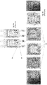
- FIGs 1a and 1b Semiconductor devices, for example MOSFET devices, are known to have a problem with excessive solder dispensed on top of die. This is shown in Figures 1a and 1b .
- a solder 10 is reaching the die edge due to a very narrow gap between the source clip and the die. This problem can be detected only using an x-ray inspection, using an electrical testing or using cross sections.
- Figure 1a shows a result of the x-ray inspection.
- Figure 2 a typical cross section of a package is shown, wherein the material layers and an excessive solder under the source clip are visible. The device will not function properly and will result to current leakages since the excessive solder is bridging 12 the drain to the source potential.
- the device needs to be completed, i.e. the whole assembly process (moulding, plating and singulation) has to be finalized, since the operator will not be able to test the MOSFET device before it is encapsulated or moulded by plastic, and singulated from the lead frame.
- the entire assembly process injection molding, plating and singulation
- many of the MOSFET devices will be already assembled and must be rejected. In case that the testing failed to filter the excessive solder due to a marginal case, the MOSFET device will not be rejected and may fail during the usage of such a MOSFET device; which obviously is not a preferred option as it may cause potential customer complaint.
- the operators can further verify any shorted device by repeating the x-ray process or by conducting a cross section which will take few days before having a result.
- all of the above steps for managing a problem of an excessive solder are not preferred since they could be expensive and/or time consuming, which is simply unacceptable in the MOSFET devices industry.
- FIG. 2a A top view, an isometric view and a side view of a known MOSFET device is shown in Figures 2a, 2b and 2c respectively. Any excessive solders, e.g. at a marked position 14 are not visible by a visual inspection.
- FIGs 3a and 3b A known solution for an excessive solder inspection is shown in Figures 3a and 3b .
- Solder inspection holes 16 are used to visually check for an excessive solder. However, this causes a narrow width 18 when the inspection holes 16 are created. Such a narrow width will cause a higher package resistance. This higher package resistance will result in more power consumption by the MOSFET device.
- the examples with the inspection holes 16 shown in Figure 3b are only applicable for wider leads. Such inspection holes are not suitable for a MOSFET device with narrow leads. For example, these inspection holes cannot be used in a dual die paddle clip bonded package. Any hole added in a narrow lead will result to an increase of a package resistance and an instability of the lead coplanarity during the stamping process.
- a semiconductor device comprises a lead frame, a die attached to the lead frame using a first solder, and a clip attached to the die using a second solder.
- the clip comprises a notch arranged for a check of the excess of the second solder. Using such a notch enables an excess solder inspection without modification of package outline, current die designs and no change in the manufacturing steps. By introducing the notch feature in the clip, it is easy for an operator to visually judge if solder is excessive or not without getting away from the manufacturing machines to perform an expensive and time-consuming x-ray inspection of the semiconductor device. Therefore, the present invention provides cost savings and prevents potential quality issues of the produced semiconductor devices.
- the notch will not contribute an increase of the package resistance since the notch does not make the width of the clip significantly narrower.
- the shape of the notch is a rectangular or a half-circle. In case that the shape of the notch is a half-circle, it is preferable that a radius of the half-circle is of the same or similar size as the thickness of the clip. In another preferred embodiment of the present invention the radius of the half-circle and the thickness of the clip are around 0.2 mm.
- the notch is made by a copper stamping or by an etching process. The copper stamping process is relatively cheap in terms of the mass production compared to the use of a chemical etching process.
- the semiconductor device is a MOSFET device, wherein the MOSFET devices comprises a source, a gate and a drain.
- the notch is positioned between the source and the drain, and/or between the gate and the drain of the MOSFET device.
- the invention also relates to a method of producing a semiconductor device, wherein the method, among other standard manufacturing steps, comprises the following steps: forming a lead frame, attaching a die to the lead frame using a first solder, and attaching a clip to the die using a second solder.
- the clip comprises a notch arranged for a check of the excess of the second solder.
- the shape of the notch can be a rectangular or a half-circle.
- a radius of such a half-circle is of the same or similar size as the thickness of the clip.
- the radius of the half-circle and the thickness of the clip are around 0.2 mm.
- the notch can be made by a copper stamping or by an etching process.
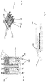
- FIGS. 4a, 4b and 4c An embodiment of the invention is shown in Figures 4a, 4b and 4c . These Figures show a top view, an isometric view and a side view respectively of a semiconductor device 100, i.e. a MOSFET device, an insulated gate bipolar transistor, a bipolar transistor, a JFET device, a thyristor, a diode, etc.
- a semiconductor device 100 i.e. a MOSFET device, an insulated gate bipolar transistor, a bipolar transistor, a JFET device, a thyristor, a diode, etc.
- the semiconductor device 100 comprises a lead frame 102, and a die 106 attached to the lead frame 102 using a first solder 104.
- a clip 120 is attached to the die 106 using a second solder 116.
- the clip 120 comprises a notch 200 arranged for a check of the excess of the second solder 116.
- the notch 200 is a side notch. Having such a notch 200 feature enables easy visual inspection of the excess of the second solder 116 in a relatively simple way, i.e. without the use of an expensive x-ray machine.
- the side notch 200 can have different shapes, for example a rectangular shape, a half circle shape (as illustrated in the example embodiment in Figures 4a, 4b and 4c ), etc.
- the notch 200 can be created by a through copper stamping, by an etching process, etc. If the notch 200 is of a half circle shape, in a preferred example embodiment a minimum size of the radius of the half circle shape is the same size as the thickness of the clip 120.
- the clip 120 can me made of copper. In a preferred embodiment of the invention the size of this radius and the thickness of the clip 120 are around 0.2 mm, or similar.
- the notch 200 is placed between the source potential and the gate potential of the semiconductor device 100 from one side and an edge of the die 106 from other side. This edge of the die 106 corresponds to the drain potential of the semiconductor device.
- a machine operator will be able to stop a possible excess of the solder and consequently to adjust a dissension of the solder immediately.
- the notch 200 is particularly designed not to reduce the width of the clip 120, so to secure that the the spreading resistance on the source terminals of the semiconductor device 100 is maintained.
- the notch 200 is provided on the clip 120 for the source of the semiconductor device and also on the clip 120 for the gate of the semiconductor device. This is particularly advantageous for the MOSFET devices that required a lower spreading resistance, and the notch 200 according to an embodiment of the invention supports such a lower spreading resistance. The notch will not contribute an increase of the package resistance since the notch 200 does not make the width of the clip 120 significantly narrower.
- Another advantage of using the notch 200 is it can be done by a copper stamping process, which is a relatively cheap in terms of the mass production compared to the use of a chemical etching process which can be 10 times more costly.
- the copper stamping process is not suitable for a narrow width of the clip, but it is suitable for the notch according to an embodiment of this invention since the width of the clip is wide enough.
- FIG. 5 A method of manufacturing a semiconductor device according to an embodiment of the invention is shown in Figure 5 .
- the method comprises the steps:
- the step 315 as shown in Figure 5 is a top view of the singulated semiconductor device. Items 317 and 319 in Figure 5 show an isometric view and a side view respectively of this singulated semiconductor device wherein inner layers are visible.
Landscapes
- Lead Frames For Integrated Circuits (AREA)
Abstract
Description
- The present invention relates to a method of forming a semiconductor device. The invention also relates to a method of manufacturing a semiconductor device.
- Semiconductor devices, for example MOSFET devices, are known to have a problem with excessive solder dispensed on top of die. This is shown in
Figures 1a and 1b . Asolder 10 is reaching the die edge due to a very narrow gap between the source clip and the die. This problem can be detected only using an x-ray inspection, using an electrical testing or using cross sections.Figure 1a shows a result of the x-ray inspection. InFigure 2 a typical cross section of a package is shown, wherein the material layers and an excessive solder under the source clip are visible. The device will not function properly and will result to current leakages since the excessive solder is bridging 12 the drain to the source potential. - This known problem where an uncontrolled solder is dispensed on the source solderable top contact, which results to an excessive amount of solder, which causes the bridging between the drain and the source/the gate of a MOSFET device.
- There are some known methods of solving the problem described above. Some of these methods require a major change of a die design, which is very expensive and inefficient. Other possibility is to provide an additional excess solder detection equipment, which also will be an expensive and inefficient option. Furthermore, a change of a MOSFET device package outline can be done, but this will result in a modification of a mould tool and trim forming singulation tool (TFS). Similarly to the previous options, this one will be also very expensive and inefficient to implement. In general, any changes that will impact a die size, an electrical performance and a package outline will be very difficult, and therefore expensive and inefficient, to implement.
- Normally the production operators will follow the succeeding steps for an additional excess solder detection when manufacturing a MOSFET device. Firstly, an operator will pull out few production-assembled samples to check for an excessive solder by bringing these to x-ray room, which can be located in a different area. If there are darker images or shadow observed under the clips, this is an indication that an excessive amount of solder has been dispensed. The operators will then go back to the machine and adjust the solder dispense settings. They will repeat the process until they do not see traces of excessive solder under the clips anymore. Secondly, if an operator failed or missed to check the samples by x-ray, the next possibility to check for an excessive solder problem is by conducting electrical testing. However, before this final test can take place, the device needs to be completed, i.e. the whole assembly process (moulding, plating and singulation) has to be finalized, since the operator will not be able to test the MOSFET device before it is encapsulated or moulded by plastic, and singulated from the lead frame. Thus, before the excessive solder was found out by the final testing, many of the MOSFET devices will be already assembled and must be rejected. In case that the testing failed to filter the excessive solder due to a marginal case, the MOSFET device will not be rejected and may fail during the usage of such a MOSFET device; which obviously is not a preferred option as it may cause potential customer complaint. Thirdly, the operators can further verify any shorted device by repeating the x-ray process or by conducting a cross section which will take few days before having a result. To conclude, all of the above steps for managing a problem of an excessive solder are not preferred since they could be expensive and/or time consuming, which is simply unacceptable in the MOSFET devices industry.
- A top view, an isometric view and a side view of a known MOSFET device is shown in
Figures 2a, 2b and 2c respectively. Any excessive solders, e.g. at a markedposition 14 are not visible by a visual inspection. - A known solution for an excessive solder inspection is shown in
Figures 3a and 3b .Solder inspection holes 16 are used to visually check for an excessive solder. However, this causes anarrow width 18 when theinspection holes 16 are created. Such a narrow width will cause a higher package resistance. This higher package resistance will result in more power consumption by the MOSFET device. The examples with theinspection holes 16 shown inFigure 3b are only applicable for wider leads. Such inspection holes are not suitable for a MOSFET device with narrow leads. For example, these inspection holes cannot be used in a dual die paddle clip bonded package. Any hole added in a narrow lead will result to an increase of a package resistance and an instability of the lead coplanarity during the stamping process. - To conclude, none of the solutions for an excessive solder inspection as described above is not suitable for MOSFET and other semiconductor devices where narrow leads are required.
- Various example embodiments are directed to the disadvantage as described above and/or others which may become apparent from the following disclosure.
- According to an embodiment of this invention a semiconductor device comprises a lead frame, a die attached to the lead frame using a first solder, and a clip attached to the die using a second solder. The clip comprises a notch arranged for a check of the excess of the second solder.
Using such a notch enables an excess solder inspection without modification of package outline, current die designs and no change in the manufacturing steps.
By introducing the notch feature in the clip, it is easy for an operator to visually judge if solder is excessive or not without getting away from the manufacturing machines to perform an expensive and time-consuming x-ray inspection of the semiconductor device. Therefore, the present invention provides cost savings and prevents potential quality issues of the produced semiconductor devices.
Furthermore, the notch will not contribute an increase of the package resistance since the notch does not make the width of the clip significantly narrower.
According to an embodiment of the invention, the shape of the notch is a rectangular or a half-circle. In case that the shape of the notch is a half-circle, it is preferable that a radius of the half-circle is of the same or similar size as the thickness of the clip. In another preferred embodiment of the present invention the radius of the half-circle and the thickness of the clip are around 0.2 mm.
In an embodiment of the present invention the notch is made by a copper stamping or by an etching process. The copper stamping process is relatively cheap in terms of the mass production compared to the use of a chemical etching process. - In a preferred embodiment of the present invention the semiconductor device is a MOSFET device, wherein the MOSFET devices comprises a source, a gate and a drain. The notch is positioned between the source and the drain, and/or between the gate and the drain of the MOSFET device.
- The invention also relates to a method of producing a semiconductor device, wherein the method, among other standard manufacturing steps, comprises the following steps: forming a lead frame, attaching a die to the lead frame using a first solder, and attaching a clip to the die using a second solder. The clip comprises a notch arranged for a check of the excess of the second solder. Again, the shape of the notch can be a rectangular or a half-circle. In case that the shape of the notch is a half-circle, in a preferred embodiment of the present invention a radius of such a half-circle is of the same or similar size as the thickness of the clip. Preferably, the radius of the half-circle and the thickness of the clip are around 0.2 mm. The notch can be made by a copper stamping or by an etching process.
- So that the manner in which the features of the present disclosure can be understood in detail, a more particular description is made with reference to embodiments, some of which are illustrated in the appended figures. It is to be noted, however, that the appended figures illustrate only typical embodiments and are therefore not to be considered limiting of its scope. The figures are for facilitating an understanding of the disclosure and thus are not necessarily drawn to scale. Advantages of the subject matter claimed will become apparent to those skilled in the art upon reading this description in conjunction with the accompanying figures, in which like reference numerals have been used to designate like elements, and in which:
-
Figures 1a and 1b show a known MOSFET device wherein an excessive solder is dispensed on the top of the die; -
Figures 2a, 2b and 2c show a top view, an isometric view and a side view respectively of a known MOSFET device; -
Figures 3a and 3b show known MOSFET devices with solder inspection holes; -
Figures 4a, 4b and 4c show a top view, an isometric view and a side view respectively of a semiconductor device according to an embodiment of the invention; -
Figure 5 shows a method of manufacturing of a semiconductor device according to an embodiment of this invention. - An embodiment of the invention is shown in
Figures 4a, 4b and 4c . These Figures show a top view, an isometric view and a side view respectively of asemiconductor device 100, i.e. a MOSFET device, an insulated gate bipolar transistor, a bipolar transistor, a JFET device, a thyristor, a diode, etc. - The
semiconductor device 100 comprises alead frame 102, and adie 106 attached to thelead frame 102 using afirst solder 104. Aclip 120 is attached to the die 106 using asecond solder 116. Theclip 120 comprises anotch 200 arranged for a check of the excess of thesecond solder 116. In the example shown inFigures 4a, 4b and 4c , thenotch 200 is a side notch. Having such anotch 200 feature enables easy visual inspection of the excess of thesecond solder 116 in a relatively simple way, i.e. without the use of an expensive x-ray machine. - The
side notch 200 can have different shapes, for example a rectangular shape, a half circle shape (as illustrated in the example embodiment inFigures 4a, 4b and 4c ), etc. Thenotch 200 can be created by a through copper stamping, by an etching process, etc. If thenotch 200 is of a half circle shape, in a preferred example embodiment a minimum size of the radius of the half circle shape is the same size as the thickness of theclip 120. Theclip 120 can me made of copper. In a preferred embodiment of the invention the size of this radius and the thickness of theclip 120 are around 0.2 mm, or similar. - It is recommended to provide such a
notch 200 in the places where the excess of the solder should be checked. In an example embodiment of this invention thenotch 200 is placed between the source potential and the gate potential of thesemiconductor device 100 from one side and an edge of the die 106 from other side. This edge of thedie 106 corresponds to the drain potential of the semiconductor device. Within the production of thesemiconductor device 100, due to the present of thenotch 200, a machine operator will be able to stop a possible excess of the solder and consequently to adjust a dissension of the solder immediately. - The
notch 200 is particularly designed not to reduce the width of theclip 120, so to secure that the the spreading resistance on the source terminals of thesemiconductor device 100 is maintained. - By introducing the
notch 200 in theclip 120, the problems of the prior art described above are solved. An operator can visually judge if the solder is excessive. There is no need to use other expensive and inefficient methods mentioned above, such as a x-ray inspection of the semiconductor device. Thus, the implementation of this invention clearly saves costs and prevents possible quality issues that can be caused by the excess of the solder. - As it is shown in the example embodiment in
Figures 4a and 4b , thenotch 200 is provided on theclip 120 for the source of the semiconductor device and also on theclip 120 for the gate of the semiconductor device. This is particularly advantageous for the MOSFET devices that required a lower spreading resistance, and thenotch 200 according to an embodiment of the invention supports such a lower spreading resistance. The notch will not contribute an increase of the package resistance since thenotch 200 does not make the width of theclip 120 significantly narrower. - Another advantage of using the
notch 200 is it can be done by a copper stamping process, which is a relatively cheap in terms of the mass production compared to the use of a chemical etching process which can be 10 times more costly. The copper stamping process is not suitable for a narrow width of the clip, but it is suitable for the notch according to an embodiment of this invention since the width of the clip is wide enough. - A method of manufacturing a semiconductor device according to an embodiment of the invention is shown in
Figure 5 . - The method comprises the steps:
- step 301: providing a
lead frame 102 which can be stamped or etched bottom - step 303: print, write or dispense a
first solder 104 on thelead frame 102 - step 305: forming a die 106 attached to the
lead frame 102 using afirst solder 104 - step 307: print, write or dispense a
second solder 116 on thedie 106 - step 309: forming
clips 120 comprising anotch 200 and attaching theclips 120 on top of the silicon die 106; theclips 120 contain source and gate terminals; adambar 124 is connecting these terminals; so assembled parts will then go towards a reflow process to cure the solidify or to cure the solder applied - step 311: perform a moulding of the cured and assembled device from the previous step, so to encapsulate the silicon with an
encapsulant 122; an encapsulation is required to protect the silicon dies from any oxidation and contamination; the product will further undergo tin (Sn) plating process after moulding so to plate external leads in order to protect the copper from oxidation - step 313: perform trim/form/singulation (TFS) process wherein some parts of the lead frames and clips will be removed to make the final semiconductor device
- step 315: perform cut of the
dambar 124, wherein the singulated semiconductor device is created - The
step 315 as shown inFigure 5 is a top view of the singulated semiconductor device.Items 317 and 319 inFigure 5 show an isometric view and a side view respectively of this singulated semiconductor device wherein inner layers are visible. - Particular and preferred aspects of the invention are set out in the accompanying independent claims. Combinations of features from the dependent and/or independent claims may be combined as appropriate and not merely as set out in the claims.
- The scope of the present disclosure includes any novel feature or combination of features disclosed therein either explicitly or implicitly or any generalisation thereof irrespective of whether or not it relates to the claimed invention or mitigate against any or all of the problems addressed by the present invention. The applicant hereby gives notice that new claims may be formulated to such features during prosecution of this application or of any such further application derived therefrom. In particular, with reference to the appended claims, features from dependent claims may be combined with those of the independent claims and features from respective independent claims may be combined in any appropriate manner and not merely in specific combinations enumerated in the claims.
- Features which are described in the context of separate embodiments may also be provided in combination in a single embodiment. Conversely, various features which are, for brevity, described in the context of a single embodiment, may also be provided separately or in any suitable sub combination.
- Term "comprising" does not exclude other elements or steps, the term "a" or "an" does not exclude a plurality. Reference signs in the claims shall not be construed as limiting the scope of the claims.
Claims (11)
- A semiconductor device comprising:- a lead frame,- a die attached to the lead frame using a first solder,- a clip attached to the die using a second solder,
wherein the clip comprises a notch arranged for a check of the excess of the second solder. - A semiconductor device as claimed in claim 1, wherein the shape of the notch is a rectangular or a half-circle.
- A semiconductor device as claimed in any of the previous claims, wherein the notch is made by a copper stamping or by an etching process.
- A semiconductor device as claimed in claim 2, wherein the shape of the notch is a half-circle and wherein a radius of the half-circle is of the same or similar size as the thickness of the clip.
- A semiconductor device as claimed in claim 4, where the radius of the half-circle and the thickness of the clip are around 0.2 mm.
- A semiconductor device as claimed in any of the previous claims, wherein the semiconductor device is a transistor (a MOSFET device), the transistor (the MOSFET device) comprising a source, a gate and a drain, wherein the notch is positioned between the source and the drain, and/or between the gate and the drain.
- A method of producing a semiconductor device, the method comprising the steps:• forming a lead frame,• attaching a die to the lead frame using a first solder,• attaching a clip to the die using a second solder,
wherein the clip comprises a notch arranged for a check of the excess of the second solder. - A method of producing a semiconductor device as claimed in claim 7, wherein the shape of the notch is a rectangular or a half-circle.
- A method of producing a semiconductor device as claimed in claims 7 or 8, wherein the notch is made by a copper stamping or by an etching process.
- A method of producing a semiconductor device as claimed in claim 8, wherein the shape of the notch is a half-circle and wherein a radius of the half-circle is of the same or similar size as the thickness of the clip.
- A method of producing a semiconductor device as claimed in claim 10, where the radius of the half-circle and the thickness of the clip are around 0.2 mm.
Priority Applications (3)
| Application Number | Priority Date | Filing Date | Title |
|---|---|---|---|
| EP20172575.1A EP3905324A1 (en) | 2020-05-01 | 2020-05-01 | A semiconductor device and a method of manufacture |
| CN202110473369.4A CN113594125B (en) | 2020-05-01 | 2021-04-29 | Semiconductor device and method for manufacturing the same |
| US17/245,519 US12347751B2 (en) | 2020-05-01 | 2021-04-30 | Semiconductor device and a method of manufacture |
Applications Claiming Priority (1)
| Application Number | Priority Date | Filing Date | Title |
|---|---|---|---|
| EP20172575.1A EP3905324A1 (en) | 2020-05-01 | 2020-05-01 | A semiconductor device and a method of manufacture |
Publications (1)
| Publication Number | Publication Date |
|---|---|
| EP3905324A1 true EP3905324A1 (en) | 2021-11-03 |
Family
ID=70483043
Family Applications (1)
| Application Number | Title | Priority Date | Filing Date |
|---|---|---|---|
| EP20172575.1A Pending EP3905324A1 (en) | 2020-05-01 | 2020-05-01 | A semiconductor device and a method of manufacture |
Country Status (3)
| Country | Link |
|---|---|
| US (1) | US12347751B2 (en) |
| EP (1) | EP3905324A1 (en) |
| CN (1) | CN113594125B (en) |
Families Citing this family (2)
| Publication number | Priority date | Publication date | Assignee | Title |
|---|---|---|---|---|
| CN116072647B (en) * | 2023-03-28 | 2023-07-18 | 深圳市深鸿盛电子有限公司 | A kind of MOS chip package structure and package method thereof |
| US12581990B2 (en) * | 2023-08-14 | 2026-03-17 | Littlefuse, Inc. | Metal tab for power semiconductor module |
Citations (4)
| Publication number | Priority date | Publication date | Assignee | Title |
|---|---|---|---|---|
| JP2009038126A (en) * | 2007-07-31 | 2009-02-19 | Sanyo Electric Co Ltd | Semiconductor apparatus and method of manufacturing the same |
| EP2930747A1 (en) * | 2014-04-07 | 2015-10-14 | Nxp B.V. | Lead for connection to a semiconductor device |
| US20170069563A1 (en) * | 2015-09-04 | 2017-03-09 | Kabushiki Kaisha Toshiba | Semiconductor package and method of manufacturing semiconductor package |
| US20180350726A1 (en) * | 2017-06-06 | 2018-12-06 | Amkor Technology, Inc. | Semiconductor package having inspection structure and related methods |
Family Cites Families (5)
| Publication number | Priority date | Publication date | Assignee | Title |
|---|---|---|---|---|
| US6946740B2 (en) * | 2002-07-15 | 2005-09-20 | International Rectifier Corporation | High power MCM package |
| US9589929B2 (en) * | 2013-03-14 | 2017-03-07 | Vishay-Siliconix | Method for fabricating stack die package |
| US8884420B1 (en) * | 2013-07-12 | 2014-11-11 | Infineon Technologies Austria Ag | Multichip device |
| US9870985B1 (en) * | 2016-07-11 | 2018-01-16 | Amkor Technology, Inc. | Semiconductor package with clip alignment notch |
| US10553524B2 (en) * | 2017-10-30 | 2020-02-04 | Microchip Technology Incorporated | Integrated circuit (IC) die attached between an offset lead frame die-attach pad and a discrete die-attach pad |
-
2020
- 2020-05-01 EP EP20172575.1A patent/EP3905324A1/en active Pending
-
2021
- 2021-04-29 CN CN202110473369.4A patent/CN113594125B/en active Active
- 2021-04-30 US US17/245,519 patent/US12347751B2/en active Active
Patent Citations (4)
| Publication number | Priority date | Publication date | Assignee | Title |
|---|---|---|---|---|
| JP2009038126A (en) * | 2007-07-31 | 2009-02-19 | Sanyo Electric Co Ltd | Semiconductor apparatus and method of manufacturing the same |
| EP2930747A1 (en) * | 2014-04-07 | 2015-10-14 | Nxp B.V. | Lead for connection to a semiconductor device |
| US20170069563A1 (en) * | 2015-09-04 | 2017-03-09 | Kabushiki Kaisha Toshiba | Semiconductor package and method of manufacturing semiconductor package |
| US20180350726A1 (en) * | 2017-06-06 | 2018-12-06 | Amkor Technology, Inc. | Semiconductor package having inspection structure and related methods |
Also Published As
| Publication number | Publication date |
|---|---|
| CN113594125A (en) | 2021-11-02 |
| US12347751B2 (en) | 2025-07-01 |
| US20210343627A1 (en) | 2021-11-04 |
| CN113594125B (en) | 2023-03-03 |
Similar Documents
| Publication | Publication Date | Title |
|---|---|---|
| KR102325824B1 (en) | Method of manufacturing semiconductor device | |
| US3413713A (en) | Plastic encapsulated transistor and method of making same | |
| US9905482B2 (en) | Method of manufacturing a semiconductor device and inspecting an electrical characteristic thereof using test socket terminals | |
| US4012766A (en) | Semiconductor package and method of manufacture thereof | |
| US12347751B2 (en) | Semiconductor device and a method of manufacture | |
| US7554179B2 (en) | Multi-leadframe semiconductor package and method of manufacture | |
| US3444441A (en) | Semiconductor devices including lead and plastic housing structure suitable for automated process construction | |
| US11348806B2 (en) | Making a flat no-lead package with exposed electroplated side lead surfaces | |
| CN104854695A (en) | Lead carrier with printed formed terminal pads | |
| US9620388B2 (en) | Integrated circuit package fabrication with die attach paddle having middle channels | |
| KR20150105923A (en) | Semiconductor device and method of manufacturing the same | |
| EP2361000A1 (en) | Leadless chip package mounting method and carrier | |
| CN105742269A (en) | Method of Manufacturing Semiconductor Device | |
| US20190348335A1 (en) | Method of manufacturing a semiconductor device | |
| CN104659009A (en) | Method Of Minimizing Mold Flash During Dambar Cut | |
| CN107946259A (en) | A kind of QFN encapsulating structures and its manufacture method | |
| US5347709A (en) | Method of making lead frame | |
| JP2018195720A (en) | Manufacturing method of semiconductor device | |
| US20250391744A1 (en) | Semiconductor device including a coined diepad | |
| CN110783303B (en) | Lead frame for die | |
| DE102024129374A1 (en) | Semiconductor device package with an internal magnetic shield for a Hall sensor | |
| CN119230505A (en) | Semiconductor device and method for manufacturing the same | |
| KR100257405B1 (en) | Micro BIG Package Manufacturing Method | |
| JPH04340742A (en) | Discrimination method of imperfect semiconductor device | |
| JP2018117031A (en) | Manufacturing method of lead frame |
Legal Events
| Date | Code | Title | Description |
|---|---|---|---|
| PUAI | Public reference made under article 153(3) epc to a published international application that has entered the european phase |
Free format text: ORIGINAL CODE: 0009012 |
|
| STAA | Information on the status of an ep patent application or granted ep patent |
Free format text: STATUS: THE APPLICATION HAS BEEN PUBLISHED |
|
| AK | Designated contracting states |
Kind code of ref document: A1 Designated state(s): AL AT BE BG CH CY CZ DE DK EE ES FI FR GB GR HR HU IE IS IT LI LT LU LV MC MK MT NL NO PL PT RO RS SE SI SK SM TR |
|
| B565 | Issuance of search results under rule 164(2) epc |
Effective date: 20200713 |
|
| STAA | Information on the status of an ep patent application or granted ep patent |
Free format text: STATUS: REQUEST FOR EXAMINATION WAS MADE |
|
| 17P | Request for examination filed |
Effective date: 20220429 |
|
| RBV | Designated contracting states (corrected) |
Designated state(s): AL AT BE BG CH CY CZ DE DK EE ES FI FR GB GR HR HU IE IS IT LI LT LU LV MC MK MT NL NO PL PT RO RS SE SI SK SM TR |