EP3905252A1 - Read-write circuit of one-time programmable memory - Google Patents
Read-write circuit of one-time programmable memory Download PDFInfo
- Publication number
- EP3905252A1 EP3905252A1 EP20894324.1A EP20894324A EP3905252A1 EP 3905252 A1 EP3905252 A1 EP 3905252A1 EP 20894324 A EP20894324 A EP 20894324A EP 3905252 A1 EP3905252 A1 EP 3905252A1
- Authority
- EP
- European Patent Office
- Prior art keywords
- node
- switching element
- antifuse
- read
- coupled
- Prior art date
- Legal status (The legal status is an assumption and is not a legal conclusion. Google has not performed a legal analysis and makes no representation as to the accuracy of the status listed.)
- Granted
Links
Images



Classifications
-
- G—PHYSICS
- G11—INFORMATION STORAGE
- G11C—STATIC STORES
- G11C17/00—Read-only memories programmable only once; Semi-permanent stores, e.g. manually-replaceable information cards
- G11C17/14—Read-only memories programmable only once; Semi-permanent stores, e.g. manually-replaceable information cards in which contents are determined by selectively establishing, breaking or modifying connecting links by permanently altering the state of coupling elements, e.g. PROM
- G11C17/16—Read-only memories programmable only once; Semi-permanent stores, e.g. manually-replaceable information cards in which contents are determined by selectively establishing, breaking or modifying connecting links by permanently altering the state of coupling elements, e.g. PROM using electrically-fusible links
- G11C17/165—Memory cells which are electrically programmed to cause a change in resistance, e.g. to permit multiple resistance steps to be programmed rather than conduct to or from non-conduct change of fuses and antifuses
-
- G—PHYSICS
- G11—INFORMATION STORAGE
- G11C—STATIC STORES
- G11C17/00—Read-only memories programmable only once; Semi-permanent stores, e.g. manually-replaceable information cards
- G11C17/14—Read-only memories programmable only once; Semi-permanent stores, e.g. manually-replaceable information cards in which contents are determined by selectively establishing, breaking or modifying connecting links by permanently altering the state of coupling elements, e.g. PROM
- G11C17/16—Read-only memories programmable only once; Semi-permanent stores, e.g. manually-replaceable information cards in which contents are determined by selectively establishing, breaking or modifying connecting links by permanently altering the state of coupling elements, e.g. PROM using electrically-fusible links
-
- G—PHYSICS
- G11—INFORMATION STORAGE
- G11C—STATIC STORES
- G11C17/00—Read-only memories programmable only once; Semi-permanent stores, e.g. manually-replaceable information cards
- G11C17/04—Read-only memories programmable only once; Semi-permanent stores, e.g. manually-replaceable information cards using capacitive elements
-
- G—PHYSICS
- G11—INFORMATION STORAGE
- G11C—STATIC STORES
- G11C17/00—Read-only memories programmable only once; Semi-permanent stores, e.g. manually-replaceable information cards
- G11C17/14—Read-only memories programmable only once; Semi-permanent stores, e.g. manually-replaceable information cards in which contents are determined by selectively establishing, breaking or modifying connecting links by permanently altering the state of coupling elements, e.g. PROM
- G11C17/18—Auxiliary circuits, e.g. for writing into memory
-
- G—PHYSICS
- G11—INFORMATION STORAGE
- G11C—STATIC STORES
- G11C7/00—Arrangements for writing information into, or reading information out from, a digital store
- G11C7/10—Input/output [I/O] data interface arrangements, e.g. I/O data control circuits, I/O data buffers
- G11C7/1051—Data output circuits, e.g. read-out amplifiers, data output buffers, data output registers, data output level conversion circuits
- G11C7/1069—I/O lines read out arrangements
-
- G—PHYSICS
- G11—INFORMATION STORAGE
- G11C—STATIC STORES
- G11C7/00—Arrangements for writing information into, or reading information out from, a digital store
- G11C7/10—Input/output [I/O] data interface arrangements, e.g. I/O data control circuits, I/O data buffers
- G11C7/1078—Data input circuits, e.g. write amplifiers, data input buffers, data input registers, data input level conversion circuits
- G11C7/1096—Write circuits, e.g. I/O line write drivers
-
- G—PHYSICS
- G11—INFORMATION STORAGE
- G11C—STATIC STORES
- G11C7/00—Arrangements for writing information into, or reading information out from, a digital store
- G11C7/22—Read-write [R-W] timing or clocking circuits; Read-write [R-W] control signal generators or management
Definitions
- the present disclosure relates to the technical field of integrated circuits, and in particular to a read-write circuit of a one-time programmable memory.
- One Time Programmable (OTP) memory can store data in multiple OTP units which are either in an unprogrammed state or in a programmed state.
- An OTP unit usually includes a fuse element or an antifuse element. After the fuse element or the antifuse element is programmed, it will be in an unrecoverable state. This unrecoverable state will not be affected by power failures, so that data can be stored stably.
- an OTP unit is often used to control the opening or closing of a redundancy memory unit.
- DRAM Dynamic Random Access Memory
- the corresponding OTP unit will be programmed (the output state of the OTP unit changes from "0" to "1"), and the DRAM control circuit will turn off the reading and writing of the memory unit in the memory unit area, and will open the reading and writing of a memory unit in a redundant area, which then will replace the memory unit in the defective memory unit area with the corresponding memory unit in the redundant area, thereby repairing the DRAM defect.
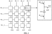
- FIG. 1 is a schematic diagram of a read-write circuit of an OTP unit in the related art. It can be seen from FIG. 1 that each memory unit is connected with a corresponding antifuse element and a detection element.
- This connection method in a large-scale integrated circuit will cause problems such as circuit area being too large and wiring being too complex. Due to the numerous components and complicated wiring, circuit reliability will be reduced as a result.
- the present disclosure provides a read-write circuit of a one-time programmable memory, which is used to overcome some of the problems such as large areas and complexity of the read-write circuits and low reliability caused by limitations and faults of the existing techniques.
- One aspect of the present disclosure provides a read-write circuit of a one-time programmable memory, including:
- the first switching element in a writing state, is turned on and the second switching element is turned off; and wherein in a reading state, the first control signal and the second control signal are pulse signals having a same phase.
- a ratio of the voltage of the second node to the voltage of the third node is greater than a first preset value, or the ratio of the voltage of the second node to the voltage of the third node is less than a second preset value.
- the first switching element and the second switching element are turned on at a same time.
- the first voltage source in the writing state, is at a first voltage level, wherein in the reading state, the first voltage source is at a second voltage level, and wherein the first voltage level is greater than the second voltage level.
- the first switching element, the second switching element, and the reference switching element are all negative channel Metal Oxide Semiconductor (NMOS) switching transistors.
- NMOS Metal Oxide Semiconductor
- a resistance value of the reference resistor is smaller than a blocking-resistance value of the antifuse element and greater than an on-resistance value of the antifuse element.
- a resistance value of the reference resistor is less than or equal to one tenth of a blocking-resistance value of the antifuse element, and greater than or equal to ten times of an on-resistance value of the antifuse element.
- the reference resistor is a variable resistor.
- capacitance values of the first capacitor and the second capacitor are equal.
- the embodiments of the present disclosure realize the following: n ⁇ n antifuse units connected between the first node and the second node, a control signal controlling the opening and closing states of an antifuse unit, and the parallel connection of the first switching element and the first capacitor at the second node, the second node connected to the input of the comparator, and one reference array capable to compare the voltages at the second node, all of which achieved detection of the fuse states with a smaller number of components and a smaller circuit area, resulting improved reliability of the circuit.
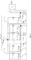
- FIG. 2 is a schematic diagram of the structure in an exemplary embodiment of the present disclosure.
- the read-write circuit 100 may include antifuse array 21, reference array 22, and comparison circuit 23.
- the antifuse array 21 includes:
- the reference array 22 includes:
- the comparison circuit 23 has the first input terminal coupled to the second node N2 and the second input terminal coupled to the third node N3, for determining whether a corresponding antifuse element of the antifuse array has a programming operation based on the voltage comparison result of the second node N2 and the third node N3.
- the antifuse element may compose a MOS transistor, equivalent to a capacitor, which is in an off state before being programmed, and is in an on state after being programmed.
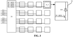
- FIG. 3 is a schematic diagram of the signal connection of the antifuse unit in the circuit shown in FIG. 2 .
- each antifuse unit 32 is connected to only one control signal line, and the control signal line is connected to the output terminal of the logic circuit 31 for outputting the AND signals WL_x & BL_y from different word line signals WL_x and bit line signals BL_y.
- the input terminal of the logic circuit 31 is connected to all word lines and bit lines. When the numbers of word lines and bit lines are large, the logic circuit 31 can convert m+n word line/bit line signals into m ⁇ n control signals. Compared with the complicated circuit connections in FIG. 1 (each fuse/antifuse unit needs to connect to three signal lines), the circuit connections of the antifuse units disclosed in the present embodiment are simpler and takes up less area.
- FIG. 4 is a timing diagram of control signals of the read-write circuit according to an embodiment of the present disclosure.
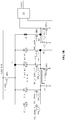
- FIG. 5A to FIG. 5C are schematic diagrams of the circuit states corresponding to the control timing shown in FIG. 4 .
- the first switching element MN1, the second switching element MN2, the reference switching element MN3, and the switching elements in each antifuse unit are all NMOS switching transistors. At this time, each switching element is turned on at a high voltage level and turned off at a low voltage level. In other embodiments, each switching element may also be a positive channel Metal Oxide Semiconductor (PMOS) switching transistor. In this case, the control signal may be adaptively adjusted according to the switching characteristics of the PMOS switching transistor, and the present disclosure is not limited to this example.
- PMOS Metal Oxide Semiconductor
- the first voltage source VDD_W/R in the writing state (when the antifuse unit is programmed), the first voltage source VDD_W/R is at the first voltage level, and in the read state (when the state of the antifuse unit is detected), the first voltage source VDD_W/R is at the second voltage level.
- the first voltage level is a high voltage (for example, 5 ⁇ 6V)
- the second voltage level is a low voltage (for example, 1.0 ⁇ 1.2V).
- the first control signal V_CTRL1 is at a high voltage level
- the first switching element is turned on
- the second control signal V_CTRL2 is at a low voltage level
- the second switching element is turned off.
- the switching transistor of a certain antifuse unit is turned on, both ends of a certain antifuse element connected to the first voltage source and the second voltage source realize fused open, and the state changes irreversibly.
- the first control signal V_CTRL1 and the second control signal V CTRL2 are pulse signals with the same phase, and each pulse corresponds to one read signal output (one word line is in the enable state and one bit line is in the enable state), therefore, in one cycle of the pulse signal, the first switching element and the second switching element undergo a simultaneous turn-on and simultaneous turn-off.
- word line x is in the enabled state
- bit line y is in the enabled state
- the control signal of the reference device MN3 is in the enabled state
- the reference switching element MN3 is turned on. Therefore, in the read state, as long as any antifuse unit in the antifuse array is in the enabled state, the reference switching element MN3 is turned on. Similarly, if all the antifuse units in the antifuse array are not enabled, then the reference switching element MN3 is turned off.
- the voltage of the second node is zero, and the first capacitor C1 discharges through the first switching element MN1; the voltage of the third node N3 is zero, and the second capacitor C2 discharges through the second switching element MN2. Therefore, in this interval, the voltages on the first capacitor C1 and the second capacitor C2 are both zero, in preparation for charging.
- the first voltage source charges the second capacitor C2 through the mirror current source MP1, the reference resistor R1 and the reference switching element MN3, and the voltage of the third node N3 depends on the charging speed of the second capacitor C2.
- the first voltage source charges the first capacitor C1 through the mirror current source MP1, the blocking resistor of the antifuse element C_x_y, and the switching element MN_x_y, and the voltage of the second node N2 depends on the charging speed of the first capacitor C1.
- the first voltage source charges the first capacitor C1 through the mirror current source MP1, the on-resistance of the antifuse element C_x_y and the switching element MN_x_y, and the voltage of the second node N2 depends on the charging speed of the first capacitor C1.
- the comparison circuit 23 determines whether the currently read antifuse unit is programmed by comparing the voltages of the second node N2 and the third node N3. For example, in the T2 stage in FIG. 4 , since Vn2 is significantly greater than Vn3 for a period of time, it can be determined that the current read antifuse unit is in the enabled state; in the T4 stage in FIG. 4 , Vn2 is significantly smaller than Vn3 in a period of time, it can be determined that the current read antifuse unit is in the disabled state.
- the charging speeds of the first capacitor and the second capacitor are controlled to maintain the voltage difference between the first capacitor and the second capacitor for a certain period of time, thereby achieving voltage comparison.
- the method of controlling the charging speed of the first capacitor and the second capacitor includes reducing the overall charging speeds and controlling the charging speed difference by the differences of resistance values.
- the capacitance values of the first capacitor and the second capacitor may be set equal.
- the method of reducing the overall charging speeds is, for example, by controlling the gate voltage of the mirror current source MP1.
- the control terminal of the mirror current source MP1 is connected to the control signal V_MIR, and the control signal V MIR is provided by the voltage source/current source module.
- V MIR the control signal
- the mirror current magnitude can be set when the mirror current source MP1 is turned on.
- its current can be determined according to the capacitance values (based on charging time) of the first capacitor C1 and the second capacitor C2. For example, when the capacitances of the first capacitor and the second capacitor are equal, and the capacitances of the first capacitor and the second capacitor are both in the range of 1 ⁇ 1000fF, the mirror current can be set to 1 ⁇ 100nA.
- the method of controlling the difference in charging speed by the difference in resistance values may be, for example, setting the resistance value of the reference resistor R1 according to the resistances of the antifuse element before and after programming, that is, the blocking-resistance and the on-resistance.
- the blocking-resistance value of the antifuse element is R_NP when it is not broken down
- the on-resistance value is R_P after it is broken down
- the resistance of resistor R1 should be greater than R_P but less than R_NP, that is, the resistance of the reference resistor is set to be greater than the on-resistance value of the antifuse element but smaller than the blocking-resistance value of the antifuse element.
- R_P is two orders of magnitude or less smaller than R_NP. Therefore, in the present disclosure, R1 is set to be one order of magnitude larger than R_P, and R_NP is set to be one order of magnitude larger than R1, that is, the resistance of the reference resistor can be set less than or equal to one-tenth of the blocking-resistance of the antifuse element, and greater than or equal to ten times the on-resistance of the antifuse element.
- the resistance of the reference resistor R1 can be further determined by the preset charging time ratio of the capacitors C1 and C2 according to the design requirements. Finally, when the capacitances of the first capacitor C1 and the second capacitor C2 is in the range of 1 ⁇ 1000fF, the resistance value of the reference resistor R1 can be set in the range of 1K ⁇ 100K ⁇ .
- the reference resistor R1 may be a fixed resistor or an adjustable resistor. Since the resistance value of a fixed resistor usually has an error, setting the reference resistor R1 as an adjustable resistor helps to provide more accurate control over capacitor charging time.
- the first voltage source VDD_W/R charges the first capacitor C1 through the mirror current source MP1, the blocking-resistance of the antifuse element C_x_y and the switching element MN_x_y, and charges the second capacitor C2 through the mirror current source MP1, the reference resistor R1, and the reference switching element MN3.
- the voltage Vn3 of the third node N3 is 10 times the voltage Vn2 of the second node N2 within a period of time.
- the first voltage source VDD_W/R charges the first capacitor C1 through the mirror current source MP1, the on-resistance of the antifuse element C_x_y and the switching element MN_x_y, and charges the second capacitor C2 through the mirror current source MP1, the reference resistor R1, and the reference switching element MN3.
- R001 blocking-resistance
- R002 on-resistance
- the voltage Vn3 of the third node N3 is one-tenth of the voltage Vn2 of the second node N2 within a period of time.
- the comparator 23 does not need to be highly sensitive to determine the status of the antifuse unit, thereby can greatly reduce the components' cost.
- the present disclosure is able to not only simplify circuit connections and reduce the number of components, thereby improving circuit reliability, but also capable of reducing the parameter requirements for components, further saving manufacturing cost.
- the embodiments of the present disclosure realize the following: n ⁇ n antifuse units connected between the first node and the second node, a control signal controlling the opening and closing states of an antifuse unit, and the parallel connection of the first switching element and the first capacitor at the second node, the second node connected to the input of the comparator, and one reference array capable to compare the voltages at the second node, all of which achieved detection of the fuse states with a smaller number of components and a smaller circuit area, resulting improved reliability of the circuit.
Landscapes
- Read Only Memory (AREA)
- Design And Manufacture Of Integrated Circuits (AREA)
Abstract
Description
- The present disclosure relates to the technical field of integrated circuits, and in particular to a read-write circuit of a one-time programmable memory.
- One Time Programmable (OTP) memory can store data in multiple OTP units which are either in an unprogrammed state or in a programmed state. An OTP unit usually includes a fuse element or an antifuse element. After the fuse element or the antifuse element is programmed, it will be in an unrecoverable state. This unrecoverable state will not be affected by power failures, so that data can be stored stably.
- In Dynamic Random Access Memory (DRAM), an OTP unit is often used to control the opening or closing of a redundancy memory unit. For example, when a memory unit in a memory unit area corresponding to a word line is defective, the corresponding OTP unit will be programmed (the output state of the OTP unit changes from "0" to "1"), and the DRAM control circuit will turn off the reading and writing of the memory unit in the memory unit area, and will open the reading and writing of a memory unit in a redundant area, which then will replace the memory unit in the defective memory unit area with the corresponding memory unit in the redundant area, thereby repairing the DRAM defect.
-
FIG. 1 is a schematic diagram of a read-write circuit of an OTP unit in the related art. It can be seen fromFIG. 1 that each memory unit is connected with a corresponding antifuse element and a detection element. This connection method in a large-scale integrated circuit will cause problems such as circuit area being too large and wiring being too complex. Due to the numerous components and complicated wiring, circuit reliability will be reduced as a result. - It should be noted that the information disclosed in the background section above is only used to enhance understanding of the background of the present disclosure, therefore may include information that does not constitute prior art known to those of ordinary skill in the art.
- The present disclosure provides a read-write circuit of a one-time programmable memory, which is used to overcome some of the problems such as large areas and complexity of the read-write circuits and low reliability caused by limitations and faults of the existing techniques.
- One aspect of the present disclosure provides a read-write circuit of a one-time programmable memory, including:
- an antifuse array, which includes:
- n∗n antifuse units, wherein each of the n∗n antifuse units includes an antifuse element and a switching element coupled together, herein, a first end of the antifuse units is coupled to a first node, and a second end of said antifuse unit is coupled to a second node, wherein a control terminal of the switching element in each of the antifuse units is respectively coupled to AND signals of different word line signals and bit line signals, wherein a first node is coupled to a mirror current source, wherein the mirror current source is electrically connected to a first voltage source;
- a first capacitor and a first switching element, which are connected in parallel between the second node and a second voltage source, wherein a control terminal of the first switching element is coupled to a first control signal;
- a reference array, which includes:
- a reference resistor and a reference switching element connected in series between the first node and the third node, wherein a control terminal of the reference switching element is coupled to an OR signal of n∗n AND signals;
- a second capacitor and a second switching element connected in parallel between the third node and the second voltage source, wherein a control terminal of the second switching element is coupled to a second control signal; and
- a comparison circuit, wherein a first input terminal of the comparison circuit is coupled to the second node, a second input terminal is coupled to the third node, and wherein the comparison circuit is configured to determine whether a programed operation occurs at said antifuse unit based on a comparison result of a voltage at the second node and a voltage at the third node.
- In some examples, in a writing state, the first switching element is turned on and the second switching element is turned off; and wherein in a reading state, the first control signal and the second control signal are pulse signals having a same phase.
- In some examples, in the read state, during a half cycle of the pulse signals, a ratio of the voltage of the second node to the voltage of the third node is greater than a first preset value, or the ratio of the voltage of the second node to the voltage of the third node is less than a second preset value.
- In some examples, in the read state, when one word line is in an enabled state and one bit line is in an enabled state, the first switching element and the second switching element are turned on at a same time.
- In some examples, in the writing state, the first voltage source is at a first voltage level, wherein in the reading state, the first voltage source is at a second voltage level, and wherein the first voltage level is greater than the second voltage level.
- In some examples, the first switching element, the second switching element, and the reference switching element are all negative channel Metal Oxide Semiconductor (NMOS) switching transistors.
- In some examples, a resistance value of the reference resistor is smaller than a blocking-resistance value of the antifuse element and greater than an on-resistance value of the antifuse element.
- In some examples, a resistance value of the reference resistor is less than or equal to one tenth of a blocking-resistance value of the antifuse element, and greater than or equal to ten times of an on-resistance value of the antifuse element.
- In some examples, the reference resistor is a variable resistor.
- In some examples, capacitance values of the first capacitor and the second capacitor are equal.
- The embodiments of the present disclosure realize the following: n∗n antifuse units connected between the first node and the second node, a control signal controlling the opening and closing states of an antifuse unit, and the parallel connection of the first switching element and the first capacitor at the second node, the second node connected to the input of the comparator, and one reference array capable to compare the voltages at the second node, all of which achieved detection of the fuse states with a smaller number of components and a smaller circuit area, resulting improved reliability of the circuit.
- It is to be understood that the above general description and the detailed description below are merely exemplary and explanatory, and do not limit the present disclosure.
-
-
FIG. 1 is a schematic diagram of a read-write circuit in an OTP unit in the related art. -
FIG. 2 is a schematic diagram of the structure in an exemplary embodiment of the present disclosure. -
FIG. 3 is the signal connection diagram of the antifuse units in the circuit ofFIG. 2 . -
FIG. 4 is a timing diagram of control signals of the read-write circuit in an embodiment of the present disclosure. -
FIG. 5A to FIG. 5C are schematic diagrams of the circuit states corresponding to the control timing shown inFIG. 4 . - Exemplary embodiments will now be described more fully with reference to the accompanying drawings. However, the exemplary embodiments can be implemented in various forms, and should not be construed as being limited to the examples set forth herein; on the contrary, the provision of these embodiments makes the present disclosure more comprehensive and complete, and fully conveys the concept of the exemplary embodiments to those skilled in the art. The described features, structures or characteristics may be combined in one or more embodiments in any suitable way. In the following description, many specific details are provided to give a sufficient understanding of the embodiments of the present disclosure. However, those skilled in the art will realize that the technical solutions of the present disclosure can be practiced without one or more of the specific details, or other methods, components, devices, steps, etc. can be used. In other cases, the well-known technical solutions are not shown or described in detail to avoid overwhelming the crowd and obscuring all aspects of the present disclosure.
- In addition, the drawings are only schematic illustrations of the present disclosure, and the same reference numerals in the drawings denote the same or similar parts, and thus their repeated description will be omitted. Some of the block diagrams shown in the drawings are functional entities and do not necessarily correspond to physically or logically independent entities. These functional entities may be implemented in the form of software, or implemented in one or more hardware modules or integrated circuits, or implemented in different networks and/or processor devices and/or microcontroller devices.
- The exemplary embodiments of the present disclosure will be described in detail below with reference to the accompanying drawings.
-
FIG. 2 is a schematic diagram of the structure in an exemplary embodiment of the present disclosure. - Referring to
FIG. 2 , the read-write circuit 100 may includeantifuse array 21,reference array 22, andcomparison circuit 23. - The
antifuse array 21 includes: - n∗n antifuse units 21xy; each of the antifuse units 21xy includes a coupled antifuse element C_x_y (where x corresponds to the serial number of the write signal line, y is the serial number of the corresponding read signal line, x≤n, y≤n), and switching elements MN_x_y. The first end of the antifuse elements are all coupled to the mirror current source MP1 through the first node N1, and the mirror current source MP1 is electrically connected to the first voltage source VDD_W/R. The first end of the switching element is respectively coupled to the second end of each antifuse element, the second end of the switching element is coupled to the second node N2, and the control terminal of the switching element is respectively coupled to the AND signal WL_x & BL_y from different word line signal WL_x and bit line signal BL_y;
- a first switching element MN1; the first switching element MN1 is coupled between the second node N2 and the second voltage source VSS, and the control terminal is coupled to the first control signal V_CTRL1;
- a first capacitor C1; the first capacitor C1 is connected in parallel with the first switching element MN1.
- The
reference array 22 includes: - a reference resistor R1, the first end of the reference resistor R1 is coupled to the mirror current source MP1 through the first node N1;
- a reference switching element MN3; the first end of the reference switching element MN3 is coupled to the second end of the reference resistor R1, the second end of the reference switching element MN3 is coupled to the third node N3, and the control terminal the of reference switching element MN3 is coupled to the OR signal WL BL of the n∗n AND signal WL_x & BL_y, where WL_BL=WL_0&BL_0+WL_0&BL_1+··· +WL_n-1 & BL_n-2+WL_n-1 & BL_n-1;
- a second switching element MN2; the second switching element MN2 is coupled between the third node N3 and the second voltage source VSS, and the control terminal is coupled to the second control signal V_CTRL2;
- a second capacitor C2; the second capacitor C2 is connected in parallel with the second switching element MN2.
- The
comparison circuit 23 has the first input terminal coupled to the second node N2 and the second input terminal coupled to the third node N3, for determining whether a corresponding antifuse element of the antifuse array has a programming operation based on the voltage comparison result of the second node N2 and the third node N3. - The antifuse element may compose a MOS transistor, equivalent to a capacitor, which is in an off state before being programmed, and is in an on state after being programmed.
-
FIG. 3 is a schematic diagram of the signal connection of the antifuse unit in the circuit shown inFIG. 2 . - Referring to the embodiment of the present disclosure in
FIG. 3 , eachantifuse unit 32 is connected to only one control signal line, and the control signal line is connected to the output terminal of thelogic circuit 31 for outputting the AND signals WL_x & BL_y from different word line signals WL_x and bit line signals BL_y. The input terminal of thelogic circuit 31 is connected to all word lines and bit lines. When the numbers of word lines and bit lines are large, thelogic circuit 31 can convert m+n word line/bit line signals into m∗n control signals. Compared with the complicated circuit connections inFIG. 1 (each fuse/antifuse unit needs to connect to three signal lines), the circuit connections of the antifuse units disclosed in the present embodiment are simpler and takes up less area. -
FIG. 4 is a timing diagram of control signals of the read-write circuit according to an embodiment of the present disclosure. -
FIG. 5A to FIG. 5C are schematic diagrams of the circuit states corresponding to the control timing shown inFIG. 4 . - In the embodiment of
FIG. 4 , the first switching element MN1, the second switching element MN2, the reference switching element MN3, and the switching elements in each antifuse unit are all NMOS switching transistors. At this time, each switching element is turned on at a high voltage level and turned off at a low voltage level. In other embodiments, each switching element may also be a positive channel Metal Oxide Semiconductor (PMOS) switching transistor. In this case, the control signal may be adaptively adjusted according to the switching characteristics of the PMOS switching transistor, and the present disclosure is not limited to this example. - In
FIG. 4 andFIG. 5A , according to the embodiment of the present disclosure, in the writing state (when the antifuse unit is programmed), the first voltage source VDD_W/R is at the first voltage level, and in the read state (when the state of the antifuse unit is detected), the first voltage source VDD_W/R is at the second voltage level. In some embodiments, the first voltage level is a high voltage (for example, 5∼6V), and the second voltage level is a low voltage (for example, 1.0∼1.2V). - In the writing state, the first control signal V_CTRL1 is at a high voltage level, the first switching element is turned on, and the second control signal V_CTRL2 is at a low voltage level, and the second switching element is turned off. At this time, if any word line signal is in the enabled state and any bit line signal is in the enabled state, the switching transistor of a certain antifuse unit is turned on, both ends of a certain antifuse element connected to the first voltage source and the second voltage source realize fused open, and the state changes irreversibly.
- In
FIG. 4 andFIG. 5B andFIG. 5C , in the read state, the first control signal V_CTRL1 and the second control signal V CTRL2 are pulse signals with the same phase, and each pulse corresponds to one read signal output (one word line is in the enable state and one bit line is in the enable state), therefore, in one cycle of the pulse signal, the first switching element and the second switching element undergo a simultaneous turn-on and simultaneous turn-off. - When reading the state of the antifuse unit corresponding to word line x and bit line y (where x and y are any positive integer less than n), word line x is in the enabled state, bit line y is in the enabled state, and the control signal of the reference device MN3 is in the enabled state, then the reference switching element MN3 is turned on. Therefore, in the read state, as long as any antifuse unit in the antifuse array is in the enabled state, the reference switching element MN3 is turned on. Similarly, if all the antifuse units in the antifuse array are not enabled, then the reference switching element MN3 is turned off.
- Referring to
FIG. 5B , when the first switching element MN1 and the second switching element MN2 are both turned on (corresponding to the phases T1, T3, and T5 in the timing diagram), the voltage of the second node is zero, and the first capacitor C1 discharges through the first switching element MN1; the voltage of the third node N3 is zero, and the second capacitor C2 discharges through the second switching element MN2. Therefore, in this interval, the voltages on the first capacitor C1 and the second capacitor C2 are both zero, in preparation for charging. - Referring to
FIG. 5C , when the first switching element MN1 and the second switching element MN2 are both turned off (corresponding to phases T2 and T4 in the timing diagram), the first voltage source charges the second capacitor C2 through the mirror current source MP1, the reference resistor R1 and the reference switching element MN3, and the voltage of the third node N3 depends on the charging speed of the second capacitor C2. - At this moment, if the antifuse element C_x_y corresponding to the read word line x and the read bit line y is in an unprogrammed state (blocking state), the first voltage source charges the first capacitor C1 through the mirror current source MP1, the blocking resistor of the antifuse element C_x_y, and the switching element MN_x_y, and the voltage of the second node N2 depends on the charging speed of the first capacitor C1. If the antifuse element C_x_y corresponding to the read word line x and the read bit line y is in the programmed state (conduction state), the first voltage source charges the first capacitor C1 through the mirror current source MP1, the on-resistance of the antifuse element C_x_y and the switching element MN_x_y, and the voltage of the second node N2 depends on the charging speed of the first capacitor C1. The Vn2 signal in the T2 stage in
FIG. 4 corresponds to the charging state of the antifuse unit in the programmed state (enable state) - the resistance is small, so C1 charges faster, and the Vn2 signal in the T4 stage corresponds to the charging state of the antifuse unit in the unprogrammed state (disabled state) - the resistance is large so the charging speed of C1 is slow. - The
comparison circuit 23 determines whether the currently read antifuse unit is programmed by comparing the voltages of the second node N2 and the third node N3. For example, in the T2 stage inFIG. 4 , since Vn2 is significantly greater than Vn3 for a period of time, it can be determined that the current read antifuse unit is in the enabled state; in the T4 stage inFIG. 4 , Vn2 is significantly smaller than Vn3 in a period of time, it can be determined that the current read antifuse unit is in the disabled state. - In the embodiment of the present disclosure, the charging speeds of the first capacitor and the second capacitor are controlled to maintain the voltage difference between the first capacitor and the second capacitor for a certain period of time, thereby achieving voltage comparison.
- The method of controlling the charging speed of the first capacitor and the second capacitor includes reducing the overall charging speeds and controlling the charging speed difference by the differences of resistance values. In the embodiment of the present disclosure, in order to facilitate control of calculation, the capacitance values of the first capacitor and the second capacitor may be set equal.
- The method of reducing the overall charging speeds is, for example, by controlling the gate voltage of the mirror current source MP1. In the embodiment of the present disclosure, the control terminal of the mirror current source MP1 is connected to the control signal V_MIR, and the control signal V MIR is provided by the voltage source/current source module. By setting the voltage value of V MIR, the mirror current magnitude can be set when the mirror current source MP1 is turned on. When the mirror current source MP1 is turned on, its current can be determined according to the capacitance values (based on charging time) of the first capacitor C1 and the second capacitor C2. For example, when the capacitances of the first capacitor and the second capacitor are equal, and the capacitances of the first capacitor and the second capacitor are both in the range of 1∼1000fF, the mirror current can be set to 1∼100nA.
- The method of controlling the difference in charging speed by the difference in resistance values may be, for example, setting the resistance value of the reference resistor R1 according to the resistances of the antifuse element before and after programming, that is, the blocking-resistance and the on-resistance.
- Specifically, the blocking-resistance value of the antifuse element is R_NP when it is not broken down, and the on-resistance value is R_P after it is broken down, the resistance of resistor R1 should be greater than R_P but less than R_NP, that is, the resistance of the reference resistor is set to be greater than the on-resistance value of the antifuse element but smaller than the blocking-resistance value of the antifuse element.
- In general, R_P is two orders of magnitude or less smaller than R_NP. Therefore, in the present disclosure, R1 is set to be one order of magnitude larger than R_P, and R_NP is set to be one order of magnitude larger than R1, that is, the resistance of the reference resistor can be set less than or equal to one-tenth of the blocking-resistance of the antifuse element, and greater than or equal to ten times the on-resistance of the antifuse element.
- Thereafter, the resistance of the reference resistor R1 can be further determined by the preset charging time ratio of the capacitors C1 and C2 according to the design requirements. Finally, when the capacitances of the first capacitor C1 and the second capacitor C2 is in the range of 1∼1000fF, the resistance value of the reference resistor R1 can be set in the range of 1KΩ∼100KΩ.
- In the foregoing embodiment, the reference resistor R1 may be a fixed resistor or an adjustable resistor. Since the resistance value of a fixed resistor usually has an error, setting the reference resistor R1 as an adjustable resistor helps to provide more accurate control over capacitor charging time.
- Take the antifuse element C_0_0 as an example, the resistance is R001 when it is not programmed, and the resistance is R002 after it is programmed, assuming R001=100∗ R002=10∗R1, C1=C2, when reading the state of C_0_0, that is, the word line at 0 being the enable state, and bit line at 0 being the enable state, there are two cases to consider.
- If C_0_0 is not programmed, the first voltage source VDD_W/R charges the first capacitor C1 through the mirror current source MP1, the blocking-resistance of the antifuse element C_x_y and the switching element MN_x_y, and charges the second capacitor C2 through the mirror current source MP1, the reference resistor R1, and the reference switching element MN3.
- Assuming that the voltage of the first node N1 is Vn1, the capacitance of the first capacitor C1 is C1, the charging time is t1, the capacitance of the second capacitor C2 is C2, and the charging time is t2, then:


- That is, when the resistance of the first resistor R1 is one-tenth of the blocking-resistance of the antifuse element, the voltage Vn3 of the third node N3 is 10 times the voltage Vn2 of the second node N2 within a period of time.
- If C_0_0 has been programmed, the first voltage source VDD_W/R charges the first capacitor C1 through the mirror current source MP1, the on-resistance of the antifuse element C_x_y and the switching element MN_x_y, and charges the second capacitor C2 through the mirror current source MP1, the reference resistor R1, and the reference switching element MN3. After replacing R001 (blocking-resistance) with R002 (on-resistance) in the above formulas (1), (3), (5), when R002=1K, R1=10K, c=1000f, t=1µs, Vn3/Vn2≈0.1.
- That is, when the resistance of the first resistor R1 is ten times the on-resistance of the antifuse element, the voltage Vn3 of the third node N3 is one-tenth of the voltage Vn2 of the second node N2 within a period of time.
- Through the above setting method, regardless of whether the antifuse element has been programmed or not, the voltage of the second node and the voltage of the third node will have a large difference within a period of time. Therefore, the
comparator 23 does not need to be highly sensitive to determine the status of the antifuse unit, thereby can greatly reduce the components' cost. - In summary, the present disclosure is able to not only simplify circuit connections and reduce the number of components, thereby improving circuit reliability, but also capable of reducing the parameter requirements for components, further saving manufacturing cost.
- It should be noted that although several modules or units of the device for action execution are mentioned in the above detailed description, this modulization is not mandatory. In fact, according to the embodiments of the present disclosure, the features and functions of two or more modules or units described above may be embodied in one module or unit. Conversely, the features and functions of a module or unit described above can be further divided into multiple modules or units to be embodied.
- Those skilled in the art will easily think of other embodiments of the present disclosure after considering the description and practicing the invention disclosed herein. This application is intended to cover any variations, uses, or adaptive changes of the present disclosure. These variations, uses, or adaptive changes follow the general principles of the present disclosure and include common knowledge or conventional technical means in the technical field not disclosed in the present disclosure.. The description and the embodiments are only regarded as exemplary, and the true scope and concept of the present disclosure are pointed out by the claims.
- The embodiments of the present disclosure realize the following: n∗n antifuse units connected between the first node and the second node, a control signal controlling the opening and closing states of an antifuse unit, and the parallel connection of the first switching element and the first capacitor at the second node, the second node connected to the input of the comparator, and one reference array capable to compare the voltages at the second node, all of which achieved detection of the fuse states with a smaller number of components and a smaller circuit area, resulting improved reliability of the circuit.
Claims (10)
- A read-write circuit of one-time programmable memory, comprising:an antifuse array, comprising:n∗n antifuse units, wherein each of the n∗n antifuse units comprises an antifuse element and a switching element coupled together, wherein a first end of the antifuse units is coupled to a first node, and a second end of the antifuse units is connected to a second node, wherein a control terminal of the switching element in each of the antifuse units is respectively coupled to AND signals of different word line signals and bit line signals, wherein the first node is coupled to a mirror current source, wherein the mirror current source is electrically connected to a first voltage source;a first capacitor and a first switching element connected in parallel between the second node and a second voltage source, wherein a control terminal of the first switching element is coupled to a first control signal;a reference array, comprising:a reference resistor and a reference switching element connected in series between the first node and a third node, wherein a control terminal of the reference switching element is coupled to an OR signal of n∗n AND signals;a second capacitor and a second switching element connected in parallel between the third node and the second voltage source, wherein a control terminal of the second switching element is coupled to a second control signal; anda comparison circuit, wherein a first input terminal of the comparison circuit is coupled to the second node, a second input terminal of the comparison circuit is coupled to the third node, and wherein the comparison circuit is configured to determine whether a programed operation occurs at a antifuse unit based on a comparison result of a voltage at the second node and a voltage at the third node.
- The read-write circuit of claim 1, whereinin a writing state, the first switching element is turned on and the second switching element is turned off; andin a reading state, the first control signal and the second control signal are pulse signals having a same phase.
- The read-write circuit of claim 2, wherein in the read state, during a half cycle of the pulse signals, a ratio of the voltage of the second node to the voltage of the third node is greater than a first preset value; or a ratio of the voltage of the second node to the voltage of the third node is less than a second preset value.
- The read-write circuit of claim 2 or 3, wherein in the read state, when one word line is in an enabled state and one bit line is in an enabled state, the first switching element and the second switching element are turned on at a same time.
- The read-write circuit of claim 1, wherein in a writing state, the first voltage source is at a first voltage level; in a reading state, the first voltage source is at a second voltage level, and wherein the first voltage level is greater than the second voltage level.
- The read-write circuit of claim 1, wherein the first switching element, the second switching element, and the reference switching element are all negative channel Metal Oxide Semiconductor, NMOS, switching transistors.
- The read-write circuit of claim 1, wherein a resistance value of the reference resistor is smaller than a blocking-resistance value of the antifuse element and greater than an on-resistance value of the antifuse element.
- The read-write circuit of claim 2, wherein a resistance value of the reference resistor is less than or equal to one tenth of a blocking-resistance value of the antifuse element, and greater than or equal to ten times of an on-resistance value of the antifuse element.
- The read-write circuit of claim 7 or 8, wherein the reference resistor is a variable resistor.
- The read-write circuit of claim 1, wherein capacitance values of the first capacitor and the second capacitor are equal.
Applications Claiming Priority (2)
| Application Number | Priority Date | Filing Date | Title |
|---|---|---|---|
| CN201911193859.8A CN112863584A (en) | 2019-11-28 | 2019-11-28 | Read-write circuit of one-time programmable memory |
| PCT/CN2020/093244 WO2021103468A1 (en) | 2019-11-28 | 2020-05-29 | Read-write circuit of one-time programmable memory |
Publications (3)
| Publication Number | Publication Date |
|---|---|
| EP3905252A1 true EP3905252A1 (en) | 2021-11-03 |
| EP3905252A4 EP3905252A4 (en) | 2022-04-27 |
| EP3905252B1 EP3905252B1 (en) | 2025-05-14 |
Family
ID=75995784
Family Applications (1)
| Application Number | Title | Priority Date | Filing Date |
|---|---|---|---|
| EP20894324.1A Active EP3905252B1 (en) | 2019-11-28 | 2020-05-29 | Read-write circuit of one-time programmable memory |
Country Status (4)
| Country | Link |
|---|---|
| US (1) | US11682466B2 (en) |
| EP (1) | EP3905252B1 (en) |
| CN (1) | CN112863584A (en) |
| WO (1) | WO2021103468A1 (en) |
Families Citing this family (5)
| Publication number | Priority date | Publication date | Assignee | Title |
|---|---|---|---|---|
| CN112863584A (en) | 2019-11-28 | 2021-05-28 | 长鑫存储技术有限公司 | Read-write circuit of one-time programmable memory |
| CN115641897B (en) * | 2021-07-19 | 2025-07-11 | 长鑫存储技术有限公司 | Antifuse storage circuit |
| CN114171096B (en) * | 2021-12-03 | 2025-09-09 | 中国电子科技集团公司第五十八研究所 | Anti-fuse memory reading circuit with controllable reading time |
| CN118538272A (en) * | 2023-02-15 | 2024-08-23 | 长鑫存储技术有限公司 | Programmable non-volatile memory and operation method |
| CN116566373B (en) * | 2023-07-10 | 2023-09-12 | 中国电子科技集团公司第五十八研究所 | High-reliability anti-radiation anti-fuse switch unit structure |
Family Cites Families (26)
| Publication number | Priority date | Publication date | Assignee | Title |
|---|---|---|---|---|
| US5299150A (en) | 1989-01-10 | 1994-03-29 | Actel Corporation | Circuit for preventing false programming of anti-fuse elements |
| US5486776A (en) * | 1994-09-29 | 1996-01-23 | Xilinx, Inc. | Antifuse-based programmable logic circuit |
| EP0833340B1 (en) * | 1996-09-30 | 2003-04-02 | STMicroelectronics S.r.l. | Reading circuit for semiconductor memory cells |
| US7321518B1 (en) * | 2004-01-15 | 2008-01-22 | Altera Corporation | Apparatus and methods for providing redundancy in integrated circuits |
| CN100359595C (en) * | 2004-05-14 | 2008-01-02 | 应用智慧有限公司 | Layout of memory cells |
| US7307268B2 (en) * | 2005-01-19 | 2007-12-11 | Sandisk Corporation | Structure and method for biasing phase change memory array for reliable writing |
| US7206247B2 (en) * | 2005-06-28 | 2007-04-17 | Cypress Semiconductor Corporation | Antifuse circuit with dynamic current limiter |
| KR100773398B1 (en) * | 2005-12-14 | 2007-11-05 | 삼성전자주식회사 | Phase Change Memory Device with OTP Cell Array |
| US8254178B2 (en) * | 2007-08-27 | 2012-08-28 | Infineon Technologies Ag | Self-timed integrating differential current |
| US8173987B2 (en) * | 2009-04-27 | 2012-05-08 | Macronix International Co., Ltd. | Integrated circuit 3D phase change memory array and manufacturing method |
| JP5590842B2 (en) * | 2009-09-29 | 2014-09-17 | ルネサスエレクトロニクス株式会社 | Semiconductor memory device and method for controlling semiconductor memory device |
| KR20130092930A (en) * | 2012-02-13 | 2013-08-21 | 에스케이하이닉스 주식회사 | Variable resistive memory device, method of fabricating the same and method of driving the same |
| WO2013179593A1 (en) * | 2012-05-29 | 2013-12-05 | パナソニック株式会社 | Semiconductor storage device and semiconductor device containing semiconductor storage device |
| US9053889B2 (en) * | 2013-03-05 | 2015-06-09 | International Business Machines Corporation | Electronic fuse cell and array |
| US9153343B2 (en) * | 2013-11-13 | 2015-10-06 | Taiwan Semiconductor Manufacturing Co., Ltd. | Memory device having RRAM-based non-volatile storage array |
| US9564243B2 (en) * | 2014-04-23 | 2017-02-07 | Globalfoundries Singapore Pte. Ltd. | Equivalent fuse circuit for a one-time programmable read-only memory array |
| CN105097039B (en) * | 2014-04-30 | 2019-07-30 | 中芯国际集成电路制造(上海)有限公司 | The operating method and memory of storage array |
| KR102201081B1 (en) * | 2014-07-01 | 2021-01-11 | 삼성전자주식회사 | eFuse test device |
| KR102227554B1 (en) * | 2014-11-18 | 2021-03-16 | 에스케이하이닉스 주식회사 | Antifuse OTP cell arry and method of opertating the same thereof |
| US20170053716A1 (en) * | 2015-08-20 | 2017-02-23 | Samsung Electronics Co., Ltd. | Otp memory including test cell array and method of testing the same |
| US9767863B2 (en) * | 2015-09-11 | 2017-09-19 | Toshiba Memory Corporation | Redundancy memory device comprising a plurality of selecting circuits |
| US9627017B1 (en) * | 2015-09-24 | 2017-04-18 | International Business Machines Corporation | RAM at speed flexible timing and setup control |
| US9552864B1 (en) | 2016-03-11 | 2017-01-24 | Micron Technology, Inc. | Offset compensation for ferroelectric memory cell sensing |
| US11687766B2 (en) * | 2018-06-19 | 2023-06-27 | Qualcomm Incorporated | Artificial neural networks with precision weight for artificial intelligence |
| CN112863584A (en) | 2019-11-28 | 2021-05-28 | 长鑫存储技术有限公司 | Read-write circuit of one-time programmable memory |
| US11114176B1 (en) * | 2020-03-06 | 2021-09-07 | Qualcomm Incorporated | Systems and methods to provide write termination for one time programmable memory cells |
-
2019
- 2019-11-28 CN CN201911193859.8A patent/CN112863584A/en active Pending
-
2020
- 2020-05-29 EP EP20894324.1A patent/EP3905252B1/en active Active
- 2020-05-29 WO PCT/CN2020/093244 patent/WO2021103468A1/en not_active Ceased
- 2020-05-29 US US17/429,601 patent/US11682466B2/en active Active
Also Published As
| Publication number | Publication date |
|---|---|
| EP3905252B1 (en) | 2025-05-14 |
| US11682466B2 (en) | 2023-06-20 |
| US20220215891A1 (en) | 2022-07-07 |
| WO2021103468A1 (en) | 2021-06-03 |
| EP3905252A4 (en) | 2022-04-27 |
| CN112863584A (en) | 2021-05-28 |
Similar Documents
| Publication | Publication Date | Title |
|---|---|---|
| EP3905252B1 (en) | Read-write circuit of one-time programmable memory | |
| CN210925501U (en) | Read-write circuit of one-time programmable memory | |
| US10665294B2 (en) | Semiconductor devices, circuits and methods for read and/or write assist of an SRAM circuit portion based on voltage detection and/or temperature detection circuits | |
| US7061304B2 (en) | Fuse latch with compensated programmable resistive trip point | |
| US7075835B2 (en) | Redundancy control circuit which surely programs program elements and semiconductor memory using the same | |
| US20050005208A1 (en) | Method and apparatus for checking the resistance of programmable elements | |
| US20010024396A1 (en) | Integrated memory having a bit line reference voltage, and a method for producing the bit line reference voltage | |
| US6882202B2 (en) | Multiple trip point fuse latch device and method | |
| US20080237788A1 (en) | Method and device for programming anti-fuses | |
| CN119170080B (en) | Antifuse device and its memory | |
| US6483373B1 (en) | Input circuit having signature circuits in parallel in semiconductor device | |
| US12322460B2 (en) | Anti-fuse circuit and anti-fuse unit programming state real-time verification | |
| US11735279B2 (en) | Programmable memory cell, memory array and reading and writing method thereof | |
| US20220020443A1 (en) | Anti-fuse memory cell state detection circuit and memory | |
| JP2013254533A (en) | Semiconductor integrated circuit device | |
| WO2022012269A1 (en) | Antifuse memory cell state detection circuit and memory | |
| WO2022012203A1 (en) | Antifuse storage unit state detection circuit and memory | |
| US5237537A (en) | Fast compare circuit particularly for memory with redundant addressing components | |
| CN118538277A (en) | Reliability detection circuit and memory | |
| JP2000215689A (en) | Semiconductor memory test circuit | |
| JP2638357B2 (en) | High-speed address comparison circuit for memories with redundant addressing components. | |
| KR100195194B1 (en) | Burn-in stress circuit for semiconductor memory device | |
| KR20030001604A (en) | Voltage generator |
Legal Events
| Date | Code | Title | Description |
|---|---|---|---|
| STAA | Information on the status of an ep patent application or granted ep patent |
Free format text: STATUS: THE INTERNATIONAL PUBLICATION HAS BEEN MADE |
|
| PUAI | Public reference made under article 153(3) epc to a published international application that has entered the european phase |
Free format text: ORIGINAL CODE: 0009012 |
|
| STAA | Information on the status of an ep patent application or granted ep patent |
Free format text: STATUS: REQUEST FOR EXAMINATION WAS MADE |
|
| 17P | Request for examination filed |
Effective date: 20210729 |
|
| AK | Designated contracting states |
Kind code of ref document: A1 Designated state(s): AL AT BE BG CH CY CZ DE DK EE ES FI FR GB GR HR HU IE IS IT LI LT LU LV MC MK MT NL NO PL PT RO RS SE SI SK SM TR |
|
| A4 | Supplementary search report drawn up and despatched |
Effective date: 20220329 |
|
| RIC1 | Information provided on ipc code assigned before grant |
Ipc: G11C 17/16 20060101AFI20220323BHEP |
|
| STAA | Information on the status of an ep patent application or granted ep patent |
Free format text: STATUS: EXAMINATION IS IN PROGRESS |
|
| 17Q | First examination report despatched |
Effective date: 20221221 |
|
| DAV | Request for validation of the european patent (deleted) | ||
| DAX | Request for extension of the european patent (deleted) | ||
| GRAP | Despatch of communication of intention to grant a patent |
Free format text: ORIGINAL CODE: EPIDOSNIGR1 |
|
| STAA | Information on the status of an ep patent application or granted ep patent |
Free format text: STATUS: GRANT OF PATENT IS INTENDED |
|
| RIC1 | Information provided on ipc code assigned before grant |
Ipc: G11C 17/18 20060101ALI20241120BHEP Ipc: G11C 17/16 20060101AFI20241120BHEP |
|
| INTG | Intention to grant announced |
Effective date: 20241216 |
|
| P01 | Opt-out of the competence of the unified patent court (upc) registered |
Free format text: CASE NUMBER: APP_1892/2025 Effective date: 20250111 |
|
| GRAS | Grant fee paid |
Free format text: ORIGINAL CODE: EPIDOSNIGR3 |
|
| GRAA | (expected) grant |
Free format text: ORIGINAL CODE: 0009210 |
|
| STAA | Information on the status of an ep patent application or granted ep patent |
Free format text: STATUS: THE PATENT HAS BEEN GRANTED |
|
| AK | Designated contracting states |
Kind code of ref document: B1 Designated state(s): AL AT BE BG CH CY CZ DE DK EE ES FI FR GB GR HR HU IE IS IT LI LT LU LV MC MK MT NL NO PL PT RO RS SE SI SK SM TR |
|
| REG | Reference to a national code |
Ref country code: GB Ref legal event code: FG4D |
|
| REG | Reference to a national code |
Ref country code: CH Ref legal event code: EP |
|
| REG | Reference to a national code |
Ref country code: DE Ref legal event code: R096 Ref document number: 602020051420 Country of ref document: DE |
|
| REG | Reference to a national code |
Ref country code: IE Ref legal event code: FG4D |
|
| PGFP | Annual fee paid to national office [announced via postgrant information from national office to epo] |
Ref country code: DE Payment date: 20250521 Year of fee payment: 6 |
|
| REG | Reference to a national code |
Ref country code: NL Ref legal event code: MP Effective date: 20250514 |
|
| PG25 | Lapsed in a contracting state [announced via postgrant information from national office to epo] |
Ref country code: FI Free format text: LAPSE BECAUSE OF FAILURE TO SUBMIT A TRANSLATION OF THE DESCRIPTION OR TO PAY THE FEE WITHIN THE PRESCRIBED TIME-LIMIT Effective date: 20250514 Ref country code: PT Free format text: LAPSE BECAUSE OF FAILURE TO SUBMIT A TRANSLATION OF THE DESCRIPTION OR TO PAY THE FEE WITHIN THE PRESCRIBED TIME-LIMIT Effective date: 20250915 Ref country code: ES Free format text: LAPSE BECAUSE OF FAILURE TO SUBMIT A TRANSLATION OF THE DESCRIPTION OR TO PAY THE FEE WITHIN THE PRESCRIBED TIME-LIMIT Effective date: 20250514 |
|
| REG | Reference to a national code |
Ref country code: LT Ref legal event code: MG9D |
|
| PG25 | Lapsed in a contracting state [announced via postgrant information from national office to epo] |
Ref country code: NO Free format text: LAPSE BECAUSE OF FAILURE TO SUBMIT A TRANSLATION OF THE DESCRIPTION OR TO PAY THE FEE WITHIN THE PRESCRIBED TIME-LIMIT Effective date: 20250814 Ref country code: GR Free format text: LAPSE BECAUSE OF FAILURE TO SUBMIT A TRANSLATION OF THE DESCRIPTION OR TO PAY THE FEE WITHIN THE PRESCRIBED TIME-LIMIT Effective date: 20250815 |
|
| PG25 | Lapsed in a contracting state [announced via postgrant information from national office to epo] |
Ref country code: PL Free format text: LAPSE BECAUSE OF FAILURE TO SUBMIT A TRANSLATION OF THE DESCRIPTION OR TO PAY THE FEE WITHIN THE PRESCRIBED TIME-LIMIT Effective date: 20250514 Ref country code: NL Free format text: LAPSE BECAUSE OF FAILURE TO SUBMIT A TRANSLATION OF THE DESCRIPTION OR TO PAY THE FEE WITHIN THE PRESCRIBED TIME-LIMIT Effective date: 20250514 |
|
| REG | Reference to a national code |
Ref country code: AT Ref legal event code: MK05 Ref document number: 1795531 Country of ref document: AT Kind code of ref document: T Effective date: 20250514 |
|
| PG25 | Lapsed in a contracting state [announced via postgrant information from national office to epo] |
Ref country code: BG Free format text: LAPSE BECAUSE OF FAILURE TO SUBMIT A TRANSLATION OF THE DESCRIPTION OR TO PAY THE FEE WITHIN THE PRESCRIBED TIME-LIMIT Effective date: 20250514 |
|
| PG25 | Lapsed in a contracting state [announced via postgrant information from national office to epo] |
Ref country code: HR Free format text: LAPSE BECAUSE OF FAILURE TO SUBMIT A TRANSLATION OF THE DESCRIPTION OR TO PAY THE FEE WITHIN THE PRESCRIBED TIME-LIMIT Effective date: 20250514 |
|
| PG25 | Lapsed in a contracting state [announced via postgrant information from national office to epo] |
Ref country code: AT Free format text: LAPSE BECAUSE OF FAILURE TO SUBMIT A TRANSLATION OF THE DESCRIPTION OR TO PAY THE FEE WITHIN THE PRESCRIBED TIME-LIMIT Effective date: 20250514 |
|
| PG25 | Lapsed in a contracting state [announced via postgrant information from national office to epo] |
Ref country code: RS Free format text: LAPSE BECAUSE OF FAILURE TO SUBMIT A TRANSLATION OF THE DESCRIPTION OR TO PAY THE FEE WITHIN THE PRESCRIBED TIME-LIMIT Effective date: 20250814 |
|
| PG25 | Lapsed in a contracting state [announced via postgrant information from national office to epo] |
Ref country code: IS Free format text: LAPSE BECAUSE OF FAILURE TO SUBMIT A TRANSLATION OF THE DESCRIPTION OR TO PAY THE FEE WITHIN THE PRESCRIBED TIME-LIMIT Effective date: 20250914 |
|
| PG25 | Lapsed in a contracting state [announced via postgrant information from national office to epo] |
Ref country code: LV Free format text: LAPSE BECAUSE OF FAILURE TO SUBMIT A TRANSLATION OF THE DESCRIPTION OR TO PAY THE FEE WITHIN THE PRESCRIBED TIME-LIMIT Effective date: 20250514 |
|
| REG | Reference to a national code |
Ref country code: CH Ref legal event code: H13 Free format text: ST27 STATUS EVENT CODE: U-0-0-H10-H13 (AS PROVIDED BY THE NATIONAL OFFICE) Effective date: 20251223 |
|
| PG25 | Lapsed in a contracting state [announced via postgrant information from national office to epo] |
Ref country code: SM Free format text: LAPSE BECAUSE OF FAILURE TO SUBMIT A TRANSLATION OF THE DESCRIPTION OR TO PAY THE FEE WITHIN THE PRESCRIBED TIME-LIMIT Effective date: 20250514 Ref country code: DK Free format text: LAPSE BECAUSE OF FAILURE TO SUBMIT A TRANSLATION OF THE DESCRIPTION OR TO PAY THE FEE WITHIN THE PRESCRIBED TIME-LIMIT Effective date: 20250514 |
|
| PG25 | Lapsed in a contracting state [announced via postgrant information from national office to epo] |
Ref country code: LU Free format text: LAPSE BECAUSE OF NON-PAYMENT OF DUE FEES Effective date: 20250529 |
|
| PG25 | Lapsed in a contracting state [announced via postgrant information from national office to epo] |
Ref country code: CH Free format text: LAPSE BECAUSE OF NON-PAYMENT OF DUE FEES Effective date: 20250531 |
|
| PG25 | Lapsed in a contracting state [announced via postgrant information from national office to epo] |
Ref country code: CZ Free format text: LAPSE BECAUSE OF FAILURE TO SUBMIT A TRANSLATION OF THE DESCRIPTION OR TO PAY THE FEE WITHIN THE PRESCRIBED TIME-LIMIT Effective date: 20250514 |
|
| PG25 | Lapsed in a contracting state [announced via postgrant information from national office to epo] |
Ref country code: EE Free format text: LAPSE BECAUSE OF FAILURE TO SUBMIT A TRANSLATION OF THE DESCRIPTION OR TO PAY THE FEE WITHIN THE PRESCRIBED TIME-LIMIT Effective date: 20250514 |
|
| PG25 | Lapsed in a contracting state [announced via postgrant information from national office to epo] |
Ref country code: SK Free format text: LAPSE BECAUSE OF FAILURE TO SUBMIT A TRANSLATION OF THE DESCRIPTION OR TO PAY THE FEE WITHIN THE PRESCRIBED TIME-LIMIT Effective date: 20250514 Ref country code: RO Free format text: LAPSE BECAUSE OF FAILURE TO SUBMIT A TRANSLATION OF THE DESCRIPTION OR TO PAY THE FEE WITHIN THE PRESCRIBED TIME-LIMIT Effective date: 20250514 |
|
| PG25 | Lapsed in a contracting state [announced via postgrant information from national office to epo] |
Ref country code: IT Free format text: LAPSE BECAUSE OF FAILURE TO SUBMIT A TRANSLATION OF THE DESCRIPTION OR TO PAY THE FEE WITHIN THE PRESCRIBED TIME-LIMIT Effective date: 20250514 |
|
| REG | Reference to a national code |
Ref country code: BE Ref legal event code: MM Effective date: 20250531 |
|
| REG | Reference to a national code |
Ref country code: DE Ref legal event code: R097 Ref document number: 602020051420 Country of ref document: DE |
|
| PG25 | Lapsed in a contracting state [announced via postgrant information from national office to epo] |
Ref country code: MC Free format text: LAPSE BECAUSE OF FAILURE TO SUBMIT A TRANSLATION OF THE DESCRIPTION OR TO PAY THE FEE WITHIN THE PRESCRIBED TIME-LIMIT Effective date: 20250514 |
|
| PLBE | No opposition filed within time limit |
Free format text: ORIGINAL CODE: 0009261 |
|
| STAA | Information on the status of an ep patent application or granted ep patent |
Free format text: STATUS: NO OPPOSITION FILED WITHIN TIME LIMIT |
|
| REG | Reference to a national code |
Ref country code: CH Ref legal event code: L10 Free format text: ST27 STATUS EVENT CODE: U-0-0-L10-L00 (AS PROVIDED BY THE NATIONAL OFFICE) Effective date: 20260325 |
|
| PG25 | Lapsed in a contracting state [announced via postgrant information from national office to epo] |
Ref country code: IE Free format text: LAPSE BECAUSE OF NON-PAYMENT OF DUE FEES Effective date: 20250529 |
|
| PG25 | Lapsed in a contracting state [announced via postgrant information from national office to epo] |
Ref country code: BE Free format text: LAPSE BECAUSE OF NON-PAYMENT OF DUE FEES Effective date: 20250531 |
|
| PG25 | Lapsed in a contracting state [announced via postgrant information from national office to epo] |
Ref country code: FR Free format text: LAPSE BECAUSE OF NON-PAYMENT OF DUE FEES Effective date: 20250714 |
|
| 26N | No opposition filed |
Effective date: 20260217 |
|
| GBPC | Gb: european patent ceased through non-payment of renewal fee |
Effective date: 20250814 |