EP3905247A1 - Integrated circuit structure and memory - Google Patents
Integrated circuit structure and memory Download PDFInfo
- Publication number
- EP3905247A1 EP3905247A1 EP20914003.7A EP20914003A EP3905247A1 EP 3905247 A1 EP3905247 A1 EP 3905247A1 EP 20914003 A EP20914003 A EP 20914003A EP 3905247 A1 EP3905247 A1 EP 3905247A1
- Authority
- EP
- European Patent Office
- Prior art keywords
- pad
- circuit
- signal
- region
- subregion
- Prior art date
- Legal status (The legal status is an assumption and is not a legal conclusion. Google has not performed a legal analysis and makes no representation as to the accuracy of the status listed.)
- Ceased
Links
Images

Classifications
-
- G—PHYSICS
- G11—INFORMATION STORAGE
- G11C—STATIC STORES
- G11C7/00—Arrangements for writing information into, or reading information out from, a digital store
- G11C7/10—Input/output [I/O] data interface arrangements, e.g. I/O data control circuits, I/O data buffers
- G11C7/1078—Data input circuits, e.g. write amplifiers, data input buffers, data input registers, data input level conversion circuits
- G11C7/1096—Write circuits, e.g. I/O line write drivers
-
- G—PHYSICS
- G11—INFORMATION STORAGE
- G11C—STATIC STORES
- G11C7/00—Arrangements for writing information into, or reading information out from, a digital store
- G11C7/10—Input/output [I/O] data interface arrangements, e.g. I/O data control circuits, I/O data buffers
- G11C7/1006—Data managing, e.g. manipulating data before writing or reading out, data bus switches or control circuits therefor
- G11C7/1009—Data masking during input/output
-
- G—PHYSICS
- G11—INFORMATION STORAGE
- G11C—STATIC STORES
- G11C11/00—Digital stores characterised by the use of particular electric or magnetic storage elements; Storage elements therefor
- G11C11/21—Digital stores characterised by the use of particular electric or magnetic storage elements; Storage elements therefor using electric elements
- G11C11/34—Digital stores characterised by the use of particular electric or magnetic storage elements; Storage elements therefor using electric elements using semiconductor devices
- G11C11/40—Digital stores characterised by the use of particular electric or magnetic storage elements; Storage elements therefor using electric elements using semiconductor devices using transistors
- G11C11/401—Digital stores characterised by the use of particular electric or magnetic storage elements; Storage elements therefor using electric elements using semiconductor devices using transistors forming cells needing refreshing or charge regeneration, i.e. dynamic cells
- G11C11/4063—Auxiliary circuits, e.g. for addressing, decoding, driving, writing, sensing or timing
- G11C11/407—Auxiliary circuits, e.g. for addressing, decoding, driving, writing, sensing or timing for memory cells of the field-effect type
- G11C11/409—Read-write [R-W] circuits
- G11C11/4093—Input/output [I/O] data interface arrangements, e.g. data buffers
-
- G—PHYSICS
- G11—INFORMATION STORAGE
- G11C—STATIC STORES
- G11C5/00—Details of stores covered by group G11C11/00
- G11C5/02—Disposition of storage elements, e.g. in the form of a matrix array
- G11C5/025—Geometric lay-out considerations of storage- and peripheral-blocks in a semiconductor storage device
-
- G—PHYSICS
- G11—INFORMATION STORAGE
- G11C—STATIC STORES
- G11C5/00—Details of stores covered by group G11C11/00
- G11C5/06—Arrangements for interconnecting storage elements electrically, e.g. by wiring
-
- G—PHYSICS
- G11—INFORMATION STORAGE
- G11C—STATIC STORES
- G11C7/00—Arrangements for writing information into, or reading information out from, a digital store
- G11C7/02—Arrangements for writing information into, or reading information out from, a digital store with means for avoiding parasitic signals
-
- G—PHYSICS
- G11—INFORMATION STORAGE
- G11C—STATIC STORES
- G11C7/00—Arrangements for writing information into, or reading information out from, a digital store
- G11C7/04—Arrangements for writing information into, or reading information out from, a digital store with means for avoiding disturbances due to temperature effects
-
- G—PHYSICS
- G11—INFORMATION STORAGE
- G11C—STATIC STORES
- G11C7/00—Arrangements for writing information into, or reading information out from, a digital store
- G11C7/10—Input/output [I/O] data interface arrangements, e.g. I/O data control circuits, I/O data buffers
- G11C7/1051—Data output circuits, e.g. read-out amplifiers, data output buffers, data output registers, data output level conversion circuits
- G11C7/1066—Output synchronization
-
- G—PHYSICS
- G11—INFORMATION STORAGE
- G11C—STATIC STORES
- G11C7/00—Arrangements for writing information into, or reading information out from, a digital store
- G11C7/10—Input/output [I/O] data interface arrangements, e.g. I/O data control circuits, I/O data buffers
- G11C7/1078—Data input circuits, e.g. write amplifiers, data input buffers, data input registers, data input level conversion circuits
- G11C7/1093—Input synchronization
-
- G—PHYSICS
- G11—INFORMATION STORAGE
- G11C—STATIC STORES
- G11C2207/00—Indexing scheme relating to arrangements for writing information into, or reading information out from, a digital store
- G11C2207/10—Aspects relating to interfaces of memory device to external buses
- G11C2207/105—Aspects related to pads, pins or terminals
Definitions
- the present disclosure relates to the field of semiconductor memory technologies, and more particularly, to an integrated circuit structure and a memory.
- DDR4 SDRAM double data rate fourth synchronous dynamic random access memory
- the DDR4 SDRAM has a lower power supply voltage and a higher transmission rate, and a bank group thereon has the characteristics of independently starting operations such as read and write operations.
- the DDR4 SDRAM not only has fast and power-saving characteristics, but also can enhance signal integrity and improve the reliability of data transmission and storage.
- a data strobe signal (DQS) and a data signal (DQ) are transmitted to the LPDDR4 at an approximately equal speed through a transmission path having an approximately equal length.
- a DQS input circuit module transmits the received DQS signal as a strobe sample to a DQ input circuit module to collect data. It takes a while to transmit the DQS signal to the DQ input circuit module, which causes the DQS signal to be out of sync with the DQ signal.
- the DQS signal may be transmitted in advance.
- a parameter tDQS2DQ is defined to represent the time of advance transmission.
- the tDQS2DQ tends to be a large value and is susceptible to temperature and voltage interferences on the transmission path, which has a negative effect on the performance of the memory.
- An objective of the present disclosure is to provide an integrated circuit structure and a memory to overcome, at least to a certain extent, the problems of larger tDQS2DQ value and temperature and voltage interferences on a transmission path caused by limitations and defects of related technologies.
- an integrated circuit structure comprising:
- a size of the first circuit region along the target direction is smaller than that of the pad region along the target direction.
- the plurality of signal pads comprise: a first differential data strobe pad, a second differential data strobe pad, a data mask pad, and a plurality of data input/output pads.
- the pad region further comprises: a plurality of power source pads and a plurality of ground pads.
- the pad region comprises: a first pad subregion and a second pad subregion, wherein the first pad subregion and the second pad subregion comprising an equal number of data input/output pads, and the number is half of a total number of data input/output pads.
- the first differential data strobe pad, the second differential data strobe pad and the data mask pad are arranged between the first pad subregion and the second pad subregion.
- the plurality of signal input circuit modules comprise: a data strobe circuit module, a data mask circuit module, and a plurality of data input circuit modules.
- the first circuit region comprises: a first circuit subregion and a second circuit subregion, wherein the first circuit subregion and the second circuit subregion include an equal number of data input circuit modules, and the number is half of a total number of data input circuit modules.
- the data strobe circuit module and the data mask circuit module are arranged between the first circuit subregion and the second circuit subregion.
- the data strobe circuit module is connected to the first differential data strobe pad and the second differential data strobe pad, respectively.
- a distance between the adjacent signal input circuit modules is less than a distance threshold.
- the distance threshold is determined based on a size of the pad region along the target direction and a size of each of the plurality of signal input circuit modules along the target direction.
- the integrated circuit structure also comprises: a second circuit region arranged on the same side of the pad region with respect to the first circuit region, wherein the second circuit region includes a plurality of signal output circuit modules arranged along the target direction and correspondingly connected to the plurality of signal pads respectively, and each of the plurality of signal output circuit modules is configured to read data stored in the storage array.
- a memory which includes the integrated circuit structure according to any one of the above embodiments.
- the size of the first circuit region along the target direction is designed to be less than that of the pad region along the target direction.
- a length of a path for transmitting a DQS signal to a DQ input circuit module is reduced, and thus the tDQS2DQ is reduced.
- a shorter path can alleviate the temperature and voltage interferences, which can greatly improve temperature and voltage performances and can reduce current consumption, helping to ensure signal integrity and improve memory performance.
- a DQ input circuit module may obtain a signal transmitted by a data queue (DQ) port, and this signal generally is a signal that cannot be directly processed by a digital circuit due to parasitic effects and various interferences.
- the DQ input circuit module needs to sample the obtained DQ signal by means of a DQS signal, and the DQ input circuit module writes results obtained by sampling into a storage array.
- a semiconductor memory chip may transmit the DQS signal to the LPDDR4 one tDQS2DQ in advance, such that the DQS signal and the DQ signal can reach the DQ input circuit module synchronously, to improve the accuracy of sampling the DQ signal by the DQ input circuit module.
- the tDQS2DQ is susceptible to factors such as internal operating voltage or operating temperature of the LPDDR4.
- the tDQS2DQ needs to be adjusted by continuously detecting variations of parameters such as the internal operating voltage, the operating temperature and the like.
- the detection process consumes time and energy, which results in slower write speed, thus having a negative effect on the working performance of the memory.
- FIG 1 illustrates a schematic diagram of an integrated circuit structure in some technologies.
- a DQ input/output circuit module and a signal pad are manufactured and configured together, such that a path for the obtained DQS signal to reach the DQ input/output circuit module at two ends is longer, which is approximate to the length of a region occupied by the signal pad.
- the DQ includes 8 bits in total from DQ0 to DQ7
- the sum of the paths for the DQS signal to reach DQ0 and DQ7 input/output circuit modules is about 1,140 ⁇ m.
- the sum of the paths is denoted as the path corresponding to the tDQS2DQ.
- the path corresponding to the tDQS2DQ is shortened, the effects of the factors such as the operating voltage, the operating temperature and the like on the tDQS2DQ are also reduced.
- the shortening of the path can also reduce current consumption and help to ensure signal integrity.
- the write performance of the memory can be improved.
- the integrated circuit structure may include a pad region 21 and a first circuit region 22.
- the pad region 21 includes a plurality of signal pads arranged along a target direction, wherein the signal pad refers to a pad corresponding to each data signal port.
- the signal pad may include but is not limited to a plurality of data input/output pads, a first differential data strobe pad, a second differential data strobe pad, and a data mask pad.
- the plurality of data input/output pads include a DQ0 pad, a DQ1 pad, a DQ2 pad, a DQ3 pad, a DQ4 pad, a DQ5 pad, a DQ6 pad, and a DQ7 pad.
- the plurality of data input/output pads may also include a total of 16 pads from DQ0 to DQ15, depending on different types of memories, which is not limited in the present disclosure.
- the data input/output pad executes the write operation and the read operation synchronously.
- the data input/output pad receives a data signal from a pin through a lead, and transmits the data signal to a corresponding circuit module.
- the data input/output pad receives the data signal from the corresponding circuit module and transmits this signal through the pin.
- a differential data strobe pad may include a first differential data strobe pad (denoted as DQS_t pad) and a second differential data strobe pad (denoted as DQS_c pad).
- a signal received by the first differential data strobe pad and a signal received by the second differential data strobe pad have the same amplitude and opposite phases.
- a time point at which two differential signals cross may be, for example, a time point of sampling, and the data signal is sampled based on this time point of sampling.
- a mask signal for executing partial write functions may be inputted.
- the received mask signal is at a low level, the bit corresponding to the input data will be discarded.
- the pad region 21 may also include a plurality of power source pads (VDDQ pads) and a plurality of ground pads (VSSQ pads) to provide power source and ground terminals.
- VDDQ pads power source pads
- VSSQ pads ground pads
- the pad region 21 may include a first pad subregion 211 and a second pad subregion 212.
- the number of data input/output pads contained in the first pad subregion 211 is equal to that of data input/output pads contained in the second pad subregion 212, and the number is half of the total number of the data input/output pads.
- the first pad subregion 211 includes a DQ0 pad, a DQ1 pad, a DQ2 pad, and a DQ3 pad
- the second pad subregion 212 includes a DQ4 pad, a DQ5 pad, a DQ6 pad, and a DQ7 pad.
- the first differential data strobe pad, the second differential data strobe pad and the data mask pad may be arranged between the first pad subregion 211 and the second pad subregion 212, making it easier for a differential data strobe signal to perform path matching on each DQ input circuit module, thereby avoiding the problem of excessive distance difference.
- any one of the first differential data strobe pad, the second differential data strobe pad and the data mask pad may be arranged on one side of the pad region 21, and their positions with respect to each data input/output pad is not limited.
- the first circuit region 22 is arranged on one side of the pad region 21. That is, the first circuit region 22 and the pad region 21 are two regions without overlapped regions.
- the first circuit region 22 includes a plurality of signal input circuit modules arranged along a target direction, and each of the plurality of signal input circuit modules is connected to a corresponding signal pad through a metal wire.
- Each of the plurality of signal input circuit modules is configured to implement a sampling operation of an input signal and write a sampling result into a storage array.
- the plurality of signal input circuit modules may include a plurality of data input circuit modules, a plurality of data strobe circuit modules, and a plurality of data mask circuit modules.
- the plurality of data input circuit modules may include a DQ0 input circuit module, a DQ1 input circuit module, a DQ2 input circuit module, a DQ3 input circuit module, a DQ4 input circuit module, a DQ5 input circuit module, a DQ6 input circuit module, and a DQ7 input circuit module.
- Each of the plurality of DQ input circuit modules is configured to receive a data signal transmitted by the corresponding DQ pad and sample the data signal in response to a data strobe signal to write the sampling result into the storage array.
- the data strobe circuit module is configured to transmit the data strobe signal to each of the plurality of DQ input circuit modules.
- the data mask circuit module is configured to obtain mask information and execute corresponding partial write operations.
- the first circuit region 22 includes a first circuit subregion 221 and a second circuit subregion 222.
- the number of data input circuit modules contained in the first circuit subregion 221 is equal to that of data input circuit modules contained in the second circuit subregion 222, and the number is half of the total number of the data input circuit modules.
- the first circuit subregion 221 includes a DQ0 input circuit module, a DQ1 input circuit module, a DQ2 input circuit module, and a DQ3 input circuit module.
- the second circuit subregion 222 includes a DQ4 input circuit module, a DQ5 input circuit module, a DQ6 input circuit module, and a DQ7 input circuit module.
- the data strobe circuit module and the data mask circuit module are arranged between the first circuit subregion 221 and the second circuit subregion 222.
- the data strobe circuit module may be connected to the first differential data strobe pad and the second differential data strobe pad through metal wires.
- a size of the first circuit region 22 along a target direction is smaller than that of the pad region 21 along the target direction.
- the size of the first circuit region 22 along the target direction refers to the length of the first circuit region 22 along a direction in which a plurality of signal input circuit modules are arranged, i.e., a length of a path corresponding to the tDQS2DQ.
- the size of the first circuit region 22 along the target direction is designed to be less than that of the pad region 21 along the target direction.
- the length of the path for transmitting the DQS signal to the DQ input circuit module is reduced, and thus the tDQS2DQ is reduced.
- a shorter path can alleviate the temperature and voltage interferences, which can greatly improve temperature and voltage performances and can reduce current consumption, helping to ensure signal integrity and improve memory performance.
- a distance between the adjacent signal input circuit modules is smaller than a distance threshold.
- the distance threshold may be determined based on the size of the pad region 21 along the target direction and the size of each of the plurality of signal input circuit modules along the target direction, such that the size of the first circuit region 22 along the target direction is smaller than that of the pad region 21 along the target direction. It is to be noted that distances between the adjacent signal input circuit modules may be the same or may be different.
- the integrated circuit structure in the exemplary embodiments of the present disclosure further includes a second circuit region 23.
- the second circuit region 23 may be arranged on the same side of the pad region 21 with respect to the first circuit region 22. That is, with respect to the pad region 21, the first circuit region 22 and the second circuit region 23 are arranged on the same side.
- the second circuit region 23 may include a plurality of signal output circuit modules arranged along the target direction. Each of the plurality of signal output circuit modules is connected to the corresponding one of the plurality of signal pads through metal wires, and each of the plurality of signal output circuit modules is configured to read data stored in the storage array.
- the size of the first circuit region along the target direction may be set smaller.
- the pad region 31 is the same as the pad region 21 in FIG. 2 , and thus is not to be described again.
- the distances between the adjacent signal input circuit modules may be as small as possible. That is, the above-mentioned distance threshold may be configured as small as possible.
- the length of the path corresponding to the tDQS2DQ is further shortened, and thus more space may be saved in the fabrication processes.
- the path corresponding to the tDQS2DQ is merely about 200 ⁇ m because each of the plurality of signal input circuit modules has a smaller area. Compared with the 1,140 ⁇ m in some technologies in FIG 1 , the length of the path is greatly reduced.
- the metal wires from the plurality of pads to the plurality of signal input circuit modules may be configured to be narrow, and thus a large current drive is not required, and input capacitance can be reduced.
- the present disclosure also provides a memory, which includes any one of the above-mentioned integrated circuit structures.
- the present disclosure does not limit the type of the memory, which may be a DDR4 SDRAM such as an LPDDR4 , or may be a DDR5 memory, etc.
Landscapes
- Engineering & Computer Science (AREA)
- Microelectronics & Electronic Packaging (AREA)
- Computer Hardware Design (AREA)
- Dram (AREA)
- Semiconductor Memories (AREA)
Abstract
Description
- This application claims priority to
Chinese patent application No. 202010036731.7 Chinese patent application No. 202020081378.X, titled "INTEGRATED CIRCUIT STRUCTURE AND MEMORY" filed on January 14, 2020 - The present disclosure relates to the field of semiconductor memory technologies, and more particularly, to an integrated circuit structure and a memory.
- With the development of memory technologies, double data rate fourth synchronous dynamic random access memory (DDR4 SDRAM) emerges as the times require. The DDR4 SDRAM has a lower power supply voltage and a higher transmission rate, and a bank group thereon has the characteristics of independently starting operations such as read and write operations. In addition, compared to memories such as DDR3/DDR2, the DDR4 SDRAM not only has fast and power-saving characteristics, but also can enhance signal integrity and improve the reliability of data transmission and storage.
- Taking a low-power memory chip LPDDR4 as an example, in the write operation, a data strobe signal (DQS) and a data signal (DQ) are transmitted to the LPDDR4 at an approximately equal speed through a transmission path having an approximately equal length. In the LPDDR4, a DQS input circuit module transmits the received DQS signal as a strobe sample to a DQ input circuit module to collect data. It takes a while to transmit the DQS signal to the DQ input circuit module, which causes the DQS signal to be out of sync with the DQ signal.
- To compensate for the time difference between the DQS signal and the DQ signal, the DQS signal may be transmitted in advance. For this reason, in JEDEC standards, a parameter tDQS2DQ is defined to represent the time of advance transmission.
- However, the tDQS2DQ tends to be a large value and is susceptible to temperature and voltage interferences on the transmission path, which has a negative effect on the performance of the memory.
- It is to be noted that information disclosed in the background above is only used to enhance the understanding of the background and therefore may include information that does not constitute related art known to those skilled in the art.
- An objective of the present disclosure is to provide an integrated circuit structure and a memory to overcome, at least to a certain extent, the problems of larger tDQS2DQ value and temperature and voltage interferences on a transmission path caused by limitations and defects of related technologies.
- According to a first aspect of the present disclosure, there is provided an integrated circuit structure, comprising:
- a pad region including a plurality of signal pads arranged along a target direction; and
- a first circuit region arranged on one side of the pad region, the first circuit region comprising a plurality of signal input circuit modules arranged along the target direction and correspondingly connected to the plurality of signal pads respectively, wherein each of the plurality of signal input circuit modules is configured to implement a sampling operation of an input signal and write a sampling result into a storage array.
- A size of the first circuit region along the target direction is smaller than that of the pad region along the target direction.
- In some embodiments, the plurality of signal pads comprise:
a first differential data strobe pad, a second differential data strobe pad, a data mask pad, and a plurality of data input/output pads. - In some embodiments, the pad region further comprises:
a plurality of power source pads and a plurality of ground pads. - In some embodiments, the pad region comprises:
a first pad subregion and a second pad subregion, wherein the first pad subregion and the second pad subregion comprising an equal number of data input/output pads, and the number is half of a total number of data input/output pads. - The first differential data strobe pad, the second differential data strobe pad and the data mask pad are arranged between the first pad subregion and the second pad subregion.
- In some embodiments, the plurality of signal input circuit modules comprise:
a data strobe circuit module, a data mask circuit module, and a plurality of data input circuit modules. - In some embodiments, the first circuit region comprises:
a first circuit subregion and a second circuit subregion, wherein the first circuit subregion and the second circuit subregion include an equal number of data input circuit modules, and the number is half of a total number of data input circuit modules. - The data strobe circuit module and the data mask circuit module are arranged between the first circuit subregion and the second circuit subregion.
- In some embodiments, the data strobe circuit module is connected to the first differential data strobe pad and the second differential data strobe pad, respectively.
- In some embodiments, a distance between the adjacent signal input circuit modules is less than a distance threshold.
- The distance threshold is determined based on a size of the pad region along the target direction and a size of each of the plurality of signal input circuit modules along the target direction.
- In some embodiments, the integrated circuit structure also comprises:
a second circuit region arranged on the same side of the pad region with respect to the first circuit region, wherein the second circuit region includes a plurality of signal output circuit modules arranged along the target direction and correspondingly connected to the plurality of signal pads respectively, and each of the plurality of signal output circuit modules is configured to read data stored in the storage array. - According to a second aspect of the present disclosure, there is provided a memory, which includes the integrated circuit structure according to any one of the above embodiments.
- In the technical solutions provided by some embodiments of the present disclosure, the size of the first circuit region along the target direction is designed to be less than that of the pad region along the target direction. Compared with the existing technologies, in one aspect, a length of a path for transmitting a DQS signal to a DQ input circuit module is reduced, and thus the tDQS2DQ is reduced. In another aspect, a shorter path can alleviate the temperature and voltage interferences, which can greatly improve temperature and voltage performances and can reduce current consumption, helping to ensure signal integrity and improve memory performance.
- It is to be understood that the above general description and the detailed description below are merely exemplary and explanatory, and do not limit the present disclosure.
- The accompanying drawings herein are incorporated in and constitute a part of this specification, illustrate embodiments conforming to the present disclosure and, together with the description, serve to explain the principles of the present disclosure. Apparently, the accompanying drawings in the following description show merely some embodiments of the present disclosure, and persons of ordinary skill in the art may still derive other drawings from these accompanying drawings without creative efforts. In the drawings:
-
FIG 1 illustrates a schematic diagram of an integrated circuit structure in some technologies; -
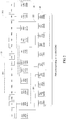
FIG 2 illustrates a schematic diagram of an integrated circuit structure according to an exemplary embodiment of the present disclosure; and -
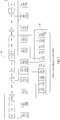
FIG 3 illustrates a schematic diagram of an integrated circuit structure according to another exemplary embodiment of the present disclosure. - Exemplary embodiments will be described more comprehensively by referring to the accompanying drawings now. However, the exemplary embodiments can be embodied in many forms and should not be construed as limited to the embodiments set forth herein; rather, these embodiments are provided so that the present disclosure will be made thorough and complete, and the concept of exemplary embodiments will be fully conveyed to those skilled in the art. Furthermore, the described features, structures, or characteristics may be combined in any suitable manner in one or more embodiments. In the following description, numerous details are provided to provide a thorough understanding of the embodiments of the present disclosure. Those skilled in the art will recognize, however, that the technical solution of the present disclosure may be practiced without one or more of the details described, or that other methods, components, devices, steps and so on may be employed. In other instances, well-known technical solutions are not shown or described in detail to avoid obscuring aspects of the present disclosure.
- In addition, the accompanying drawings are merely exemplary illustration of the present disclosure, and are not necessarily drawn to scale. The same reference numerals in the drawings denote the same or similar parts, and thus repeated description thereof will be omitted.
- In the process of executing a write operation by a memory such as LPDDR4, a DQ input circuit module may obtain a signal transmitted by a data queue (DQ) port, and this signal generally is a signal that cannot be directly processed by a digital circuit due to parasitic effects and various interferences. In this case, the DQ input circuit module needs to sample the obtained DQ signal by means of a DQS signal, and the DQ input circuit module writes results obtained by sampling into a storage array.
- The DQS signal and the DQ signal almost take the same time to reach the LPDDR4, and inside the LPDDR4, it takes a while for the DQS signal to be transmitted to the DQ input circuit module, which causes the DQS signal to be out of sync with the DQ signal. To avoid this situation, a semiconductor memory chip may transmit the DQS signal to the LPDDR4 one tDQS2DQ in advance, such that the DQS signal and the DQ signal can reach the DQ input circuit module synchronously, to improve the accuracy of sampling the DQ signal by the DQ input circuit module.
- However, the tDQS2DQ is susceptible to factors such as internal operating voltage or operating temperature of the LPDDR4. To solve this problem, the tDQS2DQ needs to be adjusted by continuously detecting variations of parameters such as the internal operating voltage, the operating temperature and the like. However, the detection process consumes time and energy, which results in slower write speed, thus having a negative effect on the working performance of the memory.
-
FIG 1 illustrates a schematic diagram of an integrated circuit structure in some technologies. In these technologies, a DQ input/output circuit module and a signal pad are manufactured and configured together, such that a path for the obtained DQS signal to reach the DQ input/output circuit module at two ends is longer, which is approximate to the length of a region occupied by the signal pad. In the case where the DQ includes 8 bits in total from DQ0 to DQ7, if a corresponding signal pad pitch is 60µm, the sum of the paths for the DQS signal to reach DQ0 and DQ7 input/output circuit modules is about 1,140µm. In the exemplary embodiments of the present disclosure, the sum of the paths is denoted as the path corresponding to the tDQS2DQ. - In view of this, if the path corresponding to the tDQS2DQ is shortened, the effects of the factors such as the operating voltage, the operating temperature and the like on the tDQS2DQ are also reduced. In addition, the shortening of the path can also reduce current consumption and help to ensure signal integrity. Thus, the write performance of the memory can be improved.
- An integrated circuit structure in one exemplary embodiment of the present disclosure will be described below with reference to
FIG 2 . - With reference to
FIG 2 , the integrated circuit structure may include apad region 21 and afirst circuit region 22. - The
pad region 21 includes a plurality of signal pads arranged along a target direction, wherein the signal pad refers to a pad corresponding to each data signal port. The signal pad may include but is not limited to a plurality of data input/output pads, a first differential data strobe pad, a second differential data strobe pad, and a data mask pad. - For the plurality of data input/output pads, taking the DQ including 8 bits from DQ0 to DQ7 in total as an example, the plurality of data input/output pads include a DQ0 pad, a DQ1 pad, a DQ2 pad, a DQ3 pad, a DQ4 pad, a DQ5 pad, a DQ6 pad, and a DQ7 pad. However, it is to be understood that the plurality of data input/output pads may also include a total of 16 pads from DQ0 to DQ15, depending on different types of memories, which is not limited in the present disclosure.
- The data input/output pad executes the write operation and the read operation synchronously. In the process of executing the write operation, the data input/output pad receives a data signal from a pin through a lead, and transmits the data signal to a corresponding circuit module. In the process of executing the read operation, the data input/output pad receives the data signal from the corresponding circuit module and transmits this signal through the pin.
- In a memory above DDR4, a differential data strobe pad may include a first differential data strobe pad (denoted as DQS_t pad) and a second differential data strobe pad (denoted as DQS_c pad). A signal received by the first differential data strobe pad and a signal received by the second differential data strobe pad have the same amplitude and opposite phases. In the process of sampling using a differential signal, a time point at which two differential signals cross may be, for example, a time point of sampling, and the data signal is sampled based on this time point of sampling.
- For the data mask pad (DM pad), a mask signal for executing partial write functions may be inputted. When the received mask signal is at a low level, the bit corresponding to the input data will be discarded.
- In addition, the
pad region 21 may also include a plurality of power source pads (VDDQ pads) and a plurality of ground pads (VSSQ pads) to provide power source and ground terminals. - According to one embodiment of the present disclosure, the
pad region 21 may include afirst pad subregion 211 and asecond pad subregion 212. The number of data input/output pads contained in thefirst pad subregion 211 is equal to that of data input/output pads contained in thesecond pad subregion 212, and the number is half of the total number of the data input/output pads. For example, thefirst pad subregion 211 includes a DQ0 pad, a DQ1 pad, a DQ2 pad, and a DQ3 pad; and thesecond pad subregion 212 includes a DQ4 pad, a DQ5 pad, a DQ6 pad, and a DQ7 pad. - In this case, the first differential data strobe pad, the second differential data strobe pad and the data mask pad may be arranged between the
first pad subregion 211 and thesecond pad subregion 212, making it easier for a differential data strobe signal to perform path matching on each DQ input circuit module, thereby avoiding the problem of excessive distance difference. - It is to be understood that according to some other embodiments of the present disclosure, any one of the first differential data strobe pad, the second differential data strobe pad and the data mask pad may be arranged on one side of the
pad region 21, and their positions with respect to each data input/output pad is not limited. - The
first circuit region 22 is arranged on one side of thepad region 21. That is, thefirst circuit region 22 and thepad region 21 are two regions without overlapped regions. Corresponding to the plurality of signal pads in thepad region 21, thefirst circuit region 22 includes a plurality of signal input circuit modules arranged along a target direction, and each of the plurality of signal input circuit modules is connected to a corresponding signal pad through a metal wire. Each of the plurality of signal input circuit modules is configured to implement a sampling operation of an input signal and write a sampling result into a storage array. - The plurality of signal input circuit modules may include a plurality of data input circuit modules, a plurality of data strobe circuit modules, and a plurality of data mask circuit modules.
- For the plurality of data input circuit modules, corresponding to the plurality of data input/output pads described above, the plurality of data input circuit modules may include a DQ0 input circuit module, a DQ1 input circuit module, a DQ2 input circuit module, a DQ3 input circuit module, a DQ4 input circuit module, a DQ5 input circuit module, a DQ6 input circuit module, and a DQ7 input circuit module.
- Each of the plurality of DQ input circuit modules is configured to receive a data signal transmitted by the corresponding DQ pad and sample the data signal in response to a data strobe signal to write the sampling result into the storage array.
- Also be referred to as a data strobe input circuit module in the embodiments of the present disclosure, the data strobe circuit module is configured to transmit the data strobe signal to each of the plurality of DQ input circuit modules.
- The data mask circuit module is configured to obtain mask information and execute corresponding partial write operations.
- According to one embodiment of the present disclosure, the
first circuit region 22 includes afirst circuit subregion 221 and asecond circuit subregion 222. The number of data input circuit modules contained in thefirst circuit subregion 221 is equal to that of data input circuit modules contained in thesecond circuit subregion 222, and the number is half of the total number of the data input circuit modules. For example, thefirst circuit subregion 221 includes a DQ0 input circuit module, a DQ1 input circuit module, a DQ2 input circuit module, and a DQ3 input circuit module. Thesecond circuit subregion 222 includes a DQ4 input circuit module, a DQ5 input circuit module, a DQ6 input circuit module, and a DQ7 input circuit module. - In this case, the data strobe circuit module and the data mask circuit module are arranged between the
first circuit subregion 221 and thesecond circuit subregion 222. - In addition, with reference to
FIG. 2 , the data strobe circuit module may be connected to the first differential data strobe pad and the second differential data strobe pad through metal wires. - In the exemplary embodiments of the present disclosure, a size of the
first circuit region 22 along a target direction is smaller than that of thepad region 21 along the target direction. As mentioned above, the size of thefirst circuit region 22 along the target direction refers to the length of thefirst circuit region 22 along a direction in which a plurality of signal input circuit modules are arranged, i.e., a length of a path corresponding to the tDQS2DQ. - The size of the
first circuit region 22 along the target direction is designed to be less than that of thepad region 21 along the target direction. In one aspect, the length of the path for transmitting the DQS signal to the DQ input circuit module is reduced, and thus the tDQS2DQ is reduced. In another aspect, a shorter path can alleviate the temperature and voltage interferences, which can greatly improve temperature and voltage performances and can reduce current consumption, helping to ensure signal integrity and improve memory performance. - According to some embodiments of the present disclosure, in the
first circuit region 22, a distance between the adjacent signal input circuit modules is smaller than a distance threshold. The distance threshold may be determined based on the size of thepad region 21 along the target direction and the size of each of the plurality of signal input circuit modules along the target direction, such that the size of thefirst circuit region 22 along the target direction is smaller than that of thepad region 21 along the target direction. It is to be noted that distances between the adjacent signal input circuit modules may be the same or may be different. - As illustrated in
FIG 2 , there may be gaps between the adjacent signal input circuit modules to avoid mutual interference between these modules. - In addition, the integrated circuit structure in the exemplary embodiments of the present disclosure further includes a second circuit region 23.
- The second circuit region 23 may be arranged on the same side of the
pad region 21 with respect to thefirst circuit region 22. That is, with respect to thepad region 21, thefirst circuit region 22 and the second circuit region 23 are arranged on the same side. - The second circuit region 23 may include a plurality of signal output circuit modules arranged along the target direction. Each of the plurality of signal output circuit modules is connected to the corresponding one of the plurality of signal pads through metal wires, and each of the plurality of signal output circuit modules is configured to read data stored in the storage array.
- In addition, the size of the first circuit region along the target direction may be set smaller.
- Referring to
FIG 3 , thepad region 31 is the same as thepad region 21 inFIG. 2 , and thus is not to be described again. For thefirst circuit region 32, the distances between the adjacent signal input circuit modules may be as small as possible. That is, the above-mentioned distance threshold may be configured as small as possible. In adjacent structures configured as illustrated inFIG 3 , the length of the path corresponding to the tDQS2DQ is further shortened, and thus more space may be saved in the fabrication processes. - As far as the exemplary structures as illustrated in
FIG 3 is concerned, the path corresponding to the tDQS2DQ is merely about 200µm because each of the plurality of signal input circuit modules has a smaller area. Compared with the 1,140µm in some technologies inFIG 1 , the length of the path is greatly reduced. - In addition, with reference to
FIG 2 orFIG 3 , in the embodiments of the present disclosure, the metal wires from the plurality of pads to the plurality of signal input circuit modules may be configured to be narrow, and thus a large current drive is not required, and input capacitance can be reduced. - The present disclosure also provides a memory, which includes any one of the above-mentioned integrated circuit structures.
- It is to be understood that the present disclosure does not limit the type of the memory, which may be a DDR4 SDRAM such as an LPDDR4 , or may be a DDR5 memory, etc.
- Other embodiments of the present disclosure will be apparent to those skilled in the art from consideration of the specification and practice of the present disclosure disclosed here. This application is intended to cover any variations, uses, or adaptations of the present disclosure following the general principles thereof and including such departures from the present disclosure as come within known or customary practice in the art. It is intended that the specification and embodiments be considered as exemplary only, with a true scope and spirit of the present disclosure being indicated by the following claims.
- It will be appreciated that the present disclosure is not limited to the exact construction that has been described above and illustrated in the accompanying drawings, and that various modifications and changes can be made without departing from the scope thereof. It is intended that the scope of the present disclosure only be limited by the appended claims.
Claims (10)
- An integrated circuit structure, comprising:a pad region comprising a plurality of signal pads arranged along a target direction; anda first circuit region arranged on one side of the pad region, the first circuit region comprising a plurality of signal input circuit modules arranged along the target direction and correspondingly connected to the plurality of signal pads respectively, each of the plurality of signal input circuit modules being configured to implement a sampling operation of an input signal and write a sampling result into a storage array; and, wherein a size of the first circuit region along the target direction is smaller than that of the pad region along the target direction.
- The integrated circuit structure of claim 1, wherein each of the plurality of signal pads comprises:
a first differential data strobe pad, a second differential data strobe pad, a data mask pad, and a plurality of data input/output pads. - The integrated circuit structure of claim 2, wherein the pad region further comprises:
a plurality of power source pads and a plurality of ground pads. - The integrated circuit structure of claim 2, wherein the pad region comprises:a first pad subregion and a second pad subregion, the first pad subregion and the second pad subregion comprising an equal number of data input/output pads, and the number being half of a total number of data input/output pads;wherein the first differential data strobe pad, the second differential data strobe pad and the data mask pad are arranged between the first pad subregion and the second pad subregion.
- The integrated circuit structure of claim 4, wherein each of the plurality of signal input circuit modules comprises:
a data strobe circuit module, a data mask circuit module, and a plurality of data input circuit modules. - The integrated circuit structure of claim 5, wherein the first circuit region comprises:a first circuit subregion and a second circuit subregion, the first circuit subregion and the second circuit subregion comprising an equal number of data input circuit modules, and the number being half of a total number of data input circuit modules;wherein the data strobe circuit module and the data mask circuit module are arranged between the first circuit subregion and the second circuit subregion.
- The integrated circuit structure of claim 5, wherein the data strobe circuit module is connected to the first differential data strobe pad and the second differential data strobe pad, respectively.
- The integrated circuit structure of any one of claims 1 to 7, wherein a distance between adjacent signal input circuit modules is less than a distance threshold; and
wherein the distance threshold is determined based on a size of the pad region along the target direction and a size of each of the plurality of signal input circuit modules along the target direction. - The integrated circuit structure of claim 1, further comprising:
a second circuit region arranged on same side of the pad region with respect to the first circuit region, the second circuit region comprising a plurality of signal output circuit modules arranged along the target direction and correspondingly connected to the plurality of signal pads respectively, each of the plurality of signal output circuit modules being configured to read data stored in the storage array. - A memory, comprising the integrated circuit structure of any one of claims 1 to 9.
Applications Claiming Priority (3)
| Application Number | Priority Date | Filing Date | Title |
|---|---|---|---|
| CN202020081378.XU CN210805229U (en) | 2020-01-14 | 2020-01-14 | Integrated circuit structure and memory |
| CN202010036731.7A CN113192541B (en) | 2020-01-14 | 2020-01-14 | Integrated circuit structure and memory |
| PCT/CN2020/099980 WO2021143069A1 (en) | 2020-01-14 | 2020-07-02 | Integrated circuit structure and memory |
Publications (2)
| Publication Number | Publication Date |
|---|---|
| EP3905247A1 true EP3905247A1 (en) | 2021-11-03 |
| EP3905247A4 EP3905247A4 (en) | 2022-04-06 |
Family
ID=76863913
Family Applications (1)
| Application Number | Title | Priority Date | Filing Date |
|---|---|---|---|
| EP20914003.7A Ceased EP3905247A4 (en) | 2020-01-14 | 2020-07-02 | IC STRUCTURE AND MEMORY |
Country Status (3)
| Country | Link |
|---|---|
| US (1) | US11450361B2 (en) |
| EP (1) | EP3905247A4 (en) |
| WO (1) | WO2021143069A1 (en) |
Family Cites Families (10)
| Publication number | Priority date | Publication date | Assignee | Title |
|---|---|---|---|---|
| JP4309368B2 (en) * | 2005-03-30 | 2009-08-05 | エルピーダメモリ株式会社 | Semiconductor memory device |
| US7359252B2 (en) * | 2006-01-09 | 2008-04-15 | Infineon Technologies Ag | Memory data bus structure and method of transferring information with plural memory banks |
| KR101229612B1 (en) | 2011-03-28 | 2013-02-04 | 이상화 | Portable reading stand |
| US20130318393A1 (en) * | 2011-11-15 | 2013-11-28 | Ocz Technology Group Inc. | Solid-state mass storage device and methods of operation |
| JP2013118033A (en) * | 2011-12-05 | 2013-06-13 | Elpida Memory Inc | Semiconductor device |
| US9213487B2 (en) * | 2013-10-16 | 2015-12-15 | Qualcomm Incorporated | Receiver architecture for memory reads |
| US10020252B2 (en) * | 2016-11-04 | 2018-07-10 | Micron Technology, Inc. | Wiring with external terminal |
| CN108417231A (en) * | 2018-02-28 | 2018-08-17 | 四川斐讯信息技术有限公司 | A kind of the line length detection method and system of DDR wirings |
| CN210805229U (en) * | 2020-01-14 | 2020-06-19 | 长鑫存储技术(上海)有限公司 | Integrated circuit structure and memory |
| CN210805230U (en) * | 2020-01-14 | 2020-06-19 | 长鑫存储技术有限公司 | Integrated Circuit Structures and Memories |
-
2020
- 2020-07-02 WO PCT/CN2020/099980 patent/WO2021143069A1/en not_active Ceased
- 2020-07-02 EP EP20914003.7A patent/EP3905247A4/en not_active Ceased
-
2021
- 2021-04-28 US US17/243,461 patent/US11450361B2/en active Active
Also Published As
| Publication number | Publication date |
|---|---|
| US11450361B2 (en) | 2022-09-20 |
| EP3905247A4 (en) | 2022-04-06 |
| US20210249056A1 (en) | 2021-08-12 |
| WO2021143069A1 (en) | 2021-07-22 |
Similar Documents
| Publication | Publication Date | Title |
|---|---|---|
| CN210805230U (en) | Integrated Circuit Structures and Memories | |
| CN210805229U (en) | Integrated circuit structure and memory | |
| US7391634B2 (en) | Semiconductor memory devices having controllable input/output bit architectures | |
| US7969193B1 (en) | Differential sensing and TSV timing control scheme for 3D-IC | |
| US20260080931A1 (en) | Memory devices configured to provide external regulated voltages | |
| WO2021034431A1 (en) | Methods for providing device status in response to read commands directed to write-only mode register bits and memory devices and systems employing the same | |
| US11789890B2 (en) | Memory devices, modules and systems having memory devices with varying physical dimensions, memory formats, and operational capabilities | |
| US6111795A (en) | Memory device having row decoder | |
| US11514959B2 (en) | Memory device capable of adjusting clock signal based on operating speed and propagation delay of command/address signal | |
| EP4027345B1 (en) | Transmission circuit, interface circuit and memory | |
| US6594167B1 (en) | Semiconductor integrated circuit having a structure for equalizing interconnection lengths and memory module provided with the semiconductor integrated circuit | |
| US20210103533A1 (en) | Memory system and memory chip | |
| CN110875065B (en) | DRAM sense amplifier active matching fill features for gap equivalence systems and methods | |
| US11450361B2 (en) | Integrated circuit structure and memory | |
| CN113129942A (en) | Integrated circuit structure and memory | |
| US11367478B2 (en) | Integrated circuit structure and memory | |
| EP3923285B1 (en) | Integrated circuit structure and memory | |
| JP2002158295A (en) | Semiconductor device | |
| KR102702110B1 (en) | Centralized placement of commands and addresses in memory devices | |
| CN113192541B (en) | Integrated circuit structure and memory | |
| US11545200B1 (en) | Data control circuit for increasing maximum and minimum tolerance values of skew between DQS signal and clock signal during write operation and associated memory device | |
| JP2003332467A (en) | Semiconductor device | |
| WO2021143050A1 (en) | Integrated circuit structure and memory | |
| US20250359033A1 (en) | Silicon On Insulator Device with Floating Body Effect Mitigation | |
| US20070090500A1 (en) | Housed DRAM chip for high-speed applications |
Legal Events
| Date | Code | Title | Description |
|---|---|---|---|
| STAA | Information on the status of an ep patent application or granted ep patent |
Free format text: STATUS: THE INTERNATIONAL PUBLICATION HAS BEEN MADE |
|
| PUAI | Public reference made under article 153(3) epc to a published international application that has entered the european phase |
Free format text: ORIGINAL CODE: 0009012 |
|
| STAA | Information on the status of an ep patent application or granted ep patent |
Free format text: STATUS: REQUEST FOR EXAMINATION WAS MADE |
|
| 17P | Request for examination filed |
Effective date: 20210729 |
|
| AK | Designated contracting states |
Kind code of ref document: A1 Designated state(s): AL AT BE BG CH CY CZ DE DK EE ES FI FR GB GR HR HU IE IS IT LI LT LU LV MC MK MT NL NO PL PT RO RS SE SI SK SM TR |
|
| A4 | Supplementary search report drawn up and despatched |
Effective date: 20220303 |
|
| RIC1 | Information provided on ipc code assigned before grant |
Ipc: G11C 7/04 20060101ALI20220225BHEP Ipc: G11C 7/02 20060101ALI20220225BHEP Ipc: G11C 11/4093 20060101ALI20220225BHEP Ipc: G11C 7/10 20060101ALI20220225BHEP Ipc: G11C 5/02 20060101AFI20220225BHEP |
|
| STAA | Information on the status of an ep patent application or granted ep patent |
Free format text: STATUS: EXAMINATION IS IN PROGRESS |
|
| 17Q | First examination report despatched |
Effective date: 20230119 |
|
| DAV | Request for validation of the european patent (deleted) | ||
| DAX | Request for extension of the european patent (deleted) | ||
| REG | Reference to a national code |
Ref country code: DE Ref legal event code: R003 |
|
| STAA | Information on the status of an ep patent application or granted ep patent |
Free format text: STATUS: THE APPLICATION HAS BEEN REFUSED |
|
| 18R | Application refused |
Effective date: 20240121 |