EP3905036A1 - Reconfigurable circuit, corresponding device, system and method - Google Patents
Reconfigurable circuit, corresponding device, system and method Download PDFInfo
- Publication number
- EP3905036A1 EP3905036A1 EP21168368.5A EP21168368A EP3905036A1 EP 3905036 A1 EP3905036 A1 EP 3905036A1 EP 21168368 A EP21168368 A EP 21168368A EP 3905036 A1 EP3905036 A1 EP 3905036A1
- Authority
- EP
- European Patent Office
- Prior art keywords
- circuit
- input
- signal
- circuits
- output
- Prior art date
- Legal status (The legal status is an assumption and is not a legal conclusion. Google has not performed a legal analysis and makes no representation as to the accuracy of the status listed.)
- Granted
Links
Images


Classifications
-
- G—PHYSICS
- G06—COMPUTING OR CALCULATING; COUNTING
- G06F—ELECTRIC DIGITAL DATA PROCESSING
- G06F7/00—Methods or arrangements for processing data by operating upon the order or content of the data handled
- G06F7/38—Methods or arrangements for performing computations using exclusively denominational number representation, e.g. using binary, ternary, decimal representation
- G06F7/48—Methods or arrangements for performing computations using exclusively denominational number representation, e.g. using binary, ternary, decimal representation using non-contact-making devices, e.g. tube, solid state device; using unspecified devices
- G06F7/4806—Computations with complex numbers
-
- G—PHYSICS
- G06—COMPUTING OR CALCULATING; COUNTING
- G06F—ELECTRIC DIGITAL DATA PROCESSING
- G06F13/00—Interconnection of, or transfer of information or other signals between, memories, input/output devices or central processing units
- G06F13/14—Handling requests for interconnection or transfer
- G06F13/16—Handling requests for interconnection or transfer for access to memory bus
- G06F13/1668—Details of memory controller
-
- G—PHYSICS
- G06—COMPUTING OR CALCULATING; COUNTING
- G06F—ELECTRIC DIGITAL DATA PROCESSING
- G06F13/00—Interconnection of, or transfer of information or other signals between, memories, input/output devices or central processing units
- G06F13/14—Handling requests for interconnection or transfer
- G06F13/20—Handling requests for interconnection or transfer for access to input/output bus
- G06F13/28—Handling requests for interconnection or transfer for access to input/output bus using burst mode transfer, e.g. direct memory access DMA, cycle steal
-
- G—PHYSICS
- G06—COMPUTING OR CALCULATING; COUNTING
- G06F—ELECTRIC DIGITAL DATA PROCESSING
- G06F13/00—Interconnection of, or transfer of information or other signals between, memories, input/output devices or central processing units
- G06F13/38—Information transfer, e.g. on bus
- G06F13/40—Bus structure
- G06F13/4004—Coupling between buses
- G06F13/4027—Coupling between buses using bus bridges
-
- G—PHYSICS
- G06—COMPUTING OR CALCULATING; COUNTING
- G06F—ELECTRIC DIGITAL DATA PROCESSING
- G06F7/00—Methods or arrangements for processing data by operating upon the order or content of the data handled
- G06F7/38—Methods or arrangements for performing computations using exclusively denominational number representation, e.g. using binary, ternary, decimal representation
- G06F7/48—Methods or arrangements for performing computations using exclusively denominational number representation, e.g. using binary, ternary, decimal representation using non-contact-making devices, e.g. tube, solid state device; using unspecified devices
- G06F7/50—Adding; Subtracting
-
- G—PHYSICS
- G06—COMPUTING OR CALCULATING; COUNTING
- G06F—ELECTRIC DIGITAL DATA PROCESSING
- G06F7/00—Methods or arrangements for processing data by operating upon the order or content of the data handled
- G06F7/38—Methods or arrangements for performing computations using exclusively denominational number representation, e.g. using binary, ternary, decimal representation
- G06F7/48—Methods or arrangements for performing computations using exclusively denominational number representation, e.g. using binary, ternary, decimal representation using non-contact-making devices, e.g. tube, solid state device; using unspecified devices
- G06F7/52—Multiplying; Dividing
- G06F7/523—Multiplying only
Definitions
- the description relates to digital signal processing circuits, such as hardware accelerators, and related devices and systems.
- a variety of real-time digital signal processing systems may involve processing a relevant amount of data per unit of time.
- processing may turn out to be highly demanding for purely core-based implementations (i.e., implementations involving general purpose microprocessors or microcontrollers running processing software).
- processing elements also referred to as “mathematical units” or “mathematical operators”
- processing elements may comprise multiply-and-accumulate (MAC) circuits and/or circuits configured to compute activation functions such as activation non-linear functions, ANLF (e.g., coordinate rotation digital computer, CORDIC, circuits).
- MAC multiply-and-accumulate
- ANLF e.g., coordinate rotation digital computer, CORDIC, circuits
- Each of the above-mentioned processing elements is typically designed for implementing a specific function (e.g., a radix-2 butterfly algorithm, a multiplication of complex vectors, a vector/matrix product, a trigonometric or exponential or logarithmic function, a convolution, etc.). Therefore, a conventional hardware accelerator typically comprises a variety of such different processing elements connected together through some kind of interconnect network. In some cases, the various processing elements are activated one at a time due to data dependencies and/or architecture limitations, leading to an inefficient usage of silicon area and of the available hardware resources.
- a specific function e.g., a radix-2 butterfly algorithm, a multiplication of complex vectors, a vector/matrix product, a trigonometric or exponential or logarithmic function, a convolution, etc.
- a purely software-implemented, core-based approach may involve high clock frequencies in order to satisfy the typical bandwidth requirements of real-time systems, since in such case each processing element executes basic operations.
- An object of one or more embodiments is that of providing a hardware accelerator device which solves one or more of the above mentioned drawbacks.
- one or more embodiments aim at providing a memory-based hardware accelerator device (also referred to with the acronym EDPA, Enhanced Data Processing Architecture, in the context of the present disclosure) comprising one or more processing elements.
- the processing elements in the hardware accelerator device may be reconfigurable, possibly at run time, so to provide increased flexibility of use and facilitate efficient computation of a variety of signal processing operations which may be particularly demanding in terms of resources (e.g., Fast Fourier Transform, digital filtering, implementation of artificial neural networks, etc.).
- One or more embodiments may find application in real-time processing systems in which the acceleration of computationally demanding operations (e.g., vector/matrix product, convolution, FFT, radix-2 butterfly algorithm, multiplication of complex vectors, trigonometric or exponential or logarithmic function, etc.) may facilitate meeting certain performance requirements (e.g., in terms of processing time). This may be the case, for instance, in the automotive field.
- computationally demanding operations e.g., vector/matrix product, convolution, FFT, radix-2 butterfly algorithm, multiplication of complex vectors, trigonometric or exponential or logarithmic function, etc.
- such an object can be achieved by means of a circuit (e.g., a runtime reconfigurable processing unit) having the features set forth in the claims that follow.
- a circuit e.g., a runtime reconfigurable processing unit
- One or more embodiments may relate to a corresponding device (e.g., a hardware accelerator circuit comprising one or more runtime reconfigurable processing units).
- a corresponding device e.g., a hardware accelerator circuit comprising one or more runtime reconfigurable processing units.
- One or more embodiments may relate to a corresponding system (e.g., a system-on-chip integrated circuit comprising a hardware accelerator circuit).
- a corresponding system e.g., a system-on-chip integrated circuit comprising a hardware accelerator circuit.
- One or more embodiments may relate to a corresponding method.
- a circuit which may comprise a set of input terminals configured to receive input digital signals which carry input data, and a set of output terminals configured to provide output digital signals which carry output data.
- the circuit may comprise computing circuitry configured to produce said output data as a function of said input data.
- the computing circuitry may comprise a set of multiplier circuits, a set of adder-subtractor circuits, a set of accumulator circuits, and a configurable interconnect network.
- the configurable interconnect network may be configured to selectively couple the multiplier circuits, the adder-subtractor circuits, the accumulator circuits, the input terminals and the output terminals in at least two processing configurations.
- the computing circuitry may be configured to compute said output data according to a first set of functions, and in at least one second processing configuration, the computing circuitry may be configured to compute said output data according to a respective second set of functions.
- the second set of functions is different from the first set of functions.
- One or more embodiments may thus provide increased flexibility, improved usage of hardware resources, and/or improved performance for parallel computation.
- references to "an embodiment” or “one embodiment” in the framework of the present description is intended to indicate that a particular configuration, structure, or characteristic described in relation to the embodiment is comprised in at least one embodiment.
- phrases such as “in an embodiment” or “in one embodiment” that may be present in one or more points of the present description do not necessarily refer to one and the same embodiment.
- particular conformations, structures, or characteristics may be combined in any adequate way in one or more embodiments.
- FIG. 1 is exemplary of an electronic system 1 according to one or more embodiments, such as a system-on-chip (SoC).
- the electronic system 1 may comprise various electronic circuits such as, for instance: a central processing unit 10 (CPU, e.g., a microprocessor), a main system memory 12 (e.g., a system RAM - Random Access Memory), a direct memory access (DMA) controller 14, and a hardware accelerator device 16.
- CPU central processing unit
- main system memory 12 e.g., a system RAM - Random Access Memory
- DMA direct memory access
- the electronic circuits in the electronic system 1 may be connected by means of a system interconnect network 18, e.g., a SoC interconnect.
- a system interconnect network e.g., a SoC interconnect.
- One or more embodiments may thus facilitate improving usage of silicon area and providing satisfactory processing performance, e.g., to satisfy the processing time requirements of real-time data processing systems.
- the hardware accelerator circuit 16 may further comprise a local control unit 161, a local interconnect network 162, a local data memory controller 163, a local ROM controller 164 coupled to a set of local read-only memories 165, preferably a number P of local read-only memories 165 0 , 165 1 , ..., 165 P-1 , and a local configuration memory controller 166 coupled to a set of local configurable coefficient memories 167, preferably a number P of local configurable coefficient memories 167 0 , 167 1 , ..., 167 P-1 .
- the memories 167 may comprise volatile memories (e.g., RAM memories) and/or non-volatile memories (e.g., PCM memories).
- Different embodiments may comprise a different number P of processing elements 160 and/or a different number Q of local data memory banks Mo, ..., M Q-1 .
- P may be equal to 8 and Q may be equal to 16.
- the processing elements 160 may be configurable so as to support different (basic) processing functions with different levels of computational parallelism.
- a processing element 160 may support (e.g., based on a proper static configuration) different types of arithmetic (e.g., floating point single precision 32 bits, fixed-point/integer 32 bits, or 16 or 8 bits with parallel computation or vectored mode).
- the processing elements 160 may comprise respective internal direct memory access (DMA) controllers 168 0 , 168 1 , ..., 168 P-1 having a low complexity.
- a processing element 160 may be configured to retrieve input data from the local data memory banks Mo, ..., M Q-1 and/or from the main system memory 12 through the respective direct memory access controller 168.
- the processing element 160 may thus elaborate the retrieved input data to generate processed output data.
- the processing element 160 may be configured to store the processed output data in the local data memory banks M 0 , ..., M Q-1 and/or in the main system memory 12 through the respective direct memory access controller 168.
- processing elements 160 may be configured to retrieve input data from the local read-only memory 165 and/or from the local configurable coefficient memory 167 to perform such elaboration.
- providing a set of local data memory banks M 0 , ..., M Q-1 may facilitate processing data in parallel and reducing memory access conflicts.
- the local data memory banks Mo, ..., M Q-1 may be provided with buffering (e.g., double buffering) which may facilitate recovering the memory upload time (write operation) and/or download time (read operation).
- each local data memory bank may be duplicated, so that data can be read (e.g., for being processed) from one of the two memory banks and (new) data can be stored (e.g., for being processed later) in the other memory bank at the same time.
- moving data may not negatively affect computation performances, as it may be masked.
- a double buffering scheme of the local data memory banks Mo, ..., M Q-1 may be advantageous in combination with data processing in streaming mode or back to back (e.g., as applicable to a FFT N-point processor that is configured to elaborate continuous sequences of N data inputs).
- the local data memory banks M 0 , ..., M Q-1 may comprise memory banks having a limited storage capacity (and thus, a limited silicon footprint).
- each of the local data memory banks may have a storage capacity of at least (maxN)/Q, where maxN is the longest FFT that the hardware is able to handle.
- maxN is the longest FFT that the hardware is able to handle.
- the local control unit 161 may comprise a register file including information for setting up the configuration of the processing elements 160. For instance, the local control unit 161 may set up the processing elements 160 to perform a specific algorithm as directed by a host application running on the central processing unit 10.
- the local control unit 161 may thus comprise a controller circuit of the hardware accelerator circuit 16.
- a controller circuit may configure (e.g., dynamically) each of the processing elements 160 for computing a specific (basic) function, and may configure each of the respective internal direct memory access controllers 168 with a specific memory access scheme and loop cycle.
- the local interconnect network 162 may comprise a low complexity interconnect system, e.g., based on a bus network of a known type such as an AXI4-based interconnect.
- the data parallelism of the local interconnect network 162 may be on 64 bits and the address width may be 32 bits.
- the local interconnect network 162 may be configured to connect the processing elements 160 to the local data memory banks Mo, ..., M Q-1 and/or to the main system memory 12. Additionally, the local interconnect network 162 may be configured to connect the local control unit 161 and the local configuration memory controller 166 to the system interconnect network 18.
- the interconnect network 162 may comprise:
- the interconnect network 162 may be fixed (i.e., not reconfigurable).
- the interconnect network 162 may implement the following connections:
- Table I-1 summarizes such exemplary connections implemented by means of the interconnect network 162.
- the interconnect network 162 may further implement the following connections: each of the P master ports MP 0 , MP 1 , ..., MP P-1 may be connected to the system slave port SPp coupled to the system interconnect network 18. In this way, connectivity may be provided between any processing element 160 and the SoC via the system interconnect network 18.
- Table 1-2 summarizes such exemplary connections implemented by means of the interconnect network 162.
- the interconnect network 162 may further implement the following connection: the system master port MPp coupled to the system interconnect network 18 may be connected to at least one of the slave ports SP 0 , SP 1 , ..., SP P-1 (here, the first slave port SP 0 in the set of P slave ports SP 0 , SP 1 , ..., SP P-1 ). In this way, connection may be provided between the master port MPp and (any) slave.
- connection of the master port MPp may be extended to a plurality of (e.g., all) the slave ports SP 0 , SP 1 , ..., SP P-1 .
- Connection of the master port MP P to at least one of the slave ports SP 0 , SP 1 , ..., SP P-1 may be used (only) to load the input data to be processed into the local data memory banks Mo, ..., M Q-1 , insofar as all memory banks may be accessed via a single slave port.
- Loading input data can be done using only one slave port, while processing said data by means of parallel computation may take advantage of using a plurality (e.g., all) of the slave ports SP 0 , SP 1 , ..., SP P-1 .
- Table 1-3 summarizes such exemplary connections implemented by means of the interconnect network 162.
- the local data memory controller 163 may be configured to arbitrate access (e.g., by the processing elements 160) to the local data memory banks M 0 , ..., M Q-1 .
- the local data memory controller 163 may use memory access schemes selectable as a function of a signal received from the local control unit 161 (e.g., for computation of a specific algorithm).
- the local data memory controller 163 may translate input read/write transaction bursts (e.g., AXI bursts) generated by the read/write direct memory access controllers 168 into a sequence of read/write memory accesses, according to a specified burst type, burst length and memory access scheme.
- input read/write transaction bursts e.g., AXI bursts
- one or more embodiments of a hardware accelerator circuit 16 as exemplified in Figure 1 may aim at reducing the complexity of the local interconnect network 162 by delegating to the local data memory controller 163 the implementation of the (reconfigurable) connections between the processing elements and the local data memory banks.
- the local read-only memories 165 0 , 165 1 , ..., 165 P-1 accessible by the processing elements 160 via the local ROM controller 164 may be configured to store numeric factors and/or fixed coefficients for implementation of specific algorithms or operations (for instance, twiddle factors for FFT computation or other complex coefficients).
- the local ROM controller 164 may implement specific address schemes.
- the local configurable coefficient memories 167 0 , 167 1 , ..., 167 P-1 accessible by the processing elements 160 via the local configuration memory controller 166 may be configured to store application-dependent numeric factors and/or coefficients which can be configured by software (for instance, coefficients for implementing a FIR filter or a beamforming operation, weights of a neural network, etc.).
- the local configuration memory controller 166 may implement specific address schemes.
- the local read-only memories 165 0 , 165 1 , ..., 165 P-1 and/or the local configurable coefficient memories 167 0 , 167 1 , ..., 167 P-1 may advantageously be split into a number P of banks equal to the number of processing elements 160 comprised in the hardware accelerator circuit 16. This may facilitate avoiding conflicts during parallel computations.
- each of the local configurable coefficient memories may be configured to provide in parallel the full set of coefficients required for each processing element 160.
- Figure 2 is a circuit block diagram exemplary of one or more embodiments of a processing element 160 and related connections to the local ROM controller 164, the local configuration memory controller 166, and the local data memory banks M 0 , ..., M Q-1 (with the dotted lines schematically indicating a reconfigurable connection between the processing element 160 and the local data memory banks M 0 , ..., M Q-1 via the local interconnect network 162 and the local data memory controller 163).
- a processing element 160 as exemplified in Figure 2 may be configured to receive:
- a processing element 160 may comprise a number of read direct memory access 200 equal to the number of input signals P, Q.
- the processing element 160 may comprise a computing circuit 20 configurable (possibly at runtime) to process the input values P, Q and the input coefficients W0, W1, W2, W3, W4 to produce a first output signal X0 (e.g., a digital signal indicative of a binary value to be stored in a local data memory bank M 0 , ..., M Q-1 via a respective write direct memory access 204o and buffer register 206 0 such as a FIFO register) and a second output signal X1 (e.g., a digital signal indicative of a binary value to be stored in a local data memory bank M 0 , ..., M Q-1 via a respective write direct memory access 204 1 and buffer register 206 1 such as a FIFO register).
- a first output signal X0 e.g., a digital signal indicative of a binary value to be stored in a local data memory bank M 0 , ..., M Q-1 via a respective write direct memory access 204o and buffer register 206
- a processing element 160 may comprise a number of write direct memory access 204 equal to the number of output signals X0, X1.
- programming of the read and/or write direct memory access 200, 204 may be performed via an interface (e.g., an AMBA interface), which may allow to access internal control registers located in the local control unit 161.
- an interface e.g., an AMBA interface
- a processing element 160 may comprise a ROM address generator circuit 208 coupled to the local ROM controller 164 and a memory address generator circuit 210 coupled to the local configuration memory controller 166 to manage data retrieval therefrom.
- Figure 3 is a circuit block diagram exemplary of a computing circuit 20 as possibly included in one or more embodiments of a processing element 160.
- a computing circuit 20 may comprise a set of processing resources including, for instance, four complex/real multiplier circuits (30a, 30b, 30c, 30d), two complex adder-subtractor circuits (32a, 32b) and two accumulator circuits (34a, 34b) reconfigurably couplable as substantially illustrated in Figure 3 .
- reconfigurable coupling of the processing resources to form different datapaths, with different datapaths corresponding to different mathematical operations may be obtained by means of multiplexer circuits (e.g., 36a to 36j), with each multiplexer receiving a respective control signal (e.g., S0 to S7).
- the multiplier circuits 30a, 30b, 30c, 30d may be configured (e.g., by means of internal multiplexer circuits not visible in the Figures) to operate according to two different configurations selectable as a function of a control signal S8 provided thereto.
- a multiplier may compute the result of two real products on four real operands per clock cycle (i.e., each of the input signals carries two values which are both real values).
- a multiplier may compute the result of one complex product on two complex operands per clock cycle (i.e., each of the input signals carries two values, where a first value is the real part of the operand and the second value is the imaginary part of the operand).
- Table II provided at the end of the description summarizes the exemplary possible configurations of the multiplier circuits 30a, 30b, 30c, 30d.
- processing resources may be arranged as described in the following.
- a first multiplier 30a may receive a first input signal W1 and a second input signal P (e.g., complex operands).
- a third multiplier 30c may receive a first input signal selected out of the output signal from the first multiplier 30a and the input signal P.
- the third multiplier 30c may receive a second input signal selected out of the input signal W3, the input signal W4 and the input signal W0.
- a fourth multiplier 30d may receive a first input signal selected out of the input signal Q and the output signal from the second multiplier 30b.
- the fourth multiplier 30d may receive a second input signal selected out of the input signal W4 and the input signal W0.
- the second input of the fourth multiplier 30d may be coupled to the output of the fourth multiplexer 36d.
- a first adder-subtractor 32a may receive a first input signal selected out of the output signal from the first multiplier 30a, the input signal P and the output signal from the third multiplier 30c.
- the first adder-subtractor 32a may receive a second input signal selected out of the input signal Q, the output from the second multiplier 30b and a null signal (i.e., a binary signal equal to zero).
- a first AND gate 38a may receive as first input signal the output signal from the eighth multiplexer 36h, and as second input signal a control signal G0. The output of the first AND gate 38a may be coupled to the second input of the first adder-subtractor 32a.
- a second adder-subtractor 32b may receive a first input signal selected out of the output signal from the third multiplier 30c and the output signal from the fourth multiplier 30d.
- the second adder-subtractor 32b may receive a second input signal selected out of the output from the fourth multiplier 30d, the output from the second multiplier 30b and a null signal (i.e., a binary signal equal to zero).
- a second AND gate 38b may receive as first input signal the output signal from the tenth multiplexer 36j, and as second input signal a control signal G1. The output of the second AND gate 38b may be coupled to the second input of the second adder-subtractor 32b.
- a first accumulator 34a may receive an input signal from the output of the first adder-subtractor 32a, and a control signal EN, to provide the first output signal X0 of the computing circuit 20.
- a second accumulator 34b may receive an input signal from the output of the second adder-subtractor 32b, and a control signal EN, to provide the second output signal X1 of the computing circuit 20.
- One or more embodiments comprising the adder-subtractors 32a, 32b may retain the capability of "bypassing" their operation by means of the AND gates 38a, 38b which may be used to force a null signal at the second input of the adder-subtractors 32a, 32b.
- Figure 4 is a circuit block diagram exemplary of other embodiments of a computing circuit 20 as possibly included in one or more embodiments of a processing element 160.
- One or more embodiments as exemplified in Figure 4 may comprise the same arrangement of processing resources and multiplexer circuits as discussed with reference to Figure 3 , with the addition of two circuits 40a, 40b configured to compute activation non-linear functions (ANLF), and respective multiplexer circuits 36k, 36m.
- ANLF activation non-linear functions
- the additional processing resources 40a, 40b may be arranged as described in the following.
- a first ANLF circuit 40a may receive an input signal from the output of the first accumulator 34a.
- a second ANLF circuit 40b may receive an input signal from the output of the second accumulator 34b.
- the ANLF circuits 40a and 40b may be "bypassed" by means of the multiplexer circuits 36k and 36m, thereby providing an operation similar to embodiments as exemplified in Figure 3 .
- the datapaths in the computing circuit 20 may be configured to support parallel computation and may facilitate execution of different functions.
- the internal pipeline may be designed to meet timing constraints (e.g., clock frequency) versus a minimum latency.
- the computing circuit 20 is configured to compute an algorithm-dependent (basic) function.
- a single processing element 160 can be programmed to implement a radix-2 DIF (Decimation In Frequency) butterfly algorithm performing the following complex operations, e.g., using signals coming from the internal control unit 161:
- X 0 P + Q
- X 1 P * W 0 ⁇ Q * W 0 where W0 may be a twiddle factor stored inside a local read-only memory 165.
- the input signals (P, Q, W0, W1, W2, W3, W4) and the output signals (X0, X1) may be complex data type.
- a windowing function can be applied to the input data before computing the FFT algorithm.
- Such windowing processing may be supported by the processing element 160, e.g., by making use of four multiplier circuits.
- the module or phase of the spectrum component can be used in the place of the complex value (e.g., in applications such as radar target detection).
- the internal (optional) ANLF circuits can be used during the last FFT stage. For instance, it is possible to rotate the input complex vector so that it is aligned with the x-axis to compute the module.
- Table III provided at the end of the description summarizes some exemplary configurations of the computing circuit 20 for computing different radix-2 algorithms.
- the configuration corresponding to the function "Rdx-2 Butterfly" may involve using two multiplier circuits, two adder-subtractor circuits, no accumulators and no ANLF circuits.
- the configuration corresponding to the function "Rdx-2 Butterfly + windowing" may involve using four multiplier circuits, two adder-subtractor circuits, no accumulators and no ANLF circuits.
- the configuration corresponding to the function "Rdx-2 Butterfly + module” may involve using two multiplier circuits, two adder-subtractor circuits, no accumulators and two ANLF circuits.
- a hardware accelerator circuit 16 may be demanded to compute a scalar product of complex data vectors. For instance, this may be the case of applications involving a filtering operation, such as phased-array radar systems involving a processing stage called beamforming. Beamforming may facilitate a radar system to resolve targets also in the angular (azimuth) dimension, besides the range and radial velocity ones.
- the input signals (P, Q, W0, W1, W2, W3, W4) and the output signals (X0, X1) may be complex data type.
- two different scalar vector product operations may be concurrently carried out by a single processing element 160, e.g., by making use of all the internal hardware resources.
- the local configurable coefficient memory 167 may be used to store the phase shifts for the different array antenna elements.
- an ANLF circuit may be optionally used if a module is to be computed instead of a complex value.
- Table IV provided at the end of the description exemplifies possible configurations of the computing circuit 20 for computing concurrently two scalar products of vectors.
- the configuration corresponding to the function "scalar product of vectors" may involve using four multiplier circuits, two adder-subtractor circuits, two accumulators and no ANLF circuits.
- the configuration corresponding to the function "scalar product of vectors + module" may involve using four multiplier circuits, two adder-subtractor circuits, two accumulators and two ANLF circuits.
- a hardware accelerator circuit 16 may be demanded to compute a scalar product of real data vectors on large real data structures, e.g., for the computation of a digital filter.
- a real-world (e.g., analog) signal may be subject to filtering after having been digitalized, in order to extract (only) the relevant information.
- a convolution operation between an input signal and a filter impulse response may take the form of a scalar product of two real data vectors.
- One of the two vectors may hold the input data, while the other one may hold the coefficients that define the filtering operation.
- the input signals (P, Q, W0, W1, W2, W3, W4) and the output signals (X0, X1) are real data type.
- two different filtering operations may be concurrently carried out by a single processing element 160 on the same data set, processing four different input data per clock cycle, e.g., by making use of all the internal hardware resources.
- Table V provided at the end of the description exemplifies a possible configuration of the computing circuit 20 for computing concurrently two filtering operations on real data vectors.
- the configuration corresponding to the function "scalar product of real vectors" may involve using four multiplier circuits, two adder-subtractor circuits, two accumulators and no ANLF circuits.
- Multilayer Perceptron is a class of fully-connected feedforward artificial neural networks, which may comprise at least three layers of nodes/neurons. Each neuron, except the ones in the input layer, computes a weighted sum of all the nodes in the previous layer and then applies a non-linear activation function to the result.
- a processing element 160 as disclosed herein may handle such non-linear functions, e.g., using the internal ANLF circuits.
- neural networks deal with data coming from the real world and use real weights and functions to compute class membership probabilities (the outputs of the last layer). Real data scalar products may thus be the most computationally demanding and most frequently used operations for such kind of artificial networks.
- Figure 5 is a diagram exemplary of a typical structure of a Multilayer Perceptron network 50.
- a Multiplayer Perceptron network 50 may include:
- a Multilayer Perceptron network may comprise more than one hidden layer 50b.
- a Multiplayer Perceptron network 50 may include a first set of N*M weights W i,k between the inputs U 1 , ..., U N and the hidden nodes X 1 , ..., X M , and a second set of M*P weights W k,j between the hidden nodes X 1 , ..., X M and the output nodes Y 1 , ..., Y P .
- the values stored in the inputs U i , in the hidden nodes X k and in the output nodes Y j may be computed, for instance, as MAC floating points with single precision.
- the trained real weights associated to all the edges of a MLP can be stored inside the local configurable coefficient memory 167.
- the real layer inputs may be retrieved from the local data memory of the hardware accelerator circuit 16 (e.g., the local data memory banks M 0 , ..., M Q-1 ) and the real layer outputs may be stored into the local data memory of the hardware accelerator circuit 16.
- each of the processing elements 160 included therein may be used to compute the scalar product and the activation function output associated to two different neurons of the same layer, e.g., handling four edges per clock cycle.
- all the processing elements 160 0 , 160 1 , ..., 160 P-1 may be used concurrently.
- Table VI provided at the end of the description exemplifies a possible configuration of the computing circuit 20 for computing concurrently two activation function outputs associated to two different neurons.
- the configuration corresponding to the function "MLP computation engine” may involve using four multiplier circuits, two adder-subtractor circuits, two accumulators and two ANLF circuits.
- a hardware accelerator circuit 16 comprising at least one computing circuit 20 as exemplified herein and/or in the examples above may facilitate implementing a digital signal processing system with one or more of the following advantages:
- the electronic system 1 may be implemented as an integrated circuit in a single silicon chip or die (e.g., as a system-on-chip).
- the electronic system 1 may be a distributed system comprising a plurality of integrated circuits interconnected together, e.g., by means of a printed circuit board (PCB).
- PCB printed circuit board
- a circuit may comprise a set of input terminals configured to receive a respective set of input digital signals carrying input data (e.g., P, Q, W0, W1, W2, W3, W4), a set of output terminals configured to provide a respective set of output digital signals carrying output data (e.g., X0, X1), and computing circuitry (e.g., 20) configured to produce said output data as a function of said input data.
- the computing circuitry may comprise:
- said computing circuitry in a first processing configuration said computing circuitry may be configured to compute said output data according to a first set of functions, and in at least one second processing configuration said computing circuitry may be configured to compute said output data according to a respective second set of functions, said respective second set of functions being different from said first set of functions.
- a circuit may comprise respective configurable read direct memory access controllers (e.g., 200 0 , 200 1 ) coupled to a first subset of said set of input terminals to receive (e.g., 162, 163) a respective first subset of said input digital signals carrying a first subset of input data (e.g., P, Q).
- the configurable read direct memory access controllers may be configured to control fetching of said first subset of input data from a memory (e.g., Mo, ..., M Q-1 ).
- a circuit may comprise respective configurable write direct memory access controllers (e.g., 204 0 , 204 1 ) coupled to said set of output terminals for providing said output digital signals carrying output data.
- the configurable write direct memory access controllers may be configured to control storage of said output data into said memory.
- a circuit may comprise respective input buffer registers (e.g., 202 0 , 202 1 ) coupled to said configurable read direct memory access controllers and respective output buffer registers (e.g., 206 0 , 206 1 ) coupled to said configurable write direct memory access controllers.
- a circuit may comprise a ROM address generator circuit (e.g., 208) configured to control fetching of a second subset of input data (e.g., W0) from at least one read-only memory (e.g., 164, 165) via a second subset of said input digital signals, and/or a memory address generator circuit (e.g., 210) configured to control fetching of a third subset of input data (e.g., W1, W2, W3, W4) from at least one configurable memory (e.g., 166, 167) via a third subset of said input digital signals.
- a ROM address generator circuit e.g., 208
- a memory address generator circuit e.g., 210
- a third subset of input data e.g., W1, W2, W3, W4
- configurable memory e.g., 166, 167
- said set of multiplier circuits may comprise a first multiplier circuit (e.g., 30a), a second multiplier circuit (e.g., 30b), a third multiplier circuit (e.g., 30c) and a fourth multiplier circuit (e.g., 30d).
- the set of adder-subtractor circuits may comprise a first adder-subtractor circuit (e.g., 32a) and a second adder-subtractor circuit (32b).
- the set of accumulator circuits may comprise a first accumulator circuit (e.g., 34a) and a second accumulator circuit (e.g., 34b).
- the first multiplier circuit may receive as a first operand a first input signal (e.g., W1) of said set of input digital signals, and may receive as a second operand a second input signal (e.g., P) of said set of input digital signals.
- the second multiplier circuit may receive as a first operand a third input signal (e.g., Q) of said set of input digital signals, and may receive as a second operand a signal selectable out of a fourth input signal (e.g., W2) and a fifth input signal (e.g., W4) of said set of input digital signals.
- the third multiplier circuit may receive as a first operand a signal selectable out of an output signal from said first multiplier circuit and said second input signal, and may receive as a second operand a signal selectable out of a sixth input signal (e.g., W3), a seventh input signal (e.g., W0) and said fifth input signal.
- the fourth multiplier circuit may receive as a first operand a signal selectable out of an output signal from said second multiplier and said third input signal, and may receive as a second operand a signal selectable out of said fifth input signal and said seventh input signal.
- the first adder-subtractor circuit may receive as a first operand a signal selectable out of said output signal from said first multiplier circuit, said second input signal and said output signal from said third multiplier circuit, and may receive as a second operand a signal selectable out of said third input signal, said output signal from said second multiplier circuit and a null signal.
- the second adder-subtractor circuit may receive as a first operand a signal selectable out of said output signal from said third multiplier circuit and said output signal from said fourth multiplier circuit, and may receive as a second operand a signal selectable out of said output signal from said fourth multiplier circuit, said output signal from said second multiplier circuit and a null signal.
- the first accumulator circuit may receive as input an output signal from said first adder-subtractor circuit, and the second accumulator circuit may receive as input an output signal from said second adder-subtractor circuit.
- the first accumulator circuit maybe selectively activatable (e.g., EN) to provide a first output signal (e.g., X0) and said second accumulator circuit may be selectively activatable to provide a second output signal (e.g., X1).
- said computing circuitry may comprise a set of circuits configured to compute non-linear functions (e.g., 40a, 40b).
- said set of circuits configured to compute non-linear functions may comprise a first circuit configured to compute non-linear functions (e.g., 40a) and a second circuit configured to compute non-linear functions (e.g., 40b).
- the first circuit configured to compute non-linear functions may receive as input an output signal from said first accumulator circuit.
- the second circuit configured to compute non-linear functions may receive as input an output signal from said second accumulator circuit.
- the first output signal may be selectable (e.g., 36k) between the output signal from the first accumulator circuit and the output signal from the first circuit configured to compute non-linear functions
- the second output signal may be selectable (e.g., 36m) between the output signal from the second accumulator circuit and the output signal from the second circuit configured to compute non-linear functions.
- a device may comprise a set of circuits according to one or more embodiments, a set of data memory banks (e.g., Mo, ..., M Q-1 ) and a control unit (e.g., 161).
- the circuits may be configurable (e.g., 161, 168) to read data from and write data into said data memory banks via an interconnect network (e.g., 162, 163) as a function of configuration data stored in said control unit.
- said data memory banks may comprise buffering registers, preferably double buffering registers.
- a system may comprise a device according to one or more embodiments and a processing unit (e.g., 10) coupled to the device via a system interconnect (e.g., 18).
- the circuits in the set of circuits of the device may be configurable in at least two processing configurations as a function of a control signal received from the processing unit.
- a method of operating a circuit according to one or more embodiments, a device according to one or more embodiments, or a system according to one or more embodiments may comprise partitioning the operation time of said computing circuitry in at least first and second operation intervals, wherein said computing circuitry is operated in said first processing configuration and said at least one second processing configuration, respectively.
Landscapes
- Engineering & Computer Science (AREA)
- Theoretical Computer Science (AREA)
- Physics & Mathematics (AREA)
- General Physics & Mathematics (AREA)
- General Engineering & Computer Science (AREA)
- Computational Mathematics (AREA)
- Mathematical Analysis (AREA)
- Pure & Applied Mathematics (AREA)
- Mathematical Optimization (AREA)
- Computing Systems (AREA)
- Computer Hardware Design (AREA)
- Logic Circuits (AREA)
- Advance Control (AREA)
- Electrophonic Musical Instruments (AREA)
- Networks Using Active Elements (AREA)
Abstract
Description
- The description relates to digital signal processing circuits, such as hardware accelerators, and related devices and systems.
- A variety of real-time digital signal processing systems (e.g., for processing video data and/or image data, radar data, wireless communication data, as increasingly demanded in the automotive field) may involve processing a relevant amount of data per unit of time. In various applications, such processing may turn out to be highly demanding for purely core-based implementations (i.e., implementations involving general purpose microprocessors or microcontrollers running processing software).
- Therefore, the use of hardware accelerators is becoming increasingly relevant in certain fields of data processing, since it facilitates speeding up the computation of certain algorithms. Properly designed hardware accelerators may reduce the processing time of specific operations compared to core-based implementations.
- Conventional hardware accelerators as described in literature or available as commercial products may comprise different types of processing elements (also referred to as "mathematical units" or "mathematical operators"), with each processing element dedicated to computation of a specific operation. For instance, such processing elements may comprise multiply-and-accumulate (MAC) circuits and/or circuits configured to compute activation functions such as activation non-linear functions, ANLF (e.g., coordinate rotation digital computer, CORDIC, circuits).
- Each of the above-mentioned processing elements is typically designed for implementing a specific function (e.g., a radix-2 butterfly algorithm, a multiplication of complex vectors, a vector/matrix product, a trigonometric or exponential or logarithmic function, a convolution, etc.). Therefore, a conventional hardware accelerator typically comprises a variety of such different processing elements connected together through some kind of interconnect network. In some cases, the various processing elements are activated one at a time due to data dependencies and/or architecture limitations, leading to an inefficient usage of silicon area and of the available hardware resources.
- On the other hand, a purely software-implemented, core-based approach (e.g., making use of a single instruction multiple data, SIMD, processor) may involve high clock frequencies in order to satisfy the typical bandwidth requirements of real-time systems, since in such case each processing element executes basic operations.
- An object of one or more embodiments is that of providing a hardware accelerator device which solves one or more of the above mentioned drawbacks.
- In particular, one or more embodiments aim at providing a memory-based hardware accelerator device (also referred to with the acronym EDPA, Enhanced Data Processing Architecture, in the context of the present disclosure) comprising one or more processing elements. The processing elements in the hardware accelerator device may be reconfigurable, possibly at run time, so to provide increased flexibility of use and facilitate efficient computation of a variety of signal processing operations which may be particularly demanding in terms of resources (e.g., Fast Fourier Transform, digital filtering, implementation of artificial neural networks, etc.).
- One or more embodiments may find application in real-time processing systems in which the acceleration of computationally demanding operations (e.g., vector/matrix product, convolution, FFT, radix-2 butterfly algorithm, multiplication of complex vectors, trigonometric or exponential or logarithmic function, etc.) may facilitate meeting certain performance requirements (e.g., in terms of processing time). This may be the case, for instance, in the automotive field.
- According to one or more embodiments, such an object can be achieved by means of a circuit (e.g., a runtime reconfigurable processing unit) having the features set forth in the claims that follow.
- One or more embodiments may relate to a corresponding device (e.g., a hardware accelerator circuit comprising one or more runtime reconfigurable processing units).
- One or more embodiments may relate to a corresponding system (e.g., a system-on-chip integrated circuit comprising a hardware accelerator circuit).
- One or more embodiments may relate to a corresponding method.
- The claims are an integral part of the technical teaching provided herein in respect of the embodiments.
- According to one or more embodiments, a circuit is provided which may comprise a set of input terminals configured to receive input digital signals which carry input data, and a set of output terminals configured to provide output digital signals which carry output data. The circuit may comprise computing circuitry configured to produce said output data as a function of said input data. The computing circuitry may comprise a set of multiplier circuits, a set of adder-subtractor circuits, a set of accumulator circuits, and a configurable interconnect network. The configurable interconnect network may be configured to selectively couple the multiplier circuits, the adder-subtractor circuits, the accumulator circuits, the input terminals and the output terminals in at least two processing configurations. In a first processing configuration, the computing circuitry may be configured to compute said output data according to a first set of functions, and in at least one second processing configuration, the computing circuitry may be configured to compute said output data according to a respective second set of functions. The second set of functions is different from the first set of functions.
- One or more embodiments may thus provide increased flexibility, improved usage of hardware resources, and/or improved performance for parallel computation.
- One or more embodiments will now be described, by way of example only, with reference to the annexed figures, wherein:
-
Figure 1 is a circuit block diagram exemplary of an electronic system, such as a system-on-chip, according to one or more embodiments, -
Figure 2 is a circuit block diagram exemplary of an electronic device implementing a hardware accelerator according to one or more embodiments, -
Figure 3 is a circuit block diagram exemplary of a processing circuit according to one or more embodiments, for use in an electronic device according to embodiments, -
Figure 4 is another circuit block diagram exemplary of a processing circuit according to one or more embodiments, for use in an electronic device according to embodiments, and -
Figure 5 is a diagram exemplary of a structure of a Multilayer Perceptron network. - In the ensuing description, one or more specific details are illustrated, aimed at providing an in-depth understanding of examples of embodiments of this description. The embodiments may be obtained without one or more of the specific details, or with other methods, components, materials, etc. In other cases, known structures, materials, or operations are not illustrated or described in detail so that certain aspects of embodiments will not be obscured.
- Reference to "an embodiment" or "one embodiment" in the framework of the present description is intended to indicate that a particular configuration, structure, or characteristic described in relation to the embodiment is comprised in at least one embodiment. Hence, phrases such as "in an embodiment" or "in one embodiment" that may be present in one or more points of the present description do not necessarily refer to one and the same embodiment. Moreover, particular conformations, structures, or characteristics may be combined in any adequate way in one or more embodiments.
- Throughout the figures annexed herein, like parts or elements are indicated with like references/numerals and a corresponding description will not be repeated for brevity.
- The references used herein are provided merely for convenience and hence do not define the extent of protection or the scope of the embodiments.
-
Figure 1 is exemplary of anelectronic system 1 according to one or more embodiments, such as a system-on-chip (SoC). Theelectronic system 1 may comprise various electronic circuits such as, for instance: a central processing unit 10 (CPU, e.g., a microprocessor), a main system memory 12 (e.g., a system RAM - Random Access Memory), a direct memory access (DMA)controller 14, and ahardware accelerator device 16. - As exemplified in
Figure 1 , the electronic circuits in theelectronic system 1 may be connected by means of asystem interconnect network 18, e.g., a SoC interconnect. - It is an object of one or more embodiments to provide a (runtime) reconfigurable
hardware accelerator circuit 16 designed for supporting execution of various (basic) arithmetic functions with improved flexibility of use. One or more embodiments may thus facilitate improving usage of silicon area and providing satisfactory processing performance, e.g., to satisfy the processing time requirements of real-time data processing systems. - As exemplified in
Figure 1 , in one or more embodiments ahardware accelerator circuit 16 may comprise at least one (runtime)configurable processing element 160, preferably a number P of (runtime)configurable processing elements - In one or more embodiments, the
hardware accelerator circuit 16 may further comprise alocal control unit 161, alocal interconnect network 162, a localdata memory controller 163, alocal ROM controller 164 coupled to a set of local read-only memories 165, preferably a number P of local read-only memories configuration memory controller 166 coupled to a set of localconfigurable coefficient memories 167, preferably a number P of localconfigurable coefficient memories memories 167 may comprise volatile memories (e.g., RAM memories) and/or non-volatile memories (e.g., PCM memories). - Different embodiments may comprise a different number P of
processing elements 160 and/or a different number Q of local data memory banks Mo, ..., MQ-1. By way of example, P may be equal to 8 and Q may be equal to 16. - In one or more embodiments, the
processing elements 160 may be configurable so as to support different (basic) processing functions with different levels of computational parallelism. For instance, aprocessing element 160 may support (e.g., based on a proper static configuration) different types of arithmetic (e.g., floating point single precision 32 bits, fixed-point/integer 32 bits, or 16 or 8 bits with parallel computation or vectored mode). - The
processing elements 160 may comprise respective internal direct memory access (DMA)controllers processing element 160 may be configured to retrieve input data from the local data memory banks Mo, ..., MQ-1 and/or from themain system memory 12 through the respective directmemory access controller 168. Theprocessing element 160 may thus elaborate the retrieved input data to generate processed output data. Theprocessing element 160 may be configured to store the processed output data in the local data memory banks M0, ..., MQ-1 and/or in themain system memory 12 through the respective directmemory access controller 168. - Additionally, the
processing elements 160 may be configured to retrieve input data from the local read-only memory 165 and/or from the localconfigurable coefficient memory 167 to perform such elaboration. - In one or more embodiments, providing a set of local data memory banks M0, ..., MQ-1 may facilitate processing data in parallel and reducing memory access conflicts.
- Preferably, the local data memory banks Mo, ..., MQ-1 may be provided with buffering (e.g., double buffering) which may facilitate recovering the memory upload time (write operation) and/or download time (read operation). In particular, each local data memory bank may be duplicated, so that data can be read (e.g., for being processed) from one of the two memory banks and (new) data can be stored (e.g., for being processed later) in the other memory bank at the same time. As a result, moving data may not negatively affect computation performances, as it may be masked.
- In one or more embodiments, a double buffering scheme of the local data memory banks Mo, ..., MQ-1 may be advantageous in combination with data processing in streaming mode or back to back (e.g., as applicable to a FFT N-point processor that is configured to elaborate continuous sequences of N data inputs).
- In one or more embodiments, the local data memory banks M0, ..., MQ-1 may comprise memory banks having a limited storage capacity (and thus, a limited silicon footprint). In the exemplary case of a FFT processor, each of the local data memory banks may have a storage capacity of at least (maxN)/Q, where maxN is the longest FFT that the hardware is able to handle. Typical values in applications that involve a hardware accelerator may be the following:
- N = 4096 points, with each point being, for instance, a floating-point single precision complex number (real, img) having a size of 64 bits (or 8 bytes),
- P = 8, resulting in Q = 16,
- In one or more embodiments, the
local control unit 161 may comprise a register file including information for setting up the configuration of theprocessing elements 160. For instance, thelocal control unit 161 may set up theprocessing elements 160 to perform a specific algorithm as directed by a host application running on thecentral processing unit 10. - In one or more embodiments, the
local control unit 161 may thus comprise a controller circuit of thehardware accelerator circuit 16. Such a controller circuit may configure (e.g., dynamically) each of theprocessing elements 160 for computing a specific (basic) function, and may configure each of the respective internal directmemory access controllers 168 with a specific memory access scheme and loop cycle. - In one or more embodiments, the
local interconnect network 162 may comprise a low complexity interconnect system, e.g., based on a bus network of a known type such as an AXI4-based interconnect. For instance, the data parallelism of thelocal interconnect network 162 may be on 64 bits and the address width may be 32 bits. - The
local interconnect network 162 may be configured to connect theprocessing elements 160 to the local data memory banks Mo, ..., MQ-1 and/or to themain system memory 12. Additionally, thelocal interconnect network 162 may be configured to connect thelocal control unit 161 and the localconfiguration memory controller 166 to thesystem interconnect network 18. - In particular, the
interconnect network 162 may comprise: - a set of P master ports MP0, MP1, ..., MPP-1, each of these master ports being coupled to a
respective processing element 160; - a set of P slave ports SP0, SP1, ..., SPP-1, each of these slave ports being couplable via the local
data memory controller 163 to the local data memory banks Mo, ..., MQ-1; - a further pair of ports comprising a system master port MPP and a system slave port SPP configured for coupling to the system interconnect network 18 (e.g., in order to receive instructions from the
central processing unit 10 and/or to access data stored in the system memory 12); and - a still further slave port SPP+1 coupled to the
local control unit 161 and to the localconfiguration memory controller 166. - In one or more embodiments, the
interconnect network 162 may be fixed (i.e., not reconfigurable). - In an exemplary embodiment (see, e.g., Table I-1 provided at the end of the description, where an "X" sign indicates an existing connection between two ports), the
interconnect network 162 may implement the following connections: - each of the P master ports MP0, MP1, ..., MPP-1 coupled to a
processing element 160 may be connected to a respective slave port SP0, SP1, ..., SPP-1 coupled to the localdata memory controller 163; and - the system master port MPp coupled to the
system interconnect network 18 may be connected to the slave port SPP+1 coupled to thelocal control unit 161 and to the localconfiguration memory controller 166. - Table I-1 summarizes such exemplary connections implemented by means of the
interconnect network 162. - In another exemplary embodiment (see, e.g., Table 1-2 provided at the end of the description), the
interconnect network 162 may further implement the following connections: each of the P master ports MP0, MP1, ..., MPP-1 may be connected to the system slave port SPp coupled to thesystem interconnect network 18. In this way, connectivity may be provided between anyprocessing element 160 and the SoC via thesystem interconnect network 18. - Table 1-2 summarizes such exemplary connections implemented by means of the
interconnect network 162. - In another exemplary embodiment (see, e.g., Table 1-3 provided at the end of the description, where an "X" sign indicates an existing connection between two ports, and an "X" in parentheses indicates an optional connection), the
interconnect network 162 may further implement the following connection: the system master port MPp coupled to thesystem interconnect network 18 may be connected to at least one of the slave ports SP0, SP1, ..., SPP-1 (here, the first slave port SP0 in the set of P slave ports SP0, SP1, ..., SPP-1). In this way, connection may be provided between the master port MPp and (any) slave. According to the specific application of thesystem 1, connection of the master port MPp may be extended to a plurality of (e.g., all) the slave ports SP0, SP1, ..., SPP-1. Connection of the master port MPP to at least one of the slave ports SP0, SP1, ..., SPP-1 may be used (only) to load the input data to be processed into the local data memory banks Mo, ..., MQ-1, insofar as all memory banks may be accessed via a single slave port. Loading input data can be done using only one slave port, while processing said data by means of parallel computation may take advantage of using a plurality (e.g., all) of the slave ports SP0, SP1, ..., SPP-1. - Table 1-3 summarizes such exemplary connections implemented by means of the
interconnect network 162. - In one or more embodiments, the local
data memory controller 163 may be configured to arbitrate access (e.g., by the processing elements 160) to the local data memory banks M0, ..., MQ-1. For instance, the localdata memory controller 163 may use memory access schemes selectable as a function of a signal received from the local control unit 161 (e.g., for computation of a specific algorithm). - In one or more embodiments, the local
data memory controller 163 may translate input read/write transaction bursts (e.g., AXI bursts) generated by the read/write directmemory access controllers 168 into a sequence of read/write memory accesses, according to a specified burst type, burst length and memory access scheme. - Therefore, one or more embodiments of a
hardware accelerator circuit 16 as exemplified inFigure 1 may aim at reducing the complexity of thelocal interconnect network 162 by delegating to the localdata memory controller 163 the implementation of the (reconfigurable) connections between the processing elements and the local data memory banks. - In one or more embodiments, the local read-
only memories processing elements 160 via thelocal ROM controller 164 may be configured to store numeric factors and/or fixed coefficients for implementation of specific algorithms or operations (for instance, twiddle factors for FFT computation or other complex coefficients). Thelocal ROM controller 164 may implement specific address schemes. - In one or more embodiments, the local configurable
coefficient memories processing elements 160 via the localconfiguration memory controller 166 may be configured to store application-dependent numeric factors and/or coefficients which can be configured by software (for instance, coefficients for implementing a FIR filter or a beamforming operation, weights of a neural network, etc.). The localconfiguration memory controller 166 may implement specific address schemes. - In one or more embodiments, the local read-
only memories coefficient memories processing elements 160 comprised in thehardware accelerator circuit 16. This may facilitate avoiding conflicts during parallel computations. For instance, each of the local configurable coefficient memories may be configured to provide in parallel the full set of coefficients required for eachprocessing element 160. -
Figure 2 is a circuit block diagram exemplary of one or more embodiments of aprocessing element 160 and related connections to thelocal ROM controller 164, the localconfiguration memory controller 166, and the local data memory banks M0, ..., MQ-1 (with the dotted lines schematically indicating a reconfigurable connection between theprocessing element 160 and the local data memory banks M0, ..., MQ-1 via thelocal interconnect network 162 and the local data memory controller 163). - A
processing element 160 as exemplified inFigure 2 may be configured to receive: - a first input signal P (e.g., a digital signal indicative of a binary value from a local data memory bank M0, ..., MQ-1, possibly a complex data having a real part and an imaginary part) via a respective read direct memory access 200o and a buffer register 2020 (e.g., a FIFO register);
- a second input signal Q (e.g., a digital signal indicative of a binary value from a local data memory bank M0, ..., MQ-1, possibly a complex data having a real part and an imaginary part) via a respective read
direct memory access 2001 and a buffer register 2021 (e.g., a FIFO register); - a first input coefficient W0 (e.g., a digital signal indicative of a binary value from a local read-only memory 165); and
- a second, a third, a fourth and a fifth input coefficients W1, W2, W3, W4 (e.g., digital signals indicative of respective binary values from a local configurable coefficient memory 167).
- In one or more embodiments, a
processing element 160 may comprise a number of readdirect memory access 200 equal to the number of input signals P, Q. - It will be understood that the number of input signals and/or input coefficients received at the
processing element 160 may vary in different embodiments. - The
processing element 160 may comprise acomputing circuit 20 configurable (possibly at runtime) to process the input values P, Q and the input coefficients W0, W1, W2, W3, W4 to produce a first output signal X0 (e.g., a digital signal indicative of a binary value to be stored in a local data memory bank M0, ..., MQ-1 via a respective write direct memory access 204o and buffer register 2060 such as a FIFO register) and a second output signal X1 (e.g., a digital signal indicative of a binary value to be stored in a local data memory bank M0, ..., MQ-1 via a respective writedirect memory access 2041 and buffer register 2061 such as a FIFO register). - In one or more embodiments, a
processing element 160 may comprise a number of writedirect memory access 204 equal to the number of output signals X0, X1. - In one or more embodiments, programming of the read and/or write
direct memory access 200, 204 (which are comprised in the direct memory access controllers 168) may be performed via an interface (e.g., an AMBA interface), which may allow to access internal control registers located in thelocal control unit 161. - Additionally, a
processing element 160 may comprise a ROMaddress generator circuit 208 coupled to thelocal ROM controller 164 and a memoryaddress generator circuit 210 coupled to the localconfiguration memory controller 166 to manage data retrieval therefrom. -
Figure 3 is a circuit block diagram exemplary of acomputing circuit 20 as possibly included in one or more embodiments of aprocessing element 160. - As exemplified in
Figure 3 , acomputing circuit 20 may comprise a set of processing resources including, for instance, four complex/real multiplier circuits (30a, 30b, 30c, 30d), two complex adder-subtractor circuits (32a, 32b) and two accumulator circuits (34a, 34b) reconfigurably couplable as substantially illustrated inFigure 3 . For instance, reconfigurable coupling of the processing resources to form different datapaths, with different datapaths corresponding to different mathematical operations, may be obtained by means of multiplexer circuits (e.g., 36a to 36j), with each multiplexer receiving a respective control signal (e.g., S0 to S7). - In one or more embodiments, the
multiplier circuits - Table II provided at the end of the description summarizes the exemplary possible configurations of the
multiplier circuits - By way of example and with reference to
Figure 3 , the processing resources may be arranged as described in the following. - A
first multiplier 30a may receive a first input signal W1 and a second input signal P (e.g., complex operands). - A
second multiplier 30b may receive a first input signal Q and a second input signal selected out of the input signals W2 and W4 by means of afirst multiplexer 36a, thefirst multiplexer 36a receiving a respective control signal S2. For instance, if S2=0 then themultiplier 30b receives signal W2 as second input, and if S2=1 then themultiplier 30b receives signal W4 as second input. - A
third multiplier 30c may receive a first input signal selected out of the output signal from thefirst multiplier 30a and the input signal P. - For instance, as exemplified in
Figure 3 , asecond multiplexer 36b may provide as output, as a function of a respective control signal S0, either the output signal from thefirst multiplier 30a (e.g., if S0=0) or the input signal P (e.g., if S0=1). Athird multiplexer 36c may provide as output to the first input of thethird multiplier 30c, as a function of a respective control signal S3, either the output signal from thesecond multiplexer 36b (e.g., if S3=1) or the input signal P (e.g., if S3=0). - The
third multiplier 30c may receive a second input signal selected out of the input signal W3, the input signal W4 and the input signal W0. - For instance, as exemplified in
Figure 3 , afourth multiplexer 36d may provide as output, as a function of a respective control signal S3, either the input signal W4 (e.g., if S3=0) or the input signal W0 (e.g., if S3=1). Afifth multiplexer 36e may provide as output to the second input of thethird multiplier 30c, as a function of a respective control signal S3, either the input signal W3 (e.g., if S3=0) or the output signal from thefourth multiplexer 36d (e.g., if S3=1). - A
fourth multiplier 30d may receive a first input signal selected out of the input signal Q and the output signal from thesecond multiplier 30b. - For instance, as exemplified in
Figure 3 , asixth multiplexer 36f may provide as output to the first input of thefourth multiplier 30d, as a function of a respective control signal S1, either the input signal Q (e.g., if S1=0) or the output signal from thesecond multiplier 30b (e.g., if S1=1). - The
fourth multiplier 30d may receive a second input signal selected out of the input signal W4 and the input signal W0. - For instance, as exemplified in
Figure 3 , the second input of thefourth multiplier 30d may be coupled to the output of thefourth multiplexer 36d. - A first adder-
subtractor 32a may receive a first input signal selected out of the output signal from thefirst multiplier 30a, the input signal P and the output signal from thethird multiplier 30c. - For instance, as exemplified in
Figure 3 , aseventh multiplexer 36g may provide as output to the first input of the first adder-subtractor 32a, as a function of a respective control signal S7, either the output signal from thesecond multiplexer 36b (e.g., if S7=1) or the output signal from thethird multiplier 30c (e.g., if S7=0). - The first adder-
subtractor 32a may receive a second input signal selected out of the input signal Q, the output from thesecond multiplier 30b and a null signal (i.e., a binary signal equal to zero). - For instance, as exemplified in
Figure 3 , aneighth multiplexer 36h may provide as output, as a function of a respective control signal S6, either the input signal Q (e.g., if S6=0) or the output signal from thesecond multiplier 30b (e.g., if S6=1). A first ANDgate 38a may receive as first input signal the output signal from theeighth multiplexer 36h, and as second input signal a control signal G0. The output of the first ANDgate 38a may be coupled to the second input of the first adder-subtractor 32a. - A second adder-
subtractor 32b may receive a first input signal selected out of the output signal from thethird multiplier 30c and the output signal from thefourth multiplier 30d. - For instance, as exemplified in
Figure 3 , aninth multiplexer 36i may provide as output to the first input of the second adder-subtractor 32b, as a function of a respective control signal S5, either the output signal from thethird multiplier 30c (e.g., if S5=0) or the output signal from thefourth multiplier 30d (e.g., if S5=1). - The second adder-
subtractor 32b may receive a second input signal selected out of the output from thefourth multiplier 30d, the output from thesecond multiplier 30b and a null signal (i.e., a binary signal equal to zero). - For instance, as exemplified in
Figure 3 , atenth multiplexer 36j may provide as output, as a function of a respective control signal S4, either the output signal from thefourth multiplier 30d (e.g., if S4=0) or the output signal from thesecond multiplier 30b (e.g., if S4=1). A second ANDgate 38b may receive as first input signal the output signal from thetenth multiplexer 36j, and as second input signal a control signal G1. The output of the second ANDgate 38b may be coupled to the second input of the second adder-subtractor 32b. - A
first accumulator 34a may receive an input signal from the output of the first adder-subtractor 32a, and a control signal EN, to provide the first output signal X0 of thecomputing circuit 20. - A
second accumulator 34b may receive an input signal from the output of the second adder-subtractor 32b, and a control signal EN, to provide the second output signal X1 of thecomputing circuit 20. - One or more embodiments comprising the adder-
subtractors gates subtractors -
Figure 4 is a circuit block diagram exemplary of other embodiments of acomputing circuit 20 as possibly included in one or more embodiments of aprocessing element 160. - One or more embodiments as exemplified in
Figure 4 may comprise the same arrangement of processing resources and multiplexer circuits as discussed with reference toFigure 3 , with the addition of twocircuits 40a, 40b configured to compute activation non-linear functions (ANLF), andrespective multiplexer circuits - By way of example and with reference to
Figure 4 , theadditional processing resources 40a, 40b may be arranged as described in the following. - A
first ANLF circuit 40a may receive an input signal from the output of thefirst accumulator 34a. Aneleventh multiplexer 36k may provide the first output signal X0 of thecomputing circuit 20 by selecting, as a function of a respective control signal S9, either the output signal from thefirst accumulator 34a (e.g., if S9=0) or the output signal from thefirst ANLF circuit 40a (e.g., if S9=1) . - A second ANLF circuit 40b may receive an input signal from the output of the
second accumulator 34b. Atwelfth multiplexer 36m may provide the second output signal X1 of thecomputing circuit 20 by selecting, as a function of a respective control signal S9, either the output signal from thesecond accumulator 34b (e.g., if S9=0) or the output signal from the second ANLF circuit 40b (e.g., if S9=1). - Therefore, in one or more embodiments as exemplified in
Figure 4 , theANLF circuits 40a and 40b may be "bypassed" by means of themultiplexer circuits Figure 3 . - Therefore, as exemplified with reference to
Figures 3 and4 , the datapaths in thecomputing circuit 20 may be configured to support parallel computation and may facilitate execution of different functions. In one or more embodiments, the internal pipeline may be designed to meet timing constraints (e.g., clock frequency) versus a minimum latency. - In the following, various non-limiting examples of possible configurations of the
computing circuit 20 are provided. In each example, thecomputing circuit 20 is configured to compute an algorithm-dependent (basic) function. - In a first example, configuration of a
computing circuit 20 for performing a Fast Fourier Transform (FFT) algorithm is described. - In case a
hardware accelerator circuit 16 is demanded to compute a FFT algorithm, asingle processing element 160 can be programmed to implement a radix-2 DIF (Decimation In Frequency) butterfly algorithm performing the following complex operations, e.g., using signals coming from the internal control unit 161:
only memory 165. - In the present first example, the input signals (P, Q, W0, W1, W2, W3, W4) and the output signals (X0, X1) may be complex data type.
- Optionally, in order to reduce the effect on the spectrum of the discontinuities at the edges of the chunk of data on which the FFT algorithm is computed, a windowing function can be applied to the input data before computing the FFT algorithm. Such windowing processing may be supported by the
processing element 160, e.g., by making use of four multiplier circuits. - Optionally, the module or phase of the spectrum component can be used in the place of the complex value (e.g., in applications such as radar target detection). In such case, the internal (optional) ANLF circuits can be used during the last FFT stage. For instance, it is possible to rotate the input complex vector so that it is aligned with the x-axis to compute the module.
- Table III provided at the end of the description summarizes some exemplary configurations of the
computing circuit 20 for computing different radix-2 algorithms. - Therefore, the data flow corresponding to the function "Rdx-2 Butterfly" exemplified above may be the following:
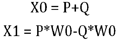
- The data flow corresponding to the function "Rdx-2 Butterfly + windowing" exemplified above may be the following:


- The data flow corresponding to the function "Rdx-2 Butterfly + module" exemplified above may be the following:


- In the first example considered herein, the configuration corresponding to the function "Rdx-2 Butterfly" may involve using two multiplier circuits, two adder-subtractor circuits, no accumulators and no ANLF circuits.
- In the first example considered herein, the configuration corresponding to the function "Rdx-2 Butterfly + windowing" may involve using four multiplier circuits, two adder-subtractor circuits, no accumulators and no ANLF circuits.
- In the first example considered herein, the configuration corresponding to the function "Rdx-2 Butterfly + module" may involve using two multiplier circuits, two adder-subtractor circuits, no accumulators and two ANLF circuits.
- In a second example, configuration of a
computing circuit 20 for performing a scalar product of complex data vectors is described. - A
hardware accelerator circuit 16 may be demanded to compute a scalar product of complex data vectors. For instance, this may be the case of applications involving a filtering operation, such as phased-array radar systems involving a processing stage called beamforming. Beamforming may facilitate a radar system to resolve targets also in the angular (azimuth) dimension, besides the range and radial velocity ones. - In the present second example, the input signals (P, Q, W0, W1, W2, W3, W4) and the output signals (X0, X1) may be complex data type.
- In the present second example, two different scalar vector product operations (e.g., beamforming operations) may be concurrently carried out by a
single processing element 160, e.g., by making use of all the internal hardware resources. - During beamforming operations, the local
configurable coefficient memory 167 may be used to store the phase shifts for the different array antenna elements. - Similarly to the first example, also in the present second example an ANLF circuit may be optionally used if a module is to be computed instead of a complex value.
- Table IV provided at the end of the description exemplifies possible configurations of the
computing circuit 20 for computing concurrently two scalar products of vectors. - Therefore, the data flow corresponding to the function "scalar product of vectors" exemplified above may be the following:

- The data flow corresponding to the function "scalar product of vectors + module" exemplified above may be the following:

- In the second example considered herein, the configuration corresponding to the function "scalar product of vectors" may involve using four multiplier circuits, two adder-subtractor circuits, two accumulators and no ANLF circuits.
- In the second example considered herein, the configuration corresponding to the function "scalar product of vectors + module" may involve using four multiplier circuits, two adder-subtractor circuits, two accumulators and two ANLF circuits.
- In a third example, configuration of a
computing circuit 20 for performing a scalar product of real data vectors is described. - A
hardware accelerator circuit 16 may be demanded to compute a scalar product of real data vectors on large real data structures, e.g., for the computation of a digital filter. For instance, in many applications a real-world (e.g., analog) signal may be subject to filtering after having been digitalized, in order to extract (only) the relevant information. - In the digital domain, a convolution operation between an input signal and a filter impulse response (FIR) may take the form of a scalar product of two real data vectors. One of the two vectors may hold the input data, while the other one may hold the coefficients that define the filtering operation.
- In the present third example, the input signals (P, Q, W0, W1, W2, W3, W4) and the output signals (X0, X1) are real data type.
- In the present third example, two different filtering operations may be concurrently carried out by a
single processing element 160 on the same data set, processing four different input data per clock cycle, e.g., by making use of all the internal hardware resources. - Table V provided at the end of the description exemplifies a possible configuration of the
computing circuit 20 for computing concurrently two filtering operations on real data vectors. - Therefore, the data flow corresponding to the functions exemplified above is the following, where subscript "h" stands for the MSB part, and subscript "l" stands for the LSB part:


- In the third example considered herein, the configuration corresponding to the function "scalar product of real vectors" may involve using four multiplier circuits, two adder-subtractor circuits, two accumulators and no ANLF circuits.
- In a fourth example, configuration of a
computing circuit 20 for computing non-linear functions is described. - Multilayer Perceptron (MLP) is a class of fully-connected feedforward artificial neural networks, which may comprise at least three layers of nodes/neurons. Each neuron, except the ones in the input layer, computes a weighted sum of all the nodes in the previous layer and then applies a non-linear activation function to the result. A
processing element 160 as disclosed herein may handle such non-linear functions, e.g., using the internal ANLF circuits. Typically, neural networks deal with data coming from the real world and use real weights and functions to compute class membership probabilities (the outputs of the last layer). Real data scalar products may thus be the most computationally demanding and most frequently used operations for such kind of artificial networks. -
Figure 5 is a diagram exemplary of a typical structure of aMultilayer Perceptron network 50. - As exemplified in
Figure 5 , aMultiplayer Perceptron network 50 may include: - an
input layer 50a comprising a number N of inputs U1, ..., UN (Ui, i = 1, ..., N), - a
hidden layer 50b comprising a number M of hidden nodes X1, ..., XM (Xk, k = 1, ..., M), and - an
output layer 50c comprising a number P of output nodes Y1, ..., YP (Yj, j = 1, ..., P) . - It will be understood that in one or more embodiments, a Multilayer Perceptron network may comprise more than one hidden
layer 50b. - As exemplified in
Figure 5 , aMultiplayer Perceptron network 50 may include a first set of N*M weights Wi,k between the inputs U1, ..., UN and the hidden nodes X1, ..., XM, and a second set of M*P weights Wk,j between the hidden nodes X1, ..., XM and the output nodes Y1, ..., YP. - The values stored in the inputs Ui, in the hidden nodes Xk and in the output nodes Yj may be computed, for instance, as MAC floating points with single precision.
- The values of the hidden nodes Xk and of the output nodes Yj may be computed according to the following equations:

- In the present fourth example, the trained real weights associated to all the edges of a MLP can be stored inside the local
configurable coefficient memory 167. The real layer inputs may be retrieved from the local data memory of the hardware accelerator circuit 16 (e.g., the local data memory banks M0, ..., MQ-1) and the real layer outputs may be stored into the local data memory of thehardware accelerator circuit 16. - As a result of a MLP model being mapped onto the
hardware accelerator circuit 16, each of theprocessing elements 160 included therein (e.g., a number P of processing elements) may be used to compute the scalar product and the activation function output associated to two different neurons of the same layer, e.g., handling four edges per clock cycle. As a result, all theprocessing elements - Table VI provided at the end of the description exemplifies a possible configuration of the
computing circuit 20 for computing concurrently two activation function outputs associated to two different neurons. - Therefore, the data flow corresponding to the functions exemplified above is the following, where subscript "h" stands for the MSB part, and subscript "l" stands for the LSB part:

- In the fourth example considered herein, the configuration corresponding to the function "MLP computation engine" (which may comprise computing two scalar products of vectors and applying thereto a non-linear activation function) may involve using four multiplier circuits, two adder-subtractor circuits, two accumulators and two ANLF circuits.
- Table VII provided at the end of the description exemplifies non-linear functions which may be implemented in one or more embodiments. Some functions indicated with "Algorithm = NN" may be specifically used in the context of neural networks.
- Therefore, one or more embodiments of a
hardware accelerator circuit 16 comprising at least onecomputing circuit 20 as exemplified herein and/or in the examples above may facilitate implementing a digital signal processing system with one or more of the following advantages: - flexibility (e.g., capability of handling different types of algorithms),
- improved usage of hardware resources,
- improved performance for parallel computation,
- extended connectivity and high bandwidth of each
processing element 160 to the local data memory banks M0, ..., MQ-1 and/or to thesystem memory 12 through a simplelocal interconnect network 162 and internal directmemory access controllers - scalable architecture to support additional algorithms by the integration of different processing elements.
- In one or more embodiments, the
electronic system 1 may be implemented as an integrated circuit in a single silicon chip or die (e.g., as a system-on-chip). Alternatively, theelectronic system 1 may be a distributed system comprising a plurality of integrated circuits interconnected together, e.g., by means of a printed circuit board (PCB). - As exemplified herein, a circuit (e.g., 160) may comprise a set of input terminals configured to receive a respective set of input digital signals carrying input data (e.g., P, Q, W0, W1, W2, W3, W4), a set of output terminals configured to provide a respective set of output digital signals carrying output data (e.g., X0, X1), and computing circuitry (e.g., 20) configured to produce said output data as a function of said input data. The computing circuitry may comprise:
- a set of multiplier circuits (e.g., 30a, 30b, 30c, 30d),
- a set of adder-subtractor circuits (e.g., 32a, 32b),
- a set of accumulator circuits (e.g., 34a, 34b), and
- a configurable interconnect network (e.g., 36a, ..., 36j) configured to selectively couple (e.g., S1, ..., S7) said multiplier circuits, said adder-subtractor circuits, said accumulator circuits, said input terminals and said output terminals in at least two processing configurations.
- As exemplified herein, in a first processing configuration said computing circuitry may be configured to compute said output data according to a first set of functions, and in at least one second processing configuration said computing circuitry may be configured to compute said output data according to a respective second set of functions, said respective second set of functions being different from said first set of functions.
- As exemplified herein, a circuit may comprise respective configurable read direct memory access controllers (e.g., 2000, 2001) coupled to a first subset of said set of input terminals to receive (e.g., 162, 163) a respective first subset of said input digital signals carrying a first subset of input data (e.g., P, Q). The configurable read direct memory access controllers may be configured to control fetching of said first subset of input data from a memory (e.g., Mo, ..., MQ-1).
- As exemplified herein, a circuit may comprise respective configurable write direct memory access controllers (e.g., 2040, 2041) coupled to said set of output terminals for providing said output digital signals carrying output data. The configurable write direct memory access controllers may be configured to control storage of said output data into said memory.
- As exemplified herein, a circuit may comprise respective input buffer registers (e.g., 2020, 2021) coupled to said configurable read direct memory access controllers and respective output buffer registers (e.g., 2060, 2061) coupled to said configurable write direct memory access controllers.
- As exemplified herein, a circuit may comprise a ROM address generator circuit (e.g., 208) configured to control fetching of a second subset of input data (e.g., W0) from at least one read-only memory (e.g., 164, 165) via a second subset of said input digital signals, and/or a memory address generator circuit (e.g., 210) configured to control fetching of a third subset of input data (e.g., W1, W2, W3, W4) from at least one configurable memory (e.g., 166, 167) via a third subset of said input digital signals.
- As exemplified herein, in a circuit according to embodiments said set of multiplier circuits may comprise a first multiplier circuit (e.g., 30a), a second multiplier circuit (e.g., 30b), a third multiplier circuit (e.g., 30c) and a fourth multiplier circuit (e.g., 30d). The set of adder-subtractor circuits may comprise a first adder-subtractor circuit (e.g., 32a) and a second adder-subtractor circuit (32b). The set of accumulator circuits may comprise a first accumulator circuit (e.g., 34a) and a second accumulator circuit (e.g., 34b).
- As exemplified herein, the first multiplier circuit may receive as a first operand a first input signal (e.g., W1) of said set of input digital signals, and may receive as a second operand a second input signal (e.g., P) of said set of input digital signals. The second multiplier circuit may receive as a first operand a third input signal (e.g., Q) of said set of input digital signals, and may receive as a second operand a signal selectable out of a fourth input signal (e.g., W2) and a fifth input signal (e.g., W4) of said set of input digital signals. The third multiplier circuit may receive as a first operand a signal selectable out of an output signal from said first multiplier circuit and said second input signal, and may receive as a second operand a signal selectable out of a sixth input signal (e.g., W3), a seventh input signal (e.g., W0) and said fifth input signal. The fourth multiplier circuit may receive as a first operand a signal selectable out of an output signal from said second multiplier and said third input signal, and may receive as a second operand a signal selectable out of said fifth input signal and said seventh input signal. The first adder-subtractor circuit may receive as a first operand a signal selectable out of said output signal from said first multiplier circuit, said second input signal and said output signal from said third multiplier circuit, and may receive as a second operand a signal selectable out of said third input signal, said output signal from said second multiplier circuit and a null signal. The second adder-subtractor circuit may receive as a first operand a signal selectable out of said output signal from said third multiplier circuit and said output signal from said fourth multiplier circuit, and may receive as a second operand a signal selectable out of said output signal from said fourth multiplier circuit, said output signal from said second multiplier circuit and a null signal. The first accumulator circuit may receive as input an output signal from said first adder-subtractor circuit, and the second accumulator circuit may receive as input an output signal from said second adder-subtractor circuit. The first accumulator circuit maybe selectively activatable (e.g., EN) to provide a first output signal (e.g., X0) and said second accumulator circuit may be selectively activatable to provide a second output signal (e.g., X1).
- As exemplified herein, said computing circuitry may comprise a set of circuits configured to compute non-linear functions (e.g., 40a, 40b).
- As exemplified herein, said set of circuits configured to compute non-linear functions may comprise a first circuit configured to compute non-linear functions (e.g., 40a) and a second circuit configured to compute non-linear functions (e.g., 40b). The first circuit configured to compute non-linear functions may receive as input an output signal from said first accumulator circuit. The second circuit configured to compute non-linear functions may receive as input an output signal from said second accumulator circuit. The first output signal may be selectable (e.g., 36k) between the output signal from the first accumulator circuit and the output signal from the first circuit configured to compute non-linear functions, and the second output signal may be selectable (e.g., 36m) between the output signal from the second accumulator circuit and the output signal from the second circuit configured to compute non-linear functions.
- As exemplified herein, a device (e.g., 16) may comprise a set of circuits according to one or more embodiments, a set of data memory banks (e.g., Mo, ..., MQ-1) and a control unit (e.g., 161). The circuits may be configurable (e.g., 161, 168) to read data from and write data into said data memory banks via an interconnect network (e.g., 162, 163) as a function of configuration data stored in said control unit.
- As exemplified herein, said data memory banks may comprise buffering registers, preferably double buffering registers.
- As exemplified herein, a system (e.g., 1) may comprise a device according to one or more embodiments and a processing unit (e.g., 10) coupled to the device via a system interconnect (e.g., 18). The circuits in the set of circuits of the device may be configurable in at least two processing configurations as a function of a control signal received from the processing unit.
- As exemplified herein, a method of operating a circuit according to one or more embodiments, a device according to one or more embodiments, or a system according to one or more embodiments may comprise partitioning the operation time of said computing circuitry in at least first and second operation intervals, wherein said computing circuitry is operated in said first processing configuration and said at least one second processing configuration, respectively.
- Without prejudice to the underlying principles, the details and embodiments may vary, even significantly, with respect to what has been described by way of example only, without departing from the extent of protection.
- The extent of protection is defined by the annexed claims.
Table I-1 SP0 SP1 ... SPP-1 SPP SPP+1 MP0 X MP1 X ... ... MPP-1 X MPP X Table 1-2 SP0 SP1 ... SPP-1 SPP SPP+1 MP0 X X MP1 X X ... ... ... MPP-1 X X MPP X Table 1-3 SP0 SP1 ... SPP-1 SPP SPP+1 MP0 X X MP1 X X ... ... ... MPP-1 X X MPP X (X) (X) (X) X Table II S 8 Output functioning Inputs Outre (real) Outimg (imaginary) 0 Outre =In0re ∗In1re Outimg=In0img ∗In1img In0: 2 real data In1: 2 real data 1 Outre=Re(In0∗In 1) Outimg=Img(In0∗In1) In0: 1 complex data In1: 1 complex data Table III Function Configuration S 0 S 1 S 2 S 3 S 4 S 5 S 6 S 7 S 8 S 9E N G 0 G 1Rdx-2 Butt. 1 0 - 1 0 0 0 1 1 0 0 1 1 Rdx-2 Butt. + Windowin g 0 1 0 1 0 0 1 1 1 0 0 1 1 Rdx-2 Butt. + Module 1 0 - 1 0 0 0 1 1 1 0 1 1 Table IV Function Configuration S 0 S 1 S 2 S 3 S 4 S 5 S 6 S 7 S 8 S 9 E N G 0 G 1 2x scalar product of vectors (complex ) 0 0 0 0 0 0 1 1 1 0 1 1 1 2x scalar product of vectors (complex ) + Module 0 0 0 0 0 0 1 1 1 1 1 1 1 Table V Function Configuration S0 S1 S2 S3 S4 S5 S6 S7 S8 S9 EN G0 G1 2x scalar product of vectors (real) 0 0 0 0 0 0 1 1 0 0 1 1 1 Table VI Function Configuration S0 S1 S2 S3 S4 S5 S6 S7 S8 S9 EN G0 G1 MLP computation engine 0 0 0 0 0 0 1 1 0 1 1 1 1 Table VII Name Function Algorithm Sigmoid (σ) Logistic function 
NN tanh hyperbolic tangent 
NN ReLU Rectified Linear Unit 
NN Softmax 
NN Leaky_ReLU 
NN SELU Scaled ELU 
NN Hard sigmoid 
NN ELU Exponential LU 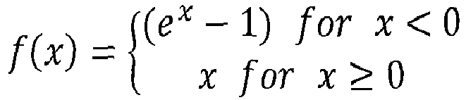
NN Log (x) f(x) = log (x) f or x ≥ 0 Sin (x) f(x) = sin (x) Cos(x) f(x) = cos (x) Abs (x) 
Sqrt (x) 
Module (z = re + im) Phase (z = re + im) 
Claims (11)
- A circuit (160) comprising:a set of input terminals configured to receive a set of respective input digital signals carrying input data (P, Q, W0, W1, W2, W3, W4),a set of output terminals configured to provide a set of respective output digital signals carrying output data (X0, X1), andcomputing circuitry (20) configured to produce said output data as a function of said input data, wherein the computing circuitry (20) comprises:a set of multiplier circuits (30a, 30b, 30c, 30d),a set of adder-subtractor circuits (32a, 32b),a set of accumulator circuits (34a, 34b), anda configurable interconnect network (36a, ..., 36j) configured to selectively couple (S1, ..., S7) said multiplier circuits (30a, 30b, 30c, 30d), said adder-subtractor circuits (32a, 32b), said accumulator circuits (34a, 34b), said input terminals and said output terminals in at least two processing configurations,wherein:in a first processing configuration, said computing circuitry (20) is configured to compute said output data (X0, X1) according to a first set of functions, andin at least one second processing configuration, said computing circuitry (20) is configured to compute said output data (X0, X1) according to a respective second set of functions, said respective second set of functions being different from said first set of functions.
- The circuit (160) of claim 1, comprising:respective configurable read direct memory access controllers (2000, 2001) coupled to a first subset of said set of input terminals to receive (162, 163) a respective first subset of said input digital signals carrying a first subset of input data (P, Q), wherein said configurable read direct memory access controllers (2000, 2001) are configured to control fetching of said first subset of input data (P, Q) from a memory (M0, ..., MQ-1) , andrespective configurable write direct memory access controllers (2040, 2041) coupled to said set of output terminals for providing (162, 163) said output digital signals carrying output data (X0, X1), wherein said configurable write direct memory access controllers (2040, 2041) are configured to control storage of said output data (X0, X1) into said memory (M0, ..., MQ-1).
- The circuit (160) of claim 2, comprising respective input buffer registers (2020, 2021) coupled to said configurable read direct memory access controllers (2000, 2001) and respective output buffer registers (2060, 2061) coupled to said configurable write direct memory access controllers (2040, 2041) .
- The circuit (160) of any of the previous claims, comprising:a ROM address generator circuit (208) configured to control fetching of a second subset of input data (W0) from at least one read-only memory (164, 165) via a second subset of said input digital signals, and/ora memory address generator circuit (210) configured to control fetching of a third subset of input data (W1, W2, W3, W4) from at least one local configurable memory (166, 167) via a third subset of said input digital signals.
- The circuit (160) of any of the previous claims, wherein said set of multiplier circuits comprises a first multiplier circuit (30a), a second multiplier circuit (30b), a third multiplier circuit (30c) and a fourth multiplier circuit (30d), said set of adder-subtractor circuits (32a, 32b) comprises a first adder-subtractor circuit (32a) and a second adder-subtractor circuit (32b), and said set of accumulator circuits comprises a first accumulator circuit (34a) and a second accumulator circuit (34b), and wherein:said first multiplier circuit (30a) receives as a first operand a first input signal (W1) of said set of input digital signals, and receives as a second operand a second input signal (P) of said set of input digital signals,said second multiplier circuit (30b) receives as a first operand a third input signal (Q) of said set of input digital signals, and receives as a second operand a signal selectable out of a fourth input signal (W2) and a fifth input signal (W4) of said set of input digital signals,said third multiplier circuit (30c) receives as a first operand a signal selectable out of an output signal from said first multiplier circuit (30a) and said second input signal (P), and receives as a second operand a signal selectable out of a sixth input signal (W3), a seventh input signal (W0) and said fifth input signal (W4),said fourth multiplier circuit (30d) receives as a first operand a signal selectable out of an output signal from said second multiplier (30b) and said third input signal (Q), and receives as a second operand a signal selectable out of said fifth input signal (W4) and said seventh input signal (W0),said first adder-subtractor circuit (32a) receives as a first operand a signal selectable out of said output signal from said first multiplier circuit (30a), said second input signal (P) and said output signal from said third multiplier circuit (30c), and receives as a second operand a signal selectable out of said third input signal (Q), said output signal from said second multiplier circuit (30b) and a null signal,said second adder-subtractor circuit (32b) receives as a first operand a signal selectable out of said output signal from said third multiplier circuit (30c) and said output signal from said fourth multiplier circuit (30d), and receives as a second operand a signal selectable out of said output signal from said fourth multiplier circuit (30d), said output signal from said second multiplier circuit (30b) and a null signal,said first accumulator circuit (34a) receives as input an output signal from said first adder-subtractor circuit (32a),said second accumulator circuit (34b) receives as input an output signal from said second adder-subtractor circuit (32b), andsaid first accumulator circuit (34a) is selectively activatable (EN) to provide a first output signal (X0) and said second accumulator circuit (34b) is selectively activatable (EN) to provide a second output signal (X1).
- The circuit (160) of claim 5, wherein said computing circuitry (20) comprises a set of circuits configured to compute non-linear functions (40a, 40b).
- The circuit (160) of claim 6, wherein said set of circuits configured to compute non-linear functions (40a, 40b) comprises a first circuit configured to compute non-linear functions (40a) and a second circuit configured to compute non-linear functions (40b), and wherein:said first circuit configured to compute non-linear functions (40a) receives as input an output signal from said first accumulator circuit (34a),said second circuit configured to compute non-linear functions (40b) receives as input an output signal from said second accumulator circuit (34b),said first output signal (X0) is selectable (36k) between the output signal from the first accumulator circuit (34a) and the output signal from the first circuit configured to compute non-linear functions (40a), andsaid second output signal (X1) is selectable (36m) between the output signal from the second accumulator circuit (34b) and the output signal from the second circuit configured to compute non-linear functions (40b).
- A device (16) comprising a set of circuits (160) according to any of the previous claims, a set of data memory banks (M0, ..., MQ-1) and a control unit (161), wherein the circuits (160) are configurable (161, 168) to read data from and write data into said data memory banks (M0, ..., MQ-1) via an interconnect network (162, 163) as a function of configuration data stored in said control unit (161).
- The device (16) of claim 8, wherein said data memory banks (M0, ..., MQ-1) comprise buffering registers, preferably double buffering registers.
- A system (1) comprising a device (16) according to claim 8 or claim 9 and a processing unit (10) coupled to the device (16) via a system interconnect (18), wherein the circuits in the set of circuits (160) of the device (16) are configurable in at least two processing configurations as a function of a control signal received from the processing unit (10).
- A method of operating a circuit (160) according to any of claims 1 to 7, a device (16) according to claim 8 or claim 9, or a system (1) according to claim 10, the method comprising partitioning the operation time of said computing circuitry (20) in at least first and second operation intervals, wherein said computing circuitry (20) is operated in said first processing configuration and said at least one second processing configuration, respectively.
Applications Claiming Priority (1)
| Application Number | Priority Date | Filing Date | Title |
|---|---|---|---|
| IT102020000009358A IT202000009358A1 (en) | 2020-04-29 | 2020-04-29 | CORRESPONDING CIRCUIT, DEVICE, SYSTEM AND PROCEDURE |
Publications (2)
| Publication Number | Publication Date |
|---|---|
| EP3905036A1 true EP3905036A1 (en) | 2021-11-03 |
| EP3905036B1 EP3905036B1 (en) | 2024-08-28 |
Family
ID=71452679
Family Applications (1)
| Application Number | Title | Priority Date | Filing Date |
|---|---|---|---|
| EP21168368.5A Active EP3905036B1 (en) | 2020-04-29 | 2021-04-14 | Reconfigurable circuit, corresponding device, system and method |
Country Status (3)
| Country | Link |
|---|---|
| US (1) | US11354257B2 (en) |
| EP (1) | EP3905036B1 (en) |
| IT (1) | IT202000009358A1 (en) |
Families Citing this family (5)
| Publication number | Priority date | Publication date | Assignee | Title |
|---|---|---|---|---|
| US20210350221A1 (en) * | 2020-05-05 | 2021-11-11 | Silicon Laboratories Inc. | Neural Network Inference and Training Using A Universal Coordinate Rotation Digital Computer |
| US12141683B2 (en) * | 2021-04-30 | 2024-11-12 | Intel Corporation | Performance scaling for dataflow deep neural network hardware accelerators |
| US12394009B2 (en) * | 2021-05-28 | 2025-08-19 | MemComputing, Inc. | Memory graphics processing unit |
| CN117539426A (en) * | 2022-08-02 | 2024-02-09 | 阿里巴巴(中国)有限公司 | Multiplication unit, digital domain conversion circuit, and privacy calculation device |
| US12360932B2 (en) * | 2023-12-06 | 2025-07-15 | Cypress Semiconductor Corporation | Coordinate rotation digital computer using direct memory access engines |
Citations (2)
| Publication number | Priority date | Publication date | Assignee | Title |
|---|---|---|---|---|
| US6041140A (en) * | 1994-10-04 | 2000-03-21 | Synthonics, Incorporated | Apparatus for interactive image correlation for three dimensional image production |
| US20070283128A1 (en) * | 2006-06-06 | 2007-12-06 | Matsushita Electric Industrial Co., Ltd. | Asymmetric multiprocessor |
Family Cites Families (8)
| Publication number | Priority date | Publication date | Assignee | Title |
|---|---|---|---|---|
| DE19651075A1 (en) * | 1996-12-09 | 1998-06-10 | Pact Inf Tech Gmbh | Unit for processing numerical and logical operations, for use in processors (CPU's), multi-computer systems, data flow processors (DFP's), digital signal processors (DSP's) or the like |
| US7933295B2 (en) * | 1999-04-13 | 2011-04-26 | Broadcom Corporation | Cable modem with voice processing capability |
| US20050275427A1 (en) * | 2004-06-10 | 2005-12-15 | Man Wang | Field programmable gate array logic unit and its cluster |
| US7164290B2 (en) * | 2004-06-10 | 2007-01-16 | Klp International, Ltd. | Field programmable gate array logic unit and its cluster |
| US8938799B2 (en) * | 2004-06-28 | 2015-01-20 | Jen-Wei Kuo | Security protection apparatus and method for endpoint computing systems |
| DE102004056738B3 (en) * | 2004-11-24 | 2006-05-18 | Infineon Technologies Ag | Programmable logic cell for a programmable logic array, arithmetic unit and digital circuitry |
| US8457653B2 (en) * | 2011-02-25 | 2013-06-04 | Nokia Corporation | Method and apparatus for pre-fetching location-based data while maintaining user privacy |
| US9432624B2 (en) * | 2014-01-03 | 2016-08-30 | Clearone Communications Hong Kong Ltd. | Method for improving an MCU's performance using common properties of the H.264 codec standard |
-
2020
- 2020-04-29 IT IT102020000009358A patent/IT202000009358A1/en unknown
-
2021
- 2021-04-07 US US17/224,772 patent/US11354257B2/en active Active
- 2021-04-14 EP EP21168368.5A patent/EP3905036B1/en active Active
Patent Citations (2)
| Publication number | Priority date | Publication date | Assignee | Title |
|---|---|---|---|---|
| US6041140A (en) * | 1994-10-04 | 2000-03-21 | Synthonics, Incorporated | Apparatus for interactive image correlation for three dimensional image production |
| US20070283128A1 (en) * | 2006-06-06 | 2007-12-06 | Matsushita Electric Industrial Co., Ltd. | Asymmetric multiprocessor |
Non-Patent Citations (1)
| Title |
|---|
| STRUHARIK RASTISLAV ET AL: "CoNNA - Compressed CNN Hardware Accelerator", 2018 21ST EUROMICRO CONFERENCE ON DIGITAL SYSTEM DESIGN (DSD), IEEE, 29 August 2018 (2018-08-29), pages 365 - 372, XP033420220, DOI: 10.1109/DSD.2018.00070 * |
Also Published As
| Publication number | Publication date |
|---|---|
| EP3905036B1 (en) | 2024-08-28 |
| US20210342277A1 (en) | 2021-11-04 |
| US11354257B2 (en) | 2022-06-07 |
| IT202000009358A1 (en) | 2021-10-29 |
Similar Documents
| Publication | Publication Date | Title |
|---|---|---|
| US11354257B2 (en) | Circuit, corresponding device, system and method | |
| CN107871163B (en) | Operation device and method for convolutional neural network | |
| US4791590A (en) | High performance signal processor | |
| US7979673B2 (en) | Method and apparatus for matrix decompositions in programmable logic devices | |
| TWI782328B (en) | Processor for neural network operation | |
| CN113568851B (en) | Method for accessing memory and corresponding circuit | |
| Fan et al. | DT-CGRA: Dual-track coarse-grained reconfigurable architecture for stream applications | |
| US7558943B2 (en) | Processing unit for broadcast parallel processing | |
| US11620077B2 (en) | Method of accessing a memory, and corresponding circuit | |
| US20200082242A1 (en) | Convolutional neural network using adaptive 3d array | |
| US20210255861A1 (en) | Arithmetic logic unit | |
| Sung | Memory-efficient and high-speed split-radix FFT/IFFT processor based on pipelined CORDIC rotations | |
| Wang et al. | Design of pipelined FFT processor based on FPGA | |
| Zhou et al. | Double precision hybrid-mode floating-point FPGA CORDIC co-processor | |
| US7194497B2 (en) | Hardware-based accelerator for time-domain scientific computing | |
| US6615227B2 (en) | Circuit and method for computing a fast fourier transform | |
| US20160314096A1 (en) | Fft device and method for performing a fast fourier transform | |
| CN113568864B (en) | Circuit, corresponding device, system and method | |
| Takala et al. | Butterfly unit supporting radix-4 and radix-2 FFT | |
| Kallapu et al. | DRRA-based reconfigurable architecture for mixed-radix FFT | |
| EP1538533A2 (en) | Improved FFT/IFFT processor | |
| Jadhav et al. | Autorare: An automated tool for generating fpga-based multi-memory hardware accelerators for compute-intensive applications | |
| JP7447088B2 (en) | Vectorized peak detection for signal processing | |
| Inguva et al. | FPGA based Implementation of Low power CORDIC architecture | |
| Covert | A 32 point monolithic FFT processor chip |
Legal Events
| Date | Code | Title | Description |
|---|---|---|---|
| PUAI | Public reference made under article 153(3) epc to a published international application that has entered the european phase |
Free format text: ORIGINAL CODE: 0009012 |
|
| STAA | Information on the status of an ep patent application or granted ep patent |
Free format text: STATUS: THE APPLICATION HAS BEEN PUBLISHED |
|
| AK | Designated contracting states |
Kind code of ref document: A1 Designated state(s): AL AT BE BG CH CY CZ DE DK EE ES FI FR GB GR HR HU IE IS IT LI LT LU LV MC MK MT NL NO PL PT RO RS SE SI SK SM TR |
|
| B565 | Issuance of search results under rule 164(2) epc |
Effective date: 20210511 |
|
| STAA | Information on the status of an ep patent application or granted ep patent |
Free format text: STATUS: REQUEST FOR EXAMINATION WAS MADE |
|
| 17P | Request for examination filed |
Effective date: 20220422 |
|
| RBV | Designated contracting states (corrected) |
Designated state(s): AL AT BE BG CH CY CZ DE DK EE ES FI FR GB GR HR HU IE IS IT LI LT LU LV MC MK MT NL NO PL PT RO RS SE SI SK SM TR |
|
| GRAP | Despatch of communication of intention to grant a patent |
Free format text: ORIGINAL CODE: EPIDOSNIGR1 |
|
| STAA | Information on the status of an ep patent application or granted ep patent |
Free format text: STATUS: GRANT OF PATENT IS INTENDED |
|
| INTG | Intention to grant announced |
Effective date: 20240418 |
|
| RIN1 | Information on inventor provided before grant (corrected) |
Inventor name: RE FIORENTIN, LORENZO Inventor name: BORGONOVO, GIAMPIERO |
|
| GRAS | Grant fee paid |
Free format text: ORIGINAL CODE: EPIDOSNIGR3 |
|
| GRAA | (expected) grant |
Free format text: ORIGINAL CODE: 0009210 |
|
| STAA | Information on the status of an ep patent application or granted ep patent |
Free format text: STATUS: THE PATENT HAS BEEN GRANTED |
|
| AK | Designated contracting states |
Kind code of ref document: B1 Designated state(s): AL AT BE BG CH CY CZ DE DK EE ES FI FR GB GR HR HU IE IS IT LI LT LU LV MC MK MT NL NO PL PT RO RS SE SI SK SM TR |
|
| REG | Reference to a national code |
Ref country code: CH Ref legal event code: EP |
|
| REG | Reference to a national code |
Ref country code: DE Ref legal event code: R096 Ref document number: 602021017749 Country of ref document: DE |
|
| REG | Reference to a national code |
Ref country code: IE Ref legal event code: FG4D |
|
| REG | Reference to a national code |
Ref country code: LT Ref legal event code: MG9D |
|
| PG25 | Lapsed in a contracting state [announced via postgrant information from national office to epo] |
Ref country code: NO Free format text: LAPSE BECAUSE OF FAILURE TO SUBMIT A TRANSLATION OF THE DESCRIPTION OR TO PAY THE FEE WITHIN THE PRESCRIBED TIME-LIMIT Effective date: 20241128 |
|
| REG | Reference to a national code |
Ref country code: AT Ref legal event code: MK05 Ref document number: 1718702 Country of ref document: AT Kind code of ref document: T Effective date: 20240828 |
|
| PG25 | Lapsed in a contracting state [announced via postgrant information from national office to epo] |
Ref country code: NL Free format text: LAPSE BECAUSE OF FAILURE TO SUBMIT A TRANSLATION OF THE DESCRIPTION OR TO PAY THE FEE WITHIN THE PRESCRIBED TIME-LIMIT Effective date: 20240828 Ref country code: PT Free format text: LAPSE BECAUSE OF FAILURE TO SUBMIT A TRANSLATION OF THE DESCRIPTION OR TO PAY THE FEE WITHIN THE PRESCRIBED TIME-LIMIT Effective date: 20241230 Ref country code: GR Free format text: LAPSE BECAUSE OF FAILURE TO SUBMIT A TRANSLATION OF THE DESCRIPTION OR TO PAY THE FEE WITHIN THE PRESCRIBED TIME-LIMIT Effective date: 20241129 Ref country code: PL Free format text: LAPSE BECAUSE OF FAILURE TO SUBMIT A TRANSLATION OF THE DESCRIPTION OR TO PAY THE FEE WITHIN THE PRESCRIBED TIME-LIMIT Effective date: 20240828 Ref country code: FI Free format text: LAPSE BECAUSE OF FAILURE TO SUBMIT A TRANSLATION OF THE DESCRIPTION OR TO PAY THE FEE WITHIN THE PRESCRIBED TIME-LIMIT Effective date: 20240828 |
|
| PG25 | Lapsed in a contracting state [announced via postgrant information from national office to epo] |
Ref country code: BG Free format text: LAPSE BECAUSE OF FAILURE TO SUBMIT A TRANSLATION OF THE DESCRIPTION OR TO PAY THE FEE WITHIN THE PRESCRIBED TIME-LIMIT Effective date: 20240828 |
|
| PG25 | Lapsed in a contracting state [announced via postgrant information from national office to epo] |
Ref country code: LV Free format text: LAPSE BECAUSE OF FAILURE TO SUBMIT A TRANSLATION OF THE DESCRIPTION OR TO PAY THE FEE WITHIN THE PRESCRIBED TIME-LIMIT Effective date: 20240828 |
|
| REG | Reference to a national code |
Ref country code: NL Ref legal event code: MP Effective date: 20240828 |
|
| PG25 | Lapsed in a contracting state [announced via postgrant information from national office to epo] |
Ref country code: AT Free format text: LAPSE BECAUSE OF FAILURE TO SUBMIT A TRANSLATION OF THE DESCRIPTION OR TO PAY THE FEE WITHIN THE PRESCRIBED TIME-LIMIT Effective date: 20240828 Ref country code: IS Free format text: LAPSE BECAUSE OF FAILURE TO SUBMIT A TRANSLATION OF THE DESCRIPTION OR TO PAY THE FEE WITHIN THE PRESCRIBED TIME-LIMIT Effective date: 20241228 |
|
| PG25 | Lapsed in a contracting state [announced via postgrant information from national office to epo] |
Ref country code: HR Free format text: LAPSE BECAUSE OF FAILURE TO SUBMIT A TRANSLATION OF THE DESCRIPTION OR TO PAY THE FEE WITHIN THE PRESCRIBED TIME-LIMIT Effective date: 20240828 |
|
| PG25 | Lapsed in a contracting state [announced via postgrant information from national office to epo] |
Ref country code: RS Free format text: LAPSE BECAUSE OF FAILURE TO SUBMIT A TRANSLATION OF THE DESCRIPTION OR TO PAY THE FEE WITHIN THE PRESCRIBED TIME-LIMIT Effective date: 20241128 Ref country code: ES Free format text: LAPSE BECAUSE OF FAILURE TO SUBMIT A TRANSLATION OF THE DESCRIPTION OR TO PAY THE FEE WITHIN THE PRESCRIBED TIME-LIMIT Effective date: 20240828 |
|
| PG25 | Lapsed in a contracting state [announced via postgrant information from national office to epo] |
Ref country code: RS Free format text: LAPSE BECAUSE OF FAILURE TO SUBMIT A TRANSLATION OF THE DESCRIPTION OR TO PAY THE FEE WITHIN THE PRESCRIBED TIME-LIMIT Effective date: 20241128 Ref country code: PT Free format text: LAPSE BECAUSE OF FAILURE TO SUBMIT A TRANSLATION OF THE DESCRIPTION OR TO PAY THE FEE WITHIN THE PRESCRIBED TIME-LIMIT Effective date: 20241230 Ref country code: PL Free format text: LAPSE BECAUSE OF FAILURE TO SUBMIT A TRANSLATION OF THE DESCRIPTION OR TO PAY THE FEE WITHIN THE PRESCRIBED TIME-LIMIT Effective date: 20240828 Ref country code: NO Free format text: LAPSE BECAUSE OF FAILURE TO SUBMIT A TRANSLATION OF THE DESCRIPTION OR TO PAY THE FEE WITHIN THE PRESCRIBED TIME-LIMIT Effective date: 20241128 Ref country code: NL Free format text: LAPSE BECAUSE OF FAILURE TO SUBMIT A TRANSLATION OF THE DESCRIPTION OR TO PAY THE FEE WITHIN THE PRESCRIBED TIME-LIMIT Effective date: 20240828 Ref country code: LV Free format text: LAPSE BECAUSE OF FAILURE TO SUBMIT A TRANSLATION OF THE DESCRIPTION OR TO PAY THE FEE WITHIN THE PRESCRIBED TIME-LIMIT Effective date: 20240828 Ref country code: IS Free format text: LAPSE BECAUSE OF FAILURE TO SUBMIT A TRANSLATION OF THE DESCRIPTION OR TO PAY THE FEE WITHIN THE PRESCRIBED TIME-LIMIT Effective date: 20241228 Ref country code: HR Free format text: LAPSE BECAUSE OF FAILURE TO SUBMIT A TRANSLATION OF THE DESCRIPTION OR TO PAY THE FEE WITHIN THE PRESCRIBED TIME-LIMIT Effective date: 20240828 Ref country code: GR Free format text: LAPSE BECAUSE OF FAILURE TO SUBMIT A TRANSLATION OF THE DESCRIPTION OR TO PAY THE FEE WITHIN THE PRESCRIBED TIME-LIMIT Effective date: 20241129 Ref country code: FI Free format text: LAPSE BECAUSE OF FAILURE TO SUBMIT A TRANSLATION OF THE DESCRIPTION OR TO PAY THE FEE WITHIN THE PRESCRIBED TIME-LIMIT Effective date: 20240828 Ref country code: ES Free format text: LAPSE BECAUSE OF FAILURE TO SUBMIT A TRANSLATION OF THE DESCRIPTION OR TO PAY THE FEE WITHIN THE PRESCRIBED TIME-LIMIT Effective date: 20240828 Ref country code: BG Free format text: LAPSE BECAUSE OF FAILURE TO SUBMIT A TRANSLATION OF THE DESCRIPTION OR TO PAY THE FEE WITHIN THE PRESCRIBED TIME-LIMIT Effective date: 20240828 Ref country code: AT Free format text: LAPSE BECAUSE OF FAILURE TO SUBMIT A TRANSLATION OF THE DESCRIPTION OR TO PAY THE FEE WITHIN THE PRESCRIBED TIME-LIMIT Effective date: 20240828 |
|
| PG25 | Lapsed in a contracting state [announced via postgrant information from national office to epo] |
Ref country code: RO Free format text: LAPSE BECAUSE OF FAILURE TO SUBMIT A TRANSLATION OF THE DESCRIPTION OR TO PAY THE FEE WITHIN THE PRESCRIBED TIME-LIMIT Effective date: 20240828 Ref country code: SM Free format text: LAPSE BECAUSE OF FAILURE TO SUBMIT A TRANSLATION OF THE DESCRIPTION OR TO PAY THE FEE WITHIN THE PRESCRIBED TIME-LIMIT Effective date: 20240828 Ref country code: DK Free format text: LAPSE BECAUSE OF FAILURE TO SUBMIT A TRANSLATION OF THE DESCRIPTION OR TO PAY THE FEE WITHIN THE PRESCRIBED TIME-LIMIT Effective date: 20240828 |
|
| PG25 | Lapsed in a contracting state [announced via postgrant information from national office to epo] |
Ref country code: EE Free format text: LAPSE BECAUSE OF FAILURE TO SUBMIT A TRANSLATION OF THE DESCRIPTION OR TO PAY THE FEE WITHIN THE PRESCRIBED TIME-LIMIT Effective date: 20240828 |
|
| PG25 | Lapsed in a contracting state [announced via postgrant information from national office to epo] |
Ref country code: CZ Free format text: LAPSE BECAUSE OF FAILURE TO SUBMIT A TRANSLATION OF THE DESCRIPTION OR TO PAY THE FEE WITHIN THE PRESCRIBED TIME-LIMIT Effective date: 20240828 |
|
| PG25 | Lapsed in a contracting state [announced via postgrant information from national office to epo] |
Ref country code: IT Free format text: LAPSE BECAUSE OF FAILURE TO SUBMIT A TRANSLATION OF THE DESCRIPTION OR TO PAY THE FEE WITHIN THE PRESCRIBED TIME-LIMIT Effective date: 20240828 Ref country code: SK Free format text: LAPSE BECAUSE OF FAILURE TO SUBMIT A TRANSLATION OF THE DESCRIPTION OR TO PAY THE FEE WITHIN THE PRESCRIBED TIME-LIMIT Effective date: 20240828 |
|
| REG | Reference to a national code |
Ref country code: DE Ref legal event code: R097 Ref document number: 602021017749 Country of ref document: DE |
|
| PLBE | No opposition filed within time limit |
Free format text: ORIGINAL CODE: 0009261 |
|
| STAA | Information on the status of an ep patent application or granted ep patent |
Free format text: STATUS: NO OPPOSITION FILED WITHIN TIME LIMIT |
|
| PGFP | Annual fee paid to national office [announced via postgrant information from national office to epo] |
Ref country code: DE Payment date: 20250319 Year of fee payment: 5 |
|
| 26N | No opposition filed |
Effective date: 20250530 |
|
| PG25 | Lapsed in a contracting state [announced via postgrant information from national office to epo] |
Ref country code: SE Free format text: LAPSE BECAUSE OF FAILURE TO SUBMIT A TRANSLATION OF THE DESCRIPTION OR TO PAY THE FEE WITHIN THE PRESCRIBED TIME-LIMIT Effective date: 20240828 |
|
| REG | Reference to a national code |
Ref country code: CH Ref legal event code: H13 Free format text: ST27 STATUS EVENT CODE: U-0-0-H10-H13 (AS PROVIDED BY THE NATIONAL OFFICE) Effective date: 20251125 |
|
| PG25 | Lapsed in a contracting state [announced via postgrant information from national office to epo] |
Ref country code: LU Free format text: LAPSE BECAUSE OF NON-PAYMENT OF DUE FEES Effective date: 20250414 |
|
| PG25 | Lapsed in a contracting state [announced via postgrant information from national office to epo] |
Ref country code: MC Free format text: LAPSE BECAUSE OF FAILURE TO SUBMIT A TRANSLATION OF THE DESCRIPTION OR TO PAY THE FEE WITHIN THE PRESCRIBED TIME-LIMIT Effective date: 20240828 |
|
| GBPC | Gb: european patent ceased through non-payment of renewal fee |
Effective date: 20250414 |
|
| REG | Reference to a national code |
Ref country code: BE Ref legal event code: MM Effective date: 20250430 |
|
| PG25 | Lapsed in a contracting state [announced via postgrant information from national office to epo] |
Ref country code: GB Free format text: LAPSE BECAUSE OF NON-PAYMENT OF DUE FEES Effective date: 20250414 |
|
| PG25 | Lapsed in a contracting state [announced via postgrant information from national office to epo] |
Ref country code: FR Free format text: LAPSE BECAUSE OF NON-PAYMENT OF DUE FEES Effective date: 20250430 |
|
| PG25 | Lapsed in a contracting state [announced via postgrant information from national office to epo] |
Ref country code: BE Free format text: LAPSE BECAUSE OF NON-PAYMENT OF DUE FEES Effective date: 20250430 |
|
| PG25 | Lapsed in a contracting state [announced via postgrant information from national office to epo] |
Ref country code: CH Free format text: LAPSE BECAUSE OF NON-PAYMENT OF DUE FEES Effective date: 20250430 |
|
| PG25 | Lapsed in a contracting state [announced via postgrant information from national office to epo] |
Ref country code: IE Free format text: LAPSE BECAUSE OF NON-PAYMENT OF DUE FEES Effective date: 20250414 |