EP3904865A1 - Image processing device, image processing method, and image processing program - Google Patents
Image processing device, image processing method, and image processing program Download PDFInfo
- Publication number
- EP3904865A1 EP3904865A1 EP19901921.7A EP19901921A EP3904865A1 EP 3904865 A1 EP3904865 A1 EP 3904865A1 EP 19901921 A EP19901921 A EP 19901921A EP 3904865 A1 EP3904865 A1 EP 3904865A1
- Authority
- EP
- European Patent Office
- Prior art keywords
- image
- defect
- defect image
- background
- image processing
- Prior art date
- Legal status (The legal status is an assumption and is not a legal conclusion. Google has not performed a legal analysis and makes no representation as to the accuracy of the status listed.)
- Granted
Links
Images


Classifications
-
- G—PHYSICS
- G06—COMPUTING OR CALCULATING; COUNTING
- G06T—IMAGE DATA PROCESSING OR GENERATION, IN GENERAL
- G06T7/00—Image analysis
- G06T7/0002—Inspection of images, e.g. flaw detection
- G06T7/0004—Industrial image inspection
- G06T7/001—Industrial image inspection using an image reference approach
-
- G—PHYSICS
- G06—COMPUTING OR CALCULATING; COUNTING
- G06T—IMAGE DATA PROCESSING OR GENERATION, IN GENERAL
- G06T7/00—Image analysis
- G06T7/0002—Inspection of images, e.g. flaw detection
- G06T7/0004—Industrial image inspection
-
- G—PHYSICS
- G01—MEASURING; TESTING
- G01N—INVESTIGATING OR ANALYSING MATERIALS BY DETERMINING THEIR CHEMICAL OR PHYSICAL PROPERTIES
- G01N21/00—Investigating or analysing materials by the use of optical means, i.e. using sub-millimetre waves, infrared, visible or ultraviolet light
- G01N21/84—Systems specially adapted for particular applications
- G01N21/88—Investigating the presence of flaws or contamination
-
- G—PHYSICS
- G06—COMPUTING OR CALCULATING; COUNTING
- G06T—IMAGE DATA PROCESSING OR GENERATION, IN GENERAL
- G06T11/00—Two-dimensional [2D] image generation
- G06T11/40—Filling planar surfaces by adding surface attributes, e.g. adding colours or textures
-
- G—PHYSICS
- G06—COMPUTING OR CALCULATING; COUNTING
- G06T—IMAGE DATA PROCESSING OR GENERATION, IN GENERAL
- G06T3/00—Geometric image transformations in the plane of the image
- G06T3/02—Affine transformations
-
- G—PHYSICS
- G06—COMPUTING OR CALCULATING; COUNTING
- G06T—IMAGE DATA PROCESSING OR GENERATION, IN GENERAL
- G06T3/00—Geometric image transformations in the plane of the image
- G06T3/40—Scaling of whole images or parts thereof, e.g. expanding or contracting
-
- G—PHYSICS
- G06—COMPUTING OR CALCULATING; COUNTING
- G06T—IMAGE DATA PROCESSING OR GENERATION, IN GENERAL
- G06T5/00—Image enhancement or restoration
- G06T5/50—Image enhancement or restoration using two or more images, e.g. averaging or subtraction
-
- G—PHYSICS
- G06—COMPUTING OR CALCULATING; COUNTING
- G06T—IMAGE DATA PROCESSING OR GENERATION, IN GENERAL
- G06T5/00—Image enhancement or restoration
- G06T5/90—Dynamic range modification of images or parts thereof
- G06T5/92—Dynamic range modification of images or parts thereof based on global image properties
-
- G—PHYSICS
- G06—COMPUTING OR CALCULATING; COUNTING
- G06T—IMAGE DATA PROCESSING OR GENERATION, IN GENERAL
- G06T2200/00—Indexing scheme for image data processing or generation, in general
- G06T2200/24—Indexing scheme for image data processing or generation, in general involving graphical user interfaces [GUIs]
-
- G—PHYSICS
- G06—COMPUTING OR CALCULATING; COUNTING
- G06T—IMAGE DATA PROCESSING OR GENERATION, IN GENERAL
- G06T2207/00—Indexing scheme for image analysis or image enhancement
- G06T2207/20—Special algorithmic details
- G06T2207/20212—Image combination
- G06T2207/20221—Image fusion; Image merging
-
- G—PHYSICS
- G06—COMPUTING OR CALCULATING; COUNTING
- G06T—IMAGE DATA PROCESSING OR GENERATION, IN GENERAL
- G06T2207/00—Indexing scheme for image analysis or image enhancement
- G06T2207/30—Subject of image; Context of image processing
- G06T2207/30108—Industrial image inspection
-
- G—PHYSICS
- G06—COMPUTING OR CALCULATING; COUNTING
- G06T—IMAGE DATA PROCESSING OR GENERATION, IN GENERAL
- G06T2207/00—Indexing scheme for image analysis or image enhancement
- G06T2207/30—Subject of image; Context of image processing
- G06T2207/30108—Industrial image inspection
- G06T2207/30164—Workpiece; Machine component
-
- G—PHYSICS
- G06—COMPUTING OR CALCULATING; COUNTING
- G06T—IMAGE DATA PROCESSING OR GENERATION, IN GENERAL
- G06T2207/00—Indexing scheme for image analysis or image enhancement
- G06T2207/30—Subject of image; Context of image processing
- G06T2207/30168—Image quality inspection
Definitions
- the image processing device 10 is a computer system equipped with a processor 11, a main memory 12, a camera interface 13, an input/output interface 14, a display interface 15, a communication interface 16, and a storage device 17, as its hardware resources.
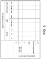
- Fig. 5 is an explanatory diagram showing an example of a table of defect parameters and background parameters according to this embodiment.
- Fig. 6 is an explanatory diagram showing an example of the display screen 70 according to the present embodiment.
- An image processing program 20 which causes a computer system to execute:
Landscapes
- Engineering & Computer Science (AREA)
- General Physics & Mathematics (AREA)
- Physics & Mathematics (AREA)
- Theoretical Computer Science (AREA)
- Quality & Reliability (AREA)
- Computer Vision & Pattern Recognition (AREA)
- Health & Medical Sciences (AREA)
- Analytical Chemistry (AREA)
- Biochemistry (AREA)
- General Health & Medical Sciences (AREA)
- Immunology (AREA)
- Pathology (AREA)
- Chemical & Material Sciences (AREA)
- Life Sciences & Earth Sciences (AREA)
- Image Processing (AREA)
- Investigating Materials By The Use Of Optical Means Adapted For Particular Applications (AREA)
- Image Analysis (AREA)
Abstract
Description
- The invention relates to an image processing device, an image processing method, and an image processing program.
- In the manufacturing field of industrial products, an inspection method of evaluating the presence or absence of defects in products or their degree through visual inspection that applies an image processing technique has been put into practical use. In this type of inspection field, an inspection accuracy is improved by application of machine learning, and for example, a method of detecting defects from an image of an inspection subject using a trained model trained to identify defect-specific feature images through a convolutional neural network is used. As a method of detecting a defect image by such machine learning, for example, as described in Patent Literature 1, there is a known visual inspection device that optimizes a threshold value for defining a condition for detecting a defect from an inspection subject, by comparing a registered image of a non-defective product with an image of the inspection subject.
- [Patent Literature 1]
Japanese Patent Laid-Open No. No. 2013-142558 - In such a visual inspection, although a detectable range (for example, a minimum width or a minimum area of a defect) of a defect image of a specific inspection subject under standard imaging conditions is known, when the imaging conditions change or the inspection subject changes, a way of seeing the defect (a reflected status of the defect) also changes. For example, when a contrast ratio between a defect and its background changes in response to a change in intensity of light that illuminates the inspection subject, a minimum width of the detectable defect can also change. Therefore, the performance equivalent to the detection performance of the defect image of a specific inspection subject under standard imaging conditions is not always exhibited under all imaging conditions and for all inspection subjects.
- As a means for verifying the detectable range of the defect image of all the inspection subjects under all imaging conditions, for example, it is conceivable to actually prepare a sample of a defective product and try to detect the defect image under all imaging conditions. However, preparation of such a sample is troublesome and it is difficult to cover all imaging conditions. Also, it is difficult to estimate the detectable range of the defect image of other inspection subjects under specific imaging conditions from the detectable range of the defect image of a specific inspection subject under standard imaging conditions.
- Therefore, an object of the invention is to provide an image processing device, an image processing method, and an image processing program capable of solving such a problem and verifying the detectable range of a defect image of an inspection subject under all imaging conditions.
- In order to solve the above-mentioned problems, an image processing device according to the invention includes a unit which superimposes a defect image on a background image with an original image of an inspection subject as the background image and performs image processing for altering a display format of the defect image or a display format of the background image, thereby generating a plurality of composite images having different ways of seeing the defect image with respect to the background image; a unit which verifies whether the defect image is detectable from each of the plurality of composite images; a unit which estimates a detectable range of the defect image based on a result of verifying whether the defect image is detectable; and a unit which displays the detectable range. By performing image processing for altering the display format of the defect image or the display format of the background image, it is possible to verify the detectable range of the defect image of all the inspection subjects under all imaging conditions.
- The image processing for altering the display format of the defect image may include a process of altering a shape of the defect image, a process of altering a position or a posture of the defect image with respect to the background image, a process of altering a size of the defect image, a process of enlarging or reducing the defect image, or a process of altering a ratio of a contrast of the defect image to that of the background image. By altering the display format of the defect image, the way of viewing the defect image with respect to the background image can be altered.
- The image processing for altering the display format of the background image may include a process of altering a texture pattern of the background image, a process of altering a brightness of the background image, a process of superimposing a noise pattern on the background image, a process of superimposing a shadow pattern on the background image, a process of rotating the background image with respect to the defect image, a process of enlarging or reducing the background image, or a process of altering the contrast ratio of the background image with respect to the defect image. By altering the display format of the background image, the way of viewing the defect image with respect to the background image can be altered.
- The image processing device according to the invention may further include a unit which sets a threshold value of a feature amount of the defect image which defines a condition for detecting the defect image as a defect, based on a detectable range. As a result, the threshold setting can be optimized.
- An image processing method according to the invention causes a computer system to execute a step of superimposing a defect image on a background image with an original image of an inspection subject as the background image and performing image processing for altering a display format of the defect image or a display format of the background image, thereby generating a plurality of composite images having different ways in which the defect image is seen with respect to the background image; a step of verifying whether the defect image is detachable from each of the plurality of composite images; a step of estimating a detectable range of the defect image based on a verifying result of whether the defect image is detectable; and a step of displaying the detectable range. By performing image processing for altering the display format of the defect image or the display format of the background image, it is possible to verify the detectable range of the defect image of all the inspection subjects under all imaging conditions.
- An image processing program according to the invention causes a computer system to execute a step of superimposing a defect image on a background image with an original image of an inspection subject as the background image and performing image processing for altering a display format of the defect image or a display format of the background image, thereby generating a plurality of composite images different ways of viewing the defect image with respect to the background image; a step of verifying whether the defect image is detachable from each of the plurality of composite images; a step of estimating a detectable range of the defect image based on a verifying result of whether the defect image is detectable; and a step of displaying the detectable range. By performing image processing for altering the display format of the defect image or the display format of the background image, it is possible to verify the detectable range of the defect image of all the inspection subjects under all imaging conditions.
- According to the invention, it is possible to verify the detectable range of a defect image of all the inspection subjects under all imaging conditions.
-
-
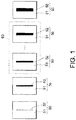
Fig. 1 is an explanatory view showing a summary of the image processing according to this embodiment. -
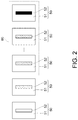
Fig. 2 is an explanatory view showing a summary of the image processing according to this embodiment. -
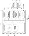
Fig. 3 is explanatory view showing an example of a hardware configuration of an image processing device according to this embodiment. -
Fig. 4 is an example of a flowchart showing the flow of image processing according to this embodiment. -
Fig. 5 is an explanatory view showing an example of a table of defect parameters and background parameters according to this embodiment. -
Fig. 6 is an explanatory view showing an example of a display screen according to this embodiment. - Hereinafter, embodiments according to an aspect of the invention will be described based on the drawings. The embodiments of the invention are intended to facilitate the understanding of the invention, and are not intended to limit the interpretation of the invention. The invention can be modified or improved without departing from the spirit thereof, and the invention also includes equivalents thereof. The same reference numerals indicate the same components, and repeated description will be omitted.
- First, an application example of the invention will be described referring to
Figs. 1 and2 . -
Figs. 1 and2 are explanatory views showing a summary of image processing according to the present embodiment. The image processing device superimposes adefect image 52 on thebackground image 51 by the use of an original image of an inspection subject as abackground image 51, and performs image processing of altering a display format of thedefect image 52 or a display format of thebackground image 51, thereby generating a plurality ofcomposite images 50 having different ways of seeing thedefect image 52 with respect to thebackground image 52. The inspection subject is, for example, a workpiece such as a device or a part. The type of thedefect image 52 may include, for example, "dirt", "scratch", "stain", and "dent". The image processing for altering the display format of thedefect image 52 includes, for example, a process of altering the shape of thedefect image 52, a process of altering the position or posture of thedefect image 52 with respect to thebackground image 51, a process of altering the size of thedefect image 52, a process of enlarging or reducing the size ofdefect image 52, or a process of altering a contrast ratio of thedefect image 52 to thebackground image 51. The image processing for altering the display format of thebackground image 51 includes a process of altering a texture pattern of thebackground image 51, a process of altering the brightness of thebackground image 51, a process of superimposing a noise pattern on thebackground image 51, a process of superimposing a shadow pattern on thebackground image 51, a process of rotating thebackground image 51 with respect to thedefect image 52, a process of enlarging or reducing thebackground image 51, or a process of altering the contrast ratio of thebackground image 51 to thedefect image 52. - In the example shown in
Fig. 1 , thedefect image 52 is a linear scratch, and a plurality ofcomposite images 50 in which the display format of thedefect image 52 is altered so that the line width gradually alters is generated. The image processing device verifies whether thedefect image 52 is detectable from each of the plurality ofcomposite images 50 shown inFig. 1 , and estimates thedetectable range 60 of thedefect image 52 based on the verification result. The example shown inFig. 1 shows that thedefect image 52 having a line width within thedetectable range 60 can be detected, and thedefect image 52 having a line width narrower than thedetectable range 60 and thedefect image 52 having a line width thicker than thedetection range 60 cannot be detected. When an algorithm for detecting the defect image is based on, for example, an algorithm for recognizing a feature image having a line width of a certain width or more as something other than a scratch, as shown inFig. 1 , an upper limit value can exist in the line width of the detectable scratch. In contrast, when the algorithm for detecting the defect image is based on, for example, an algorithm that recognizes all the feature images having a line width of a certain width or more as scratches, no upper limit value can exist in the line width of the detachable scratch. - On the other hand, in the example shown in
Fig. 2 , thedefect image 52 is a linear scratch, and a plurality ofcomposite images 50 in which the display format of thedefect image 52 is altered so that the contrast ratio of thedefect image 52 to thebackground image 51 gradually alters is generated. The image processing device verifies whether thedefect image 52 is detectable from each of the plurality ofcomposite images 50 shown inFig. 2 , and estimates thedetectable range 60 of thedefect image 52 based on the verification result. The example shown inFig. 2 shows that thedefect image 52 having a contrast ratio within thedetectable range 60 can be detected, and thedefect image 52 having a contrast ratio lower than thedetectable range 60 cannot be detected. - In this way, by variously altering the display format of the
defect image 52 or the display format of thebackground image 51, it is possible to verify thedetectable range 60 of thedefect image 52 of all the inspection subjects under all imaging conditions. The image processing device may display thedetectable range 60 of thedefect image 52 based on the verification result. As a result, the verifier can ascertain a degree of a detectable range of any kind of defect image of the inspection subject under any kind of imaging conditions. - The image processing device may automatically set a threshold value of the feature amount of the
defect image 52 that defines a condition for detecting thedefect image 52 as a defect based on thedetectable range 60. As a result, the setting of the threshold value can be optimized. For example, if the detectable range of linear scratch is the line width in the range of 3 to 20 pixels, the threshold value of the line width that defines the condition for being detected as a defect may be set in the range of 5 to 15 pixels. In this example, the feature amount of thedefect image 52 is the line width. In addition to the above-mentioned line width, the feature amount of thedefect image 52 may be an area, a ferret diameter, a circumscribed rectangular principal axis length, a circumscribed rectangular sub-axis length, a main axis angle, a circularity, a needle degree, a circumscribed circle diameter, an inscribed circle diameter, a perimeter, an equivalent ellipse main axis length, an equivalent ellipse sub-axis length, an equivalent ellipse main axis sub-axis ratio, an average brightness value, a maximum brightness value, a brightness or the like, depending on the features (a shape, a color, a brightness, etc.) of thedefect image 52. - Next, an example of the hardware configuration of the
image processing device 10 according to the present embodiment will be described with reference toFig. 3 . - The
image processing device 10 is a computer system equipped with aprocessor 11, amain memory 12, acamera interface 13, an input/output interface 14, adisplay interface 15, acommunication interface 16, and astorage device 17, as its hardware resources. - The
storage device 17 is a computer-readable recording medium such as a disk medium (for example, a magnetic recording medium or an optical magnetic recording medium) or a semiconductor memory (for example, a volatile memory or a non-volatile memory). Such a recording medium can also be called, for example, a non-transient recording medium. A software program (animage processing program 20 and an operating system 21) is stored in thestorage device 17. Theimage processing program 20 is a computer program for causing theprocessor 11 to execute the image processing method according to the present embodiment. When these software programs are read from thestorage device 17 into themain memory 12, and interpreted and executed by theprocessor 11, the image processing method according to the present embodiment is executed. - A
camera 41 is connected to thecamera interface 13. Thecamera 41 may include, for example, an image sensor that captures a color image. Thecamera 41 may be built into theimage processing device 10 or may be externally attached to theimage processing device 10. Thecamera 41 photographs an inspection subject. - The inspection subject may be, for example, a workpiece such as a device or a part which is conveyed by a belt conveyor on the production line. The
image processing device 10 may be installed on the production line, or may be installed at a place different from the production line. When theimage processing device 10 is installed at a place different from the production line, theimage processing device 10 may receive the image data obtained by photographing the inspection subject by the camera installed in the production line from a wired or wireless network through thecommunication interface 16. - An
input device 42 and anoutput device 43 are connected to the input/output interface 14. Theinput device 42 is a device that receives input of various settings of the inspector (for example, an operation which is input by the inspector through ascreen 70 shown inFig. 6 ). Theinput device 42 is, for example, a keyboard, a mouse, a touch pad, or the like. Theoutput device 43 is a device that outputs various processing results and the like. Theoutput device 43 is, for example, a printer. Adisplay 44 is connected to thedisplay interface 15. Thedisplay 44 is, for example, a liquid crystal display. -
Fig. 4 is an example of a flowchart showing the flow of image processing according to this embodiment. - In
step 401, theimage processing device 10 sets a parameter (hereinafter, referred to as "defect parameter") that specifies the display format of thedefect image 52. The defect parameters specify, for example, the shape of thedefect image 52, the position or posture of thedefect image 52 with respect to thebackground image 51, the size of thedefect image 52, the magnification ratio or reduction ratio of thedefect image 52, or the contrast ratio of thedefect image 52 to thebackground image 51. Theimage processing device 10 may set the defect parameter based on the input operation from the inspector, or may automatically set the defect parameter according to the rule defined by theimage processing program 20. - In
step 402, theimage processing device 10 sets a parameter (hereinafter, referred to as "background parameter") that specifies the display format of thebackground image 51. The background parameters specify, for example, the texture pattern of thebackground image 51, the noise pattern superimposed on thebackground image 51, the brightness of thebackground image 51, the shadow pattern superimposed on thebackground image 51, the rotation angle of thebackground image 51 with respect to thedefect image 52, the magnification ratio or reduction ratio of thebackground image 51, or the contrast ratio of thebackground image 51 to thedefect image 52. Theimage processing device 10 may set background parameters based on an input operation from the inspector, or may automatically set background parameters according to a rule defined by theimage processing program 20. - In
step 403, theimage processing device 10 superimposes thedefect image 52 on thebackground image 51 with the original image of the inspection subject as thebackground image 51, and performs the image processing of altering the display format of thedefect image 52 or the display format of thebackground image 51 based on the defect parameters and background parameters that are each set insteps composite images 50 having different ways of seeing thedefect image 52 with respect to thebackground image 51. For example, in the example shown inFig. 1 , the image processing is performed to alter the shape of thedefect image 52 so that the line width of thedefect image 52 alters. - Here, the original image of the inspection subject may be image data of the inspection subject of a non-defective product photographed by the
camera 41, or CAD (Computer Aided Design) data of the inspection subject. Further, thedefect image 52 may be image data of the defect extracted from the image data of the inspection subject of a defective product photographed by thecamera 41, may be image data artificially synthesized by CG (Computer Graphics), or may be the image data artificially synthesized by a painting process of an inspector. - In
step 404, theimage processing device 10 verifies whether thedefect image 52 is detectable from each of the plurality ofcomposite images 50. In this verification process, a general-purpose defect detection algorithm may be used. - In
step 405, theimage processing device 10 estimates thedetectable range 60 of thedefect image 52 based on the verification result ofstep 404. Thedetectable range 60 may be one of detectable upper limit value and lower limit value of the feature amount of thedefect image 52, and may be a range between such an upper limit value and a lower limit value. - In
step 406, theimage processing device 10 displays thedetectable range 60 estimated instep 405 on thedisplay 44. - In
step 407, theimage processing device 10 sets a threshold value of the feature amount of thedefect image 52 that defines the condition for detecting thedefect image 52 as a defect, based on thedetectable range 60 which is estimated instep 405. - In
step 408, theimage processing device 10 determines whether the verification of whether thedefect image 52 can be detected for all the combinations of the defect parameter and the background parameter which are set in each ofsteps -
Fig. 5 is an explanatory diagram showing an example of a table of defect parameters and background parameters according to this embodiment. - In this example, the defect parameters specify the shape of the defect image 52 (three types of "A" shape, "B" shape, and "C" shape), the size of the defect image 52 (three types of "large", "medium", and "small"), and the contrast ratio of the
defect image 52 to the background image 51 (three types of "high", "medium", and "low"). The background parameters specify the texture pattern of the background image 51 (three types of "X" pattern, "Y" pattern, and "Z" pattern), and the brightness of the background image 51 (three types of "high", "medium", and "low"). In this example, there are 9□6=54 combination patterns of defect parameters and background parameters, and the verification process ofstep 404 is executed for each combination. - Further, the verification process of
step 404 may be performed, while automatically altering the defect parameter or the background parameter according to a predetermined rule or irregularly (randomly) altering the defect parameter or the background parameter. Further, the verification process ofstep 404 may be performed, while finely altering the defect parameter or the background parameter in the vicinity of the detectable upper limit value or the lower limit value of the feature amount of thedefect image 52 and roughly altering the defect parameter or the background parameter in the other range. Further, the verification process ofstep 404 may be performed, while finely altering the defect parameter or the background parameter at uniform intervals between the detectable upper limit value and the lower limit value of the feature amount of thedefect image 52. -
Fig. 6 is an explanatory diagram showing an example of thedisplay screen 70 according to the present embodiment. - The
display screen 70 is an example of a screen displayed on thedisplay 44 when verifying whether thedefect image 52 can be detected.Reference numeral 71 indicates a window for displaying a plurality of evaluation items of thedefect image 52. The evaluation items are, for example, items such as "line width", "brightness", and "contrast ratio" of thedefect image 52. For example, when the evaluation item of "line width" is selected by the inspector, whether thedefect image 52 can be detected is verified for various line widths of thedefect image 52.Reference numeral 72 indicates a button instructing execution of verification for the evaluation item selected from thewindow 71.Reference numeral 74 indicates a list of all thecomposite images 50 generated at the time of verification of the evaluation items selected from thewindow 71.Reference numeral 75 indicates a list of thecomposite images 50 within the detectable range of thedefect image 52 among all thecomposite images 50 generated at the time of verification.Reference numeral 73 indicates a button instructing that the threshold value of the feature amount of thedefect image 52 is automatically set based on thedetectable range 60. - The
image processing device 10 functions as a means for executing the above-mentioned image processing method (steps 401 to 408 ofFig. 4 ), and such means does not need to be necessarily realized by collaboration of the hardware resources of theimage processing device 10 and theimage processing program 20, and may be realized by, for example, the use of a dedicated hardware resource of the image processing device 10 (for example, an application specific integrated circuit (ASIC), a field programmable gate array (FPGA) or the like). Theimage processing program 20 may include a software module that executes each of thesteps 401 to 408 of the above-mentioned image processing method. - A part or all of the above-described embodiments may be described as the following appendix, but are not limited to the following.
- An
image processing device 10 including: - an
image processing unit 403 which superimposes thedefect image 52 on thebackground image 51 with the original image of the inspection subject as thebackground image 51 and performs image processing for altering the display format of thedefect image 52 or the display format of thebackground image 51, thereby generating a plurality ofcomposite images 50 having different ways of seeing thedefect image 52 with respect to thebackground image 51; - a
verification unit 404 which verifies whether thedefect image 52 is detectable from each of the plurality ofcomposite images 50; - an
estimation unit 405 which estimates thedetectable range 60 of thedefect image 52 based on a verifying result of whether the defect image is detectable; and - a
display unit 406 which displays thedetectable range 60. - The
image processing device 10 described in Appendix 1, in which the image processing for altering the display format of thedefect image 52 includes: - a process of altering the shape of the
defect image 52, - a process of altering a position or a posture of the
defect image 52 with respect to thebackground image 51, - a process of altering the size of the
defect image 52, - a process of enlarging or reducing the
defect image 52, or - a process of altering a contrast ratio of the
defect image 52 to thebackground image 51. - The
image processing device 10 described in Appendix 1 or 2, in which the image processing for altering the display format of thebackground image 51 includes: - a process of altering a texture pattern of the
background image 51, - a process of altering a brightness of the
background image 51, - a process of superimposing a noise pattern on the
background image 51, - a process of superimposing a shadow pattern on the
background image 51, - a process of rotating the
background image 51 with respect to thedefect image 52, - a process of enlarging or reducing the
background image 51, or - a process of altering the contrast ratio of the
background image 51 to thedefect image 52. - The
image processing device 10 described in any one of Appendices 1 to 3, further including a setting unit which sets a threshold value of a feature amount of thedefect image 52 which defines a condition for detecting thedefect image 52 as a defect, based on adetectable range 60. - An image processing method of causing a computer system to execute:
- a
step 403 of superimposing thedefect image 52 on thebackground image 51 with the original image of the inspection subject as thebackground image 51 and performing image processing for altering the display format of thedefect image 52 or the display format of thebackground image 51, thereby generating a plurality ofcomposite images 50 having different ways of seeing thedefect image 52 with respect to thebackground image 51; - a
step 404 of verifying whether thedefect image 52 is detectable from each of the plurality ofcomposite images 50; - a
step 405 of estimating thedetectable range 60 of thedefect image 52 based on a verifying result of whether the defect image is detectable; and - a
step 406 of displaying thedetectable range 60. - An
image processing program 20 which causes a computer system to execute: - a
step 403 of superimposing thedefect image 52 on thebackground image 51 with the original image of the inspection subject as thebackground image 51 and performing image processing for altering the display format of thedefect image 52 or the display format of thebackground image 51, thereby generating a plurality ofcomposite images 50 having different ways of seeing thedefect image 52 with respect to thebackground image 51; - a
step 404 of verifying whether thedefect image 52 is detectable from each of the plurality ofcomposite images 50; - a
step 405 of estimating thedetectable range 60 of thedefect image 52 based on a verifying result of whether the defect image is detectable; and - a
step 406 of displaying thedetectable range 60. -
- 10
- Image processing device
- 11
- Processor
- 12
- Main memory
- 13
- Camera interface
- 14
- Input/output interface
- 15
- Display interface
- 16
- Communication interface
- 17
- Storage device
- 20
- Image processing program
- 21
- Operating system
- 41
- Camera
- 42
- Input device
- 43
- Output device
- 44
- Display
- 50
- Composite image
- 51
- Background image
- 52
- Defect image
- 60
- Detectable range
- 70
- Display screen
Claims (6)
- An image processing device, comprising:a unit which superimposes a defect image on a background image with an original image of an inspection subject as the background image and performs image processing for altering a display format of the defect image or a display format of the background image, thereby generating a plurality of composite images having different ways of seeing the defect image with respect to the background image;a unit which verifies whether the defect image is detachable from each of the plurality of composite images;a unit which estimates a detectable range of the defect image based on a verifying result of whether the defect image is detectable; anda unit which displays the detectable range.
- The image processing device according to claim 1,
wherein the image processing for altering the display format of the defect image comprises:a process of altering a shape of the defect image,a process of altering a position or a posture of the defect image with respect to the background image,a process of altering a size of the defect image,a process of enlarging or reducing the defect image, ora process of altering a contrast ratio of the defect image to the background image. - The image processing device according to claim 1 or 2,
wherein the image processing for altering the display format of the background image comprises:a process of altering a texture pattern of the background image,a process of altering a brightness of the background image,a process of superimposing a noise pattern on the background image,a process of superimposing a shadow pattern on the background image,a process of rotating the background image with respect to the defect image,a process of enlarging or reducing the background image, ora process of altering a contrast ratio of the background image with respect to the defect image. - The image processing device according to any one of claims 1 to 3, further comprising:
a unit which sets a threshold value of a feature amount of the defect image which defines a condition for detecting the defect image as a defect, based on a detectable range. - An image processing method of causing a computer system to execute:a step of superimposing a defect image on a background image with an original image of an inspection subject as the background image and performing image processing for altering a display format of the defect image or a display format of the background image, thereby generating a plurality of composite images having different ways of seeing the defect image with respect to the background image;a step of verifying whether the defect image is detachable from each of the plurality of composite images;a step of estimating a detectable range of the defect image based on a verifying result of whether the defect image is detectable; anda step of displaying the detectable range.
- An image processing program which causes a computer system to execute:a step of superimposing a defect image on a background image with an original image of an inspection subject as the background image and performing image processing for altering a display format of the defect image or a display format of the background image, thereby generating a plurality of composite images having different ways of seeing the defect image with respect to the background image;a step of verifying whether the defect image is detachable from each of the plurality of composite images;a step of estimating a detectable range of the defect image based on a verifying result of whether the defect image is detectable; anda step of displaying the detectable range.
Applications Claiming Priority (2)
| Application Number | Priority Date | Filing Date | Title |
|---|---|---|---|
| JP2018247166A JP2020106469A (en) | 2018-12-28 | 2018-12-28 | Image processing apparatus, image processing method, and image processing program |
| PCT/JP2019/041426 WO2020137121A1 (en) | 2018-12-28 | 2019-10-23 | Image processing device, image processing method, and image processing program |
Publications (3)
| Publication Number | Publication Date |
|---|---|
| EP3904865A1 true EP3904865A1 (en) | 2021-11-03 |
| EP3904865A4 EP3904865A4 (en) | 2022-11-02 |
| EP3904865B1 EP3904865B1 (en) | 2026-03-25 |
Family
ID=71128909
Family Applications (1)
| Application Number | Title | Priority Date | Filing Date |
|---|---|---|---|
| EP19901921.7A Active EP3904865B1 (en) | 2018-12-28 | 2019-10-23 | Image processing device, image processing method, and image processing program |
Country Status (5)
| Country | Link |
|---|---|
| US (1) | US11769248B2 (en) |
| EP (1) | EP3904865B1 (en) |
| JP (2) | JP2020106469A (en) |
| CN (1) | CN112534245B (en) |
| WO (1) | WO2020137121A1 (en) |
Families Citing this family (8)
| Publication number | Priority date | Publication date | Assignee | Title |
|---|---|---|---|---|
| JP7258509B2 (en) * | 2018-10-15 | 2023-04-17 | オムロン株式会社 | Image processing device, image processing method, and image processing program |
| JP7281041B2 (en) * | 2018-11-29 | 2023-05-25 | 京セラドキュメントソリューションズ株式会社 | Type discrimination system |
| JP7518784B2 (en) * | 2021-03-05 | 2024-07-18 | 日立Astemo株式会社 | Visual inspection apparatus, visual inspection method, image generating apparatus, and image generating method |
| WO2022224657A1 (en) * | 2021-04-19 | 2022-10-27 | 富士フイルム株式会社 | Device, method, and program for detecting signs of abnormality in production line, production device, and inspection device |
| WO2023139688A1 (en) * | 2022-01-19 | 2023-07-27 | 三菱重工エンジン&ターボチャージャ株式会社 | Fault diagnosis model creation device, fault diagnosis model creation method, and fault diagnosis model creation program |
| JP7642576B2 (en) * | 2022-02-07 | 2025-03-10 | アンリツ株式会社 | Inspection device, learning model generation method, and inspection method |
| KR102870463B1 (en) * | 2024-12-20 | 2025-10-13 | 재단법인 포항산업과학연구원 | Method and apparatus for detecting defect in steel plate |
| CN120355717B (en) * | 2025-06-24 | 2025-09-05 | 浙江双元科技股份有限公司 | Full-automatic camera-level error testing method and system based on simulation defects |
Family Cites Families (14)
| Publication number | Priority date | Publication date | Assignee | Title |
|---|---|---|---|---|
| JPH1114553A (en) * | 1997-06-23 | 1999-01-22 | Omron Corp | Method and apparatus for outputting defect sample data in visual defect inspection apparatus |
| CN100428277C (en) | 1999-11-29 | 2008-10-22 | 奥林巴斯光学工业株式会社 | Defect inspection system |
| JP4288415B2 (en) * | 2003-05-12 | 2009-07-01 | 日本電気株式会社 | Method, system, apparatus, and program for creating defect data for reticle inspection apparatus evaluation |
| JP2008203034A (en) * | 2007-02-19 | 2008-09-04 | Olympus Corp | Defect detection device and method |
| JP2011047724A (en) * | 2009-08-26 | 2011-03-10 | Hitachi High-Technologies Corp | Apparatus and method for inspecting defect |
| JP2013019866A (en) * | 2011-07-14 | 2013-01-31 | Hitachi High-Technologies Corp | Scanning electron microscope, defect inspection system, and defect inspection apparatus |
| JP5865707B2 (en) | 2012-01-06 | 2016-02-17 | 株式会社キーエンス | Appearance inspection apparatus, appearance inspection method, and computer program |
| JP2013257197A (en) * | 2012-06-12 | 2013-12-26 | Toppan Printing Co Ltd | Performance evaluation sheet for printed matter inspection device |
| JP6447691B2 (en) * | 2012-08-02 | 2019-01-09 | 株式会社リコー | Image inspection system and image inspection method |
| JP6241121B2 (en) | 2012-09-14 | 2017-12-06 | 株式会社リコー | Image inspection apparatus, image inspection system, and image inspection method |
| JP2015142181A (en) * | 2014-01-27 | 2015-08-03 | キヤノン株式会社 | Control device and control method |
| DE102014004556A1 (en) * | 2014-03-31 | 2015-10-01 | Heidelberger Druckmaschinen Ag | Method for checking the reliability of error detection of an image inspection method |
| JP6235684B1 (en) * | 2016-11-29 | 2017-11-22 | Ckd株式会社 | Inspection device and PTP packaging machine |
| JP7254324B2 (en) * | 2017-06-05 | 2023-04-10 | 学校法人梅村学園 | IMAGE GENERATING APPARATUS AND IMAGE GENERATING METHOD FOR GENERATING INSPECTION IMAGE FOR PERFORMANCE ADJUSTMENT OF IMAGE INSPECTION SYSTEM |
-
2018
- 2018-12-28 JP JP2018247166A patent/JP2020106469A/en active Pending
-
2019
- 2019-10-23 CN CN201980051518.9A patent/CN112534245B/en active Active
- 2019-10-23 US US17/270,441 patent/US11769248B2/en active Active
- 2019-10-23 EP EP19901921.7A patent/EP3904865B1/en active Active
- 2019-10-23 WO PCT/JP2019/041426 patent/WO2020137121A1/en not_active Ceased
-
2022
- 2022-11-29 JP JP2022190277A patent/JP7397415B2/en active Active
Also Published As
| Publication number | Publication date |
|---|---|
| WO2020137121A1 (en) | 2020-07-02 |
| JP2020106469A (en) | 2020-07-09 |
| CN112534245B (en) | 2024-06-28 |
| EP3904865A4 (en) | 2022-11-02 |
| US20210183037A1 (en) | 2021-06-17 |
| CN112534245A (en) | 2021-03-19 |
| JP2023024482A (en) | 2023-02-16 |
| JP7397415B2 (en) | 2023-12-13 |
| EP3904865B1 (en) | 2026-03-25 |
| US11769248B2 (en) | 2023-09-26 |
Similar Documents
| Publication | Publication Date | Title |
|---|---|---|
| US11769248B2 (en) | Image processing device, image processing method, and image processing non-transitory computer readable medium for verifying detectable range of defect image | |
| TWI910278B (en) | Image augmentation techniques for automated visual inspection | |
| CN112577969B (en) | Defect detection method and defect detection system based on machine vision | |
| US11317067B2 (en) | Method and system for inspecting display image | |
| US7881520B2 (en) | Defect inspection system | |
| JP2013224833A (en) | Visual inspection device, visual inspection method and computer program | |
| US12315135B2 (en) | Transmission image-based non-destructive inspecting method, method of providing non-destructive inspection function, and device therefor | |
| CN115203815A (en) | Production speed component inspection system and method | |
| TWI753424B (en) | Appearance inspection management system, appearance inspection management device, appearance inspection management method, and program | |
| JP2007114843A (en) | Pass / fail judgment device | |
| Ghidoni et al. | Automatic color inspection for colored wires in electric cables | |
| KR101748768B1 (en) | Image generating method and apparatus for machine vision test, method and apparatus for simulating machine vision test, and machine vision testing system | |
| JP7127046B2 (en) | System and method for 3D profile determination using model-based peak selection | |
| US20210233231A1 (en) | Image processing device, image processing method, and computer readable recording medium | |
| WO2022201968A1 (en) | Information processing device, control program, and control method | |
| CN116703912B (en) | Mini-host network port integrity visual detection method | |
| CN110274911B (en) | Image processing system, image processing device, storage medium | |
| CN117788444A (en) | SMT patch offset detection method, SMT patch offset detection device and SMT patch offset detection system | |
| US20250014166A1 (en) | System, image processing method, and program | |
| JP2018173732A (en) | Inspection device, inspection method, inspection program, and recording medium | |
| CN121213447A (en) | Line detection method and device | |
| CN115761488A (en) | Method, device and system for detecting deviation of conveyor belt | |
| WO2024095721A1 (en) | Image processing device and image processing method | |
| KR20190042180A (en) | Cover-glass analyzing method | |
| CN116897282A (en) | Image display device, image display method and program |
Legal Events
| Date | Code | Title | Description |
|---|---|---|---|
| STAA | Information on the status of an ep patent application or granted ep patent |
Free format text: STATUS: THE INTERNATIONAL PUBLICATION HAS BEEN MADE |
|
| PUAI | Public reference made under article 153(3) epc to a published international application that has entered the european phase |
Free format text: ORIGINAL CODE: 0009012 |
|
| STAA | Information on the status of an ep patent application or granted ep patent |
Free format text: STATUS: REQUEST FOR EXAMINATION WAS MADE |
|
| 17P | Request for examination filed |
Effective date: 20210212 |
|
| AK | Designated contracting states |
Kind code of ref document: A1 Designated state(s): AL AT BE BG CH CY CZ DE DK EE ES FI FR GB GR HR HU IE IS IT LI LT LU LV MC MK MT NL NO PL PT RO RS SE SI SK SM TR |
|
| DAV | Request for validation of the european patent (deleted) | ||
| DAX | Request for extension of the european patent (deleted) | ||
| A4 | Supplementary search report drawn up and despatched |
Effective date: 20221006 |
|
| RIC1 | Information provided on ipc code assigned before grant |
Ipc: G06T 7/00 20170101ALI20220929BHEP Ipc: G01N 21/88 20060101AFI20220929BHEP |
|
| GRAP | Despatch of communication of intention to grant a patent |
Free format text: ORIGINAL CODE: EPIDOSNIGR1 |
|
| STAA | Information on the status of an ep patent application or granted ep patent |
Free format text: STATUS: GRANT OF PATENT IS INTENDED |
|
| INTG | Intention to grant announced |
Effective date: 20251020 |
|
| GRAS | Grant fee paid |
Free format text: ORIGINAL CODE: EPIDOSNIGR3 |
|
| GRAA | (expected) grant |
Free format text: ORIGINAL CODE: 0009210 |
|
| STAA | Information on the status of an ep patent application or granted ep patent |
Free format text: STATUS: THE PATENT HAS BEEN GRANTED |
|
| AK | Designated contracting states |
Kind code of ref document: B1 Designated state(s): AL AT BE BG CH CY CZ DE DK EE ES FI FR GB GR HR HU IE IS IT LI LT LU LV MC MK MT NL NO PL PT RO RS SE SI SK SM TR |
|
| REG | Reference to a national code |
Ref country code: CH Ref legal event code: F10 Free format text: ST27 STATUS EVENT CODE: U-0-0-F10-F00 (AS PROVIDED BY THE NATIONAL OFFICE) Effective date: 20260325 Ref country code: GB Ref legal event code: FG4D |
|
| REG | Reference to a national code |
Ref country code: DE Ref legal event code: R096 Ref document number: 602019082965 Country of ref document: DE |
|
| REG | Reference to a national code |
Ref country code: IE Ref legal event code: FG4D |