EP3903377B1 - Electronic device including expanded flexible printed circuit board antenna module - Google Patents
Electronic device including expanded flexible printed circuit board antenna module Download PDFInfo
- Publication number
- EP3903377B1 EP3903377B1 EP20778501.5A EP20778501A EP3903377B1 EP 3903377 B1 EP3903377 B1 EP 3903377B1 EP 20778501 A EP20778501 A EP 20778501A EP 3903377 B1 EP3903377 B1 EP 3903377B1
- Authority
- EP
- European Patent Office
- Prior art keywords
- electronic device
- module
- radiating sheet
- antenna module
- pattern
- Prior art date
- Legal status (The legal status is an assumption and is not a legal conclusion. Google has not performed a legal analysis and makes no representation as to the accuracy of the status listed.)
- Active
Links
Images




Classifications
-
- H—ELECTRICITY
- H01—ELECTRIC ELEMENTS
- H01Q—ANTENNAS, i.e. RADIO AERIALS
- H01Q1/00—Details of, or arrangements associated with, antennas
- H01Q1/02—Arrangements for de-icing; Arrangements for drying-out ; Arrangements for cooling; Arrangements for preventing corrosion
-
- G—PHYSICS
- G06—COMPUTING OR CALCULATING; COUNTING
- G06F—ELECTRIC DIGITAL DATA PROCESSING
- G06F1/00—Details not covered by groups G06F3/00 - G06F13/00 and G06F21/00
- G06F1/16—Constructional details or arrangements
- G06F1/1613—Constructional details or arrangements for portable computers
- G06F1/1633—Constructional details or arrangements of portable computers not specific to the type of enclosures covered by groups G06F1/1615 - G06F1/1626
- G06F1/1635—Details related to the integration of battery packs and other power supplies such as fuel cells or integrated AC adapter
-
- H—ELECTRICITY
- H01—ELECTRIC ELEMENTS
- H01Q—ANTENNAS, i.e. RADIO AERIALS
- H01Q1/00—Details of, or arrangements associated with, antennas
- H01Q1/12—Supports; Mounting means
- H01Q1/22—Supports; Mounting means by structural association with other equipment or articles
- H01Q1/2208—Supports; Mounting means by structural association with other equipment or articles associated with components used in interrogation type services, i.e. in systems for information exchange between an interrogator/reader and a tag/transponder, e.g. in Radio Frequency Identification [RFID] systems
-
- H—ELECTRICITY
- H01—ELECTRIC ELEMENTS
- H01Q—ANTENNAS, i.e. RADIO AERIALS
- H01Q1/00—Details of, or arrangements associated with, antennas
- H01Q1/12—Supports; Mounting means
- H01Q1/22—Supports; Mounting means by structural association with other equipment or articles
- H01Q1/24—Supports; Mounting means by structural association with other equipment or articles with receiving set
- H01Q1/241—Supports; Mounting means by structural association with other equipment or articles with receiving set used in mobile communications, e.g. GSM
- H01Q1/242—Supports; Mounting means by structural association with other equipment or articles with receiving set used in mobile communications, e.g. GSM specially adapted for hand-held use
- H01Q1/243—Supports; Mounting means by structural association with other equipment or articles with receiving set used in mobile communications, e.g. GSM specially adapted for hand-held use with built-in antennas
-
- H—ELECTRICITY
- H01—ELECTRIC ELEMENTS
- H01Q—ANTENNAS, i.e. RADIO AERIALS
- H01Q1/00—Details of, or arrangements associated with, antennas
- H01Q1/36—Structural form of radiating elements, e.g. cone, spiral, umbrella; Particular materials used therewith
- H01Q1/38—Structural form of radiating elements, e.g. cone, spiral, umbrella; Particular materials used therewith formed by a conductive layer on an insulating support
-
- H—ELECTRICITY
- H01—ELECTRIC ELEMENTS
- H01Q—ANTENNAS, i.e. RADIO AERIALS
- H01Q1/00—Details of, or arrangements associated with, antennas
- H01Q1/40—Radiating elements coated with or embedded in protective material
-
- H—ELECTRICITY
- H01—ELECTRIC ELEMENTS
- H01Q—ANTENNAS, i.e. RADIO AERIALS
- H01Q1/00—Details of, or arrangements associated with, antennas
- H01Q1/52—Means for reducing coupling between antennas; Means for reducing coupling between an antenna and another structure
- H01Q1/526—Electromagnetic shields
-
- H—ELECTRICITY
- H04—ELECTRIC COMMUNICATION TECHNIQUE
- H04B—TRANSMISSION
- H04B1/00—Details of transmission systems, not covered by a single one of groups H04B3/00 - H04B13/00; Details of transmission systems not characterised by the medium used for transmission
- H04B1/38—Transceivers, i.e. devices in which transmitter and receiver form a structural unit and in which at least one part is used for functions of transmitting and receiving
- H04B1/3827—Portable transceivers
- H04B1/3888—Arrangements for carrying or protecting transceivers
-
- H—ELECTRICITY
- H04—ELECTRIC COMMUNICATION TECHNIQUE
- H04M—TELEPHONIC COMMUNICATION
- H04M1/00—Substation equipment, e.g. for use by subscribers
- H04M1/02—Constructional features of telephone sets
- H04M1/0202—Portable telephone sets, e.g. cordless phones, mobile phones or bar type handsets
- H04M1/026—Details of the structure or mounting of specific components
- H04M1/0277—Details of the structure or mounting of specific components for a printed circuit board assembly
-
- H—ELECTRICITY
- H05—ELECTRIC TECHNIQUES NOT OTHERWISE PROVIDED FOR
- H05K—PRINTED CIRCUITS; CASINGS OR CONSTRUCTIONAL DETAILS OF ELECTRIC APPARATUS; MANUFACTURE OF ASSEMBLAGES OF ELECTRICAL COMPONENTS
- H05K1/00—Printed circuits
- H05K1/02—Details
- H05K1/0277—Bendability or stretchability details
- H05K1/028—Bending or folding regions of flexible printed circuits
-
- H—ELECTRICITY
- H05—ELECTRIC TECHNIQUES NOT OTHERWISE PROVIDED FOR
- H05K—PRINTED CIRCUITS; CASINGS OR CONSTRUCTIONAL DETAILS OF ELECTRIC APPARATUS; MANUFACTURE OF ASSEMBLAGES OF ELECTRICAL COMPONENTS
- H05K1/00—Printed circuits
- H05K1/02—Details
- H05K1/11—Printed elements for providing electric connections to or between printed circuits
- H05K1/118—Printed elements for providing electric connections to or between printed circuits specially for flexible printed circuits, e.g. using folded portions
-
- H—ELECTRICITY
- H05—ELECTRIC TECHNIQUES NOT OTHERWISE PROVIDED FOR
- H05K—PRINTED CIRCUITS; CASINGS OR CONSTRUCTIONAL DETAILS OF ELECTRIC APPARATUS; MANUFACTURE OF ASSEMBLAGES OF ELECTRICAL COMPONENTS
- H05K1/00—Printed circuits
- H05K1/02—Details
- H05K1/14—Structural association of two or more printed circuits
- H05K1/147—Structural association of two or more printed circuits at least one of the printed circuits being bent or folded, e.g. by using a flexible printed circuit
-
- H—ELECTRICITY
- H05—ELECTRIC TECHNIQUES NOT OTHERWISE PROVIDED FOR
- H05K—PRINTED CIRCUITS; CASINGS OR CONSTRUCTIONAL DETAILS OF ELECTRIC APPARATUS; MANUFACTURE OF ASSEMBLAGES OF ELECTRICAL COMPONENTS
- H05K1/00—Printed circuits
- H05K1/16—Printed circuits incorporating printed electric components, e.g. printed resistors, capacitors or inductors
- H05K1/165—Printed circuits incorporating printed electric components, e.g. printed resistors, capacitors or inductors incorporating printed inductors
-
- H—ELECTRICITY
- H05—ELECTRIC TECHNIQUES NOT OTHERWISE PROVIDED FOR
- H05K—PRINTED CIRCUITS; CASINGS OR CONSTRUCTIONAL DETAILS OF ELECTRIC APPARATUS; MANUFACTURE OF ASSEMBLAGES OF ELECTRICAL COMPONENTS
- H05K3/00—Apparatus or processes for manufacturing printed circuits
- H05K3/36—Assembling printed circuits with other printed circuits
- H05K3/361—Assembling flexible printed circuits with other printed circuits
-
- B—PERFORMING OPERATIONS; TRANSPORTING
- B82—NANOTECHNOLOGY
- B82Y—SPECIFIC USES OR APPLICATIONS OF NANOSTRUCTURES; MEASUREMENT OR ANALYSIS OF NANOSTRUCTURES; MANUFACTURE OR TREATMENT OF NANOSTRUCTURES
- B82Y10/00—Nanotechnology for information processing, storage or transmission, e.g. quantum computing or single electron logic
-
- H—ELECTRICITY
- H05—ELECTRIC TECHNIQUES NOT OTHERWISE PROVIDED FOR
- H05K—PRINTED CIRCUITS; CASINGS OR CONSTRUCTIONAL DETAILS OF ELECTRIC APPARATUS; MANUFACTURE OF ASSEMBLAGES OF ELECTRICAL COMPONENTS
- H05K1/00—Printed circuits
- H05K1/02—Details
- H05K1/0213—Electrical arrangements not otherwise provided for
- H05K1/0216—Reduction of cross-talk, noise or electromagnetic interference
- H05K1/0218—Reduction of cross-talk, noise or electromagnetic interference by printed shielding conductors, ground planes or power plane
- H05K1/0224—Patterned shielding planes, ground planes or power planes
-
- H—ELECTRICITY
- H05—ELECTRIC TECHNIQUES NOT OTHERWISE PROVIDED FOR
- H05K—PRINTED CIRCUITS; CASINGS OR CONSTRUCTIONAL DETAILS OF ELECTRIC APPARATUS; MANUFACTURE OF ASSEMBLAGES OF ELECTRICAL COMPONENTS
- H05K1/00—Printed circuits
- H05K1/02—Details
- H05K1/03—Use of materials for the substrate
- H05K1/0393—Flexible materials
-
- H—ELECTRICITY
- H05—ELECTRIC TECHNIQUES NOT OTHERWISE PROVIDED FOR
- H05K—PRINTED CIRCUITS; CASINGS OR CONSTRUCTIONAL DETAILS OF ELECTRIC APPARATUS; MANUFACTURE OF ASSEMBLAGES OF ELECTRICAL COMPONENTS
- H05K2201/00—Indexing scheme relating to printed circuits covered by H05K1/00
- H05K2201/04—Assemblies of printed circuits
- H05K2201/042—Stacked spaced PCBs; Planar parts of folded flexible circuits having mounted components in between or spaced from each other
-
- H—ELECTRICITY
- H05—ELECTRIC TECHNIQUES NOT OTHERWISE PROVIDED FOR
- H05K—PRINTED CIRCUITS; CASINGS OR CONSTRUCTIONAL DETAILS OF ELECTRIC APPARATUS; MANUFACTURE OF ASSEMBLAGES OF ELECTRICAL COMPONENTS
- H05K2201/00—Indexing scheme relating to printed circuits covered by H05K1/00
- H05K2201/05—Flexible printed circuits [FPCs]
-
- H—ELECTRICITY
- H05—ELECTRIC TECHNIQUES NOT OTHERWISE PROVIDED FOR
- H05K—PRINTED CIRCUITS; CASINGS OR CONSTRUCTIONAL DETAILS OF ELECTRIC APPARATUS; MANUFACTURE OF ASSEMBLAGES OF ELECTRICAL COMPONENTS
- H05K2201/00—Indexing scheme relating to printed circuits covered by H05K1/00
- H05K2201/09—Shape and layout
- H05K2201/09209—Shape and layout details of conductors
- H05K2201/09218—Conductive traces
-
- H—ELECTRICITY
- H05—ELECTRIC TECHNIQUES NOT OTHERWISE PROVIDED FOR
- H05K—PRINTED CIRCUITS; CASINGS OR CONSTRUCTIONAL DETAILS OF ELECTRIC APPARATUS; MANUFACTURE OF ASSEMBLAGES OF ELECTRICAL COMPONENTS
- H05K2201/00—Indexing scheme relating to printed circuits covered by H05K1/00
- H05K2201/10—Details of components or other objects attached to or integrated in a printed circuit board
- H05K2201/10007—Types of components
- H05K2201/10098—Components for radio transmission, e.g. radio frequency identification [RFID] tag, printed or non-printed antennas
Definitions
- a flexible printed circuit board is a thin and lightweight board that can fit into small spaces and be formed into specific shapes.
- An FPCB includes a conductive strip, such as a copper strip, and a nonconductive material, such as polyimide, surrounding the conductive strip.
- An FPCB is an electronic component for overcoming the weaknesses of an existing printed circuit board (PCB) in order to satisfy the trend toward compact and complex electronic products.
- a radiating sheet is generally used for electronic products requiring light weight and slimness.
- electronic components are disposed in a housing of an electronic device.
- heat may be generated in the electronic components (e.g., a wireless charging antenna, a processor, a speaker, and the like).
- a radiating sheet may be attached to the electronic components.
- the radiating sheet may be damaged by a relative movement between the plurality of electronic components.
- heat may accumulate in the electronic components, thus degrading the electronic components.
- computer readable medium includes any type of medium capable of being accessed by a computer, such as read only memory (ROM), random access memory (RAM), a hard disk drive, a compact disc (CD), a digital video disc (DVD), or any other type of memory.
- ROM read only memory
- RAM random access memory
- CD compact disc
- DVD digital video disc
- a "non-transitory” computer readable medium excludes wired, wireless, optical, or other communication links that transport transitory electrical or other signals.
- a non-transitory computer readable medium includes media where data can be permanently stored and media where data can be stored and later overwritten, such as a rewritable optical disc or an erasable memory device.
- FIGS. 1 through 11 discussed below, and the various embodiments used to describe the principles of the present disclosure in this patent document are by way of illustration only and should not be construed in any way to limit the scope of the disclosure. Those skilled in the art will understand that the principles of the present disclosure may be implemented in any suitably arranged system or device.
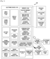
- FIG. 1 illustrates, in block diagram format, an example of an electronic device 101 in a network environment 100 according to various embodiments.
- the electronic device 101 in the network environment 100 may communicate with an electronic device 102 via a first network 198 (e.g., a short-range wireless communication network), or an electronic device 104 or a server 108 via a second network 199 (e.g., a long-range wireless communication network).
- the electronic device 101 may communicate with the electronic device 104 via the server 108.
- the processor 120 may execute, for example, software (e.g., a program 140) to control at least one other component (e.g., a hardware or software component) of the electronic device 101 coupled with the processor 120, and may perform various data processing or computation. According to one embodiment, as at least part of the data processing or computation, the processor 120 may load a command or data received from another component (e.g., the sensor module 176 or the communication module 190) in volatile memory 132, process the command or the data stored in the volatile memory 132, and store resulting data in non-volatile memory 134.
- software e.g., a program 140
- the processor 120 may load a command or data received from another component (e.g., the sensor module 176 or the communication module 190) in volatile memory 132, process the command or the data stored in the volatile memory 132, and store resulting data in non-volatile memory 134.
- the processor 120 may include a main processor 121 (e.g., a central processing unit (CPU) or an application processor (AP)), and an auxiliary processor 123 (e.g., a graphics processing unit (GPU), an image signal processor (ISP), a sensor hub processor, or a communication processor (CP)) that is operable independently from, or in conjunction with, the main processor 121.
- auxiliary processor 123 e.g., a graphics processing unit (GPU), an image signal processor (ISP), a sensor hub processor, or a communication processor (CP)
- the auxiliary processor 123 may be adapted to consume less power than the main processor 121, or to be specific to a specified function.
- the auxiliary processor 123 may be implemented as separate from, or as part of the main processor 121.
- the audio module 170 may convert a sound into an electrical signal and vice versa. According to certain embodiments, the audio module 170 may obtain the sound via the input device 150, or output the sound via the sound output device 155 or a headphone of an external electronic device (e.g., an electronic device 102) directly (e.g., through a physical coupling, such as a wire) or wirelessly coupled with the electronic device 101.
- an external electronic device e.g., an electronic device 102
- directly e.g., through a physical coupling, such as a wire
- the sensor module 176 may detect an operational state (e.g., power or temperature) of the electronic device 101 or an environmental state (e.g., a state of a user) external to the electronic device 101, and then generate an electrical signal or data value corresponding to the detected state.
- the sensor module 176 may include, for example, a gesture sensor, a gyro sensor, an atmospheric pressure sensor, a magnetic sensor, an acceleration sensor, a grip sensor, a proximity sensor, a color sensor, an infrared (IR) sensor, a biometric sensor, a temperature sensor, a humidity sensor, or an illuminance sensor.
- a corresponding one of these communication modules may communicate with the external electronic device via the first network 198 (e.g., a short-range communication network, such as BLUETOOTH TM , wireless-fidelity (WI-FI) direct, or infrared data association (IrDA)) or the second network 199 (e.g., a long-range communication network, such as a cellular network, the Internet, or a computer network (e.g., LAN or wide area network (WAN)).
- the first network 198 e.g., a short-range communication network, such as BLUETOOTH TM , wireless-fidelity (WI-FI) direct, or infrared data association (IrDA)
- the second network 199 e.g., a long-range communication network, such as a cellular network, the Internet, or a computer network (e.g., LAN or wide area network (WAN)
- These various types of communication modules may be implemented as a single component (e.g., a single chip),
- the wireless communication module 192 may identify and authenticate the electronic device 101 in a communication network, such as the first network 198 or the second network 199, using subscriber information (e.g., international mobile subscriber identity (IMSI)) stored in the subscriber identification module 196.
- subscriber information e.g., international mobile subscriber identity (IMSI)
- the signal or the power may then be transmitted or received between the communication module 190 and the external electronic device via the selected at least one antenna.
- another component e.g., a radio frequency integrated circuit (RFIC)
- RFIC radio frequency integrated circuit
- At least some of the above-described components may be coupled mutually and communicate signals (e.g., commands or data) therebetween via an inter-peripheral communication scheme (e.g., a bus, general purpose input and output (GPIO), serial peripheral interface (SPI), or mobile industry processor interface (MIPI)).
- an inter-peripheral communication scheme e.g., a bus, general purpose input and output (GPIO), serial peripheral interface (SPI), or mobile industry processor interface (MIPI)
- FIG. 2 illustrates, in a block diagram 200 , an example of the wireless communication module 192, the power management module 188, and the antenna module 197 of the electronic device 101 according to various embodiments.
- the wireless communication module 192 may include a magnetic secure transmission (MST) communication module 210 or a near-field communication (NFC) module 230
- the power management module 188 may include a wireless charging module 250.
- the antenna module 197 may include a plurality of antennas that include a MST antenna 297-1 connected with the MST communication module 210, a NFC antenna 297-3 connected with the NFC communication module 230, and a wireless charging antenna 297-5 connected with the wireless charging module 250.
- MST magnetic secure transmission
- NFC near-field communication
- the antenna module 197 may include a plurality of antennas that include a MST antenna 297-1 connected with the MST communication module 210, a NFC antenna 297-3 connected with the NFC communication module 230, and a wireless charging antenna 297-5 connected with the
- the second side 110B may be constructed of a rear plate 111 (or a rear cover) which may be opaque.
- the rear plate 111 may be constructed, for example, and without limitation, of coated or colored glass, ceramic, polymer, metallic materials (e.g. aluminum, stainless steel (STS), or magnesium), a combination of at least two of these materials, or the like.
- a recess or opening may be formed in a part of the screen display area of the display 301, and the electronic device(300) may include another electronic components (e.g., a camera module 305, a proximity sensor or an illuminance sensor) aligned with the recess or the opening.
- another electronic components e.g., a camera module 305, a proximity sensor or an illuminance sensor
- the electronic device 300 may generate an electrical signal or data value corresponding to an internal operating state or an external environmental state by including a sensor module.
- the sensor module may include, for example, a proximity sensor disposed on the first surface 310A of the housing 310, a fingerprint sensor integrated or adjacent to the display 301, and/or a biometric sensor (e.g., an HRM sensor) disposed on the second surface 310B.
- the electronic device 300 includes a sensor module, for example, a gesture sensor, a gyro sensor, an air pressure sensor, a magnetic sensor, an acceleration sensor, a grip sensor, a color sensor, an infrared (IR) sensor, a biosensor, a temperature sensor, It may further include at least one of a humidity sensor or an illumination sensor.
- the housing 401 may form an internal space of the electronic device 400.
- the housing 401 may include a lateral bezel structure 410 that forms a lateral side of the electronic device 400.
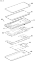
- the FPCB antenna module 501, the shielding member 502, the radiating sheet 503, the bonding member 504, and the printed circuit board 440 may be stacked in the internal space of the housing 401.
- the FPCB antenna module 501 may include an antenna pattern 511 and a nonconductive layer 512 surrounding the antenna pattern 511.
- the near-field communication pattern 511b may be disposed along the periphery of the wireless charging pattern 511a.
- the near-field communication pattern 511b may be patterned on both sides or one side of a base layer.
- the near-field communication pattern 511b may be electrically connected to the printed circuit board.
- the electronic device 400 may transmit and receive a signal to and from an external electronic device through the near-field communication pattern 511b.
- the antenna pattern 511 When an electric current flows through the antenna pattern 511 according to an antenna operation, heat may be generated due to resistance. When the generated heat is not properly radiated, the heat may accumulate in the electronic device 400, thus causing a deterioration in performance. Further, when the housing (e.g., a second side 310B of FIG. 3B ) of the electronic device 400 is heated by the heat generated by the antenna pattern 511, the user may experience discomfort when using the electronic device 400. To discharge the heat generated in the antenna pattern 511, the radiating sheet 503 may be attached to the antenna pattern 511.
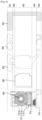
- the nonconductive layer 512 may extend from a third region 523 corresponding to the antenna pattern 511 to a first region 521 and a fifth region 525 in which an electronic component is disposed.
- An extended portion of the nonconductive layer 512 may be disposed to overlap the radiating sheet 503 and/or the electronic component.
- the extended portion of the nonconductive layer 512 may be attached to a portion of the electronic component through the bonding member 504.
- the FPCB antenna module 501 may include an additional conductive pattern 513.
- the FPCB antenna module 501 may include the additional conductive pattern 513 in a portion extending to the first region 521 or the fifth region 525.
- the additional conductive pattern 513 may be disposed in first, second, fourth, and fifth regions 521, 522, 524, and 525 of the FPCB antenna module 501.
- the additional conductive pattern 513 may be disposed along the outer boundary of the radiating sheet 503.
- the additional conductive pattern 513 may not function as a conducting wire. In another embodiment, the additional conductive pattern 513 may be electrically connected to the printed circuit board 440.
- the shielding member 502 may be attached to one side of the antenna pattern 511.
- the battery 450, the printed circuit board 440, or the support member 360 may be disposed on one surface of the shielding member 502, and the wireless charging pattern 511a, the near-field communication pattern 511b, or the magnetic secure transmission pattern 511c may be disposed on the other surface of the shielding member 502.
- the shielding member 502 may be formed of a material having a high permeability and a low loss tangent in the band of the near-field communication pattern 511b and the wireless charging pattern 511a.
- the shielding member 502 may include a microcrystalline material and may have a high permeability and a low loss tangent in the band of the near-field communication pattern 511b and the wireless charging pattern 511a of about 10 kHz to 15 MHz. Therefore, the shielding member 502 may be used as a ferromagnetic body in the band of the near-field communication pattern 511b and the wireless charging pattern 511a of about 10 kHz to 15 MHz.
- the printed circuit board 440 may extend from the first region 521 to the fifth region 525 along one edge of the housing 401.
- the electronic component on the printed circuit board 440 may be attached to or may be in contact with one surface of the radiating sheet 503 and/or the FPCB antenna module 501.
- a portion of the radiating sheet 503 may be attached to one surface of the shielding member 502. In certain embodiments, a portion of the radiating sheet 503 may be attached to a portion of the FPCB antenna module 501. In certain embodiments, a portion of the radiating sheet 503 may be attached to a portion of the electronic component. According to certain embodiments, the radiating sheet 503 may extend from the third region 523, where the antenna pattern 511 is disposed, to the first region 521 and/or the fifth region 525, where the electronic device 505 is disposed.
- the radiating sheet 503 is formed of one layer but is not limited thereto. In another embodiment, the radiating sheet 503 may be formed of a plurality of layers. The plurality of layers forming the radiating sheet 503 may have the same thickness, or at least one of the plurality of layers may have a different thickness.
- the bonding member 504 may be disposed between the radiating sheet 503 and the electronic component on the printed circuit board 440. In another embodiment, a portion of the bonding member 504 may be disposed between the FPCB antenna module 501 and the printed circuit board 440, and another portion thereof may be disposed between the printed circuit board 440 and the radiating sheet 503. In still another embodiment, the bonding member 504 may be disposed between the radiating sheet 503 (or the FPCB antenna module 501) and a structure inside the housing 401. Due to the bonding member 504, the FPCB antenna module 501 may be fixed in the housing, thus preventing the FPCB antenna module 501 from moving in the housing.
- the FPCB antenna module 501 may include the nonconductive layer 512 and the antenna pattern 511.
- the antenna pattern 511 and/or the nonconductive layer 512 may be formed of a plurality of layers.
- the antenna pattern 511 may include two layers.
- the FPCB antenna module 501 may extend from the region 523 in which the antenna pattern 511 is disposed to the region 521 in which the electronic component 505, which is an additional heat-generating source, is disposed or to a portion of the region 521.
- the extended portion may include only the nonconductive layer 512 without a conductive pattern (e.g., the antenna pattern 511).
- the shielding member 502 may be disposed on one surface of the FPCB antenna module 501. In certain embodiments, the shielding member 502 may be disposed to overlap the antenna pattern 511 of the FPCB antenna module 501. For example, the shielding member 502 may be attached to a region in which the wireless charging pattern 511a, the near-field communication pattern 511b, and the magnetic secure transmission pattern 511c of the FPCB antenna module 501are positioned.
- the radiating sheet 503 may be disposed in the third region 523, the fourth region 524, and the fifth region 525.
- a portion of the radiating sheet 503 may be attached to the FPCB antenna module 501 and another portion thereof may be attached to the electronic component 505.
- the radiating sheet 503 may be attached to a portion of the electronic component 505.
- the radiating sheet 503 may be disposed across the third to fifth regions 523, 524, and 525, thereby improving the heat radiation performance of the electronic device 400.
- the heat generated by the antenna pattern 511 in the third region 523 may spread not only in the radiating sheet 503 in the third region 523 but also to the radiating sheet in the fourth region 524 and the fifth region 525, thereby being relatively quickly radiated.
- the heat generated by the electronic component 505 in the fifth region 525 may spread not only in the radiating sheet 503 in the fifth region 525 but also to the radiating sheet 503 in the third region 523 and the fourth region 524, thereby being relatively quickly radiated.
- the bonding member 504 may be disposed between the radiating sheet 503 and the electronic component 505.
- the bonding member 504 may fix the FPCB antenna module 501 attached to the radiating sheet 503 in the housing.
- the bonding member 504 may be disposed between the extended FPCB antenna module 501 and the electronic component 505.
- the nonconductive layer 512 when the nonconductive layer 512 extends to the fifth region 525, the nonconductive layer 512 may withstand, along with the radiating sheet 503, stress due to a relative movement between the third region 523 and the fifth region 525.
- the FPCB antenna module 501 may further include an additional conductive pattern 513 in the extended portion. Referring to the non-limiting example of FIG. 11 , the portion of the radiating sheet 503 in the fifth region 525 may be surrounded by the additional conductive pattern 513.
- the nonconductive layer 512 and the further included additional conductive pattern 513 may withstand, along with the radiating sheet 503, stress due to the relative movement between the third region 523 and the fifth region 525. Therefore, damage to the radiating sheet 503 due to a relative movement occurring between the FPCB antenna module 501 and the electronic component 505 may be prevented.
- the FPCB antenna module 501 may include the nonconductive layer 512, the antenna pattern 511, and the additional conductive pattern 513.
- the nonconductive layer 512 of the FPCB antenna module 501 may extend from the third region 523, in which the antenna pattern 511 is formed, to the fifth region 525, in which the electronic component 505, which is an additional heat-generating source, is disposed, or to a portion of the fifth region 525.
- the FPCB antenna module 501 may include the additional conductive pattern 513 in the extended portion.
- the additional conductive pattern 513 may be electrically disconnected from the antenna pattern 511 disposed in the third region.
- the additional conductive pattern 513 may be electrically connected to the printed circuit board 440 so as to function as an electronic component (e.g., an antenna).
- the additional conductive pattern 513 may be disposed at a distance from the radiating sheet 503.
- the additional conductive pattern 513 may be spaced apart from an outer boundary of the radiating sheet 503.
- FIG. 9 illustrates, in cross-sectional view the example FPCB antenna module 501 taken along line C-C' in FIG. 5 .
- the FPCB antenna module 501 may include the nonconductive layer 512, the antenna pattern 511, and the additional conductive pattern 513. In certain embodiments, the FPCB antenna module 501 may extend from the region 523 in which the antenna pattern 511 is formed to the region 525 in which the electronic component 505, which is an additional heat-generating source, is disposed or to a portion of the region 525.
- the FPCB antenna module 501 may include the additional conductive pattern 513 in portions extending to the fourth region 524 and the fifth region 525.
- the additional conductive pattern 513 may be electrically disconnected (d2) from the antenna pattern 511.
- the radiating sheet 503 may be disposed to overlap the FPCB antenna module 501.
- the radiating sheet 503 may be disposed under the shielding member 502 and may receive heat from the FPCB antenna module 501 through the shielding member.
- the radiating sheet 503 may spread the received heat into the radiating sheet 503, thereby preventing the heat from accumulating in the FPCB antenna module 501.
- the bonding member 504 may be disposed between the FPCB antenna module 501 and the electronic component 505.
- the FPCB antenna module 501 is attached to the electronic component 505 in the illustrated embodiment, the embodiment is not limited thereto.
- the FPCB antenna module 501 may be attached to an apparatus inside the housing.
- the bonding member 504 may fix the FPCB antenna module 501 in the housing. By fixing the FPCB antenna module 501 in the housing, the FPCB antenna module 501 may be prevented from moving in the housing, and thus the FPCB antenna module 501 may operate normally.
- FIG. 10 illustrates, incross-sectional view, the example FPCB antenna module 501 taken along line D-D' in FIG. 5 .
- the non-limiting example of FIG. 10 shows a cross section of the FPCB antenna module 501 extending from the third region 523 to the fifth region 525, taken in a direction perpendicular to the extending direction.
- the additional conductive pattern 513 may be disposed in a portion of the nonconductive layer 512. According to certain embodiments, the additional conductive pattern 513 may be disposed at a distance from the radiating sheet 503. In certain embodiments, when the FPCB antenna module 501 is viewed from above, the radiating sheet 503 and the additional conductive pattern 513 may not overlap. For example, the radiating sheet 503 may be disposed under a portion 527 of the FPCB antenna module 501 including only the nonconductive layer 512. In certain embodiments, the electronic component 505 may be attached to a portion 526 including the additional conductive pattern 513 through the bonding member 504.
- the thickness of a component in which the radiating sheet 503 and the FPCB antenna module 501 are combined may be kept relatively constant. By reducing the thickness of the component in which the radiating sheet 503 and the FPCB antenna module 501 are combined, the internal space of the housing 500 may be efficiently used.
- the radiating sheet 503 is direct in contact with the electronic component 505 without the bonding member 504, the radiating sheet 503 may be less likely to be damaged when the FPCB antenna module 501 is separated from the electronic component 505.
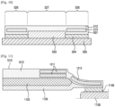
- FIG. 11 illustrates an example of a modified stacked structure of an FPCB antenna according to certain embodiments.
- FIG. 11 illustrates certain embodiments in which an additional conductive pattern is disposed to overlap a radiating sheet.
- the FPCB antenna module 1210 may include a nonconductive layer 1212, an antenna pattern 1211, and an additional conductive pattern 1213. In certain embodiments, the FPCB antenna module 1210 may extend from a region in which the conductive pattern 12111 is formed to a region in which an electronic component 1150, which is an additional heat-generating source, is disposed.
- a shielding member 1120 may be disposed on one surface of the FPCB antenna module 1210.
- the shielding member 1120 may be attached to a region corresponding to the conductive pattern 1111 of the FPCB antenna module 1210.
- a portion of a radiating sheet 1130 may be attached to the FPCB antenna module 12110, and another portion thereof may be attached to the electronic component 1150.
- the radiating sheet 1130 may extend from the region in which the conductive pattern 1211 of the FPCB antenna module 1210 is disposed to the region in which the electronic component 1150 is disposed.
- the heat radiation performance of the radiating sheet 1130 may be improved.
- the heat generated by the antenna pattern 1211 may spread not only in the radiating sheet 1130 in the region corresponding to the antenna pattern 1211 but also to the radiating sheet 1130 in the region in which the electronic component 1150 is disposed, thereby being relatively quickly radiated.
- a bonding member 1140 may be disposed between the radiating sheet 1130 and the electronic component 1150.
- the bonding member 1140 may fix the FPCB antenna module 1210 disposed on the radiating sheet 1130 in a housing. By fixing the FPCB antenna module 1210 in the housing, the FPCB antenna module 1210 may be prevented from moving in the housing.
- the nonconductive layer 1212 of the FPCB antenna module 1210 may extend to the region in which the electronic component 1150 is disposed.
- the FPCB antenna module 1210 may further include the additional conductive pattern 1213 in the extended portion.
- the additional conductive pattern 1213 may overlap the radiating sheet 1130.
- the FPCB antenna module 1110 including the nonconductive layer 1212 and the additional conductive pattern 1213 may withstand, along with the radiating sheet 1130, stress caused by a relative movement between the FPCB antenna module 1210 and the electronic component 1150.
Landscapes
- Engineering & Computer Science (AREA)
- Microelectronics & Electronic Packaging (AREA)
- Computer Networks & Wireless Communication (AREA)
- Signal Processing (AREA)
- Physics & Mathematics (AREA)
- Electromagnetism (AREA)
- Computer Hardware Design (AREA)
- Theoretical Computer Science (AREA)
- Manufacturing & Machinery (AREA)
- Human Computer Interaction (AREA)
- General Physics & Mathematics (AREA)
- General Engineering & Computer Science (AREA)
- Power Engineering (AREA)
- Telephone Function (AREA)
- Telephone Set Structure (AREA)
Description
- Certain embodiments according to the present disclosure relate to an electronic device including an extended flexible printed circuit board (FPCB) antenna module.
- A flexible printed circuit board (FPCB) is a thin and lightweight board that can fit into small spaces and be formed into specific shapes. An FPCB includes a conductive strip, such as a copper strip, and a nonconductive material, such as polyimide, surrounding the conductive strip. An FPCB is an electronic component for overcoming the weaknesses of an existing printed circuit board (PCB) in order to satisfy the trend toward compact and complex electronic products.
- As the performance of electronic products improves and the size thereof is decreased, electronic components mounted therein require high performance and are highly integrated, thus generating great heat in the electronic products. The generated heat reduces the lifespan of the products, causes malfunctions, or entails the risk of an explosion or fire. Therefore, a system for dissipating the heat generated inside the products to the outside or a self-cooling system is needed. A radiating sheet is generally used for electronic products requiring light weight and slimness.
-
US 20180026326 A1 discloses a heat dissipation sheet-integrated antenna module that is provided integrally with a heat dissipation sheet for dissipating heat generated in a portable device.US 20180205131 A1 discloses a portable terminal comprising a heat dissipating sheet having an antenna function to improve heat dissipation performance.US 2018/035528 A1 discloses a light weighted heat dissipation structure andUS 2018/301790 A1 discloses an electronic device including multiple coils. - The above information is presented as background information only to assist with an understanding of the disclosure. No determination has been made, and no assertion is made, as to whether any of the above might be applicable as prior art with regard to the disclosure.
- In certain embodiments according to this disclosure, electronic components are disposed in a housing of an electronic device. When the electronic device operates, heat may be generated in the electronic components (e.g., a wireless charging antenna, a processor, a speaker, and the like). To quickly discharge the heat, a radiating sheet may be attached to the electronic components. When a plurality of electronic components generating heat is attached to one radiating sheet, the radiating sheet may be damaged by a relative movement between the plurality of electronic components. When the radiating sheet is damaged, heat may accumulate in the electronic components, thus degrading the electronic components.
- The present invention is defined by appended set of claims. An electronic device is provided as defined in appended claims.
- An electronic device according to various embodiments includes a nonconductive layer extending on a radiating sheet to a region in which an electronic component is positioned, thereby enhancing the strength of the radiating sheet.
- Before undertaking the DETAILED DESCRIPTION below, it may be advantageous to set forth definitions of certain words and phrases used throughout this patent document: the terms "include" and "comprise," as well as derivatives thereof, mean inclusion without limitation; the term "or," is inclusive, meaning and/or; the phrases "associated with" and "associated therewith," as well as derivatives thereof, may mean to include, be included within, interconnect with, contain, be contained within, connect to or with, couple to or with, be communicable with, cooperate with, interleave, juxtapose, be proximate to, be bound to or with, have, have a property of, or the like; and the term "controller" means any device, system or part thereof that controls at least one operation, such a device may be implemented in hardware, firmware or software, or some combination of at least two of the same. It should be noted that the functionality associated with any particular controller may be centralized or distributed, whether locally or remotely.
- Moreover, various functions described below can be implemented or supported by one or more computer programs, each of which is formed from computer readable program code and embodied in a computer readable medium. The terms "application" and "program" refer to one or more computer programs, software components, sets of instructions, procedures, functions, objects, classes, instances, related data, or a portion thereof adapted for implementation in a suitable computer readable program code. The phrase "computer readable program code" includes any type of computer code, including source code, object code, and executable code. The phrase "computer readable medium" includes any type of medium capable of being accessed by a computer, such as read only memory (ROM), random access memory (RAM), a hard disk drive, a compact disc (CD), a digital video disc (DVD), or any other type of memory. A "non-transitory" computer readable medium excludes wired, wireless, optical, or other communication links that transport transitory electrical or other signals. A non-transitory computer readable medium includes media where data can be permanently stored and media where data can be stored and later overwritten, such as a rewritable optical disc or an erasable memory device.
- Definitions for certain words and phrases are provided throughout this patent document, those of ordinary skill in the art should understand that in many, if not most instances, such definitions apply to prior, as well as future uses of such defined words and phrases.
- For a more complete understanding of the present disclosure and its advantages, reference is now made to the following description taken in conjunction with the accompanying drawings, in which like reference numerals represent like parts:
-
FIG. 1 illustrates, in block diagram format, an electronic device in a network environment according to various embodiments of this disclosure; -
FIG. 2 illustrates, in block diagram format, a wireless communication module, a power management module, and an antenna module of an electronic device according to some embodiments of this disclosure; -
FIG. 3A illustrates, in perspective view, an example of an electronic device according to certain embodiments; -
FIG. 3B illustrates, in perspective view, the example electronic device ofFIG. 3A , as viewed from the back; -
FIG. 4 illustrates, in exploded perspective view, the example electronic device ofFIG. 3A ; -
FIG. 5 illustrates an example of the structure of an FPCB antenna module according to various embodiments of this disclosure; -
FIG. 6 illustrates, in exploded view layers forming the FPCB antenna module ofFIG. 5 ; -
FIG. 7 illustrates the FPCB antenna of the example ofFIG. 5 along a cross-sectional view taken along line A-A' inFIG. 5 ; -
FIG. 8 illustrates the FPCB antenna of the example ofFIG. 5 along a cross-sectional view taken along line B-B' inFIG. 5 ; -
FIG. 9 illustrates the FPCB antenna of the example ofFIG. 5 along a cross-sectional view taken along line C-C' inFIG. 5 ; -
FIG. 10 illustrates the FPCB antenna of the example ofFIG. 5 along a cross-sectional view taken along line D-D' inFIG. 5 ; and -
FIG. 11 illustrates an example of a modified stacked structure of an FPCB antenna according to certain embodiments of this disclosure. -
FIGS. 1 through 11 , discussed below, and the various embodiments used to describe the principles of the present disclosure in this patent document are by way of illustration only and should not be construed in any way to limit the scope of the disclosure. Those skilled in the art will understand that the principles of the present disclosure may be implemented in any suitably arranged system or device. -
FIG. 1 illustrates, in block diagram format, an example of anelectronic device 101 in anetwork environment 100 according to various embodiments. Referring to the non-limiting example ofFig. 1 , theelectronic device 101 in thenetwork environment 100 may communicate with anelectronic device 102 via a first network 198 (e.g., a short-range wireless communication network), or anelectronic device 104 or aserver 108 via a second network 199 (e.g., a long-range wireless communication network). According to certain embodiments, theelectronic device 101 may communicate with theelectronic device 104 via theserver 108. According to certain embodiments, theelectronic device 101 may include aprocessor 120,memory 130, aninput device 150, asound output device 155, adisplay device 160, anaudio module 170, asensor module 176, aninterface 177, ahaptic module 179, acamera module 180, apower management module 188, abattery 189, acommunication module 190, a subscriber identification module(SIM) 196, or anantenna module 197. In some embodiments, at least one (e.g., thedisplay device 160 or the camera module 180) of the components may be omitted from theelectronic device 101, or one or more other components may be added in theelectronic device 101. In some embodiments, some of the components may be implemented as single integrated circuitry. For example, the sensor module 176 (e.g., a fingerprint sensor, an iris sensor, or an illuminance sensor) may be implemented as embedded in the display device 160 (e.g., a display). - The
processor 120 may execute, for example, software (e.g., a program 140) to control at least one other component (e.g., a hardware or software component) of theelectronic device 101 coupled with theprocessor 120, and may perform various data processing or computation. According to one embodiment, as at least part of the data processing or computation, theprocessor 120 may load a command or data received from another component (e.g., thesensor module 176 or the communication module 190) involatile memory 132, process the command or the data stored in thevolatile memory 132, and store resulting data innon-volatile memory 134. According to certain embodiments, theprocessor 120 may include a main processor 121 (e.g., a central processing unit (CPU) or an application processor (AP)), and an auxiliary processor 123 (e.g., a graphics processing unit (GPU), an image signal processor (ISP), a sensor hub processor, or a communication processor (CP)) that is operable independently from, or in conjunction with, themain processor 121. Additionally or alternatively, theauxiliary processor 123 may be adapted to consume less power than themain processor 121, or to be specific to a specified function. Theauxiliary processor 123 may be implemented as separate from, or as part of themain processor 121. - The
auxiliary processor 123 may control at least some of functions or states related to at least one component (e.g., thedisplay device 160, thesensor module 176, or the communication module 190) among the components of theelectronic device 101, instead of themain processor 121 while themain processor 121 is in an inactive (e.g., sleep) state, or together with themain processor 121 while themain processor 121 is in an active state (e.g., executing an application). According to certain embodiments, the auxiliary processor 123 (e.g., an image signal processor or a communication processor) may be implemented as part of another component (e.g., thecamera module 180 or the communication module 190) functionally related to theauxiliary processor 123. - The
memory 130 may store various data used by at least one component (e.g., theprocessor 120 or the sensor module 176) of theelectronic device 101. The various data may include, for example, software (e.g., the program 140) and input data or output data for a command related thereto. Thememory 130 may include thevolatile memory 132 or thenon-volatile memory 134. - The
program 140 may be stored in thememory 130 as software, and may include, for example, an operating system (OS) 142,middleware 144, or anapplication 146. - The
input device 150 may receive a command or data to be used by other component (e.g., the processor 120) of theelectronic device 101, from the outside (e.g., a user) of theelectronic device 101. Theinput device 150 may include, for example, a microphone, a mouse, a keyboard, or a digital pen (e.g., a stylus pen). - The
sound output device 155 may output sound signals to the outside of theelectronic device 101. Thesound output device 155 may include, for example, a speaker or a receiver. The speaker may be used for general purposes, such as playing multimedia or playing record, and the receiver may be used for an incoming calls. According to certain embodiments, the receiver may be implemented as separate from, or as part of the speaker. - The
display device 160 may visually provide information to the outside (e.g., a user) of theelectronic device 101. Thedisplay device 160 may include, for example, a display, a hologram device, or a projector and control circuitry to control a corresponding one of the display, hologram device, and projector. According to certain embodiments, thedisplay device 160 may include touch circuitry adapted to detect a touch, or sensor circuitry (e.g., a pressure sensor) adapted to measure the intensity of force incurred by the touch. - The
audio module 170 may convert a sound into an electrical signal and vice versa. According to certain embodiments, theaudio module 170 may obtain the sound via theinput device 150, or output the sound via thesound output device 155 or a headphone of an external electronic device (e.g., an electronic device 102) directly (e.g., through a physical coupling, such as a wire) or wirelessly coupled with theelectronic device 101. - The
sensor module 176 may detect an operational state (e.g., power or temperature) of theelectronic device 101 or an environmental state (e.g., a state of a user) external to theelectronic device 101, and then generate an electrical signal or data value corresponding to the detected state. According to certain embodiments, thesensor module 176 may include, for example, a gesture sensor, a gyro sensor, an atmospheric pressure sensor, a magnetic sensor, an acceleration sensor, a grip sensor, a proximity sensor, a color sensor, an infrared (IR) sensor, a biometric sensor, a temperature sensor, a humidity sensor, or an illuminance sensor. - The
interface 177 may support one or more specified protocols to be used for theelectronic device 101 to be coupled with the external electronic device (e.g., the electronic device 102) directly (e.g., through a physical coupling, such as a wire) or wirelessly. According to certain embodiments, theinterface 177 may include, for example, a high definition multimedia interface (HDMI), a universal serial bus (USB) interface, a secure digital (SD) card interface, or an audio interface. - A connecting
terminal 178 may include a connector via which theelectronic device 101 may be physically connected with the external electronic device (e.g., the electronic device 102). According to certain embodiments, the connectingterminal 178 may include, for example, a HDMI connector, a USB connector, a SD card connector, or an audio connector (e.g., a headphone connector). - The
haptic module 179 may convert an electrical signal into a mechanical stimulus (e.g., a vibration or a movement) or electrical stimulus which may be recognized by a user via his tactile sensation or kinesthetic sensation. According to certain embodiments, thehaptic module 179 may include, for example, a motor, a piezoelectric element, or an electric stimulator. - The
camera module 180 may capture a still image or moving images. According to certain embodiments, thecamera module 180 may include one or more lenses, image sensors, image signal processors, or flashes. - The
power management module 188 may manage power supplied to theelectronic device 101. According to one embodiment, thepower management module 188 may be implemented as at least part of, for example, a power management integrated circuit (PMIC). - The
battery 189 may supply power to at least one component of theelectronic device 101. According to certain embodiments, thebattery 189 may include, for example, a primary cell which is not rechargeable, a secondary cell which is rechargeable, or a fuel cell. - The
communication module 190 may support establishing a direct (e.g., wired) communication channel or a wireless communication channel between theelectronic device 101 and the external electronic device (e.g., theelectronic device 102, theelectronic device 104, or the server 108) and performing communication via the established communication channel. Thecommunication module 190 may include one or more communication processors that are operable independently from the processor 120 (e.g., the application processor (AP)) and supports a direct (e.g., wired) communication or a wireless communication. According to certain embodiments, thecommunication module 190 may include a wireless communication module 192 (e.g., a cellular communication module, a short-range wireless communication module, or a global navigation satellite system (GNSS) communication module) or a wired communication module 194 (e.g., a local area network (LAN) communication module or a power line communication (PLC) module). A corresponding one of these communication modules may communicate with the external electronic device via the first network 198 (e.g., a short-range communication network, such as BLUETOOTH™, wireless-fidelity (WI-FI) direct, or infrared data association (IrDA)) or the second network 199 (e.g., a long-range communication network, such as a cellular network, the Internet, or a computer network (e.g., LAN or wide area network (WAN)). These various types of communication modules may be implemented as a single component (e.g., a single chip), or may be implemented as multi components (e.g., multi chips) separate from each other. Thewireless communication module 192 may identify and authenticate theelectronic device 101 in a communication network, such as thefirst network 198 or thesecond network 199, using subscriber information (e.g., international mobile subscriber identity (IMSI)) stored in thesubscriber identification module 196. - The
antenna module 197 may transmit or receive a signal or power to or from the outside (e.g., the external electronic device) of theelectronic device 101. According to certain embodiments, theantenna module 197 may include an antenna including a radiating element composed of a conductive material or a conductive pattern formed in or on a substrate (e.g., PCB). According to certain embodiments, theantenna module 197 may include a plurality of antennas. In such a case, at least one antenna appropriate for a communication scheme used in the communication network, such as thefirst network 198 or thesecond network 199, may be selected, for example, by the communication module 190 (e.g., the wireless communication module 192) from the plurality of antennas. The signal or the power may then be transmitted or received between thecommunication module 190 and the external electronic device via the selected at least one antenna. According to certain embodiments, another component (e.g., a radio frequency integrated circuit (RFIC)) other than the radiating element may be additionally formed as part of theantenna module 197. - At least some of the above-described components may be coupled mutually and communicate signals (e.g., commands or data) therebetween via an inter-peripheral communication scheme (e.g., a bus, general purpose input and output (GPIO), serial peripheral interface (SPI), or mobile industry processor interface (MIPI)).
- According to certain embodiments, commands or data may be transmitted or received between the
electronic device 101 and the externalelectronic device 104 via theserver 108 coupled with thesecond network 199. Each of theelectronic devices electronic device 101. According to certain embodiments, all or some of operations to be executed at theelectronic device 101 may be executed at one or more of the externalelectronic devices electronic device 101 should perform a function or a service automatically, or in response to a request from a user or another device, theelectronic device 101, instead of, or in addition to, executing the function or the service, may request the one or more external electronic devices to perform at least part of the function or the service. The one or more external electronic devices receiving the request may perform the at least part of the function or the service requested, or an additional function or an additional service related to the request, and transfer an outcome of the performing to theelectronic device 101. Theelectronic device 101 may provide the outcome, with or without further processing of the outcome, as at least part of a reply to the request. To that end, a cloud computing, distributed computing, or client-server computing technology may be used, for example. - The electronic device according to various embodiments may be one of various types of electronic devices. The electronic devices may include, for example, a portable communication device (e.g., a smartphone), a computer device, a portable multimedia device, a portable medical device, a camera, a wearable device, or a home appliance. According to certain embodiments of the disclosure, the electronic devices are not limited to those described above.
- With regard to the description of the drawings, similar reference numerals may be used to refer to similar or related elements. It is to be understood that a singular form of a noun corresponding to an item may include one or more of the things, unless the relevant context clearly indicates otherwise. As used herein, each of such phrases as "A or B," "at least one of A and B," "at least one of A or B," "A, B, or C," "at least one of A, B, and C," and "at least one of A, B, or C," may include any one of, or all possible combinations of the items enumerated together in a corresponding one of the phrases. As used herein, such terms as "1st" and "2nd," or "first" and "second" may be used to simply distinguish a corresponding component from another, and does not limit the components in other aspect (e.g., importance or order). It is to be understood that if an element (e.g., a first element) is referred to, with or without the term "operatively" or "communicatively", as "coupled with," "coupled to," "connected with," or "connected to" another element (e.g., a second element), it means that the element may be coupled with the other element directly (e.g., through a physical connection, such as a wire or bus), wirelessly, or via a third element.
- As used herein, the term "module" may include a unit implemented in hardware, software, or firmware, and may interchangeably be used with other terms, for example, "logic," "logic block," "part," or "circuitry". A module may be a single integral component, or a minimum unit or part thereof, adapted to perform one or more functions. For example, according to certain embodiments, the module may be implemented in a form of an application-specific integrated circuit (ASIC).
- Various embodiments as set forth herein may be implemented as software (e.g., the program 140) including one or more instructions that are stored in a storage medium (e.g.,
internal memory 136 or external memory 138) that is readable by a machine (e.g., the electronic device 101). For example, a processor(e.g., the processor 120) of the machine (e.g., the electronic device 101) may invoke at least one of the one or more instructions stored in the storage medium, and execute it, with or without using one or more other components under the control of the processor. This allows the machine to be operated to perform at least one function according to the at least one instruction invoked. The one or more instructions may include a code generated by a complier or a code executable by an interpreter. The machine-readable storage medium may be provided in the form of a non-transitory storage medium. Wherein, the term "non-transitory" simply means that the storage medium is a tangible device, and does not include a signal (e.g., an electromagnetic wave), but this term does not differentiate between where data is semi-permanently stored in the storage medium and where the data is temporarily stored in the storage medium. - According to certain embodiments, a method according to various embodiments of the disclosure may be included and provided in a computer program product. The computer program product may be traded as a product between a seller and a buyer. The computer program product may be distributed in the form of a machine-readable storage medium (e.g., compact disc read only memory (CD-ROM)), or be distributed (e.g., downloaded or uploaded) online via an application store (e.g., PLAYSTORE™), or between two user devices (e.g., smart phones) directly. If distributed online, at least part of the computer program product may be temporarily generated or at least temporarily stored in the machine-readable storage medium, such as memory of the manufacturer's server, a server of the application store, or a relay server.
- According to various embodiments, each component (e.g., a module or a program) of the above-described components may include a single entity or multiple entities. According to various embodiments, one or more of the above-described components may be omitted, or one or more other components may be added. Alternatively or additionally, a plurality of components (e.g., modules or programs) may be integrated into a single component. In such a case, according to various embodiments, the integrated component may still perform one or more functions of each of the plurality of components in the same or similar manner as they are performed by a corresponding one of the plurality of components before the integration. According to various embodiments, operations performed by the module, the program, or another component may be carried out sequentially, in parallel, repeatedly, or heuristically, or one or more of the operations may be executed in a different order or omitted, or one or more other operations may be added.
-
FIG. 2 illustrates, in a block diagram 200 , an example of thewireless communication module 192, thepower management module 188, and theantenna module 197 of theelectronic device 101 according to various embodiments. Referring to the non-limiting example ofFig. 2 , thewireless communication module 192 may include a magnetic secure transmission (MST)communication module 210 or a near-field communication (NFC) module 230, and thepower management module 188 may include awireless charging module 250. In such a case, theantenna module 197 may include a plurality of antennas that include a MST antenna 297-1 connected with theMST communication module 210, a NFC antenna 297-3 connected with the NFC communication module 230, and a wireless charging antenna 297-5 connected with thewireless charging module 250. For ease of description, the same components as those described in regard toFig. 1 are briefly described or omitted from the description. - The
MST communication module 210 may receive a signal containing control information or payment information such as card information from theprocessor 120, generate a magnetic signal corresponding to the received signal, and then transfer the generated magnetic signal to the external electronic device 102 (e.g., a point-of-sale (POS) device) via the MST antenna 297-1. To generate the magnetic signal, according to certain embodiments, theMST communication module 210 may include a switching module (not shown) that includes one or more switches connected with the MST antenna 297-1, and control the switching module to change the direction of voltage or current supplied to the MST antenna 297-1 according to the received signal. The change of the direction of the voltage or current allows the direction of the magnetic signal (e.g., a magnetic field) emitted from the MST antenna 297-1 to change accordingly. If detected at the externalelectronic device 102, the magnetic signal with its direction changing may cause an effect (e.g., a waveform) similar to that of a magnetic field that is generated when a magnetic card corresponding to the card information associated with the received signal is swiped through a card reader of theelectronic device 102. According to certain embodiments, for example, payment-related information and a control signal that are received by theelectronic device 102 in the form of the magnetic signal may be further transmitted to an external server 108 (e.g., a payment server) via thenetwork 199. - The NFC communication module 230 may obtain a signal containing control information or payment information such as card information from the
processor 120 and transmit the obtained signal to the externalelectronic device 102 via the NFC antenna 297-3. According to certain embodiments, the NFC communication module 230 may receive such a signal transmitted from the externalelectronic device 102 via the NFC antenna 297-3. - The
wireless charging module 250 may wirelessly transmit power to the external electronic device 102 (e.g., a cellular phone or wearable device) via the wireless charging antenna 297-5, or wirelessly receive power from the external electronic device 102 (e.g., a wireless charging device). Thewireless charging module 250 may support one or more of various wireless charging schemes including, for example, a magnetic resonance scheme or a magnetic induction scheme. - According to certain embodiments, some of the MST antenna 297-1, the NFC antenna 297-3, or the wireless charging antenna 297-5 may share at least part of their radiators. For example, the radiator of the MST antenna 297-1 may be used as the radiator of the NFC antenna 297-3 or the wireless charging antenna 297-5, or vice versa. In such a case, the
antenna module 197 may include a switching circuit (not shown) adapted to selectively connect (e.g., close) or disconnect (e.g. open) at least part of the antennas 297-1, 297-3, or 297-5, for example, under the control of the wireless communication module 192 (e.g., theMST communication module 210 or the NFC communication module 230) or the power management module (e.g., the wireless charging module 250). For example, when theelectronic device 101 uses a wireless charging function, the NFC communication module 230 or thewireless charging module 250 may control the switching circuit to temporarily disconnect at least one portion of the radiators shared by the NFC antenna 297-3 and the wireless charging antenna 297-5 from the NFC antenna 297-3 and to connect the at least one portion of the radiators with the wireless charging antenna 297-5. - According to certain embodiments, at least one function of the
MST communication module 210, the NFC communication module 230, or thewireless charging module 250 may be controlled by an external processor (e.g., the processor 120). According to certain embodiments, at least one specified function (e.g., a payment function) of theMST communication module 210 or the NFC communication module 230 may be performed in a trusted execution environment (TEE). According to certain embodiments, the TEE may form an execution environment in which, for example, at least some designated area of thememory 130 is allocated to be used for performing a function (e.g., a financial transaction or personal information-related function) that requires a relatively high level of security. In such a case, access to the at least some designated area of thememory 130 may be restrictively permitted, for example, according to an entity accessing thereto or an application being executed in the TEE. -
FIG. 3A illustrates, in perspective view, a front side of an example of mobileelectronic device 300 according to various embodiments of the present disclosure; -
FIG. 3B illustrates, in perspective view, a back side of the exampleelectronic device 300 ofFIG. 3A according to various embodiments of the present disclosure; - Referring to the non-limiting examples of
FIG. 3A andFIG. 3B , anelectronic device 300 according to certain embodiments may include ahousing 310 including a first side (or a front side) 310A, a second side (or a rear side) 310B, and a lateral side (surface) 310C surrounding a space between the first side 300A and thesecond side 310B. In certain embodiments, (not shown), the housing may refer to a structure which includes part of thefirst side 310A, second side 3 10B, andthird side 310C ofFIG. 1 . According to certain embodiments, the first side 110A may be constructed of a front plate 302 (or a front cover) (e.g., a polymer plate or a glass plate having various coating layers) which is at least partially transparent. - The second side 110B may be constructed of a rear plate 111 (or a rear cover) which may be opaque. For example, the rear plate 111 may be constructed, for example, and without limitation, of coated or colored glass, ceramic, polymer, metallic materials (e.g. aluminum, stainless steel (STS), or magnesium), a combination of at least two of these materials, or the like.
- The lateral side 110C (or a side member or side surface) may be constructed of a lateral bezel structure 118 (or a lateral member) bonded to the
front plate 302 and the rear plate 111 and including, for example, and without limitation, metal and/or polymer. In some embodiments, the rear plate 111 and the lateral bezel structure 118 may be constructed integrally and may include the same material (e.g., a metallic material such as aluminum). - According to certain embodiments, the
electronic device 300 may include at least one of adisplay 301, anaudio module camera module 305, akey input device 317, and aconnector hole 308. - In some embodiments, the
electronic device 300 may omit at least one of the components (for example, the key input device 317) or additionally include other components. For example, theelectronic device 300 may include a sensor module (not shown). For example, within an area provided by thefront plate 302, a sensor such as a proximity sensor or an illuminance sensor may be integrated into thedisplay 301, or may be disposed at a position adjacent to thedisplay 301. In some embodiments, theelectronic device 300 may further include a light-emitting device, and the light-emitting device may be disposed at a position adjacent to thedisplay 301 within an area provided by thefront plate 302. The light-emitting device may provide, for example, state information of theelectronic device 300 in the form of light. In another embodiment, the light-emitting device may provide, for example, a light source interlocked with the operation of thecamera module 305. The light-emitting element may include, for example, an LED, an IR LED, and a xenon lamp. - The
display 301 may be exposed, for example, through a significant portion of thefront plate 302. In some embodiments, the edge of thedisplay 301 may be formed to be substantially the same as an adjacent outer shape (e.g., a curved surface) of thefront plate 302. In another embodiment (not shown), in order to expand the area where thedisplay 301 is exposed, the distance between the outer edge of thedisplay 301 and the outer edge of thefront plate 302 may be substantially the same. In another embodiment (not shown), a recess or opening may be formed in a part of the screen display area of thedisplay 301, and the electronic device(300) may include another electronic components (e.g., acamera module 305, a proximity sensor or an illuminance sensor) aligned with the recess or the opening. - In another embodiment, at least one of the
camera modules fingerprint sensor 316, and theflash 306 may be included on the rear surface of the screen display area of thedisplay 301. In another embodiment, thedisplay 301 is coupled to or adjacent to a touch sensing circuit, a pressure sensor capable of measuring the intensity (pressure) of the touch, and/or a digitizer detecting a magnetic field type stylus pen. - The
audio modules - The
electronic device 300 may generate an electrical signal or data value corresponding to an internal operating state or an external environmental state by including a sensor module. The sensor module may include, for example, a proximity sensor disposed on thefirst surface 310A of thehousing 310, a fingerprint sensor integrated or adjacent to thedisplay 301, and/or a biometric sensor (e.g., an HRM sensor) disposed on thesecond surface 310B. Theelectronic device 300 includes a sensor module, for example, a gesture sensor, a gyro sensor, an air pressure sensor, a magnetic sensor, an acceleration sensor, a grip sensor, a color sensor, an infrared (IR) sensor, a biosensor, a temperature sensor, It may further include at least one of a humidity sensor or an illumination sensor. - The
camera modules first camera device 305 disposed on thefirst surface 310A of theelectronic device 300, asecond camera device flash 306 disposed on thesecond surface 310B. Thecamera devices flash 306 may include, for example, a light-emitting diode or a xenon lamp. In some embodiments, two or more lenses (infrared camera, wide-angle and telephoto lenses) and image sensors may be disposed on one side of theelectronic device 300. - The
key input device 317 may be disposed on theside 310C of thehousing 310. In other embodiments, theelectronic device 300 may not include some or all of the above-mentionedkey input devices 317, and thekey input devices 317 not included may be implemented in another form such as soft keys on thedisplay 301. In some embodiments, the key input device may include at least a portion of thefingerprint sensor 316. - The
connector hole 308 may accommodate a connector for transmitting and receiving power and/or data with an external electronic device, and/or a connector for transmitting and receiving audio signals with an external electronic device. For example, theconnector hole 308 may include a USB connector or an earphone jack. -
FIG. 4 illustrates the example electronic device ofFIG. 3A in an exploded perspective view. Referring to the non-limiting example ofFIG. 4 , theelectronic device 400 may include alateral bezel structure 410, a first support member 411 (e.g., a bracket), afront plate 420, adisplay 430, a printedcircuit board 440, abattery 450, a second support member 460 (e.g., a rear case), anantenna module 470, and arear plate 480. In some embodiments, at least one of the components (e.g., thefirst support member 411 or the second support member 460) may be omitted from theelectronic device 400, or a different component may be further included in theelectronic device 400. At least one of the components of theelectronic device 400 may be the same as or similar to at least one of the components of theelectronic device 300 ofFIG. 3A or3B , and a redundant description is omitted hereinafter. - According to various embodiments,
first support member 411 may be disposed in theelectronic device 400 and may be connected to thelateral bezel structure 410 or may be integrally formed with thelateral bezel structure 410. Thefirst support member 411 may be formed of, for example, a metallic material and/or a nonmetallic material (e.g., a polymer). Thefirst support member 411 may be coupled with thedisplay 430 on one surface thereof and may be coupled with the printedcircuit board 440 on the other surface thereof. A processor, a memory, and/or an interface may be mounted on the printedcircuit board 440. The processor may include, for example, one or more of a central processing unit, an application processor, a graphics processing unit, an image signal processor, a sensor hub processor, or a communication processor. - The memory may include, for example, a volatile memory or a nonvolatile memory.
- The interface may include, for example, a high-definition multimedia interface (HDMI), a universal serial bus (USB) interface, an SD card interface, and/or an audio interface. The interface may, for example, electrically or physically connect the
electronic device 400 to an external electronic device and may include a USB connector, an SD card/MMC connector, or an audio connector. - The
battery 450 is a device for supplying power to at least one component of theelectronic device 400 and may include, for example, a non-rechargeable primary cell, a rechargeable secondary cell, or a fuel cell. At least a portion of thebattery 450 may be disposed in substantially the same plane as, for example, the printedcircuit board 440. Thebattery 450 may be integrally disposed in theelectronic device 400 or may be detachably disposed in theelectronic device 400. - The
antenna module 470 may be disposed between therear plate 480 and thebattery 450. Theantenna module 470 may include, for example, a near-field communication (NFC) antenna, a wireless charging antenna, and/or a magnetic secure transmission (MST) antenna. Theantenna module 470 may, for example, perform short-range communication with an external device or may wirelessly transmit and receive power required for charging. In another embodiment, an antenna structure may be formed by thelateral bezel structure 410 and/or a portion of thefirst support member 411 or a combination thereof. -
FIG. 5 illustrates an example of a FPCB antenna module and layers attached to an FPCB antenna module according to certain embodiments.FIG. 6 illustrates, in an exploded view, an FPCB antenna module and layers attached to an FPCB antenna module according to certain embodiments. Referring to the non-limiting examples ofFIG. 5 andFIG. 6 , anelectronic device 400 according to certain embodiments may include a housing 401, anFPCB antenna module 501, a shieldingmember 502, aradiating sheet 503, abonding member 504, and a printedcircuit board 440. - According to certain embodiments, the housing 401 may form an internal space of the
electronic device 400. For example, the housing 401 may include alateral bezel structure 410 that forms a lateral side of theelectronic device 400. TheFPCB antenna module 501, the shieldingmember 502, the radiatingsheet 503, thebonding member 504, and the printedcircuit board 440 may be stacked in the internal space of the housing 401. - According to certain embodiments, the
FPCB antenna module 501 may include anantenna pattern 511 and anonconductive layer 512 surrounding theantenna pattern 511. - According to certain embodiments, the
antenna pattern 511 may include awireless charging pattern 511a, a near-field communication pattern 511b, and a magneticsecure transmission pattern 511c. Thewireless charging pattern 511a, the near-field communication pattern 511b, and the magneticsecure transmission pattern 511c may handle signals of different respective frequency bands. - According to certain embodiments, an electric current induced by an external charging device may be generated in the
wireless charging pattern 511a, and a battery (e.g., thebattery 450 ofFIG. 4 ) may be charged with the induced electric current. According to certain embodiments, the wireless charging pattern may be patterned with a conductive material on both sides of one base layer. According to certain embodiments, thewireless charging pattern 511a may be formed in concentric circles and may be electrically connected to the printed circuit board. - According to certain embodiments, the near-
field communication pattern 511b may be disposed along the periphery of thewireless charging pattern 511a. The near-field communication pattern 511b may be patterned on both sides or one side of a base layer. The near-field communication pattern 511b may be electrically connected to the printed circuit board. Theelectronic device 400 may transmit and receive a signal to and from an external electronic device through the near-field communication pattern 511b. - According to certain embodiments, the magnetic
secure transmission pattern 511c may be disposed in a region adjacent to thewireless charging pattern 511a. According to certain embodiments, the magneticsecure transmission pattern 511c may be formed to face one edge of the housing from thewireless charging pattern 511a. According to certain embodiments, the magneticsecure transmission pattern 511c may be electrically connected to the printed circuit board, and theelectronic device 400 may generate a specified magnetic field stored in a memory (e.g., thememory 130 ofFIG. 1 ) to transmit a signal to an external device through the magneticsecure transmission pattern 511c. - When an electric current flows through the
antenna pattern 511 according to an antenna operation, heat may be generated due to resistance. When the generated heat is not properly radiated, the heat may accumulate in theelectronic device 400, thus causing a deterioration in performance. Further, when the housing (e.g., asecond side 310B ofFIG. 3B ) of theelectronic device 400 is heated by the heat generated by theantenna pattern 511, the user may experience discomfort when using theelectronic device 400. To discharge the heat generated in theantenna pattern 511, the radiatingsheet 503 may be attached to theantenna pattern 511. - According to certain embodiments, the
nonconductive layer 512 may extend from athird region 523 corresponding to theantenna pattern 511 to afirst region 521 and afifth region 525 in which an electronic component is disposed. An extended portion of thenonconductive layer 512 may be disposed to overlap theradiating sheet 503 and/or the electronic component. The extended portion of thenonconductive layer 512 may be attached to a portion of the electronic component through thebonding member 504. - According to one embodiment, the
FPCB antenna module 501 may include an additionalconductive pattern 513. According to certain embodiments, theFPCB antenna module 501 may include the additionalconductive pattern 513 in a portion extending to thefirst region 521 or thefifth region 525. The additionalconductive pattern 513 may be disposed in first, second, fourth, andfifth regions FPCB antenna module 501. The additionalconductive pattern 513 may be disposed along the outer boundary of theradiating sheet 503. - In certain embodiments, the additional
conductive pattern 513 may not function as a conducting wire. In another embodiment, the additionalconductive pattern 513 may be electrically connected to the printedcircuit board 440. - In certain embodiments, the shielding
member 502 may be attached to one side of theantenna pattern 511. For example, thebattery 450, the printedcircuit board 440, or the support member 360 may be disposed on one surface of the shieldingmember 502, and thewireless charging pattern 511a, the near-field communication pattern 511b, or the magneticsecure transmission pattern 511c may be disposed on the other surface of the shieldingmember 502. - According to certain embodiments, the shielding
member 502 may minimize the impact of an electronic component on theantenna pattern 511. Further, the shieldingmember 502 may concentrate a magnetic field generated by theantenna pattern 511 on one side of the shieldingmember 502. For example, the shieldingmember 502 may concentrate the magnetic field generated in thewireless charging pattern 511a on a surface where a rear plate (e.g., therear plate 480 ofFIG. 4 ) of the housing is disposed, thereby increasing the charging efficiency of the battery. In another example, the shieldingmember 502 may concentrate the magnetic field generated in the near-field communication pattern 511b on the rear plate, thus enabling theelectronic device 400 to effectively perform near-field communication (NFC) with an external electronic device (e.g., theelectronic device 102 ofFIG. 1 ). - According to certain embodiments, a plurality of shielding
members 502 may be disposed to form layers. The shieldingmember 502 may have a different thickness depending on the position where the shieldingmember 502 is disposed and may be arranged in different forms. - In certain embodiments, the shielding
member 502 may be formed of a material having a high permeability and a low loss tangent in the band of the near-field communication pattern 511b and thewireless charging pattern 511a. The shieldingmember 502 may include a microcrystalline material and may have a high permeability and a low loss tangent in the band of the near-field communication pattern 511b and thewireless charging pattern 511a of about 10 kHz to 15 MHz. Therefore, the shieldingmember 502 may be used as a ferromagnetic body in the band of the near-field communication pattern 511b and thewireless charging pattern 511a of about 10 kHz to 15 MHz. - According to certain embodiments, an electronic component may be mounted or assembled on the printed
circuit board 440 disposed in a rear portion of the housing 401. The electronic component may include a processor (e.g., theprocessor 120 ofFIG. 1 ), a memory (e.g., thememory 130 ofFIG. 1 ), a display drive integrated (DDI) circuit, and a speaker module mounted on the printedcircuit board 440. - According to certain embodiments, the printed
circuit board 440 may extend from thefirst region 521 to thefifth region 525 along one edge of the housing 401. The electronic component on the printedcircuit board 440 may be attached to or may be in contact with one surface of theradiating sheet 503 and/or theFPCB antenna module 501. - According to certain embodiments, a portion of the
radiating sheet 503 may be attached to one surface of the shieldingmember 502. In certain embodiments, a portion of theradiating sheet 503 may be attached to a portion of theFPCB antenna module 501. In certain embodiments, a portion of theradiating sheet 503 may be attached to a portion of the electronic component. According to certain embodiments, the radiatingsheet 503 may extend from thethird region 523, where theantenna pattern 511 is disposed, to thefirst region 521 and/or thefifth region 525, where theelectronic device 505 is disposed. - In the illustrated embodiment, the radiating
sheet 503 is formed of one layer but is not limited thereto. In another embodiment, the radiatingsheet 503 may be formed of a plurality of layers. The plurality of layers forming theradiating sheet 503 may have the same thickness, or at least one of the plurality of layers may have a different thickness. - In certain embodiments, the radiating
sheet 503 may include graphite having excellent heat radiation performance in order to dissipate the heat generated in thewireless charging pattern 511a or the battery. - In certain embodiments, the
bonding member 504 may be disposed between the radiatingsheet 503 and the electronic component on the printedcircuit board 440. In another embodiment, a portion of thebonding member 504 may be disposed between theFPCB antenna module 501 and the printedcircuit board 440, and another portion thereof may be disposed between the printedcircuit board 440 and theradiating sheet 503. In still another embodiment, thebonding member 504 may be disposed between the radiating sheet 503 (or the FPCB antenna module 501) and a structure inside the housing 401. Due to thebonding member 504, theFPCB antenna module 501 may be fixed in the housing, thus preventing theFPCB antenna module 501 from moving in the housing. -
FIG. 7 illustrates, in cross-sectional view, the exampleFPCB antenna module 501 taken along line A-A' inFIG. 5 . - According to certain embodiments, a portion of the
radiating sheet 503 may be attached to the FPCB antenna module 501 (or the shieldingmember 502 attached to the FPCB antenna module 501), and another portion thereof may be attached to theelectronic component 505. According to the illustrated embodiment, the radiating sheet may be attached to the shieldingmember 502 in thethird region 523, may be attached to theFPCB antenna module 501 in thesecond region 522, and may be disposed between theFPCB antenna module 501 and theelectronic component 505 in thefirst region 521. In certain embodiments, thebonding member 504 may be disposed between the radiatingsheet 503 and theelectronic component 505. Thebonding member 504 may fix theFPCB antenna module 501 attached to theradiating sheet 503 in the housing. - The radiating
sheet 503 may be disposed across the threeregions electronic device 400. For example, the heat generated by theantenna pattern 511 in thethird region 523 may spread not only to theradiating sheet 503 in thethird region 523 but also to the radiating sheet in thefirst region 521 and thesecond region 522, thereby being radiated relatively quickly. In another example, the heat generated by theelectronic component 505 in thefirst region 521 may spread not only in theradiating sheet 503 in thefirst region 521 but also to theradiating sheet 503 in thesecond region 522 and thethird region 523, thereby being relatively quickly radiated. - According to certain embodiments, a relative movement may occur between the
FPCB antenna module 501 and theelectronic component 505 due to an external impact applied to theelectronic device 400. Due to this movement, stress may be concentrated on theradiating sheet 503 in thesecond region 522. In particular, when there is a step d1 in theradiating sheet 503 in thesecond region 522, the radiatingsheet 503 may be more vulnerable to the stress due to the relative movement that occurs between theFPCB antenna module 501 and theelectronic component 505, compared to the case where there is no step. - In certain embodiments, the
nonconductive layer 512 of theFPCB antenna module 501 may extend from thethird region 523 to thefirst region 521 through thesecond region 522. When thenonconductive layer 512 extends from thethird region 523 to thesecond region 522 and thefirst region 521, the extended portion of thenonconductive layer 512 may withstand, along with the radiatingsheet 503, the stress due to the relative movement between thefirst region 521 and thethird region 523. Therefore, damage to theradiating sheet 503 due to a relative movement occurring between theFPCB antenna module 501 and theelectronic component 505 may be prevented. - According to certain embodiments, the
FPCB antenna module 501 may include thenonconductive layer 512 and theantenna pattern 511. In certain embodiments, theantenna pattern 511 and/or thenonconductive layer 512 may be formed of a plurality of layers. For example, as illustrated in the embodiment, theantenna pattern 511 may include two layers. - According to certain embodiments, the
FPCB antenna module 501 may extend from theregion 523 in which theantenna pattern 511 is disposed to theregion 521 in which theelectronic component 505, which is an additional heat-generating source, is disposed or to a portion of theregion 521. In one embodiment, the extended portion may include only thenonconductive layer 512 without a conductive pattern (e.g., the antenna pattern 511). - According to certain embodiments, the shielding
member 502 may be disposed on one surface of theFPCB antenna module 501. In certain embodiments, the shieldingmember 502 may be disposed to overlap theantenna pattern 511 of theFPCB antenna module 501. For example, the shieldingmember 502 may be attached to a region in which thewireless charging pattern 511a, the near-field communication pattern 511b, and the magneticsecure transmission pattern 511c of the FPCB antenna module 501are positioned. -
FIG. 8 illustrates, in cross-sectional view the exampleFPCB antenna module 501 taken along line B-B' ofFIG. 5 . - According to certain embodiments, the radiating
sheet 503 may be disposed in thethird region 523, thefourth region 524, and thefifth region 525. For example, a portion of theradiating sheet 503 may be attached to theFPCB antenna module 501 and another portion thereof may be attached to theelectronic component 505. According to various embodiments, the radiatingsheet 503 may be attached to a portion of theelectronic component 505. - The radiating
sheet 503 may be disposed across the third tofifth regions electronic device 400. For example, the heat generated by theantenna pattern 511 in thethird region 523 may spread not only in theradiating sheet 503 in thethird region 523 but also to the radiating sheet in thefourth region 524 and thefifth region 525, thereby being relatively quickly radiated. In another example, the heat generated by theelectronic component 505 in thefifth region 525 may spread not only in theradiating sheet 503 in thefifth region 525 but also to theradiating sheet 503 in thethird region 523 and thefourth region 524, thereby being relatively quickly radiated. - According to certain embodiments, the
bonding member 504 may be disposed between the radiatingsheet 503 and theelectronic component 505. Thebonding member 504 may fix theFPCB antenna module 501 attached to theradiating sheet 503 in the housing. According to certain embodiments, thebonding member 504 may be disposed between the extendedFPCB antenna module 501 and theelectronic component 505. - In certain embodiments, when the
nonconductive layer 512 extends to thefifth region 525, thenonconductive layer 512 may withstand, along with the radiatingsheet 503, stress due to a relative movement between thethird region 523 and thefifth region 525. According to certain embodiments, theFPCB antenna module 501 may further include an additionalconductive pattern 513 in the extended portion. Referring to the non-limiting example ofFIG. 11 , the portion of theradiating sheet 503 in thefifth region 525 may be surrounded by the additionalconductive pattern 513. Thenonconductive layer 512 and the further included additionalconductive pattern 513 may withstand, along with the radiatingsheet 503, stress due to the relative movement between thethird region 523 and thefifth region 525. Therefore, damage to theradiating sheet 503 due to a relative movement occurring between theFPCB antenna module 501 and theelectronic component 505 may be prevented. - According to certain embodiments, the
FPCB antenna module 501 may include thenonconductive layer 512, theantenna pattern 511, and the additionalconductive pattern 513. - In certain embodiments, the
nonconductive layer 512 of theFPCB antenna module 501 may extend from thethird region 523, in which theantenna pattern 511 is formed, to thefifth region 525, in which theelectronic component 505, which is an additional heat-generating source, is disposed, or to a portion of thefifth region 525. - In certain embodiments, the
FPCB antenna module 501 may include the additionalconductive pattern 513 in the extended portion. In certain embodiments, the additionalconductive pattern 513 may be electrically disconnected from theantenna pattern 511 disposed in the third region. In another embodiment, the additionalconductive pattern 513 may be electrically connected to the printedcircuit board 440 so as to function as an electronic component (e.g., an antenna). - According to certain embodiments, the additional
conductive pattern 513 may be disposed at a distance from the radiatingsheet 503. For example, the additionalconductive pattern 513 may be spaced apart from an outer boundary of theradiating sheet 503. -
FIG. 9 illustrates, in cross-sectional view the exampleFPCB antenna module 501 taken along line C-C' inFIG. 5 . - According to certain embodiments, the
FPCB antenna module 501 may include thenonconductive layer 512, theantenna pattern 511, and the additionalconductive pattern 513. In certain embodiments, theFPCB antenna module 501 may extend from theregion 523 in which theantenna pattern 511 is formed to theregion 525 in which theelectronic component 505, which is an additional heat-generating source, is disposed or to a portion of theregion 525. - According to certain embodiments, the
FPCB antenna module 501 may include the additionalconductive pattern 513 in portions extending to thefourth region 524 and thefifth region 525. In certain embodiments, the additionalconductive pattern 513 may be electrically disconnected (d2) from theantenna pattern 511. - According to certain embodiments, the radiating
sheet 503 may be disposed to overlap theFPCB antenna module 501. The radiatingsheet 503 may be disposed under the shieldingmember 502 and may receive heat from theFPCB antenna module 501 through the shielding member. The radiatingsheet 503 may spread the received heat into theradiating sheet 503, thereby preventing the heat from accumulating in theFPCB antenna module 501. - According to certain embodiments, the
bonding member 504 may be disposed between theFPCB antenna module 501 and theelectronic component 505. Although theFPCB antenna module 501 is attached to theelectronic component 505 in the illustrated embodiment, the embodiment is not limited thereto. For example, theFPCB antenna module 501 may be attached to an apparatus inside the housing. Thebonding member 504 may fix theFPCB antenna module 501 in the housing. By fixing theFPCB antenna module 501 in the housing, theFPCB antenna module 501 may be prevented from moving in the housing, and thus theFPCB antenna module 501 may operate normally. -
FIG. 10 illustrates, incross-sectional view, the exampleFPCB antenna module 501 taken along line D-D' inFIG. 5 . The non-limiting example ofFIG. 10 shows a cross section of theFPCB antenna module 501 extending from thethird region 523 to thefifth region 525, taken in a direction perpendicular to the extending direction. - The additional
conductive pattern 513 may be disposed in a portion of thenonconductive layer 512. According to certain embodiments, the additionalconductive pattern 513 may be disposed at a distance from the radiatingsheet 503. In certain embodiments, when theFPCB antenna module 501 is viewed from above, the radiatingsheet 503 and the additionalconductive pattern 513 may not overlap. For example, the radiatingsheet 503 may be disposed under aportion 527 of theFPCB antenna module 501 including only thenonconductive layer 512. In certain embodiments, theelectronic component 505 may be attached to aportion 526 including the additionalconductive pattern 513 through thebonding member 504. - Since the additional
conductive pattern 513 is disposed at a distance from the radiatingsheet 503, the thickness of a component in which theradiating sheet 503 and theFPCB antenna module 501 are combined may be kept relatively constant. By reducing the thickness of the component in which theradiating sheet 503 and theFPCB antenna module 501 are combined, the internal space of the housing 500 may be efficiently used. - Further, since the
radiating sheet 503 is direct in contact with theelectronic component 505 without thebonding member 504, the radiatingsheet 503 may be less likely to be damaged when theFPCB antenna module 501 is separated from theelectronic component 505. -
FIG. 11 illustrates an example of a modified stacked structure of an FPCB antenna according to certain embodiments.FIG. 11 illustrates certain embodiments in which an additional conductive pattern is disposed to overlap a radiating sheet. - According to certain embodiments, the
FPCB antenna module 1210 may include anonconductive layer 1212, anantenna pattern 1211, and an additionalconductive pattern 1213. In certain embodiments, theFPCB antenna module 1210 may extend from a region in which the conductive pattern 12111 is formed to a region in which anelectronic component 1150, which is an additional heat-generating source, is disposed. - According to certain embodiments, a shielding
member 1120 may be disposed on one surface of theFPCB antenna module 1210. The shieldingmember 1120 may be attached to a region corresponding to the conductive pattern 1111 of theFPCB antenna module 1210. - According to certain embodiments, a portion of a
radiating sheet 1130 may be attached to the FPCB antenna module 12110, and another portion thereof may be attached to theelectronic component 1150. For example, theradiating sheet 1130 may extend from the region in which theconductive pattern 1211 of theFPCB antenna module 1210 is disposed to the region in which theelectronic component 1150 is disposed. - By extending the
radiating sheet 1130, the heat radiation performance of theradiating sheet 1130 may be improved. For example, the heat generated by theantenna pattern 1211 may spread not only in theradiating sheet 1130 in the region corresponding to theantenna pattern 1211 but also to theradiating sheet 1130 in the region in which theelectronic component 1150 is disposed, thereby being relatively quickly radiated. - According to certain embodiments, a
bonding member 1140 may be disposed between the radiatingsheet 1130 and theelectronic component 1150. Thebonding member 1140 may fix theFPCB antenna module 1210 disposed on theradiating sheet 1130 in a housing. By fixing theFPCB antenna module 1210 in the housing, theFPCB antenna module 1210 may be prevented from moving in the housing. - The
nonconductive layer 1212 of theFPCB antenna module 1210 may extend to the region in which theelectronic component 1150 is disposed. According to certain embodiments, theFPCB antenna module 1210 may further include the additionalconductive pattern 1213 in the extended portion. The additionalconductive pattern 1213 may overlap theradiating sheet 1130. The FPCB antenna module 1110 including thenonconductive layer 1212 and the additionalconductive pattern 1213 may withstand, along with theradiating sheet 1130, stress caused by a relative movement between theFPCB antenna module 1210 and theelectronic component 1150. - In the specific embodiments of this disclosure described above, the elements included in the invention have been represented singular or plural in accordance with the specific embodiments shown. It should be understood, however, that the singular or plural representations are selected appropriately according to the situations presented for the convenience of description, and the disclosure is not limited to the singular or plural constituent elements, and may be composed of a plurality of elements even if they are expressed.
- Although the present disclosure has been described with various embodiments, various changes and modifications may be suggested to one skilled in the art. It is intended that the present disclosure encompass such changes and modifications as fall within the scope of the appended claims.
Claims (15)
- An electronic device (400) comprising:a housing (401) configured to form an internal space;a radiating sheet (503) configured to be disposed in the internal space;at least one electronic component (505) configured to be disposed in the internal space and to be connected to the radiating sheet (503); anda flexible printed circuit board, FPCB, antenna module (501) configured to be disposed on the radiating sheet (503) and to comprise an antenna pattern (511) and a nonconductive layer (512), the nonconductive layer (512) being configured to surround the antenna pattern (511),wherein the nonconductive layer (512) extends to a region in which the electronic component (505) is positioned.
- The electronic device of claim 1, further comprising:
a shielding member (502) configured to be stacked between the radiating sheet (503) and the FPCB antenna module (501). - The electronic device of claim 1, further comprising:
a bonding member (504) configured to be disposed between the radiating sheet (503) and the electronic component (505). - The electronic device of claim 1, further comprising:
a bonding member (504) configured to be disposed between the FPCB antenna module (501) and the electronic component (505). - The electronic device of claim 1, wherein the FPCB antenna module (501) further comprises an additional conductive pattern (513) in a portion that extends to the electronic component (505).
- The electronic device of claim 5, wherein the additional conductive pattern (513) extends from a region adjacent to the antenna pattern (511) to the region in which the electronic component (505) is positioned.
- The electronic device of claim 5, wherein the additional conductive pattern (513) is electrically disconnected from the antenna pattern (511).
- The electronic device of claim 5, wherein the additional conductive pattern (513) is spaced apart from a boundary of the radiating sheet (503) when the FPCB antenna module (501) is viewed from above.
- The electronic device of claim 5, wherein the additional conductive pattern (513) is formed along a boundary of the portion of the FPCB antenna module (501) that extends to the electronic component (505).
- The electronic device of claim 1, wherein the antenna pattern (511) comprises an antenna that operates as at least one of a near-field communication, NFC, pattern or a magnetic secure transmission, MST, pattern.
- The electronic device of claim 1, wherein the FPCB antenna module (501) is disposed on a surface of the radiating sheet (503), and the electronic component (505) is disposed on a surface looking in a different direction from that of the surface of the radiating sheet (503).
- The electronic device of claim 1, wherein the electronic component (505) further comprises a portion of a printed circuit board, PCB, (440).
- The electronic device of claim 1, wherein the radiating sheet (503) comprises a step between a portion thereof attached to the antenna pattern (511) and a portion thereof attached to the electronic component (1150).
- The electronic device of claim 1, further comprising:
a bonding member (504) configured to be disposed between a structure in the housing (401) and an extended portion of the FPCB antenna module (501). - The electronic device of claim 1, wherein a portion of the electronic component (1150) is attached to the radiating sheet (503), and another portion thereof is attached to an extended portion of the FPCB antenna module (501).
Applications Claiming Priority (2)
| Application Number | Priority Date | Filing Date | Title |
|---|---|---|---|
| KR1020190035389A KR102613670B1 (en) | 2019-03-27 | 2019-03-27 | An electronic device including an expanded flexible print circuit board antenna module |
| PCT/KR2020/004273 WO2020197345A1 (en) | 2019-03-27 | 2020-03-27 | Electronic device including expanded flexible printed circuit board antenna module |
Publications (3)
| Publication Number | Publication Date |
|---|---|
| EP3903377A1 EP3903377A1 (en) | 2021-11-03 |
| EP3903377A4 EP3903377A4 (en) | 2022-03-02 |
| EP3903377B1 true EP3903377B1 (en) | 2024-07-03 |
Family
ID=72603673
Family Applications (1)
| Application Number | Title | Priority Date | Filing Date |
|---|---|---|---|
| EP20778501.5A Active EP3903377B1 (en) | 2019-03-27 | 2020-03-27 | Electronic device including expanded flexible printed circuit board antenna module |
Country Status (5)
| Country | Link |
|---|---|
| US (1) | US11431083B2 (en) |
| EP (1) | EP3903377B1 (en) |
| KR (1) | KR102613670B1 (en) |
| CN (1) | CN113632316B (en) |
| WO (1) | WO2020197345A1 (en) |
Families Citing this family (10)
| Publication number | Priority date | Publication date | Assignee | Title |
|---|---|---|---|---|
| KR20220017182A (en) * | 2020-08-04 | 2022-02-11 | 삼성전자주식회사 | AN APPARATUS COMPRISING FPCB(flexible printed circuit board) FOR SHIELDING ELECTROMAGNETIC INTERFERENCE |
| KR102847031B1 (en) * | 2020-12-21 | 2025-08-20 | 삼성전자주식회사 | Electronic device including coil antenna |
| KR102919981B1 (en) * | 2021-02-03 | 2026-01-30 | 삼성전자주식회사 | Flexible assembly including antenna pattern and electronic device with the same |
| BR112023020782A2 (en) | 2021-04-06 | 2023-12-12 | Samsung Electronics Co Ltd | ELECTRONIC DEVICE INCLUDING HEAT DISSIPATION STRUCTURE |
| KR102893336B1 (en) * | 2021-04-06 | 2025-12-01 | 삼성전자주식회사 | Electronic device including heat radiating structure |
| KR20230005630A (en) | 2021-07-01 | 2023-01-10 | 삼성전자주식회사 | An electronic device comprising an antenna |
| US11777218B2 (en) * | 2021-12-27 | 2023-10-03 | Google Llc | Antenna design with structurally integrated composite antenna components |
| US20230299165A1 (en) * | 2022-03-15 | 2023-09-21 | Intel Corporation | Fabrication of gate-all-around integrated circuit structures having pre-spacer-deposition wide cut gates with non-merged spacers |
| US20230352823A1 (en) * | 2022-04-28 | 2023-11-02 | Meta Platforms Technologies, Llc | Flexible printed circuit board with near-field communication (nfc) coil integration |
| EP4679626A1 (en) | 2023-07-10 | 2026-01-14 | Samsung Electronics Co., Ltd. | Electronic device comprising antenna module |
Family Cites Families (23)
| Publication number | Priority date | Publication date | Assignee | Title |
|---|---|---|---|---|
| JP5051189B2 (en) | 2009-07-10 | 2012-10-17 | アイシン・エィ・ダブリュ株式会社 | Electronic circuit equipment |
| KR101570617B1 (en) | 2014-09-05 | 2015-11-20 | 엘지디스플레이 주식회사 | Flexible printed circuit board and touch panel including the same |
| KR101643928B1 (en) * | 2014-11-26 | 2016-07-29 | (주)파트론 | Antenna structure |
| KR20160090144A (en) | 2015-01-21 | 2016-07-29 | 주식회사 아모그린텍 | Heat dissipation sheet unified antenna module |
| KR102294019B1 (en) * | 2015-01-28 | 2021-08-26 | 삼성전자주식회사 | Antenna and electronic device having it |
| KR102314790B1 (en) * | 2015-02-26 | 2021-10-20 | 삼성전자주식회사 | Electronic device including antenna device |
| CN204596965U (en) | 2015-05-12 | 2015-08-26 | 深圳市嘉姆特科技有限公司 | A kind of multi-functional NFC antenna |
| KR102342852B1 (en) | 2015-06-16 | 2021-12-23 | 삼성전자주식회사 | Wireless communication module and portable terminal including the same |
| KR101609642B1 (en) | 2015-07-10 | 2016-04-08 | 주식회사 아모그린텍 | Heat Radiation Unit with integrated Near Field Communication antenna and Portable device having the same |
| KR102487477B1 (en) | 2016-01-20 | 2023-01-12 | 삼성전자주식회사 | Antenna using Display |
| KR102567364B1 (en) * | 2016-01-27 | 2023-08-16 | 삼성전자주식회사 | Antenna Assist Device and Electronic device including the same |
| CN205622671U (en) * | 2016-03-18 | 2016-10-05 | 上海与德通讯技术有限公司 | Mobile terminal |
| KR102466002B1 (en) * | 2016-04-19 | 2022-11-11 | 삼성전자주식회사 | Electronic device including antenna |
| EP3236390B1 (en) * | 2016-04-19 | 2021-11-24 | Samsung Electronics Co., Ltd. | Electronic device supporting fingerprint verification and method for operating the same |
| KR102497472B1 (en) | 2016-07-29 | 2023-02-08 | 삼성전자주식회사 | Electronic device including waterproof structure |
| KR102483238B1 (en) | 2016-08-01 | 2022-12-30 | 삼성전자 주식회사 | Heat dissipation apparatus and electronic device having the same |
| KR102621757B1 (en) * | 2016-09-07 | 2024-01-08 | 삼성전자주식회사 | the Antenna for Wireless Communication and the Electronic Device including the same |
| CN109804501B (en) * | 2016-09-23 | 2021-04-30 | 阿莫技术有限公司 | Antenna module |
| KR102335846B1 (en) * | 2017-04-17 | 2021-12-07 | 삼성전자주식회사 | Electronic device comprising a plurality of coils |
| US10720695B2 (en) * | 2017-05-15 | 2020-07-21 | Speedlink Technology Inc. | Near field communication antenna modules for devices with metal frame |
| KR20190006343A (en) * | 2017-07-10 | 2019-01-18 | 송영석 | Structure of radiant heat wireless communications antenna |
| US10141625B1 (en) | 2017-07-13 | 2018-11-27 | Lg Electronics Inc. | Mobile terminal |
| KR102514547B1 (en) * | 2018-07-16 | 2023-03-27 | 삼성전자주식회사 | Display assembly including antenna and electronic device with the same |
-
2019
- 2019-03-27 KR KR1020190035389A patent/KR102613670B1/en active Active
-
2020
- 2020-03-27 US US16/833,170 patent/US11431083B2/en active Active
- 2020-03-27 CN CN202080024587.3A patent/CN113632316B/en active Active
- 2020-03-27 WO PCT/KR2020/004273 patent/WO2020197345A1/en not_active Ceased
- 2020-03-27 EP EP20778501.5A patent/EP3903377B1/en active Active
Also Published As
| Publication number | Publication date |
|---|---|
| EP3903377A4 (en) | 2022-03-02 |
| US11431083B2 (en) | 2022-08-30 |
| CN113632316B (en) | 2024-09-10 |
| KR20200114150A (en) | 2020-10-07 |
| WO2020197345A1 (en) | 2020-10-01 |
| KR102613670B1 (en) | 2023-12-14 |
| EP3903377A1 (en) | 2021-11-03 |
| US20200313284A1 (en) | 2020-10-01 |
| CN113632316A (en) | 2021-11-09 |
Similar Documents
| Publication | Publication Date | Title |
|---|---|---|
| US11431083B2 (en) | Electronic device including expanded flexible printed circuit board antenna module | |
| US11886238B2 (en) | Foldable electronic device | |
| KR102651418B1 (en) | Electronic device including a shielding sheet and a heat radiation member | |
| KR102659482B1 (en) | Electronic device including interposer | |
| US10854958B2 (en) | Electronic device including grip sensor and antenna | |
| US11019736B2 (en) | Electronic device including flexible printed circuit board | |
| US11665818B2 (en) | Electronic device including flexible printed circuit board laminated wireless charging coil and near field communication antenna pattern | |
| US10965157B2 (en) | Electronic device having a plurality of stacked coil antennas | |
| EP3794808B1 (en) | Electronic device including flexible printed circuit board adjacent to antenna | |
| US12395578B2 (en) | Electronic device comprising housing | |
| US11825007B2 (en) | Component stack mounting structure and electronic device including same | |
| US11258174B2 (en) | Antenna radiator including plurality of layers and electronic device including the same | |
| US12250798B2 (en) | Electronic device including heat dissipation sheet | |
| US20200127382A1 (en) | Electronic device including antenna apparatus using photo-conductive material and antenna control method | |
| EP4333568B1 (en) | Rigid flexible printed circuit board and electronic device comprising same | |
| KR102960119B1 (en) | Wireless charging coil and electronic device with the same | |
| US12272864B2 (en) | Electronic device including antenna | |
| US20240332797A1 (en) | Antenna structure and electronic device including same | |
| EP4629038A1 (en) | Display module including structure for reducing damage and electronic device comprising same | |
| EP4510380A1 (en) | Antenna and electronic device comprising antenna | |
| US20250338396A1 (en) | Electronic device comprising flexible printed circuit board | |
| KR20240145843A (en) | Antenna structure and electronic device including the same | |
| KR20230055245A (en) | Wireless charging coil and electronic device with the same |
Legal Events
| Date | Code | Title | Description |
|---|---|---|---|
| STAA | Information on the status of an ep patent application or granted ep patent |
Free format text: STATUS: THE INTERNATIONAL PUBLICATION HAS BEEN MADE |
|
| PUAI | Public reference made under article 153(3) epc to a published international application that has entered the european phase |
Free format text: ORIGINAL CODE: 0009012 |
|
| STAA | Information on the status of an ep patent application or granted ep patent |
Free format text: STATUS: REQUEST FOR EXAMINATION WAS MADE |
|
| 17P | Request for examination filed |
Effective date: 20210727 |
|
| AK | Designated contracting states |
Kind code of ref document: A1 Designated state(s): AL AT BE BG CH CY CZ DE DK EE ES FI FR GB GR HR HU IE IS IT LI LT LU LV MC MK MT NL NO PL PT RO RS SE SI SK SM TR |
|
| A4 | Supplementary search report drawn up and despatched |
Effective date: 20220131 |
|
| RIC1 | Information provided on ipc code assigned before grant |
Ipc: G06F 1/20 20060101ALI20220125BHEP Ipc: H01Q 1/24 20060101ALI20220125BHEP Ipc: H01Q 1/22 20060101ALI20220125BHEP Ipc: H01Q 1/02 20060101AFI20220125BHEP |
|
| DAV | Request for validation of the european patent (deleted) | ||
| DAX | Request for extension of the european patent (deleted) | ||
| GRAP | Despatch of communication of intention to grant a patent |
Free format text: ORIGINAL CODE: EPIDOSNIGR1 |
|
| STAA | Information on the status of an ep patent application or granted ep patent |
Free format text: STATUS: GRANT OF PATENT IS INTENDED |
|
| INTG | Intention to grant announced |
Effective date: 20240208 |
|
| RIN1 | Information on inventor provided before grant (corrected) |
Inventor name: KIM, HOJONG Inventor name: KEUM, KYEONGJO Inventor name: KIM, YOUNJU |
|
| GRAS | Grant fee paid |
Free format text: ORIGINAL CODE: EPIDOSNIGR3 |
|
| GRAA | (expected) grant |
Free format text: ORIGINAL CODE: 0009210 |
|
| STAA | Information on the status of an ep patent application or granted ep patent |
Free format text: STATUS: THE PATENT HAS BEEN GRANTED |
|
| AK | Designated contracting states |
Kind code of ref document: B1 Designated state(s): AL AT BE BG CH CY CZ DE DK EE ES FI FR GB GR HR HU IE IS IT LI LT LU LV MC MK MT NL NO PL PT RO RS SE SI SK SM TR |
|
| REG | Reference to a national code |
Ref country code: CH Ref legal event code: EP |
|
| REG | Reference to a national code |
Ref country code: DE Ref legal event code: R096 Ref document number: 602020033412 Country of ref document: DE |
|
| REG | Reference to a national code |
Ref country code: NL Ref legal event code: FP |
|
| REG | Reference to a national code |
Ref country code: LT Ref legal event code: MG9D |
|
| PG25 | Lapsed in a contracting state [announced via postgrant information from national office to epo] |
Ref country code: PT Free format text: LAPSE BECAUSE OF FAILURE TO SUBMIT A TRANSLATION OF THE DESCRIPTION OR TO PAY THE FEE WITHIN THE PRESCRIBED TIME-LIMIT Effective date: 20241104 |
|
| REG | Reference to a national code |
Ref country code: AT Ref legal event code: MK05 Ref document number: 1700808 Country of ref document: AT Kind code of ref document: T Effective date: 20240703 |
|
| PG25 | Lapsed in a contracting state [announced via postgrant information from national office to epo] |
Ref country code: PT Free format text: LAPSE BECAUSE OF FAILURE TO SUBMIT A TRANSLATION OF THE DESCRIPTION OR TO PAY THE FEE WITHIN THE PRESCRIBED TIME-LIMIT Effective date: 20241104 |
|
| PG25 | Lapsed in a contracting state [announced via postgrant information from national office to epo] |
Ref country code: NO Free format text: LAPSE BECAUSE OF FAILURE TO SUBMIT A TRANSLATION OF THE DESCRIPTION OR TO PAY THE FEE WITHIN THE PRESCRIBED TIME-LIMIT Effective date: 20241003 |
|
| PG25 | Lapsed in a contracting state [announced via postgrant information from national office to epo] |
Ref country code: GR Free format text: LAPSE BECAUSE OF FAILURE TO SUBMIT A TRANSLATION OF THE DESCRIPTION OR TO PAY THE FEE WITHIN THE PRESCRIBED TIME-LIMIT Effective date: 20241004 Ref country code: FI Free format text: LAPSE BECAUSE OF FAILURE TO SUBMIT A TRANSLATION OF THE DESCRIPTION OR TO PAY THE FEE WITHIN THE PRESCRIBED TIME-LIMIT Effective date: 20240703 Ref country code: PL Free format text: LAPSE BECAUSE OF FAILURE TO SUBMIT A TRANSLATION OF THE DESCRIPTION OR TO PAY THE FEE WITHIN THE PRESCRIBED TIME-LIMIT Effective date: 20240703 |
|
| PG25 | Lapsed in a contracting state [announced via postgrant information from national office to epo] |
Ref country code: BG Free format text: LAPSE BECAUSE OF FAILURE TO SUBMIT A TRANSLATION OF THE DESCRIPTION OR TO PAY THE FEE WITHIN THE PRESCRIBED TIME-LIMIT Effective date: 20240703 |
|
| PG25 | Lapsed in a contracting state [announced via postgrant information from national office to epo] |
Ref country code: LV Free format text: LAPSE BECAUSE OF FAILURE TO SUBMIT A TRANSLATION OF THE DESCRIPTION OR TO PAY THE FEE WITHIN THE PRESCRIBED TIME-LIMIT Effective date: 20240703 |
|
| PG25 | Lapsed in a contracting state [announced via postgrant information from national office to epo] |
Ref country code: IS Free format text: LAPSE BECAUSE OF FAILURE TO SUBMIT A TRANSLATION OF THE DESCRIPTION OR TO PAY THE FEE WITHIN THE PRESCRIBED TIME-LIMIT Effective date: 20241103 Ref country code: AT Free format text: LAPSE BECAUSE OF FAILURE TO SUBMIT A TRANSLATION OF THE DESCRIPTION OR TO PAY THE FEE WITHIN THE PRESCRIBED TIME-LIMIT Effective date: 20240703 |
|
| PG25 | Lapsed in a contracting state [announced via postgrant information from national office to epo] |
Ref country code: CZ Free format text: LAPSE BECAUSE OF FAILURE TO SUBMIT A TRANSLATION OF THE DESCRIPTION OR TO PAY THE FEE WITHIN THE PRESCRIBED TIME-LIMIT Effective date: 20240703 Ref country code: HR Free format text: LAPSE BECAUSE OF FAILURE TO SUBMIT A TRANSLATION OF THE DESCRIPTION OR TO PAY THE FEE WITHIN THE PRESCRIBED TIME-LIMIT Effective date: 20240703 |
|
| PG25 | Lapsed in a contracting state [announced via postgrant information from national office to epo] |
Ref country code: ES Free format text: LAPSE BECAUSE OF FAILURE TO SUBMIT A TRANSLATION OF THE DESCRIPTION OR TO PAY THE FEE WITHIN THE PRESCRIBED TIME-LIMIT Effective date: 20240703 Ref country code: RS Free format text: LAPSE BECAUSE OF FAILURE TO SUBMIT A TRANSLATION OF THE DESCRIPTION OR TO PAY THE FEE WITHIN THE PRESCRIBED TIME-LIMIT Effective date: 20241003 |
|
| PG25 | Lapsed in a contracting state [announced via postgrant information from national office to epo] |
Ref country code: RS Free format text: LAPSE BECAUSE OF FAILURE TO SUBMIT A TRANSLATION OF THE DESCRIPTION OR TO PAY THE FEE WITHIN THE PRESCRIBED TIME-LIMIT Effective date: 20241003 Ref country code: PL Free format text: LAPSE BECAUSE OF FAILURE TO SUBMIT A TRANSLATION OF THE DESCRIPTION OR TO PAY THE FEE WITHIN THE PRESCRIBED TIME-LIMIT Effective date: 20240703 Ref country code: NO Free format text: LAPSE BECAUSE OF FAILURE TO SUBMIT A TRANSLATION OF THE DESCRIPTION OR TO PAY THE FEE WITHIN THE PRESCRIBED TIME-LIMIT Effective date: 20241003 Ref country code: LV Free format text: LAPSE BECAUSE OF FAILURE TO SUBMIT A TRANSLATION OF THE DESCRIPTION OR TO PAY THE FEE WITHIN THE PRESCRIBED TIME-LIMIT Effective date: 20240703 Ref country code: IS Free format text: LAPSE BECAUSE OF FAILURE TO SUBMIT A TRANSLATION OF THE DESCRIPTION OR TO PAY THE FEE WITHIN THE PRESCRIBED TIME-LIMIT Effective date: 20241103 Ref country code: HR Free format text: LAPSE BECAUSE OF FAILURE TO SUBMIT A TRANSLATION OF THE DESCRIPTION OR TO PAY THE FEE WITHIN THE PRESCRIBED TIME-LIMIT Effective date: 20240703 Ref country code: GR Free format text: LAPSE BECAUSE OF FAILURE TO SUBMIT A TRANSLATION OF THE DESCRIPTION OR TO PAY THE FEE WITHIN THE PRESCRIBED TIME-LIMIT Effective date: 20241004 Ref country code: FI Free format text: LAPSE BECAUSE OF FAILURE TO SUBMIT A TRANSLATION OF THE DESCRIPTION OR TO PAY THE FEE WITHIN THE PRESCRIBED TIME-LIMIT Effective date: 20240703 Ref country code: ES Free format text: LAPSE BECAUSE OF FAILURE TO SUBMIT A TRANSLATION OF THE DESCRIPTION OR TO PAY THE FEE WITHIN THE PRESCRIBED TIME-LIMIT Effective date: 20240703 Ref country code: CZ Free format text: LAPSE BECAUSE OF FAILURE TO SUBMIT A TRANSLATION OF THE DESCRIPTION OR TO PAY THE FEE WITHIN THE PRESCRIBED TIME-LIMIT Effective date: 20240703 Ref country code: BG Free format text: LAPSE BECAUSE OF FAILURE TO SUBMIT A TRANSLATION OF THE DESCRIPTION OR TO PAY THE FEE WITHIN THE PRESCRIBED TIME-LIMIT Effective date: 20240703 Ref country code: AT Free format text: LAPSE BECAUSE OF FAILURE TO SUBMIT A TRANSLATION OF THE DESCRIPTION OR TO PAY THE FEE WITHIN THE PRESCRIBED TIME-LIMIT Effective date: 20240703 |
|
| REG | Reference to a national code |
Ref country code: DE Ref legal event code: R097 Ref document number: 602020033412 Country of ref document: DE |
|
| PG25 | Lapsed in a contracting state [announced via postgrant information from national office to epo] |
Ref country code: RO Free format text: LAPSE BECAUSE OF FAILURE TO SUBMIT A TRANSLATION OF THE DESCRIPTION OR TO PAY THE FEE WITHIN THE PRESCRIBED TIME-LIMIT Effective date: 20240703 Ref country code: DK Free format text: LAPSE BECAUSE OF FAILURE TO SUBMIT A TRANSLATION OF THE DESCRIPTION OR TO PAY THE FEE WITHIN THE PRESCRIBED TIME-LIMIT Effective date: 20240703 Ref country code: SM Free format text: LAPSE BECAUSE OF FAILURE TO SUBMIT A TRANSLATION OF THE DESCRIPTION OR TO PAY THE FEE WITHIN THE PRESCRIBED TIME-LIMIT Effective date: 20240703 |
|
| PG25 | Lapsed in a contracting state [announced via postgrant information from national office to epo] |
Ref country code: EE Free format text: LAPSE BECAUSE OF FAILURE TO SUBMIT A TRANSLATION OF THE DESCRIPTION OR TO PAY THE FEE WITHIN THE PRESCRIBED TIME-LIMIT Effective date: 20240703 |
|
| PG25 | Lapsed in a contracting state [announced via postgrant information from national office to epo] |
Ref country code: IT Free format text: LAPSE BECAUSE OF FAILURE TO SUBMIT A TRANSLATION OF THE DESCRIPTION OR TO PAY THE FEE WITHIN THE PRESCRIBED TIME-LIMIT Effective date: 20240703 Ref country code: SK Free format text: LAPSE BECAUSE OF FAILURE TO SUBMIT A TRANSLATION OF THE DESCRIPTION OR TO PAY THE FEE WITHIN THE PRESCRIBED TIME-LIMIT Effective date: 20240703 |
|
| PLBE | No opposition filed within time limit |
Free format text: ORIGINAL CODE: 0009261 |
|
| STAA | Information on the status of an ep patent application or granted ep patent |
Free format text: STATUS: NO OPPOSITION FILED WITHIN TIME LIMIT |
|
| 26N | No opposition filed |
Effective date: 20250404 |
|
| PG25 | Lapsed in a contracting state [announced via postgrant information from national office to epo] |
Ref country code: SE Free format text: LAPSE BECAUSE OF FAILURE TO SUBMIT A TRANSLATION OF THE DESCRIPTION OR TO PAY THE FEE WITHIN THE PRESCRIBED TIME-LIMIT Effective date: 20240703 |
|
| PG25 | Lapsed in a contracting state [announced via postgrant information from national office to epo] |
Ref country code: MC Free format text: LAPSE BECAUSE OF FAILURE TO SUBMIT A TRANSLATION OF THE DESCRIPTION OR TO PAY THE FEE WITHIN THE PRESCRIBED TIME-LIMIT Effective date: 20240703 |
|
| REG | Reference to a national code |
Ref country code: CH Ref legal event code: H13 Free format text: ST27 STATUS EVENT CODE: U-0-0-H10-H13 (AS PROVIDED BY THE NATIONAL OFFICE) Effective date: 20251023 |
|
| PG25 | Lapsed in a contracting state [announced via postgrant information from national office to epo] |
Ref country code: LU Free format text: LAPSE BECAUSE OF NON-PAYMENT OF DUE FEES Effective date: 20250327 |
|
| REG | Reference to a national code |
Ref country code: BE Ref legal event code: MM Effective date: 20250331 |
|
| PG25 | Lapsed in a contracting state [announced via postgrant information from national office to epo] |
Ref country code: FR Free format text: LAPSE BECAUSE OF NON-PAYMENT OF DUE FEES Effective date: 20250331 |
|
| PG25 | Lapsed in a contracting state [announced via postgrant information from national office to epo] |
Ref country code: BE Free format text: LAPSE BECAUSE OF NON-PAYMENT OF DUE FEES Effective date: 20250331 |
|
| PG25 | Lapsed in a contracting state [announced via postgrant information from national office to epo] |
Ref country code: CH Free format text: LAPSE BECAUSE OF NON-PAYMENT OF DUE FEES Effective date: 20250331 |
|
| PG25 | Lapsed in a contracting state [announced via postgrant information from national office to epo] |
Ref country code: IE Free format text: LAPSE BECAUSE OF NON-PAYMENT OF DUE FEES Effective date: 20250327 |
|
| PGFP | Annual fee paid to national office [announced via postgrant information from national office to epo] |
Ref country code: NL Payment date: 20260220 Year of fee payment: 7 |
|
| PGFP | Annual fee paid to national office [announced via postgrant information from national office to epo] |
Ref country code: GB Payment date: 20260224 Year of fee payment: 7 |
|
| PGFP | Annual fee paid to national office [announced via postgrant information from national office to epo] |
Ref country code: DE Payment date: 20260220 Year of fee payment: 7 |