EP3900202B1 - System and method for processing signals using feed forward carrier and timing recovery - Google Patents
System and method for processing signals using feed forward carrier and timing recovery Download PDFInfo
- Publication number
- EP3900202B1 EP3900202B1 EP19828035.6A EP19828035A EP3900202B1 EP 3900202 B1 EP3900202 B1 EP 3900202B1 EP 19828035 A EP19828035 A EP 19828035A EP 3900202 B1 EP3900202 B1 EP 3900202B1
- Authority
- EP
- European Patent Office
- Prior art keywords
- data packets
- error calculation
- timing
- samples
- frequency
- Prior art date
- Legal status (The legal status is an assumption and is not a legal conclusion. Google has not performed a legal analysis and makes no representation as to the accuracy of the status listed.)
- Active
Links
Images




Classifications
-
- H—ELECTRICITY
- H04—ELECTRIC COMMUNICATION TECHNIQUE
- H04J—MULTIPLEX COMMUNICATION
- H04J3/00—Time-division multiplex systems
- H04J3/02—Details
- H04J3/06—Synchronising arrangements
- H04J3/062—Synchronisation of signals having the same nominal but fluctuating bit rates, e.g. using buffers
- H04J3/0632—Synchronisation of packets and cells, e.g. transmission of voice via a packet network, circuit emulation service [CES]
-
- H—ELECTRICITY
- H04—ELECTRIC COMMUNICATION TECHNIQUE
- H04B—TRANSMISSION
- H04B7/00—Radio transmission systems, i.e. using radiation field
- H04B7/14—Relay systems
- H04B7/15—Active relay systems
- H04B7/185—Space-based or airborne stations; Stations for satellite systems
- H04B7/18523—Satellite systems for providing broadcast service to terrestrial stations, i.e. broadcast satellite service
-
- H—ELECTRICITY
- H04—ELECTRIC COMMUNICATION TECHNIQUE
- H04B—TRANSMISSION
- H04B7/00—Radio transmission systems, i.e. using radiation field
- H04B7/14—Relay systems
- H04B7/15—Active relay systems
- H04B7/185—Space-based or airborne stations; Stations for satellite systems
- H04B7/18578—Satellite systems for providing broadband data service to individual earth stations
- H04B7/1858—Arrangements for data transmission on the physical system, i.e. for data bit transmission between network components
-
- G—PHYSICS
- G06—COMPUTING OR CALCULATING; COUNTING
- G06F—ELECTRIC DIGITAL DATA PROCESSING
- G06F3/00—Input arrangements for transferring data to be processed into a form capable of being handled by the computer; Output arrangements for transferring data from processing unit to output unit, e.g. interface arrangements
- G06F3/01—Input arrangements or combined input and output arrangements for interaction between user and computer
- G06F3/03—Arrangements for converting the position or the displacement of a member into a coded form
- G06F3/041—Digitisers, e.g. for touch screens or touch pads, characterised by the transducing means
-
- H—ELECTRICITY
- H04—ELECTRIC COMMUNICATION TECHNIQUE
- H04B—TRANSMISSION
- H04B7/00—Radio transmission systems, i.e. using radiation field
- H04B7/14—Relay systems
- H04B7/15—Active relay systems
- H04B7/185—Space-based or airborne stations; Stations for satellite systems
- H04B7/1851—Systems using a satellite or space-based relay
- H04B7/18515—Transmission equipment in satellites or space-based relays
-
- H—ELECTRICITY
- H04—ELECTRIC COMMUNICATION TECHNIQUE
- H04B—TRANSMISSION
- H04B7/00—Radio transmission systems, i.e. using radiation field
- H04B7/14—Relay systems
- H04B7/15—Active relay systems
- H04B7/185—Space-based or airborne stations; Stations for satellite systems
- H04B7/1851—Systems using a satellite or space-based relay
- H04B7/18517—Transmission equipment in earth stations
-
- H—ELECTRICITY
- H04—ELECTRIC COMMUNICATION TECHNIQUE
- H04B—TRANSMISSION
- H04B7/00—Radio transmission systems, i.e. using radiation field
- H04B7/14—Relay systems
- H04B7/15—Active relay systems
- H04B7/185—Space-based or airborne stations; Stations for satellite systems
- H04B7/1851—Systems using a satellite or space-based relay
- H04B7/18519—Operations control, administration or maintenance
-
- H—ELECTRICITY
- H04—ELECTRIC COMMUNICATION TECHNIQUE
- H04B—TRANSMISSION
- H04B7/00—Radio transmission systems, i.e. using radiation field
- H04B7/14—Relay systems
- H04B7/15—Active relay systems
- H04B7/185—Space-based or airborne stations; Stations for satellite systems
- H04B7/18578—Satellite systems for providing broadband data service to individual earth stations
-
- H—ELECTRICITY
- H04—ELECTRIC COMMUNICATION TECHNIQUE
- H04B—TRANSMISSION
- H04B7/00—Radio transmission systems, i.e. using radiation field
- H04B7/14—Relay systems
- H04B7/15—Active relay systems
- H04B7/185—Space-based or airborne stations; Stations for satellite systems
- H04B7/18578—Satellite systems for providing broadband data service to individual earth stations
- H04B7/18586—Arrangements for data transporting, e.g. for an end to end data transport or check
-
- H—ELECTRICITY
- H04—ELECTRIC COMMUNICATION TECHNIQUE
- H04L—TRANSMISSION OF DIGITAL INFORMATION, e.g. TELEGRAPHIC COMMUNICATION
- H04L7/00—Arrangements for synchronising receiver with transmitter
- H04L7/02—Speed or phase control by the received code signals, the signals containing no special synchronisation information
- H04L7/033—Speed or phase control by the received code signals, the signals containing no special synchronisation information using the transitions of the received signal to control the phase of the synchronising-signal-generating means, e.g. using a phase-locked loop
- H04L7/0334—Processing of samples having at least three levels, e.g. soft decisions
- H04L7/0335—Gardner detector
-
- H—ELECTRICITY
- H04—ELECTRIC COMMUNICATION TECHNIQUE
- H04W—WIRELESS COMMUNICATION NETWORKS
- H04W56/00—Synchronisation arrangements
- H04W56/004—Synchronisation arrangements compensating for timing error of reception due to propagation delay
- H04W56/005—Synchronisation arrangements compensating for timing error of reception due to propagation delay compensating for timing error by adjustment in the receiver
-
- H—ELECTRICITY
- H04—ELECTRIC COMMUNICATION TECHNIQUE
- H04B—TRANSMISSION
- H04B7/00—Radio transmission systems, i.e. using radiation field
- H04B7/14—Relay systems
- H04B7/15—Active relay systems
- H04B7/185—Space-based or airborne stations; Stations for satellite systems
- H04B7/1851—Systems using a satellite or space-based relay
-
- H—ELECTRICITY
- H04—ELECTRIC COMMUNICATION TECHNIQUE
- H04L—TRANSMISSION OF DIGITAL INFORMATION, e.g. TELEGRAPHIC COMMUNICATION
- H04L27/00—Modulated-carrier systems
- H04L27/32—Carrier systems characterised by combinations of two or more of the types covered by groups H04L27/02, H04L27/10, H04L27/18 or H04L27/26
- H04L27/34—Amplitude- and phase-modulated carrier systems, e.g. quadrature-amplitude modulated carrier systems
Definitions
- This disclosure relates to signal processing. More specifically, this disclosure relates to feed forward carrier and timing recovery for phase shift keying (PSK) waveforms utilizing single instruction-multiple data (SIMD) architectures.
- PSK phase shift keying
- SIMD single instruction-multiple data
- a satellite communication signal can require large ground stations and other facilities to transmit and/or receive and process data locally. This can include extensive antenna arrays, associated radio frequency terminals (RFTs), and significant electronics (modems, signal processors, etc.) to receive, process, and use the data received from an associated satellite.
- RFTs radio frequency terminals
- modems, signal processors, etc. significant electronics
- US 2006/291599A1 discloses a communication system which employs site diversity combing to increase link availability, and includes at least two receivers at receive sites which are within a single downlink beam, separated by sufficient distance to provide decorrelation of weather phenomena, such as rain fade outages.
- a signal transmits digital symbols to all receivers and may use bandwidth efficient modulation with forward error correction coding. Sampled symbol values for each codeword are produced at each receiver, which are connected by one or more ground links so that all of the data can be collected at one site.
- At least two different soft-decision computation modules translate the sampled symbol values from the different receivers into different sets of soft-decision values, which may be log-likelihood-ratio (LLR) values reflecting the probability value for each bit of the codeword, that are digitally synchronised and combined for use by a decoder.
- LLR log-likelihood-ratio
- Unbalanced site diversity differs to balanced site diversity in that, rather than both paths in a diversity pair (which are two spatially separated ground stations connected by a communications link) having the identical sensitivity in terms of fade margin, the second path has a smaller margin (or antenna).
- a plurality of ground stations can include a piggyback signal in transmissions to ensure coherent reception of multiple versions of a signal using site diversity.
- the object of the invention is achieved by the subject-matter of the independent claims.
- the dependent claims describe advantageous optional embodiments.
- the scope of protection of the invention is solely limited by the appended claims.
- An aspect of the disclosure provides a method for processing a digital bit stream representative of a communication signal.
- the method includes dividing, at one or more processors, the digital bit stream into a plurality of data packets, each of the data packets of the plurality of data packets including an overlap of data from an adjacent packet.
- the method includes, in a first one or more processing blocks in the processor, performing a timing recovery error calculation and a timing recovery operation on a first portion of the plurality of data packets, and performing a carrier recovery error calculation and a carrier recovery operation on the first portion of the plurality of data packets.
- the method includes, in a second one or more processing blocks in the processor, in parallel with the first portion of the plurality of packets, performing a timing recovery error calculation and timing recovery operation on a second portion of the plurality of data packets, and performing a carrier recovery error calculation and carrier recovery operation on the second portion of the plurality of data packets.
- the method includes combining the first portion and the second portion based on timing and phase stitching.
- Another aspect of the disclosure provides a system for processing a digital bit stream representative of a communication signal.
- the system has a digitizer operable to convert a received analog signal into the digital bitstream.
- the system has one or more processors communicatively coupled to a plurality of processing blocks and operable to perform the method of the previous aspect.
- a satellite communication system is used as a primary example throughout the description, however, the application of the disclosed methods is not so limited.
- any communication system requiring the use of a modem can implement the systems, methods, and computer readable media described herein.
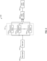
- FIG. 1 is a graphical representation of an embodiment of a communication system.
- a communication system (system) 100 can have a satellite 110 that communicates with a satellite ground station (ground station) 120.
- the ground station 120 can have an antenna 102 coupled to a digitizer 114.
- the digitizer 114 can have one or more analog to digital converters (A2D) for converting analog signals received at the antenna 102 into a digital bit stream for transmission via a network.
- A2D analog to digital converters
- the digitizer 114 can also include corresponding digital to analog converters (D2A) for operations on the uplink to the satellite 110.
- D2A digital to analog converters
- the ground station 120 can transmit an uplink signal 122 to the satellite 110 via the antenna 102 in a transmit chain.
- the ground station 120 can also receive a downlink signal 132 from the satellite 132 via the antenna 102 in a receive chain.
- the digitizer 114 can digitize the received downlink signal 132 for transmission as the digital bit stream 134.
- the digital bit stream 134 can then be transmitted, via a network 124 to a cloud processing system.
- the ground station 120 can process all of the data (e.g., contained in the downlink signal 132) locally, however this can be exceptionally expensive from a time, resource, and efficiency perspective. Therefore, in some embodiments, the downlink signal 132, received from the satellite 110, can be digitized and transmitted as the digital bit stream 134 to a remote signal processing server (SPS) 150.
- the SPS 150 can be positioned in a physical location, such as a data center located in an offsite facility that is accessible via a wide area network (WAN). Such a WAN can be the Internet, for example.
- the SPS 150 can demodulate the downlink signal 132 from the digital bit stream 134 and output the data or information bits from the downlink signal 132. Given the remote location of the SPS 150 and the connection with the network 124, the described signal processing performed by the SPS 150 can be referred to as cloud processing.
- the SPS 150 can also be referred to as a cloud server.
- the SPS 150 can then provide the processed data to the user to be processed within the SPS 150 or sent remotely to a different site.
- the data and information can be mission-dependent.
- the information contained in the data can be the main purpose of the satellite, including weather data, image data, and satellite communication (SATCOM) payload data.
- SATCOM satellite communication
- phase lock loop In order to achieve high processing rates with software, a phase lock loop (PLL) approach can be problematic due to the feedback within the loop.
- the feedback loop forces all of the incoming data (e.g., the downlink signal 132) to be processed on a single (e.g., linear) process that cannot not be easily spilt or otherwise divided.
- the PLL phase lock loop
- there are other obstacles to overcome using the PLL including, for example, how often to calculate the error term.
- FIG. 2 is a functional block diagram of a communication device for use with the system of FIG. 1 .
- a processing device (device) 200 may be implemented as, for example, the SPS 150 of FIG. 1 .
- the device 200 can be implemented as needed to perform one or more of the signal processing methods or steps disclosed herein.
- the device 200 may include a processor 202 which controls operation of the device 200.
- the processor 202 may also be referred to as a central processing unit (CPU).
- the processor 202 can direct and/or perform the functions, for example, attributed to SPS 150.
- the processor 202 may be implemented with any combination of one or more of general-purpose microprocessors, microcontrollers, digital signal processors (DSPs), field programmable gate array (FPGAs), programmable logic devices (PLDs), controllers, state machines, gated logic, discrete hardware components, dedicated hardware finite state machines, or any other suitable entities that can perform calculations or other manipulations of information.
- DSPs digital signal processors
- FPGAs field programmable gate array
- PLDs programmable logic devices
- the processor 202 have contain one or more cores 204 (shown as core 204a through core 204n) on which the computations can be performed.
- the processor 202 can be a complex, integrated circuit on which all the computations for the receiver are taking place.
- the cores 204 can each be one processing element of the processor 202.
- the processor 202 can implement multiple cores 204 to perform the necessary parallel processing for the methods disclosed herein. In some embodiments, the processor 202 may be distributed across multiple CPUs as in cloud computing.
- the device 200 may further include a memory 206 operably coupled to the processor 202, which may include both read-only memory (ROM) and random access memory (RAM), providing instructions and data to the processor 202.
- a portion of the memory 206 may also include non-volatile random access memory (NVRAM).
- the processor 202 typically performs logical and arithmetic operations based on program instructions stored within the memory 206.
- the instructions in the memory 206 may be executable to implement the methods described herein.
- the memory 206 can further include removable media or multiple distributed databases.
- the memory 206 may also include machine-readable media for storing software.
- Software shall be construed broadly to mean any type of instructions, whether referred to as software, firmware, middleware, microcode, hardware description language, or otherwise. Instructions may include code (e.g., in source code format, binary code format, executable code format, or any other suitable format of code). The instructions, when executed by the processor 202 or the one or more cores 204, cause the device 200 (e.g., the SPS 150) to perform the various functions described herein.
- the device 200 may also include a transmitter 210 and a receiver 212 to allow transmission and reception of data between the communication device 200 and a remote location. Such communication can occur between the ground station 120 and the SPS 150 via the network 124, for example. Such communications can be wireless or conducted via wireline communications.
- the transmitter 210 and receiver 212 may be combined into a transceiver 214.
- the transceiver 214 can be communicatively coupled to the network 124.
- the transceiver 214 can include or be a portion of a network interface card (NIC).
- NIC network interface card
- the device 200 may further comprise a user interface 222.
- the user interface 222 may comprise a keypad, a microphone, a speaker, and/or a display.
- the user interface 222 may include any element or component that conveys information to a user of the device 200 and/or receives input from the user.
- the various components of the device 200 described herein may be coupled together by a bus system 226.
- the bus system 226 may include a data bus, for example, as well as a power bus, a control signal bus, and a status signal bus in addition to the data bus.
- the bus system 226 can be communicatively coupled to the network 124.
- the network 124 can provide a communication link between the device 200 (e.g., the processor 202) and the ground station 120, for example.
- the components of the device 200 may be coupled together or accept or provide inputs to each other using some other mechanism such as a local- or wide area network for distributed processing.
- FIG. 3 is a graphical depiction of an embodiment of a method for feedforward signal processing of FIG. 1 .
- a method 300 can occur as the SPS 150 receives digitized versions or digital samples of the downlink signal 132 (the digital bit stream 134). Using the method 300, the SPS 150 can output information contained in the signal 132 as bits (samples in, bits out). Thus, an exemplary benefit of the method 300 is efficient software processing of high-rate data streams.
- the SPS 150 can ingest or otherwise receive the digital bit stream 134 (e.g., via the network 124).
- the data ingest at block 305 can receive the digital bit stream 134 data from a network connection (e.g., Ethernet).
- the data can be split into parallel data streams by a data splitter.
- the processor 202 can perform data splitting functions required in block 310.
- a separate data splitting component e.g., a data splitter
- Splitting the data into multiple parallel streams can allow parallel processing of the downlink signal 132.
- the method 300 can therefore take advantage of feedforward processing to allow the incoming digitized signal data to be broken into smaller pieces and then processed on multiple cores 204.
- the digital bit stream 134 can be split to form overlapping packets in in-phase/quadrature (I/Q) pairs.
- the "overlapping packets" can include data packets in which successive packets are overlapped with adjacent data packets.
- the data packets may all be the same length, but overlapped.
- the overlap in data packets can be at the beginning of the data packet or at the end.
- a data packet can overlap with both the preceding and the following data packets.
- the data packets can also have different lengths (e.g., varying amounts of data). Therefore a first packet sent to the processing block 315a may overlap or otherwise repeat certain data of a second packet sent to the processing block 315b.
- the amount of overlap between packets, or overlap size can be programmable and set as needed.
- the overlap can be set to one percent (1%) of the packet size.
- This overlap size can be increased or decreased depending on need.
- one particular parameter that can impact the overlap size is the uncertainty of the symbol rate in the data stream 134. For most signals, the worst case uncertainty is less than 1%, so a 1% covers most cases.
- the overlap can be 2%, 3%, 4%, 5%, 6%, 7%, 8%, 9%, or as high as 10%, or anywhere in between, as needed. It is also possible to have less than 1% overlap as well. The overlap could be 0.1% or lower if the data rate uncertainty is less than 0.1%.
- the processor 202 can implement single instruction, multiple data (SIMD) processing on the digital bit stream 134.
- SIMD can include Advanced Vector Extensions using 512 bits (AVX-512) allowing 16 floating point operations on a single CPU core on a single CPU instruction.
- AVX-512 can process enormous amounts of data with the CPU (e.g., the CPU 202).
- the processor 202 (and the device 200) can receive a 500 MHZ bandwidth data stream.
- 500 MHz of bandwidth is significant in some respects because that is a generally accepted practical limit of a 10 Gigabit Ethernet link.
- Sampling the data at 500 MHz, with 8 bits samples for an I/Q pair and including parity bits can saturate a 10 Gbit Ethernet link.
- the 500 MHz example is not limiting on the disclosure. Data pipes larger than a 10 Gbit Ethernet link are possible.
- the processing can be split into n-number of parallel blocks (e.g., block 315) to accommodate any amount of data.
- Block 315 is shown in dashed lines and depicts a processing step of the method 300.
- Block 315 is shown in multiple, parallel steps, or block 315a, 315b through 315n.
- the term "parallel" is used herein to describe that processing occurs in the processing blocks 315a-315n at the same time.
- the packets being processed may be of different lengths from one processing block 315 to another, so the processing of packets may have the same rate or speed from one processing block 315 to the next. As noted below, some of the processing bocks 315 may proceed faster or slower than others. Accordingly, the term parallel should not be limited to simultaneous or concurrent processing within the processing blocks 315.
- the processing blocks 315 as used herein, can refer to a collection of processing functions performed by the processor 202, for example.
- the digital bit stream 134 can be sent into multiple parallel processing blocks 315a, 315b ... 315n to spread the processing load across several cores 204.
- the processing of each of the processing blocks 315a-315n can be associated with a core 204a-204n.
- the number of processing blocks 315 needed varies based on the amount of data being processed. In some embodiments, the number of processing blocks 315 can be limited by the number of logical cores within the processor 202. In some other embodiments, memory bandwidth constraints can cause a bottle neck in the signal processing.
- Memory bandwidth can refer to the rate at which data can be read from or stored into a semiconductor memory (e.g., the memory 206) by a processor (e.g., the processor 202).
- the number of processing blocks 315 can vary. In general, the fewer processing blocks 315 present, the better to limit the number of cores needed for the entire process. This can further enable the system to fit into smaller virtual private cloud (VPC) machines which are cheaper to operate.
- VPC virtual private cloud
- a VPC can include the SPS 150 having several CPUs, for example.
- 8 processing blocks 315 can be used for a 10Gbit Ethernet link. Such an embodiment may not include forward error correction processing blocks.
- the only practical limitation on the number of processing blocks 315 needed is the bitrate and bandwidth of the communication link (e.g., size of the pipe). Accordingly, any number (n) of processing blocks 315 is possible.
- a practical limitation on the number (n) processing blocks 315 may be present based on the number of threads that can be run on a CPU or the number of cores 204 in the processor 202. However, if the limits are reached within a single CPU, multiple CPUs (e.g., the processor 202) together within the SPS 150 (e.g., a VPC) and have, an unlimited number of CPUs or cores 204 to perform the processing. In addition, the processor 202 can create new processing block 315 as needed. The processing cores 204 can be spread across multiple distributed processors (e.g., the processor 202) as needed for throughput and efficiency.
- the processing blocks 315 are arranged in such a way that it does not matter which processing block 315a, 315b ... 315n are performed the slowest (or fastest).
- the method 300 can share the processing load across the processing blocks 315 and therefore alleviate any processing delays caused by bottle necking issues at individual processing blocks 315.
- individual subprocesses of the processing blocks 315 may not be performed or occur at equal rates (e.g., some are faster than others). Accordingly, larger process of the method 400 ( FIG. 4 ), for example, can account for variations in performance or processing times.
- the processing blocks 315 can then be created as many times as needed to handle the incoming data.
- each processing block 315 can represent a collection of signal processing algorithms performed by the processor 202.
- an algorithm can refer to the smallest collection of functions or method steps that perform a desired function. Multiple exemplary algorithms are described herein.
- An exemplary benefit of the method 300 is the ability to create more processing blocks 315 when needed.
- the processing blocks 315 can be implemented in software, and so can be created or eliminated as needed to suit a given data rate or processing load.
- Each processing block 315 can be rearranged to fit the needs of different received waveforms (e.g., the downlink signal 132) and the associated digital bit streams 134. Two possible arrangements of processing blocks are described below in connection with FIG. 4 and FIG. 5 .
- the processed signal data from the multiple processing blocks 315 can be recombined to form the original data encoded and modulated on the downlink signal 134.
- the processor 202 can perform the functions of a data recombiner.
- the device 200 can have an additional component to perform such functions.
- Each data packet or processed block of data can have a time stamp.
- the data recombiner e.g., the processor 202 can order the data blocks based on the time stamps and compare the phase between the ordered blocks.
- the recombiner can further adjust the phase of adjacent blocks reorder the data stream.
- the phase of a subsequent data block can be adjusted to match the phase of a previous data block.
- the device 200 can output the data to an appropriate receiver.
- a receiver can be one or more mission operations centers.
- This data can be mission dependent (e.g., the purpose of the satellite), and can include, among other things, weather data, image data, and SATCOM payload data.
- FIG. 4 is a flowchart of an example of a method for signal processing of FIG. 3 .
- a method 400 is shown and can be implemented as the processes that occur in each of blocks 315a-315n of FIG. 3 .
- the method 400 can be used for standard waveform processing as opposed to offset waveforms described below.
- standard waveform processing can be used for waveforms that map bits into symbols and then modulate the symbols onto a carrier wave. Examples of standard waveforms include binary phase shift keying (BPSK), quadrature phase shift keying (QPSK), 8PSK, 16APSK, 32APSK and 64 APSK as well as quadrature amplitude modulation (QAM) waveforms.
- BPSK binary phase shift keying
- QPSK quadrature phase shift keying
- 8PSK 8PSK
- 16APSK 32APSK
- 64 APSK quadrature amplitude modulation
- the processor 202 can perform a timing recovery error calculation on the received data packets (e.g., samples of the digitized bitstream 134 or the digitized downlink signal 132).
- the timing recovery error calculation can provide the needed phase information to properly align a matched filter to the incoming data stream (e.g., the digitized bit stream 134).
- the match filter is used to match the transmitted waveform in the time domain and is aligned by the timing error to capture all the energy in the received signal to optimize performance.
- the results of the timing recovery error calculation can include three parameters: 1) starting phase in degrees; 2) frequency adjustment in Hertz (Hz); and 3) Doppler rate adjustment in Hz/sec.
- the foregoing units are exemplary and are not limiting on the disclosure. Other equivalent units are also possible.
- the processor 202 e.g., one of the cores 204 can perform a timing recovery on the packets to align an internally generated match filter to the received samples that were generated with the modulator's respective match filter.
- the alignment is based on the calculation in block 405.
- the output of block 410 is the synchronized (e.g., time-corrected) symbols within the data packets received at block 405.
- the processor 202 e.g., one of the cores 204 can perform a carrier recovery error calculation on the packets to determine phase and frequency information.
- a carrier recovery error calculation can be performed on the packets to determine phase and frequency information.
- the processor 202 can perform a carrier recovery on the packets based on the calculation in block 415.
- Carrier recovery compensates for unknown frequency, Doppler rate, and phase offsets in the downlink signal 132 from the spacecraft (e.g., the satellite 110).
- the two most common sources of uncertainty are the Doppler effects from the spacecraft motion and from imperfect oscillators within the spacecraft.
- the processor 202 can apply the phase, frequency, and Doppler rate corrections from block 415 to form a synchronous symbols corresponding to the modulated data in the downlink signal 132 at the output of block 420.
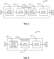
- FIG. 5 is a flowchart of an embodiment of a method for signal processing of FIG. 3 (the processes that occur in each of blocks 315a-315n).
- a method 500 can be similar to the method 400 ( FIG. 4 ), combining and rearranging some of the steps.
- the method 500 can be used for offset waveform processing.
- offset waveform processing can be used for waveforms having an offset or stagger between the In-phase (I) and Quadrature (Q) channels, such as waveforms like Offset quadrature phase-shift keying (OQPSK), minimum-shift keying (MSK), Gaussian minimum-shift keying (GMSK), and shaped-offset quadrature phase shift (SOQPSK).
- OQPSK Offset quadrature phase-shift keying
- MSK minimum-shift keying
- GMSK Gaussian minimum-shift keying
- SOQPSK shaped-offset quadrature phase shift
- the processor 202 can perform a timing and carrier recovery error calculation on the packets.
- the timing recovery error calculation and the carrier recovery error calculation are similar to those performed in block 420 ( FIG. 4 ).
- the carrier recovery is performed before timing recovery of the symbols.
- the input to the method 400 is the data samples and the output is corrected, synchronous symbols.
- the processor 202 can perform a carrier recovery operation based on the calculation from block 505.
- the substeps of block 505 are described below in connection with FIG. 8 .
- the processor 202 can perform a timing recovery operation based on the calculation from block 505.
- FIG. 6 is a flowchart of an example method for timing recovery error calculation for block 405 in FIG. 4 .
- the processor 202 can apply a Gardner Timing Error Detector to the incoming data to create the timing information, as is known in the art.
- the incoming sample stream can be delayed by one sample. Then the nondelayed data can be multiplied by the conjugate (conjugate multiplication) of the delayed data. Both have advantages and drawbacks so it is an engineering tradeoff on which may be implemented.
- Timing spike appears as a single frequency tone in the frequency domain.
- the timing spike contains the timing estimation information, including starting phase in cycles, degrees, or radians, timing frequency offset in Hz and timing Doppler estimation in Hz/sec.
- the timing spike can be mixed to DC by the estimated symbol rate and then filtered and decimated to improve signal-to-noise ratio to improve the accuracy of the phase, frequency and Doppler Rate estimate.
- the carrier frequency and symbol rate estimate is initially derived from an acquisition function. The carrier frequency and symbol rate estimation is calculated similarly to the feed forward error recovery algorithms.
- the decimation is much less to enable a wider frequency range to be detected and 2) the phase unwrap and curve fit calculation is replaced with an FFT followed by a peak search calculation.
- the estimate is later updated (e.g., within the block 630).
- Both methods have the benefit of being fairly insensitive to carrier uncertainty and therefore can be run before carrier recovery.
- Another benefit to running the timing recovery step first is this drops the sample rate down from about two times (2x) the symbol rate to exactly 1x the symbol rate and therefore the carrier recovery algorithm runs at the lowest rate possible.
- Another benefit is the carrier recovery loop can then operate with an improved signal-to-noise ratio since the sample rate is now half the original sample rate.
- the processor 202 can mix the timing spike generated at block 605 with a timing estimate or an estimate of the symbol rate. As the method 300 is initiated, certain information about the downlink signal 132 may not be known. Accordingly, at block 610 the processor 202 may use an initial estimate of the symbol rate to mix with the timing spike from block 605. This estimate is later updated, as described below. This process can mix the time spike to DC so it can be easily filtered by a decimation filter. The block 605 and the block 610 can provide a timing error of the data packets/data samples.
- the processor 202 can decimate the mixed signal to reduce the sampling rate. Decimation can improve the signal-to-noise ratio since the power in the timing spike (the signal) is passed entirely through the filter but the noise power is reduced proportional to the decimation rate.
- the processor 202 can perform a phase unwrap calculation on the decimated samples. This can include a phase calculation of the decimated signal that is performed before the phase unwrap.
- the phase unwrap calculation can provide continuous phase information about the data samples.
- the phase unwrap calculation stitches the phase together when the phase wraps either from ⁇ (pi) to - ⁇ or - ⁇ to ⁇ radians. This unwrapping on the angle allows for a curve fitting function to run on a phase signal without any discontinuities. This can allow the processor 202 to reassemble the demodulated signal based on timing and phase of the processed packets.
- the processor 202 can perform a curve fit calculation to determine phase, frequency, and Doppler rate offset information that can be applied to update the timing estimate at block 630.
- the curve fit can result in a quadratic representation of the phase, frequency, and Doppler rate information of the data samples, and ultimately the downlink signal 132.
- Ax ⁇ 2+Bx+C A represents Doppler Rate, B, frequency, and C, phase.
- the output of the method 600 is the originally received samples and associated metadata (e.g., the phase, frequency, and Doppler rate information).
- phase unwrap and curve fit calculation with a Kalman filter to obtain the phase, frequency and Doppler Rate information.
- FIG. 7 is a flowchart of an example of a method for determining carrier recovery error for block 415 of FIG. 4 .
- a method 700 can be used to calculate the needed phase, frequency, and Doppler rate information to create a mixing signal to properly demodulate the incoming symbol synchronized signal.
- the incoming signal can be raised to certain power based on modulation type (e.g., BPSK raises to the power of 2; QPSK raises to the power of 4; 8PSK raises to the power of 8). Raising the signal to a power may be multiplying the signal by itself n-number of times, where n is an integer. This may also be referred to herein as exponentiating the signal.
- the result of such calculation is a carrier spike in the frequency domain (e.g., a continuous wave signal) that can be mixed to DC with a carrier estimate at block 710.
- the estimate can be generated using the acquisition function described above in connection with FIG. 6 .
- the processor 202 can decimate the mixed signal to reduce the sampling rate, similar to block 615 ( FIG. 6 ) above. Decimation can improve the signal-to-noise ratio since the power in the timing spike (the signal) is passed entirely through the filter but the noise power is reduced proportional to the decimation rate.
- the processor 202 can perform a phase unwrap calculation on the decimated samples similar to block 620 ( FIG. 6 ) above.
- the processor 202 can perform a curve fit calculation to determine phase, frequency, and Doppler rate offset information that can be applied to update the carrier recovery algorithm (block 415 of FIG. 4 ).
- the curve fit can be used to update (and improve) the carrier frequency estimate of block 710. It is possible to replace the phase unwrap and curve fit calculation with a Kalman filter to obtain the phase, frequency and Doppler Rate information.
- FIG. 8 is a flowchart of a method for the timing and carrier recovery error calculation for block 505 of FIG. 5 .
- a method 800 can be performed at block 505 of FIG. 5 .
- Some such waveforms can include OQPSK, MSK, and GMSK, for example.
- the digitized bit stream 134 can be squared (power of 2) at block 805. This can result in two spikes being created in the frequency domain. Each spike can then be mixed near 0 Hz by the mix signal that is created from a composite estimate of the carrier frequency and symbol rate. The estimate can be generated using the acquisition function described above in connection with FIG. 6 .
- both mixed signals are then decimated to reduce the sampling rate.
- the processor 202 can perform a phase unwrap calculation on both mixed signals similar to 620 and 720.
- the processor 202 can perform a curve-fit calculation similar to 625 and 725 except in block 825 there are two curve fit calculations that occur.
- the sum of the two curve fit calculations is the carrier phase and frequency estimate and the difference is the timing phase and frequency estimate.
- the curve fit can result in a quadratic representation of the phase, frequency, and Doppler rate information of the data samples, and ultimately the downlink signal 132.
- Ax ⁇ 2+Bx+C A represents Doppler Rate, B- frequency, and C- phase.
- the output of the method 800 is the originally received samples and associated metadata (e.g., the phase, frequency, and Doppler rate information).
- the system can output data for both the carrier and timing estimates so there is an Ax ⁇ 2+Bx+C for the carrier and Ax ⁇ 2+Bx+C for timing at block 825.
- this information is updated (similar to block 630 and block 730) and passed onto the carrier recovery and timing recovery algorithms in the order as shown in FIG. 8 .
- DSP digital signal processor
- ASIC application specific integrated circuit
- FPGA field programmable gate array
- a general-purpose processor may be a microprocessor, but, in the alternative, the processor may be any conventional processor, controller, microcontroller, or state machine.
- a processor may also be implemented as a combination of receiver devices, e.g., a combination of a DSP and a microprocessor, a plurality of microprocessors, one or more microprocessors in conjunction with a DSP core, or any other such configuration. Alternatively, some operations or methods may be performed by circuitry that is specific to a given function.
- the functions described may be implemented in hardware, software, firmware, or any combination thereof. If implemented in software, the functions may be stored as one or more instructions or code on a non-transitory computer-readable storage medium or non-transitory processor-readable storage medium.
- the operations of a method or algorithm disclosed herein may be embodied in processor-executable instructions that may reside on a non-transitory computer-readable or processor-readable storage medium.
- Non-transitory computer-readable or processor-readable storage media may be any storage media that may be accessed by a computer or a processor.
- non-transitory computer-readable or processor-readable storage media may include random access memory (RAM), read-only memory (ROM), electrically erasable programmable read-only memory (EEPROM), FLASH memory, CD-ROM or other optical disk storage, magnetic disk storage or other magnetic storage devices, or any other medium that may be used to store desired program code in the form of instructions or data structures and that may be accessed by a computer.
- Disk and disc includes compact disc (CD), laser disc, optical disc, digital versatile disc (DVD), floppy disk, and Blu-ray disc where disks usually reproduce data magnetically, while discs reproduce data optically with lasers.
Landscapes
- Engineering & Computer Science (AREA)
- Computer Networks & Wireless Communication (AREA)
- Signal Processing (AREA)
- General Physics & Mathematics (AREA)
- Physics & Mathematics (AREA)
- Astronomy & Astrophysics (AREA)
- Aviation & Aerospace Engineering (AREA)
- Theoretical Computer Science (AREA)
- General Engineering & Computer Science (AREA)
- Human Computer Interaction (AREA)
- Multimedia (AREA)
- Computer Hardware Design (AREA)
- Digital Transmission Methods That Use Modulated Carrier Waves (AREA)
- Sorting Of Articles (AREA)
- Signal Processing For Digital Recording And Reproducing (AREA)
- Communication Control (AREA)
- Data Exchanges In Wide-Area Networks (AREA)
- Mobile Radio Communication Systems (AREA)
- Radio Transmission System (AREA)
Description
- This disclosure relates to signal processing. More specifically, this disclosure relates to feed forward carrier and timing recovery for phase shift keying (PSK) waveforms utilizing single instruction-multiple data (SIMD) architectures.
- In some examples, a satellite communication signal can require large ground stations and other facilities to transmit and/or receive and process data locally. This can include extensive antenna arrays, associated radio frequency terminals (RFTs), and significant electronics (modems, signal processors, etc.) to receive, process, and use the data received from an associated satellite.
-
US 2006/291599A1 discloses a communication system which employs site diversity combing to increase link availability, and includes at least two receivers at receive sites which are within a single downlink beam, separated by sufficient distance to provide decorrelation of weather phenomena, such as rain fade outages. A signal transmits digital symbols to all receivers and may use bandwidth efficient modulation with forward error correction coding. Sampled symbol values for each codeword are produced at each receiver, which are connected by one or more ground links so that all of the data can be collected at one site. At least two different soft-decision computation modules translate the sampled symbol values from the different receivers into different sets of soft-decision values, which may be log-likelihood-ratio (LLR) values reflecting the probability value for each bit of the codeword, that are digitally synchronised and combined for use by a decoder. - S. A. Callaghan et al. ("An investigation of site diversity and comparison with ITU-R recommendations: Site diversity and ITU-R recommendations", RADIO SCIENCE, volume 43, no.4, 1st August 2008) investigated unbalanced site diversity in their paper, and the commercial factors of its implementation. Unbalanced site diversity differs to balanced site diversity in that, rather than both paths in a diversity pair (which are two spatially separated ground stations connected by a communications link) having the identical sensitivity in terms of fade margin, the second path has a smaller margin (or antenna).
- This disclosure addresses systems and methods for satellite communications using downlink site diversity and uplink transmit power management. A plurality of ground stations can include a piggyback signal in transmissions to ensure coherent reception of multiple versions of a signal using site diversity. The object of the invention is achieved by the subject-matter of the independent claims. The dependent claims describe advantageous optional embodiments. The scope of protection of the invention is solely limited by the appended claims.
- An aspect of the disclosure provides a method for processing a digital bit stream representative of a communication signal. The method includes dividing, at one or more processors, the digital bit stream into a plurality of data packets, each of the data packets of the plurality of data packets including an overlap of data from an adjacent packet. The method includes, in a first one or more processing blocks in the processor, performing a timing recovery error calculation and a timing recovery operation on a first portion of the plurality of data packets, and performing a carrier recovery error calculation and a carrier recovery operation on the first portion of the plurality of data packets. The method includes, in a second one or more processing blocks in the processor, in parallel with the first portion of the plurality of packets, performing a timing recovery error calculation and timing recovery operation on a second portion of the plurality of data packets, and performing a carrier recovery error calculation and carrier recovery operation on the second portion of the plurality of data packets. The method includes combining the first portion and the second portion based on timing and phase stitching.
- Another aspect of the disclosure provides a system for processing a digital bit stream representative of a communication signal. The system has a digitizer operable to convert a received analog signal into the digital bitstream. The system has one or more processors communicatively coupled to a plurality of processing blocks and operable to perform the method of the previous aspect.
- Other features and benefits will be apparent to one of skill in the art with a review of the following description.
- The details of embodiments of the present disclosure, both as to their structure and operation, can be gleaned in part by study of the accompanying drawings, in which like reference numerals refer to like parts, and in which:
-
FIG. 1 is a graphical representation of an embodiment of a satellite communication system; -
FIG. 2 is a functional block diagram of a communication device for use with the system ofFIG. 1 ; -
FIG. 3 is a graphical depiction of an embodiment of a method for feedforward signal processing ofFIG. 1 ; -
FIG. 4 is a flowchart of a method for signal processing ofFIG. 3 ; -
FIG. 5 is a flowchart of a method for signal processing ofFIG. 3 ; and -
FIG. 6 is a flowchart of a method for timing recovery error calculation; -
FIG. 7 is a flowchart of a method for determining carrier recovery error; and -
FIG. 8 is a flowchart of a method for a timing and carrier recovery error calculation. - Reference throughout this specification to "one embodiment" or "an embodiment" means that a particular feature, structure, or characteristic described in connection with the embodiment is included in at least one embodiment. Thus, appearances of the phrases "in one embodiment" or "in an embodiment" in various places throughout this specification are not necessarily all referring to the same embodiment. Furthermore, the particular features, structures, or characteristics may be combined in any suitable manner in one or more embodiments.
- A satellite communication system is used as a primary example throughout the description, however, the application of the disclosed methods is not so limited. For example, any communication system requiring the use of a modem can implement the systems, methods, and computer readable media described herein.
-
FIG. 1 is a graphical representation of an embodiment of a communication system. A communication system (system) 100 can have asatellite 110 that communicates with a satellite ground station (ground station) 120. Theground station 120 can have anantenna 102 coupled to adigitizer 114. Thedigitizer 114 can have one or more analog to digital converters (A2D) for converting analog signals received at theantenna 102 into a digital bit stream for transmission via a network. Thedigitizer 114 can also include corresponding digital to analog converters (D2A) for operations on the uplink to thesatellite 110. - The
ground station 120 can transmit anuplink signal 122 to thesatellite 110 via theantenna 102 in a transmit chain. Theground station 120 can also receive adownlink signal 132 from thesatellite 132 via theantenna 102 in a receive chain. Thedigitizer 114 can digitize the receiveddownlink signal 132 for transmission as thedigital bit stream 134. Thedigital bit stream 134 can then be transmitted, via anetwork 124 to a cloud processing system. - In some examples, the
ground station 120 can process all of the data (e.g., contained in the downlink signal 132) locally, however this can be exceptionally expensive from a time, resource, and efficiency perspective. Therefore, in some embodiments, thedownlink signal 132, received from thesatellite 110, can be digitized and transmitted as thedigital bit stream 134 to a remote signal processing server (SPS) 150. The SPS 150 can be positioned in a physical location, such as a data center located in an offsite facility that is accessible via a wide area network (WAN). Such a WAN can be the Internet, for example. The SPS 150 can demodulate thedownlink signal 132 from thedigital bit stream 134 and output the data or information bits from thedownlink signal 132. Given the remote location of the SPS 150 and the connection with thenetwork 124, the described signal processing performed by the SPS 150 can be referred to as cloud processing. The SPS 150 can also be referred to as a cloud server. - The SPS 150 can then provide the processed data to the user to be processed within the SPS 150 or sent remotely to a different site. The data and information can be mission-dependent. In addition, the information contained in the data can be the main purpose of the satellite, including weather data, image data, and satellite communication (SATCOM) payload data.
- In order to achieve high processing rates with software, a phase lock loop (PLL) approach can be problematic due to the feedback within the loop. The feedback loop forces all of the incoming data (e.g., the downlink signal 132) to be processed on a single (e.g., linear) process that cannot not be easily spilt or otherwise divided. In addition to the feedback, there are other obstacles to overcome using the PLL including, for example, how often to calculate the error term.
-
FIG. 2 is a functional block diagram of a communication device for use with the system ofFIG. 1 . A processing device (device) 200 may be implemented as, for example, the SPS 150 ofFIG. 1 . Thedevice 200 can be implemented as needed to perform one or more of the signal processing methods or steps disclosed herein. - The
device 200 may include aprocessor 202 which controls operation of thedevice 200. Theprocessor 202 may also be referred to as a central processing unit (CPU). Theprocessor 202 can direct and/or perform the functions, for example, attributed to SPS 150. Theprocessor 202 may be implemented with any combination of one or more of general-purpose microprocessors, microcontrollers, digital signal processors (DSPs), field programmable gate array (FPGAs), programmable logic devices (PLDs), controllers, state machines, gated logic, discrete hardware components, dedicated hardware finite state machines, or any other suitable entities that can perform calculations or other manipulations of information. - The
processor 202 have contain one or more cores 204 (shown ascore 204a throughcore 204n) on which the computations can be performed. Theprocessor 202 can be a complex, integrated circuit on which all the computations for the receiver are taking place. As used herein, the cores 204 can each be one processing element of theprocessor 202. Theprocessor 202 can implement multiple cores 204 to perform the necessary parallel processing for the methods disclosed herein. In some embodiments, theprocessor 202 may be distributed across multiple CPUs as in cloud computing. - The
device 200 may further include amemory 206 operably coupled to theprocessor 202, which may include both read-only memory (ROM) and random access memory (RAM), providing instructions and data to theprocessor 202. A portion of thememory 206 may also include non-volatile random access memory (NVRAM). Theprocessor 202 typically performs logical and arithmetic operations based on program instructions stored within thememory 206. The instructions in thememory 206 may be executable to implement the methods described herein. Thememory 206 can further include removable media or multiple distributed databases. - The
memory 206 may also include machine-readable media for storing software. Software shall be construed broadly to mean any type of instructions, whether referred to as software, firmware, middleware, microcode, hardware description language, or otherwise. Instructions may include code (e.g., in source code format, binary code format, executable code format, or any other suitable format of code). The instructions, when executed by theprocessor 202 or the one or more cores 204, cause the device 200 (e.g., the SPS 150) to perform the various functions described herein. - The
device 200 may also include atransmitter 210 and areceiver 212 to allow transmission and reception of data between thecommunication device 200 and a remote location. Such communication can occur between theground station 120 and the SPS 150 via thenetwork 124, for example. Such communications can be wireless or conducted via wireline communications. Thetransmitter 210 andreceiver 212 may be combined into atransceiver 214. Thetransceiver 214 can be communicatively coupled to thenetwork 124. In some examples thetransceiver 214 can include or be a portion of a network interface card (NIC). - The
device 200 may further comprise a user interface 222. The user interface 222 may comprise a keypad, a microphone, a speaker, and/or a display. The user interface 222 may include any element or component that conveys information to a user of thedevice 200 and/or receives input from the user. - The various components of the
device 200 described herein may be coupled together by abus system 226. Thebus system 226 may include a data bus, for example, as well as a power bus, a control signal bus, and a status signal bus in addition to the data bus. In some embodiments, thebus system 226 can be communicatively coupled to thenetwork 124. Thenetwork 124 can provide a communication link between the device 200 (e.g., the processor 202) and theground station 120, for example. Those of skill in the art will appreciate the components of thedevice 200 may be coupled together or accept or provide inputs to each other using some other mechanism such as a local- or wide area network for distributed processing. -
FIG. 3 is a graphical depiction of an embodiment of a method for feedforward signal processing ofFIG. 1 . Amethod 300 can occur as the SPS 150 receives digitized versions or digital samples of the downlink signal 132 (the digital bit stream 134). Using themethod 300, the SPS 150 can output information contained in thesignal 132 as bits (samples in, bits out). Thus, an exemplary benefit of themethod 300 is efficient software processing of high-rate data streams. - At
block 305, the SPS 150 can ingest or otherwise receive the digital bit stream 134 (e.g., via the network 124). The data ingest atblock 305 can receive thedigital bit stream 134 data from a network connection (e.g., Ethernet). - At
block 310, the data can be split into parallel data streams by a data splitter. In some embodiments, theprocessor 202 can perform data splitting functions required inblock 310. In some other embodiments, a separate data splitting component (e.g., a data splitter) can be included in the device 200 (FIG. 2 ). Splitting the data into multiple parallel streams can allow parallel processing of thedownlink signal 132. Themethod 300 can therefore take advantage of feedforward processing to allow the incoming digitized signal data to be broken into smaller pieces and then processed on multiple cores 204. Thedigital bit stream 134 can be split to form overlapping packets in in-phase/quadrature (I/Q) pairs. In some embodiments, the "overlapping packets" can include data packets in which successive packets are overlapped with adjacent data packets. In some embodiments the data packets may all be the same length, but overlapped. The overlap in data packets can be at the beginning of the data packet or at the end. In addition, a data packet can overlap with both the preceding and the following data packets. The data packets can also have different lengths (e.g., varying amounts of data). Therefore a first packet sent to theprocessing block 315a may overlap or otherwise repeat certain data of a second packet sent to theprocessing block 315b. - The amount of overlap between packets, or overlap size can be programmable and set as needed. In some examples, the overlap can be set to one percent (1%) of the packet size. This overlap size can be increased or decreased depending on need. For example, one particular parameter that can impact the overlap size is the uncertainty of the symbol rate in the
data stream 134. For most signals, the worst case uncertainty is less than 1%, so a 1% covers most cases. In some other embodiments, the overlap can be 2%, 3%, 4%, 5%, 6%, 7%, 8%, 9%, or as high as 10%, or anywhere in between, as needed. It is also possible to have less than 1% overlap as well. The overlap could be 0.1% or lower if the data rate uncertainty is less than 0.1%. - The
processor 202 can implement single instruction, multiple data (SIMD) processing on thedigital bit stream 134. In some examples, SIMD can include Advanced Vector Extensions using 512 bits (AVX-512) allowing 16 floating point operations on a single CPU core on a single CPU instruction. AVX-512, for example, can process enormous amounts of data with the CPU (e.g., the CPU 202). For example, the processor 202 (and the device 200) can receive a 500 MHZ bandwidth data stream. 500 MHz of bandwidth is significant in some respects because that is a generally accepted practical limit of a 10 Gigabit Ethernet link. Sampling the data at 500 MHz, with 8 bits samples for an I/Q pair and including parity bits, can saturate a 10 Gbit Ethernet link. The 500 MHz example is not limiting on the disclosure. Data pipes larger than a 10 Gbit Ethernet link are possible. In addition, the processing can be split into n-number of parallel blocks (e.g., block 315) to accommodate any amount of data. -
Block 315 is shown in dashed lines and depicts a processing step of themethod 300.Block 315 is shown in multiple, parallel steps, orblock processing blocks 315a-315n at the same time. The packets being processed may be of different lengths from oneprocessing block 315 to another, so the processing of packets may have the same rate or speed from oneprocessing block 315 to the next. As noted below, some of theprocessing bocks 315 may proceed faster or slower than others. Accordingly, the term parallel should not be limited to simultaneous or concurrent processing within the processing blocks 315. - The processing blocks 315 as used herein, can refer to a collection of processing functions performed by the
processor 202, for example. Thedigital bit stream 134 can be sent into multipleparallel processing blocks processing blocks 315a-315n can be associated with acore 204a-204n. The number of processing blocks 315 needed varies based on the amount of data being processed. In some embodiments, the number of processing blocks 315 can be limited by the number of logical cores within theprocessor 202. In some other embodiments, memory bandwidth constraints can cause a bottle neck in the signal processing. Memory bandwidth can refer to the rate at which data can be read from or stored into a semiconductor memory (e.g., the memory 206) by a processor (e.g., the processor 202). - In some embodiments, the number of processing blocks 315 can vary. In general, the fewer processing blocks 315 present, the better to limit the number of cores needed for the entire process. This can further enable the system to fit into smaller virtual private cloud (VPC) machines which are cheaper to operate. A VPC can include the SPS 150 having several CPUs, for example. In some embodiments, 8 processing blocks 315 can be used for a 10Gbit Ethernet link. Such an embodiment may not include forward error correction processing blocks. In some other embodiments, the only practical limitation on the number of processing blocks 315 needed is the bitrate and bandwidth of the communication link (e.g., size of the pipe). Accordingly, any number (n) of processing blocks 315 is possible. In some embodiments, however a practical limitation on the number (n) processing blocks 315 may be present based on the number of threads that can be run on a CPU or the number of cores 204 in the
processor 202. However, if the limits are reached within a single CPU, multiple CPUs (e.g., the processor 202) together within the SPS 150 (e.g., a VPC) and have, an unlimited number of CPUs or cores 204 to perform the processing. In addition, theprocessor 202 can createnew processing block 315 as needed. The processing cores 204 can be spread across multiple distributed processors (e.g., the processor 202) as needed for throughput and efficiency. - The processing blocks 315 are arranged in such a way that it does not matter which
processing block method 300 can share the processing load across the processing blocks 315 and therefore alleviate any processing delays caused by bottle necking issues at individual processing blocks 315. For example, individual subprocesses of the processing blocks 315 (see description ofFIG. 4 , below) may not be performed or occur at equal rates (e.g., some are faster than others). Accordingly, larger process of the method 400 (FIG. 4 ), for example, can account for variations in performance or processing times. The processing blocks 315 can then be created as many times as needed to handle the incoming data. - In some embodiments, each
processing block 315 can represent a collection of signal processing algorithms performed by theprocessor 202. As used herein, an algorithm can refer to the smallest collection of functions or method steps that perform a desired function. Multiple exemplary algorithms are described herein. - An exemplary benefit of the
method 300 is the ability to create more processing blocks 315 when needed. In general, the processing blocks 315 can be implemented in software, and so can be created or eliminated as needed to suit a given data rate or processing load. Eachprocessing block 315 can be rearranged to fit the needs of different received waveforms (e.g., the downlink signal 132) and the associated digital bit streams 134. Two possible arrangements of processing blocks are described below in connection withFIG. 4 and FIG. 5 . - At
block 320 the processed signal data from the multiple processing blocks 315 can be recombined to form the original data encoded and modulated on thedownlink signal 134. In some embodiments, theprocessor 202 can perform the functions of a data recombiner. In other embodiments, thedevice 200 can have an additional component to perform such functions. Each data packet or processed block of data can have a time stamp. The data recombiner (e.g., the processor 202) can order the data blocks based on the time stamps and compare the phase between the ordered blocks. The recombiner can further adjust the phase of adjacent blocks reorder the data stream. In some embodiments, the phase of a subsequent data block can be adjusted to match the phase of a previous data block. - At
block 325, thedevice 200 can output the data to an appropriate receiver. In some examples such a receiver can be one or more mission operations centers. This data can be mission dependent (e.g., the purpose of the satellite), and can include, among other things, weather data, image data, and SATCOM payload data. -
FIG. 4 is a flowchart of an example of a method for signal processing ofFIG. 3 . Amethod 400 is shown and can be implemented as the processes that occur in each ofblocks 315a-315n ofFIG. 3 . Themethod 400 can be used for standard waveform processing as opposed to offset waveforms described below. For example, standard waveform processing can be used for waveforms that map bits into symbols and then modulate the symbols onto a carrier wave. Examples of standard waveforms include binary phase shift keying (BPSK), quadrature phase shift keying (QPSK), 8PSK, 16APSK, 32APSK and 64 APSK as well as quadrature amplitude modulation (QAM) waveforms. - At
block 405 the processor 202 (e.g., one or more of the cores 204) can perform a timing recovery error calculation on the received data packets (e.g., samples of the digitizedbitstream 134 or the digitized downlink signal 132). The timing recovery error calculation can provide the needed phase information to properly align a matched filter to the incoming data stream (e.g., the digitized bit stream 134). The match filter is used to match the transmitted waveform in the time domain and is aligned by the timing error to capture all the energy in the received signal to optimize performance. An example of the process ofblock 405 is described in connection withFIG. 6 . The results of the timing recovery error calculation can include three parameters: 1) starting phase in degrees; 2) frequency adjustment in Hertz (Hz); and 3) Doppler rate adjustment in Hz/sec. The foregoing units are exemplary and are not limiting on the disclosure. Other equivalent units are also possible. - At
block 410 the processor 202 (e.g., one of the cores 204) can perform a timing recovery on the packets to align an internally generated match filter to the received samples that were generated with the modulator's respective match filter. The alignment is based on the calculation inblock 405. The output ofblock 410 is the synchronized (e.g., time-corrected) symbols within the data packets received atblock 405. - At
block 415 the processor 202 (e.g., one of the cores 204) can perform a carrier recovery error calculation on the packets to determine phase and frequency information. A more detailed explanation of an example of the functions performed inblock 415 is described below in connection withFIG. 7 . - At
block 420 the processor 202 (e.g., one of the cores 204) can perform a carrier recovery on the packets based on the calculation inblock 415. Carrier recovery compensates for unknown frequency, Doppler rate, and phase offsets in thedownlink signal 132 from the spacecraft (e.g., the satellite 110). The two most common sources of uncertainty are the Doppler effects from the spacecraft motion and from imperfect oscillators within the spacecraft. Theprocessor 202 can apply the phase, frequency, and Doppler rate corrections fromblock 415 to form a synchronous symbols corresponding to the modulated data in thedownlink signal 132 at the output ofblock 420. -
FIG. 5 is a flowchart of an embodiment of a method for signal processing ofFIG. 3 (the processes that occur in each ofblocks 315a-315n). Amethod 500 can be similar to the method 400 (FIG. 4 ), combining and rearranging some of the steps. Themethod 500 can be used for offset waveform processing. For example, offset waveform processing can be used for waveforms having an offset or stagger between the In-phase (I) and Quadrature (Q) channels, such as waveforms like Offset quadrature phase-shift keying (OQPSK), minimum-shift keying (MSK), Gaussian minimum-shift keying (GMSK), and shaped-offset quadrature phase shift (SOQPSK). - At
block 505, theprocessor 202 can perform a timing and carrier recovery error calculation on the packets. The timing recovery error calculation and the carrier recovery error calculation are similar to those performed in block 420 (FIG. 4 ). In themethod 500 though, the carrier recovery is performed before timing recovery of the symbols. The input to themethod 400 is the data samples and the output is corrected, synchronous symbols. - At
block 510, theprocessor 202 can perform a carrier recovery operation based on the calculation fromblock 505. The substeps ofblock 505 are described below in connection withFIG. 8 . - At
block 515, theprocessor 202 can perform a timing recovery operation based on the calculation fromblock 505. -
FIG. 6 is a flowchart of an example method for timing recovery error calculation forblock 405 inFIG. 4 . - At
block 605, theprocessor 202 can apply a Gardner Timing Error Detector to the incoming data to create the timing information, as is known in the art. In another embodiment, the incoming sample stream can be delayed by one sample. Then the nondelayed data can be multiplied by the conjugate (conjugate multiplication) of the delayed data. Both have advantages and drawbacks so it is an engineering tradeoff on which may be implemented. - Both the Gardner Timing Error Detector and conjugate multiplication can result in a timing spike in the frequency domain. The "timing spike" appears as a single frequency tone in the frequency domain. The timing spike contains the timing estimation information, including starting phase in cycles, degrees, or radians, timing frequency offset in Hz and timing Doppler estimation in Hz/sec. The timing spike can be mixed to DC by the estimated symbol rate and then filtered and decimated to improve signal-to-noise ratio to improve the accuracy of the phase, frequency and Doppler Rate estimate. The carrier frequency and symbol rate estimate is initially derived from an acquisition function. The carrier frequency and symbol rate estimation is calculated similarly to the feed forward error recovery algorithms. There are two main differences: 1) the decimation is much less to enable a wider frequency range to be detected and 2) the phase unwrap and curve fit calculation is replaced with an FFT followed by a peak search calculation. Once the initial estimate is derived, the estimate is later updated (e.g., within the block 630).
- Both methods have the benefit of being fairly insensitive to carrier uncertainty and therefore can be run before carrier recovery. Another benefit to running the timing recovery step first is this drops the sample rate down from about two times (2x) the symbol rate to exactly 1x the symbol rate and therefore the carrier recovery algorithm runs at the lowest rate possible. Another benefit is the carrier recovery loop can then operate with an improved signal-to-noise ratio since the sample rate is now half the original sample rate.
- At
block 610 theprocessor 202 can mix the timing spike generated atblock 605 with a timing estimate or an estimate of the symbol rate. As themethod 300 is initiated, certain information about thedownlink signal 132 may not be known. Accordingly, atblock 610 theprocessor 202 may use an initial estimate of the symbol rate to mix with the timing spike fromblock 605. This estimate is later updated, as described below. This process can mix the time spike to DC so it can be easily filtered by a decimation filter. Theblock 605 and theblock 610 can provide a timing error of the data packets/data samples. - At
block 615 theprocessor 202 can decimate the mixed signal to reduce the sampling rate. Decimation can improve the signal-to-noise ratio since the power in the timing spike (the signal) is passed entirely through the filter but the noise power is reduced proportional to the decimation rate. - At
block 620 theprocessor 202 can perform a phase unwrap calculation on the decimated samples. This can include a phase calculation of the decimated signal that is performed before the phase unwrap. The phase unwrap calculation can provide continuous phase information about the data samples. The phase unwrap calculation stitches the phase together when the phase wraps either from π (pi) to -π or -π to π radians. This unwrapping on the angle allows for a curve fitting function to run on a phase signal without any discontinuities. This can allow theprocessor 202 to reassemble the demodulated signal based on timing and phase of the processed packets. - At
block 625 theprocessor 202 can perform a curve fit calculation to determine phase, frequency, and Doppler rate offset information that can be applied to update the timing estimate atblock 630. In general, the curve fit can result in a quadratic representation of the phase, frequency, and Doppler rate information of the data samples, and ultimately thedownlink signal 132. For example, for the quadratic equation, Ax^2+Bx+C, A represents Doppler Rate, B, frequency, and C, phase. The output of themethod 600 is the originally received samples and associated metadata (e.g., the phase, frequency, and Doppler rate information). - It is possible to replace the phase unwrap and curve fit calculation with a Kalman filter to obtain the phase, frequency and Doppler Rate information.
-
FIG. 7 is a flowchart of an example of a method for determining carrier recovery error forblock 415 ofFIG. 4 . Amethod 700 can be used to calculate the needed phase, frequency, and Doppler rate information to create a mixing signal to properly demodulate the incoming symbol synchronized signal. - At
block 705, the incoming signal can be raised to certain power based on modulation type (e.g., BPSK raises to the power of 2; QPSK raises to the power of 4; 8PSK raises to the power of 8). Raising the signal to a power may be multiplying the signal by itself n-number of times, where n is an integer. This may also be referred to herein as exponentiating the signal. The result of such calculation is a carrier spike in the frequency domain (e.g., a continuous wave signal) that can be mixed to DC with a carrier estimate atblock 710. The estimate can be generated using the acquisition function described above in connection withFIG. 6 . - At
block 715 theprocessor 202 can decimate the mixed signal to reduce the sampling rate, similar to block 615 (FIG. 6 ) above. Decimation can improve the signal-to-noise ratio since the power in the timing spike (the signal) is passed entirely through the filter but the noise power is reduced proportional to the decimation rate. - At
block 720 theprocessor 202 can perform a phase unwrap calculation on the decimated samples similar to block 620 (FIG. 6 ) above. - At
block 725 theprocessor 202 can perform a curve fit calculation to determine phase, frequency, and Doppler rate offset information that can be applied to update the carrier recovery algorithm (block 415 ofFIG. 4 ). - At
block 730, the curve fit can be used to update (and improve) the carrier frequency estimate ofblock 710. It is possible to replace the phase unwrap and curve fit calculation with a Kalman filter to obtain the phase, frequency and Doppler Rate information. -
FIG. 8 is a flowchart of a method for the timing and carrier recovery error calculation forblock 505 ofFIG. 5 . Amethod 800 can be performed atblock 505 ofFIG. 5 . For waveforms with a half-symbol stagger between the I and Q legs, timing and carrier recovery are performed together. Some such waveforms can include OQPSK, MSK, and GMSK, for example. Thedigitized bit stream 134 can be squared (power of 2) atblock 805. This can result in two spikes being created in the frequency domain. Each spike can then be mixed near 0 Hz by the mix signal that is created from a composite estimate of the carrier frequency and symbol rate. The estimate can be generated using the acquisition function described above in connection withFIG. 6 . - At
block 815, both mixed signals are then decimated to reduce the sampling rate. - At
block 820, theprocessor 202 can perform a phase unwrap calculation on both mixed signals similar to 620 and 720. - At
block 825 theprocessor 202 can perform a curve-fit calculation similar to 625 and 725 except inblock 825 there are two curve fit calculations that occur. - The sum of the two curve fit calculations is the carrier phase and frequency estimate and the difference is the timing phase and frequency estimate. Similar to block 625 (
FIG. 6 ) and block 725 (FIG. 7 ), the curve fit can result in a quadratic representation of the phase, frequency, and Doppler rate information of the data samples, and ultimately thedownlink signal 132. For example, for the quadratic equation, Ax^2+Bx+C, A represents Doppler Rate, B- frequency, and C- phase. The output of themethod 800 is the originally received samples and associated metadata (e.g., the phase, frequency, and Doppler rate information). However, unlikeblock 625 and block 725, the system can output data for both the carrier and timing estimates so there is an Ax^2+Bx+C for the carrier and Ax^2+Bx+C for timing atblock 825. - At
block 830, this information is updated (similar to block 630 and block 730) and passed onto the carrier recovery and timing recovery algorithms in the order as shown inFIG. 8 . - The accompanying claims and their equivalents are intended to cover such forms or modifications as would fall within the scope of the disclosure. The various components illustrated in the figures may be implemented as, for example, but not limited to, software and/or firmware on a processor or dedicated hardware. Also, the features and attributes of the specific example embodiments disclosed above may be combined in different ways to form additional embodiments, all of which fall within the scope of the disclosure.
- The foregoing method descriptions and the process flow diagrams are provided merely as illustrative examples and are not intended to require or imply that the operations of the various embodiments must be performed in the order presented. As will be appreciated by one of skill in the art the order of operations in the foregoing embodiments may be performed in any order. Words such as "thereafter," "then," "next," etc. are not intended to limit the order of the operations; these words are simply used to guide the reader through the description of the methods. Further, any reference to claim elements in the singular, for example, using the articles "a," "an," or "the" is not to be construed as limiting the element to the singular.
- The various illustrative logical blocks, modules, and algorithm operations described in connection with the embodiments disclosed herein may be implemented as electronic hardware, computer software, or combinations of both. To clearly illustrate this interchangeability of hardware and software, various illustrative components, blocks, modules, and operations have been described above generally in terms of their functionality. Whether such functionality is implemented as hardware or software depends upon the particular application and design constraints imposed on the overall system. Skilled artisans may implement the described functionality in varying ways for each particular application, but such implementation decisions should not be interpreted as causing a departure from the scope of the present inventive concept.
- The hardware used to implement the various illustrative logics, logical blocks, and modules described in connection with the various embodiments disclosed herein may be implemented or performed with a general purpose processor, a digital signal processor (DSP), an application specific integrated circuit (ASIC), a field programmable gate array (FPGA) or other programmable logic device, discrete gate or transistor logic, discrete hardware components, or any combination thereof designed to perform the functions described herein. A general-purpose processor may be a microprocessor, but, in the alternative, the processor may be any conventional processor, controller, microcontroller, or state machine. A processor may also be implemented as a combination of receiver devices, e.g., a combination of a DSP and a microprocessor, a plurality of microprocessors, one or more microprocessors in conjunction with a DSP core, or any other such configuration. Alternatively, some operations or methods may be performed by circuitry that is specific to a given function.
- In one or more exemplary embodiments, the functions described may be implemented in hardware, software, firmware, or any combination thereof. If implemented in software, the functions may be stored as one or more instructions or code on a non-transitory computer-readable storage medium or non-transitory processor-readable storage medium. The operations of a method or algorithm disclosed herein may be embodied in processor-executable instructions that may reside on a non-transitory computer-readable or processor-readable storage medium. Non-transitory computer-readable or processor-readable storage media may be any storage media that may be accessed by a computer or a processor. By way of example but not limitation, such non-transitory computer-readable or processor-readable storage media may include random access memory (RAM), read-only memory (ROM), electrically erasable programmable read-only memory (EEPROM), FLASH memory, CD-ROM or other optical disk storage, magnetic disk storage or other magnetic storage devices, or any other medium that may be used to store desired program code in the form of instructions or data structures and that may be accessed by a computer. Disk and disc, as used herein, includes compact disc (CD), laser disc, optical disc, digital versatile disc (DVD), floppy disk, and Blu-ray disc where disks usually reproduce data magnetically, while discs reproduce data optically with lasers. Combinations of the above are also included within the scope of non-transitory computer-readable and processor-readable media. Additionally, the operations of a method or algorithm may reside as one or any combination or set of codes and/or instructions on a non-transitory processor-readable storage medium and/or computer-readable storage medium, which may be incorporated into a computer program product.
- It is understood that the specific order or hierarchy of blocks in the processes/flowcharts disclosed is an illustration of exemplary approaches. Based upon design preferences, it is understood that the specific order or hierarchy of blocks in the processes/flowcharts may be rearranged. Further, some blocks may be combined or omitted. The accompanying method claims present elements of the various blocks in a sample order, and are not meant to be limited to the specific order or hierarchy presented.
- The previous description is provided to enable any person skilled in the art to practice the various aspects described herein. Various modifications to these aspects will be readily apparent to those skilled in the art, and the generic principles defined herein may be applied to other aspects.
- Thus, the claims are not intended to be limited to the aspects shown herein, but is to be accorded the full scope consistent with the language claims, wherein reference to an element in the singular is not intended to mean "one and only one" unless specifically so stated, but rather "one or more."
- The word "exemplary" is used herein to mean "serving as an example, instance, or illustration." Any aspect described herein as "exemplary" is not necessarily to be construed as preferred or advantageous over other aspects. Unless specifically stated otherwise, the term "some" refers to one or more.
Claims (11)
- A method for processing a digital bit stream representative of a communication signal, the method comprising:dividing (310) , at one or more processors, the digital bit stream into a plurality of data packets, each of the data packets of the plurality of data packets including an overlap of data from an adjacent packet;in a first one or more processing blocks in the processor,performing a timing recovery error calculation (405, 505) and a timing recovery operation (410, 515) on a first portion of the plurality of data packets, andperforming a carrier recovery error calculation (415, 505) and a carrier recovery operation (420, 510) on the first portion of the plurality of data packets;in a second one or more processing blocks in the processor in parallel with the first portion of the plurality of packets,performing a timing recovery error calculation (405, 505) and timing recovery operation (410, 515) on a second portion of the plurality of data packets; andperforming a carrier recovery error calculation (415, 505) and carrier recovery operation (420, 510) on the second portion of the plurality of data packets; andcombining the first portion and the second portion based on timing and phase stitching (320).
- The method of claim 1, wherein the adjacent packets overlap in time by one percent of the length of the packets.
- The method of any of claims 1 and 2, wherein the plurality of data packets have varying lengths.
- The method of any of claims 1-3, wherein the timing recovery operation comprises determining phase offset information associated with in-phase and quadrature (I/Q) data of the first portion and the second portion.
- The method of any of claims 1-3, wherein the timing recovery operation comprises:receiving overlapping packets as samples of the downlink signal, the samples having an unknown symbol rate and frequency;determining a timing error of the samples based on an estimate of the symbol rate;decimating the samples by a decimation filter (615, 715, 815); anddetermining a phase, frequency, and Doppler rate of the samples;synchronizing the samples as symbols, based on the phase, frequency, and Doppler rate; andupdating the estimate of the symbol rate.
- The method of claim 5, wherein the carrier recovery operation comprises:receiving the symbols associated with the synchronized samples of the downlink signal;determining a carrier error of the symbols based on an estimate of a frequency of the downlink signal and a product of the symbols raised to a power of n, wherein n is an integer (705);decimating the symbols by a decimation filter (715); anddetermining a phase, frequency, and Doppler rate of the symbols; andupdating the estimate of the frequency.
- The method of any of claims 1-6, wherein the carrier recovery is performed before timing recovery operation as a timing and carrier recovery error algorithm.
- The method of claim 7 further comprising:receiving overlapping packets as samples of the downlink signal, the samples having an unknown symbol rate and frequency;determining a timing error of the samples based on an estimate of the symbol rate, an estimate of the frequency, and a square of the samples (805);decimating the samples by a decimation filter (815); anddetermining a phase, frequency, and Doppler rate of the samples;synchronizing the samples in time and frequency, based on the phase, frequency, and Doppler rate; andupdating the estimate of the symbol rate.
- The method of any of claims 1-8, the method further comprising:in a first one or more processing blocks in the processor,performing a timing recovery error calculation (405) on a first portion of the plurality of data packets; andperforming a timing recovery operation (410) on the first portion of the plurality of packets based on the timing recovery error calculation (405); andperforming a carrier recovery error calculation (415) on the first portion of the plurality of data packets; andperforming a carrier recovery operation (420) on the first portion of the plurality of data packets based on the carrier recovery error calculation (415);in a second one or more processing blocks in the processor, in parallel with the first portion of the plurality of packets,performing a timing recovery error calculation (405) on a second portion of the plurality of data packets; andperforming a timing recovery operation (410) on the second portion of the plurality of packets based on the timing recovery error calculation (405); andperforming a carrier recovery error calculation (415) on the second portion of the plurality of data packets; andperforming a carrier recovery operation (420) on the second portion of the plurality of data packets based on the carrier recovery error calculation (415).
- The method of any of claims 1-8, the method further comprising:in a first one or more processing blocks in the processor,performing a timing recovery error calculation (505) and carrier recovery error calculation (505) on a first portion of the plurality of data packets; andperforming a carrier recovery operation (510) on the first portion of the plurality of data packets based on the carrier recovery error calculation (505); andperforming a timing recovery operation (515) on the first portion of the plurality of data packets based on the timing recovery error calculation (505); andin a second one or more processing blocks in the processor, in parallel with the first portion of the plurality of data packets,performing a timing recovery error calculation (505) and carrier recovery error calculation (505) on a second portion of the plurality of data packets; andperforming a carrier recovery operation (510) on the second portion of the plurality of data packets based on the carrier recovery error calculation (505); andperforming a timing recovery operation (515) on the second portion of the plurality of data packets based on the timing recovery error calculation (505).
- A system for processing a digital bit stream representative of a communication signal, the signal comprising:a digitizer (114) operable to convert a received analog signal into the digital bitstream; andone or more processors (150, 202) having a plurality of processing blocks and operable to perform the method of any of claims 1 to 10.
Applications Claiming Priority (2)
| Application Number | Priority Date | Filing Date | Title |
|---|---|---|---|
| US16/230,993 US10790920B2 (en) | 2018-12-21 | 2018-12-21 | System and method for processing signals using feed forward carrier and timing recovery |
| PCT/US2019/064183 WO2020131351A1 (en) | 2018-12-21 | 2019-12-03 | System and method for processing signals using feed forward carrier and timing recovery |
Publications (2)
| Publication Number | Publication Date |
|---|---|
| EP3900202A1 EP3900202A1 (en) | 2021-10-27 |
| EP3900202B1 true EP3900202B1 (en) | 2023-08-09 |
Family
ID=69005969
Family Applications (1)
| Application Number | Title | Priority Date | Filing Date |
|---|---|---|---|
| EP19828035.6A Active EP3900202B1 (en) | 2018-12-21 | 2019-12-03 | System and method for processing signals using feed forward carrier and timing recovery |
Country Status (12)
| Country | Link |
|---|---|
| US (2) | US10790920B2 (en) |
| EP (1) | EP3900202B1 (en) |
| JP (1) | JP7469312B2 (en) |
| KR (2) | KR102863791B1 (en) |
| AU (2) | AU2019401924B2 (en) |
| BR (1) | BR112021011160A2 (en) |
| CA (1) | CA3123837A1 (en) |
| ES (1) | ES2955683T3 (en) |
| IL (1) | IL284088B (en) |
| SG (1) | SG11202106159WA (en) |
| WO (1) | WO2020131351A1 (en) |
| ZA (1) | ZA202104975B (en) |
Families Citing this family (7)
| Publication number | Priority date | Publication date | Assignee | Title |
|---|---|---|---|---|
| US10790920B2 (en) | 2018-12-21 | 2020-09-29 | Kratos Integral Holdings, Llc | System and method for processing signals using feed forward carrier and timing recovery |
| EP4078849A1 (en) | 2019-12-16 | 2022-10-26 | Kratos Integral Holdings, LLC | System and method for combining a plurality of downlink signals representative of a communication signal |
| JP2024521550A (en) * | 2021-05-24 | 2024-06-03 | クラトス インテグラル ホールディングス,エルエルシー | SYSTEM AND METHOD FOR POST DETECTION COMBINATION OF MULTIPLE DOWNLINK SIGNALS REPRES |
| IL308753A (en) | 2021-05-24 | 2024-01-01 | Kratos Integral Holdings Llc | Systems and methods for signal modulation of a plurality of downlink signals representative of a communication signal |
| KR20240011678A (en) | 2021-05-24 | 2024-01-26 | 크래토스 인테그랄 홀딩스, 엘엘씨 | System and method for channel simulation of signals representing communication signals |
| KR20240121212A (en) * | 2021-12-09 | 2024-08-08 | 크래토스 인테그랄 홀딩스, 엘엘씨 | System and method for processing variable coding and modulation (VCM) based communication signals using feedforward carrier and timing recovery |
| US12244448B2 (en) * | 2023-07-31 | 2025-03-04 | James Kain | Enhanced communication system |
Family Cites Families (48)
| Publication number | Priority date | Publication date | Assignee | Title |
|---|---|---|---|---|
| US5233626A (en) | 1992-05-11 | 1993-08-03 | Space Systems/Loral Inc. | Repeater diversity spread spectrum communication system |
| EP0700116A3 (en) * | 1994-08-29 | 1998-01-07 | Atr Optical And Radio Communications Research Laboratories | Apparatus and method for controlling array antenna comprising a plurality of antenna elements with improved incoming beam tracking |
| US6542480B1 (en) * | 1996-11-05 | 2003-04-01 | Worldspace, Inc. | Satellite payload processing system using polyphase demultiplexing, quadrature phase shift keying demodulation and rate alignment |
| US6781968B1 (en) | 1997-09-08 | 2004-08-24 | Marc Arnold | Wireless communication system, apparatus and method using an atmospheric platform having a wideband trunkline |
| US6226323B1 (en) * | 1998-11-03 | 2001-05-01 | Broadcom Corporation | Technique for minimizing decision feedback equalizer wordlength in the presence of a DC component |
| US6842495B1 (en) * | 1998-11-03 | 2005-01-11 | Broadcom Corporation | Dual mode QAM/VSB receiver |
| US6330286B1 (en) * | 1999-06-09 | 2001-12-11 | Sarnoff Corporation | Flow control, latency control, and bitrate conversions in a timing correction and frame synchronization apparatus |
| US6630964B2 (en) * | 2000-12-28 | 2003-10-07 | Koninklijke Philips Electronics N.V. | Multi-standard channel decoder for real-time digital broadcast reception |
| US7151807B2 (en) * | 2001-04-27 | 2006-12-19 | The Directv Group, Inc. | Fast acquisition of timing and carrier frequency from received signal |
| JP2003152817A (en) | 2001-11-14 | 2003-05-23 | Mitsubishi Electric Corp | Receiver and carrier recovery method thereof |
| JP3852574B2 (en) | 2001-12-04 | 2006-11-29 | 三菱電機株式会社 | Signal demodulating device and signal demodulating method |
| US20030219085A1 (en) * | 2001-12-18 | 2003-11-27 | Endres Thomas J. | Self-initializing decision feedback equalizer with automatic gain control |
| US10644916B1 (en) | 2002-05-14 | 2020-05-05 | Genghiscomm Holdings, LLC | Spreading and precoding in OFDM |
| US7580482B2 (en) * | 2003-02-19 | 2009-08-25 | Endres Thomas J | Joint, adaptive control of equalization, synchronization, and gain in a digital communications receiver |
| KR20070012308A (en) * | 2003-09-02 | 2007-01-25 | 서프 테크놀러지, 인코포레이티드 | Signal Processing System for Satellite Position Signals |
| US7366089B2 (en) | 2003-10-08 | 2008-04-29 | Atheros Communications, Inc. | Apparatus and method of multiple antenna receiver combining of high data rate wideband packetized wireless communication signals |
| JP2007518333A (en) * | 2004-01-07 | 2007-07-05 | コーニンクレッカ フィリップス エレクトロニクス エヌ ヴィ | Introducing jitter in data transmission systems |
| GB0418133D0 (en) * | 2004-08-13 | 2004-09-15 | Ttp Communications Ltd | Sample acquisition timing adjustment |
| KR101019481B1 (en) * | 2004-08-16 | 2011-03-07 | 엘지전자 주식회사 | Timing recovery device and method |
| US7512198B2 (en) | 2005-06-24 | 2009-03-31 | The Boeing Company | Efficient diversity combining for wideband downlink |
| US7532676B2 (en) * | 2005-10-20 | 2009-05-12 | Trellis Phase Communications, Lp | Single sideband and quadrature multiplexed continuous phase modulation |
| WO2007121346A1 (en) * | 2006-04-13 | 2007-10-25 | Qualcomm Incorporated | Method and apparatus for clock correction in mimo ofdm |
| US7817736B2 (en) * | 2007-06-29 | 2010-10-19 | Texas Instruments Incorporated | Correcting for carrier frequency offset in multi-carrier communication systems |
| WO2009154278A1 (en) | 2008-06-20 | 2009-12-23 | 日本電信電話株式会社 | Receiver device, transmitting system and reception method |
| EP2313886B1 (en) * | 2008-08-11 | 2019-02-27 | Nokia Technologies Oy | Multichannel audio coder and decoder |
| CA2760730C (en) * | 2009-07-03 | 2015-01-27 | Huawei Technologies Co., Ltd. | Adaptive filter |
| US20110026579A1 (en) * | 2009-07-30 | 2011-02-03 | Legend Silicon Corp. | novel equalizer for single carrier terrestrial dtv receiver |
| US8594172B2 (en) * | 2010-12-21 | 2013-11-26 | Lsi Corporation | Adaptation of baseline wander correction loop gain settings |
| EP2523494B1 (en) | 2011-05-11 | 2014-01-29 | Prisma Engineering S.r.l. | Mobile terminal simulator for a wireless telecommunications network and method to simulate a mobile terminal |
| US8682638B2 (en) | 2011-06-30 | 2014-03-25 | Octoscope, Inc. | Channel emulator system and method |
| US20130177115A1 (en) * | 2011-07-05 | 2013-07-11 | Qualcomm Incorporated | Systems and methods for addressing doppler effect in wireless communications systems |
| US8467363B2 (en) | 2011-08-17 | 2013-06-18 | CBF Networks, Inc. | Intelligent backhaul radio and antenna system |
| US9432704B2 (en) * | 2011-11-06 | 2016-08-30 | Akamai Technologies Inc. | Segmented parallel encoding with frame-aware, variable-size chunking |
| US9178683B2 (en) * | 2012-05-23 | 2015-11-03 | Hughes Network Systems, Llc | Method and apparatus for parallel demodulation of high symbol rate data streams in a communications system |
| US20140219374A1 (en) * | 2013-02-01 | 2014-08-07 | Samsung Electronics Co., Ltd | Efficient multiply-accumulate processor for software defined radio |
| US9130644B2 (en) | 2013-03-15 | 2015-09-08 | Emc Satcom Technologies, Llc | Power booster in an MEO setting |
| CN104124987B (en) | 2013-04-28 | 2016-06-08 | 国际商业机器公司 | For method and the device of parallel data processing |
| CN105814856B (en) * | 2013-11-26 | 2019-02-12 | 普鲁斯恩公司 | Method, apparatus and system for controlling combined waveforms, apparatus for combining multiple signals |
| US9270390B2 (en) | 2014-03-28 | 2016-02-23 | Olympus Corporation | Frequency and phase offset compensation of modulated signals with symbol timing recovery |
| US10715302B2 (en) | 2015-10-14 | 2020-07-14 | Wilson Electronics, Llc | Channelization for signal boosters |
| US9979462B2 (en) * | 2016-06-03 | 2018-05-22 | Lockheed Martin Corporation | Resilient virtual ground receivers |
| US10326526B2 (en) * | 2016-09-08 | 2019-06-18 | Nxgen Partners Ip, Llc | Method for muxing orthogonal modes using modal correlation matrices |
| US10177952B1 (en) | 2017-06-22 | 2019-01-08 | Fast Fit Technologies, Llc | Distributed processing software based modem |
| US10541852B2 (en) * | 2017-11-23 | 2020-01-21 | Nxp Usa, Inc. | Preamble detection mechanism for reception of asynchronous packets |
| EP3537679B1 (en) | 2018-03-09 | 2021-02-24 | Nokia Technologies Oy | Multi-window fast convolution processing |
| US10594535B2 (en) * | 2018-05-29 | 2020-03-17 | Hughes Network Systems, LLC. | System and method for extracting satellite to ground link quality using satellite telemetry signal and low complexity receiver |
| FR3082970B1 (en) * | 2018-06-21 | 2020-05-29 | Zodiac Data Systems | METHOD FOR DEMODULATING A CARRIER SIGNAL USING SEVERAL DIGITAL DEMODULATORS |
| US10790920B2 (en) | 2018-12-21 | 2020-09-29 | Kratos Integral Holdings, Llc | System and method for processing signals using feed forward carrier and timing recovery |
-
2018
- 2018-12-21 US US16/230,993 patent/US10790920B2/en active Active
-
2019
- 2019-12-03 AU AU2019401924A patent/AU2019401924B2/en active Active
- 2019-12-03 BR BR112021011160-3A patent/BR112021011160A2/en not_active Application Discontinuation
- 2019-12-03 KR KR1020247037919A patent/KR102863791B1/en active Active
- 2019-12-03 IL IL284088A patent/IL284088B/en unknown
- 2019-12-03 JP JP2021535675A patent/JP7469312B2/en active Active
- 2019-12-03 KR KR1020217018479A patent/KR102731697B1/en active Active
- 2019-12-03 SG SG11202106159WA patent/SG11202106159WA/en unknown
- 2019-12-03 EP EP19828035.6A patent/EP3900202B1/en active Active
- 2019-12-03 WO PCT/US2019/064183 patent/WO2020131351A1/en not_active Ceased
- 2019-12-03 ES ES19828035T patent/ES2955683T3/en active Active
- 2019-12-03 CA CA3123837A patent/CA3123837A1/en active Pending
-
2020
- 2020-09-24 US US17/031,507 patent/US11431428B2/en active Active
-
2021
- 2021-07-15 ZA ZA2021/04975A patent/ZA202104975B/en unknown
-
2024
- 2024-07-09 AU AU2024204723A patent/AU2024204723B2/en active Active
Also Published As
| Publication number | Publication date |
|---|---|
| US20210250113A1 (en) | 2021-08-12 |
| IL284088B (en) | 2022-09-01 |
| KR102731697B1 (en) | 2024-11-18 |
| KR20210104714A (en) | 2021-08-25 |
| KR102863791B1 (en) | 2025-09-23 |
| IL284088A (en) | 2021-08-31 |
| US20200204281A1 (en) | 2020-06-25 |
| JP2022516425A (en) | 2022-02-28 |
| AU2019401924B2 (en) | 2024-04-11 |
| US11431428B2 (en) | 2022-08-30 |
| ES2955683T3 (en) | 2023-12-05 |
| AU2024204723B2 (en) | 2025-06-19 |
| JP7469312B2 (en) | 2024-04-16 |
| BR112021011160A2 (en) | 2021-08-31 |
| CA3123837A1 (en) | 2020-06-25 |
| WO2020131351A1 (en) | 2020-06-25 |
| AU2019401924A1 (en) | 2021-06-10 |
| KR20240166602A (en) | 2024-11-26 |
| ZA202104975B (en) | 2022-07-27 |
| SG11202106159WA (en) | 2021-07-29 |
| EP3900202A1 (en) | 2021-10-27 |
| US10790920B2 (en) | 2020-09-29 |
| AU2024204723A1 (en) | 2024-07-25 |
Similar Documents
| Publication | Publication Date | Title |
|---|---|---|
| US11431428B2 (en) | System and method for processing signals using feed forward carrier and timing recovery | |
| US12574272B2 (en) | Systems and methods for processing variable coding and modulation (VCM) based communication signals using feedforward carrier and timing recovery | |
| US12261687B2 (en) | Systems and methods for signal modulation of a plurality of downlink signal representative of a communication signal | |
| US20220374562A1 (en) | Systems and methods for channel simulation of signals representative of a communication signal | |
| US11863284B2 (en) | Systems and methods for post-detect combining of a plurality of downlink signals representative of a communication signal |
Legal Events
| Date | Code | Title | Description |
|---|---|---|---|
| STAA | Information on the status of an ep patent application or granted ep patent |
Free format text: STATUS: UNKNOWN |
|
| STAA | Information on the status of an ep patent application or granted ep patent |
Free format text: STATUS: THE INTERNATIONAL PUBLICATION HAS BEEN MADE |
|
| PUAI | Public reference made under article 153(3) epc to a published international application that has entered the european phase |
Free format text: ORIGINAL CODE: 0009012 |
|
| STAA | Information on the status of an ep patent application or granted ep patent |
Free format text: STATUS: REQUEST FOR EXAMINATION WAS MADE |
|
| 17P | Request for examination filed |
Effective date: 20210526 |
|
| AK | Designated contracting states |
Kind code of ref document: A1 Designated state(s): AL AT BE BG CH CY CZ DE DK EE ES FI FR GB GR HR HU IE IS IT LI LT LU LV MC MK MT NL NO PL PT RO RS SE SI SK SM TR |
|
| DAV | Request for validation of the european patent (deleted) | ||
| DAX | Request for extension of the european patent (deleted) | ||
| REG | Reference to a national code |
Ref legal event code: R079 Ref country code: DE Ref legal event code: R079 Ref document number: 602019034784 Country of ref document: DE Free format text: PREVIOUS MAIN CLASS: H04B0007022000 Ipc: H04B0007185000 |
|
| GRAP | Despatch of communication of intention to grant a patent |
Free format text: ORIGINAL CODE: EPIDOSNIGR1 |
|
| STAA | Information on the status of an ep patent application or granted ep patent |
Free format text: STATUS: GRANT OF PATENT IS INTENDED |
|
| RIC1 | Information provided on ipc code assigned before grant |
Ipc: H04L 27/34 20060101ALN20230209BHEP Ipc: H04L 7/033 20060101ALI20230209BHEP Ipc: H04B 7/185 20060101AFI20230209BHEP |
|
| INTG | Intention to grant announced |
Effective date: 20230301 |
|
| GRAS | Grant fee paid |
Free format text: ORIGINAL CODE: EPIDOSNIGR3 |
|
| GRAA | (expected) grant |
Free format text: ORIGINAL CODE: 0009210 |
|
| STAA | Information on the status of an ep patent application or granted ep patent |
Free format text: STATUS: THE PATENT HAS BEEN GRANTED |
|
| P01 | Opt-out of the competence of the unified patent court (upc) registered |
Effective date: 20230530 |
|
| AK | Designated contracting states |
Kind code of ref document: B1 Designated state(s): AL AT BE BG CH CY CZ DE DK EE ES FI FR GB GR HR HU IE IS IT LI LT LU LV MC MK MT NL NO PL PT RO RS SE SI SK SM TR |
|
| REG | Reference to a national code |
Ref country code: GB Ref legal event code: FG4D |
|
| REG | Reference to a national code |
Ref country code: CH Ref legal event code: EP |
|
| REG | Reference to a national code |
Ref country code: DE Ref legal event code: R096 Ref document number: 602019034784 Country of ref document: DE |
|
| REG | Reference to a national code |
Ref country code: IE Ref legal event code: FG4D |
|
| REG | Reference to a national code |
Ref country code: LT Ref legal event code: MG9D |
|
| REG | Reference to a national code |
Ref country code: ES Ref legal event code: FG2A Ref document number: 2955683 Country of ref document: ES Kind code of ref document: T3 Effective date: 20231205 |
|
| REG | Reference to a national code |
Ref country code: NL Ref legal event code: MP Effective date: 20230809 |
|
| PG25 | Lapsed in a contracting state [announced via postgrant information from national office to epo] |
Ref country code: GR Free format text: LAPSE BECAUSE OF FAILURE TO SUBMIT A TRANSLATION OF THE DESCRIPTION OR TO PAY THE FEE WITHIN THE PRESCRIBED TIME-LIMIT Effective date: 20231110 |
|
| PG25 | Lapsed in a contracting state [announced via postgrant information from national office to epo] |
Ref country code: IS Free format text: LAPSE BECAUSE OF FAILURE TO SUBMIT A TRANSLATION OF THE DESCRIPTION OR TO PAY THE FEE WITHIN THE PRESCRIBED TIME-LIMIT Effective date: 20231209 |
|
| PG25 | Lapsed in a contracting state [announced via postgrant information from national office to epo] |
Ref country code: SE Free format text: LAPSE BECAUSE OF FAILURE TO SUBMIT A TRANSLATION OF THE DESCRIPTION OR TO PAY THE FEE WITHIN THE PRESCRIBED TIME-LIMIT Effective date: 20230809 Ref country code: RS Free format text: LAPSE BECAUSE OF FAILURE TO SUBMIT A TRANSLATION OF THE DESCRIPTION OR TO PAY THE FEE WITHIN THE PRESCRIBED TIME-LIMIT Effective date: 20230809 Ref country code: PT Free format text: LAPSE BECAUSE OF FAILURE TO SUBMIT A TRANSLATION OF THE DESCRIPTION OR TO PAY THE FEE WITHIN THE PRESCRIBED TIME-LIMIT Effective date: 20231211 Ref country code: NO Free format text: LAPSE BECAUSE OF FAILURE TO SUBMIT A TRANSLATION OF THE DESCRIPTION OR TO PAY THE FEE WITHIN THE PRESCRIBED TIME-LIMIT Effective date: 20231109 Ref country code: NL Free format text: LAPSE BECAUSE OF FAILURE TO SUBMIT A TRANSLATION OF THE DESCRIPTION OR TO PAY THE FEE WITHIN THE PRESCRIBED TIME-LIMIT Effective date: 20230809 Ref country code: LV Free format text: LAPSE BECAUSE OF FAILURE TO SUBMIT A TRANSLATION OF THE DESCRIPTION OR TO PAY THE FEE WITHIN THE PRESCRIBED TIME-LIMIT Effective date: 20230809 Ref country code: LT Free format text: LAPSE BECAUSE OF FAILURE TO SUBMIT A TRANSLATION OF THE DESCRIPTION OR TO PAY THE FEE WITHIN THE PRESCRIBED TIME-LIMIT Effective date: 20230809 Ref country code: IS Free format text: LAPSE BECAUSE OF FAILURE TO SUBMIT A TRANSLATION OF THE DESCRIPTION OR TO PAY THE FEE WITHIN THE PRESCRIBED TIME-LIMIT Effective date: 20231209 Ref country code: HR Free format text: LAPSE BECAUSE OF FAILURE TO SUBMIT A TRANSLATION OF THE DESCRIPTION OR TO PAY THE FEE WITHIN THE PRESCRIBED TIME-LIMIT Effective date: 20230809 Ref country code: GR Free format text: LAPSE BECAUSE OF FAILURE TO SUBMIT A TRANSLATION OF THE DESCRIPTION OR TO PAY THE FEE WITHIN THE PRESCRIBED TIME-LIMIT Effective date: 20231110 Ref country code: FI Free format text: LAPSE BECAUSE OF FAILURE TO SUBMIT A TRANSLATION OF THE DESCRIPTION OR TO PAY THE FEE WITHIN THE PRESCRIBED TIME-LIMIT Effective date: 20230809 |
|
| PG25 | Lapsed in a contracting state [announced via postgrant information from national office to epo] |
Ref country code: PL Free format text: LAPSE BECAUSE OF FAILURE TO SUBMIT A TRANSLATION OF THE DESCRIPTION OR TO PAY THE FEE WITHIN THE PRESCRIBED TIME-LIMIT Effective date: 20230809 |
|
| PG25 | Lapsed in a contracting state [announced via postgrant information from national office to epo] |
Ref country code: SM Free format text: LAPSE BECAUSE OF FAILURE TO SUBMIT A TRANSLATION OF THE DESCRIPTION OR TO PAY THE FEE WITHIN THE PRESCRIBED TIME-LIMIT Effective date: 20230809 Ref country code: RO Free format text: LAPSE BECAUSE OF FAILURE TO SUBMIT A TRANSLATION OF THE DESCRIPTION OR TO PAY THE FEE WITHIN THE PRESCRIBED TIME-LIMIT Effective date: 20230809 Ref country code: EE Free format text: LAPSE BECAUSE OF FAILURE TO SUBMIT A TRANSLATION OF THE DESCRIPTION OR TO PAY THE FEE WITHIN THE PRESCRIBED TIME-LIMIT Effective date: 20230809 Ref country code: DK Free format text: LAPSE BECAUSE OF FAILURE TO SUBMIT A TRANSLATION OF THE DESCRIPTION OR TO PAY THE FEE WITHIN THE PRESCRIBED TIME-LIMIT Effective date: 20230809 Ref country code: CZ Free format text: LAPSE BECAUSE OF FAILURE TO SUBMIT A TRANSLATION OF THE DESCRIPTION OR TO PAY THE FEE WITHIN THE PRESCRIBED TIME-LIMIT Effective date: 20230809 Ref country code: SK Free format text: LAPSE BECAUSE OF FAILURE TO SUBMIT A TRANSLATION OF THE DESCRIPTION OR TO PAY THE FEE WITHIN THE PRESCRIBED TIME-LIMIT Effective date: 20230809 |
|
| REG | Reference to a national code |
Ref country code: DE Ref legal event code: R097 Ref document number: 602019034784 Country of ref document: DE |
|
| PLBE | No opposition filed within time limit |
Free format text: ORIGINAL CODE: 0009261 |
|
| STAA | Information on the status of an ep patent application or granted ep patent |
Free format text: STATUS: NO OPPOSITION FILED WITHIN TIME LIMIT |
|
| 26N | No opposition filed |
Effective date: 20240513 |
|
| PG25 | Lapsed in a contracting state [announced via postgrant information from national office to epo] |
Ref country code: SI Free format text: LAPSE BECAUSE OF FAILURE TO SUBMIT A TRANSLATION OF THE DESCRIPTION OR TO PAY THE FEE WITHIN THE PRESCRIBED TIME-LIMIT Effective date: 20230809 |
|
| REG | Reference to a national code |
Ref country code: CH Ref legal event code: PL |
|
| REG | Reference to a national code |
Ref country code: AT Ref legal event code: UEP Ref document number: 1598697 Country of ref document: AT Kind code of ref document: T Effective date: 20230809 |
|
| PG25 | Lapsed in a contracting state [announced via postgrant information from national office to epo] |
Ref country code: MC Free format text: LAPSE BECAUSE OF FAILURE TO SUBMIT A TRANSLATION OF THE DESCRIPTION OR TO PAY THE FEE WITHIN THE PRESCRIBED TIME-LIMIT Effective date: 20230809 |
|
| REG | Reference to a national code |
Ref country code: BE Ref legal event code: MM Effective date: 20231231 |
|
| PG25 | Lapsed in a contracting state [announced via postgrant information from national office to epo] |
Ref country code: MC Free format text: LAPSE BECAUSE OF FAILURE TO SUBMIT A TRANSLATION OF THE DESCRIPTION OR TO PAY THE FEE WITHIN THE PRESCRIBED TIME-LIMIT Effective date: 20230809 |
|
| REG | Reference to a national code |
Ref country code: IE Ref legal event code: MM4A |
|
| PG25 | Lapsed in a contracting state [announced via postgrant information from national office to epo] |
Ref country code: IE Free format text: LAPSE BECAUSE OF NON-PAYMENT OF DUE FEES Effective date: 20231203 |
|
| PG25 | Lapsed in a contracting state [announced via postgrant information from national office to epo] |
Ref country code: BE Free format text: LAPSE BECAUSE OF NON-PAYMENT OF DUE FEES Effective date: 20231231 |
|
| PG25 | Lapsed in a contracting state [announced via postgrant information from national office to epo] |
Ref country code: CH Free format text: LAPSE BECAUSE OF NON-PAYMENT OF DUE FEES Effective date: 20231231 |
|
| PG25 | Lapsed in a contracting state [announced via postgrant information from national office to epo] |
Ref country code: IE Free format text: LAPSE BECAUSE OF NON-PAYMENT OF DUE FEES Effective date: 20231203 Ref country code: CH Free format text: LAPSE BECAUSE OF NON-PAYMENT OF DUE FEES Effective date: 20231231 Ref country code: BE Free format text: LAPSE BECAUSE OF NON-PAYMENT OF DUE FEES Effective date: 20231231 |
|
| PG25 | Lapsed in a contracting state [announced via postgrant information from national office to epo] |
Ref country code: BG Free format text: LAPSE BECAUSE OF FAILURE TO SUBMIT A TRANSLATION OF THE DESCRIPTION OR TO PAY THE FEE WITHIN THE PRESCRIBED TIME-LIMIT Effective date: 20230809 |
|
| PG25 | Lapsed in a contracting state [announced via postgrant information from national office to epo] |
Ref country code: BG Free format text: LAPSE BECAUSE OF FAILURE TO SUBMIT A TRANSLATION OF THE DESCRIPTION OR TO PAY THE FEE WITHIN THE PRESCRIBED TIME-LIMIT Effective date: 20230809 |
|
| PG25 | Lapsed in a contracting state [announced via postgrant information from national office to epo] |
Ref country code: CY Free format text: LAPSE BECAUSE OF FAILURE TO SUBMIT A TRANSLATION OF THE DESCRIPTION OR TO PAY THE FEE WITHIN THE PRESCRIBED TIME-LIMIT; INVALID AB INITIO Effective date: 20191203 |
|
| PG25 | Lapsed in a contracting state [announced via postgrant information from national office to epo] |
Ref country code: HU Free format text: LAPSE BECAUSE OF FAILURE TO SUBMIT A TRANSLATION OF THE DESCRIPTION OR TO PAY THE FEE WITHIN THE PRESCRIBED TIME-LIMIT; INVALID AB INITIO Effective date: 20191203 |
|
| PGFP | Annual fee paid to national office [announced via postgrant information from national office to epo] |
Ref country code: FR Payment date: 20250930 Year of fee payment: 7 |
|
| PG25 | Lapsed in a contracting state [announced via postgrant information from national office to epo] |
Ref country code: TR Free format text: LAPSE BECAUSE OF FAILURE TO SUBMIT A TRANSLATION OF THE DESCRIPTION OR TO PAY THE FEE WITHIN THE PRESCRIBED TIME-LIMIT Effective date: 20230809 |
|
| PGFP | Annual fee paid to national office [announced via postgrant information from national office to epo] |
Ref country code: LU Payment date: 20251128 Year of fee payment: 7 |
|
| PGFP | Annual fee paid to national office [announced via postgrant information from national office to epo] |
Ref country code: DE Payment date: 20250930 Year of fee payment: 7 |
|
| PGFP | Annual fee paid to national office [announced via postgrant information from national office to epo] |
Ref country code: GB Payment date: 20251001 Year of fee payment: 7 |
|
| PGFP | Annual fee paid to national office [announced via postgrant information from national office to epo] |
Ref country code: AT Payment date: 20251126 Year of fee payment: 7 |
|
| PGFP | Annual fee paid to national office [announced via postgrant information from national office to epo] |
Ref country code: IT Payment date: 20251121 Year of fee payment: 7 |
|
| PGFP | Annual fee paid to national office [announced via postgrant information from national office to epo] |
Ref country code: ES Payment date: 20260114 Year of fee payment: 7 |