EP3896832A1 - Power supply module, and memory device - Google Patents
Power supply module, and memory device Download PDFInfo
- Publication number
- EP3896832A1 EP3896832A1 EP20869411.7A EP20869411A EP3896832A1 EP 3896832 A1 EP3896832 A1 EP 3896832A1 EP 20869411 A EP20869411 A EP 20869411A EP 3896832 A1 EP3896832 A1 EP 3896832A1
- Authority
- EP
- European Patent Office
- Prior art keywords
- output
- unit
- terminal
- invertor
- enabling
- Prior art date
- Legal status (The legal status is an assumption and is not a legal conclusion. Google has not performed a legal analysis and makes no representation as to the accuracy of the status listed.)
- Granted
Links
Images


Classifications
-
- H—ELECTRICITY
- H02—GENERATION; CONVERSION OR DISTRIBUTION OF ELECTRIC POWER
- H02M—APPARATUS FOR CONVERSION BETWEEN AC AND AC, BETWEEN AC AND DC, OR BETWEEN DC AND DC, AND FOR USE WITH MAINS OR SIMILAR POWER SUPPLY SYSTEMS; CONVERSION OF DC OR AC INPUT POWER INTO SURGE OUTPUT POWER; CONTROL OR REGULATION THEREOF
- H02M3/00—Conversion of DC power input into DC power output
- H02M3/02—Conversion of DC power input into DC power output without intermediate conversion into AC
- H02M3/04—Conversion of DC power input into DC power output without intermediate conversion into AC by static converters
- H02M3/10—Conversion of DC power input into DC power output without intermediate conversion into AC by static converters using discharge tubes with control electrode or semiconductor devices with control electrode
- H02M3/145—Conversion of DC power input into DC power output without intermediate conversion into AC by static converters using discharge tubes with control electrode or semiconductor devices with control electrode using devices of a triode or transistor type requiring continuous application of a control signal
- H02M3/155—Conversion of DC power input into DC power output without intermediate conversion into AC by static converters using discharge tubes with control electrode or semiconductor devices with control electrode using devices of a triode or transistor type requiring continuous application of a control signal using semiconductor devices only
- H02M3/156—Conversion of DC power input into DC power output without intermediate conversion into AC by static converters using discharge tubes with control electrode or semiconductor devices with control electrode using devices of a triode or transistor type requiring continuous application of a control signal using semiconductor devices only with automatic control of output voltage or current, e.g. switching regulators
- H02M3/158—Conversion of DC power input into DC power output without intermediate conversion into AC by static converters using discharge tubes with control electrode or semiconductor devices with control electrode using devices of a triode or transistor type requiring continuous application of a control signal using semiconductor devices only with automatic control of output voltage or current, e.g. switching regulators including plural semiconductor devices as final control devices for a single load
-
- H—ELECTRICITY
- H02—GENERATION; CONVERSION OR DISTRIBUTION OF ELECTRIC POWER
- H02M—APPARATUS FOR CONVERSION BETWEEN AC AND AC, BETWEEN AC AND DC, OR BETWEEN DC AND DC, AND FOR USE WITH MAINS OR SIMILAR POWER SUPPLY SYSTEMS; CONVERSION OF DC OR AC INPUT POWER INTO SURGE OUTPUT POWER; CONTROL OR REGULATION THEREOF
- H02M3/00—Conversion of DC power input into DC power output
- H02M3/02—Conversion of DC power input into DC power output without intermediate conversion into AC
- H02M3/04—Conversion of DC power input into DC power output without intermediate conversion into AC by static converters
- H02M3/06—Conversion of DC power input into DC power output without intermediate conversion into AC by static converters using resistors or capacitors, e.g. potential divider
- H02M3/07—Conversion of DC power input into DC power output without intermediate conversion into AC by static converters using resistors or capacitors, e.g. potential divider using capacitors charged and discharged alternately by semiconductor devices with control electrode, e.g. charge pumps
- H02M3/073—Charge pumps of the Schenkel-type
-
- G—PHYSICS
- G11—INFORMATION STORAGE
- G11C—STATIC STORES
- G11C11/00—Digital stores characterised by the use of particular electric or magnetic storage elements; Storage elements therefor
- G11C11/21—Digital stores characterised by the use of particular electric or magnetic storage elements; Storage elements therefor using electric elements
- G11C11/34—Digital stores characterised by the use of particular electric or magnetic storage elements; Storage elements therefor using electric elements using semiconductor devices
- G11C11/40—Digital stores characterised by the use of particular electric or magnetic storage elements; Storage elements therefor using electric elements using semiconductor devices using transistors
- G11C11/401—Digital stores characterised by the use of particular electric or magnetic storage elements; Storage elements therefor using electric elements using semiconductor devices using transistors forming cells needing refreshing or charge regeneration, i.e. dynamic cells
- G11C11/4063—Auxiliary circuits, e.g. for addressing, decoding, driving, writing, sensing or timing
- G11C11/407—Auxiliary circuits, e.g. for addressing, decoding, driving, writing, sensing or timing for memory cells of the field-effect type
- G11C11/4074—Power supply or voltage generation circuits, e.g. bias voltage generators, substrate voltage generators, back-up power, power control circuits
-
- H—ELECTRICITY
- H02—GENERATION; CONVERSION OR DISTRIBUTION OF ELECTRIC POWER
- H02M—APPARATUS FOR CONVERSION BETWEEN AC AND AC, BETWEEN AC AND DC, OR BETWEEN DC AND DC, AND FOR USE WITH MAINS OR SIMILAR POWER SUPPLY SYSTEMS; CONVERSION OF DC OR AC INPUT POWER INTO SURGE OUTPUT POWER; CONTROL OR REGULATION THEREOF
- H02M1/00—Details of apparatus for conversion
- H02M1/0003—Details of control, feedback or regulation circuits
- H02M1/0032—Control circuits allowing low power mode operation, e.g. in standby mode
- H02M1/0035—Control circuits allowing low power mode operation, e.g. in standby mode using burst mode control
-
- H—ELECTRICITY
- H02—GENERATION; CONVERSION OR DISTRIBUTION OF ELECTRIC POWER
- H02M—APPARATUS FOR CONVERSION BETWEEN AC AND AC, BETWEEN AC AND DC, OR BETWEEN DC AND DC, AND FOR USE WITH MAINS OR SIMILAR POWER SUPPLY SYSTEMS; CONVERSION OF DC OR AC INPUT POWER INTO SURGE OUTPUT POWER; CONTROL OR REGULATION THEREOF
- H02M1/00—Details of apparatus for conversion
- H02M1/08—Circuits specially adapted for the generation of control voltages for semiconductor devices incorporated in static converters
- H02M1/088—Circuits specially adapted for the generation of control voltages for semiconductor devices incorporated in static converters for the simultaneous control of series or parallel connected semiconductor devices
-
- H—ELECTRICITY
- H02—GENERATION; CONVERSION OR DISTRIBUTION OF ELECTRIC POWER
- H02M—APPARATUS FOR CONVERSION BETWEEN AC AND AC, BETWEEN AC AND DC, OR BETWEEN DC AND DC, AND FOR USE WITH MAINS OR SIMILAR POWER SUPPLY SYSTEMS; CONVERSION OF DC OR AC INPUT POWER INTO SURGE OUTPUT POWER; CONTROL OR REGULATION THEREOF
- H02M3/00—Conversion of DC power input into DC power output
- H02M3/02—Conversion of DC power input into DC power output without intermediate conversion into AC
- H02M3/04—Conversion of DC power input into DC power output without intermediate conversion into AC by static converters
- H02M3/06—Conversion of DC power input into DC power output without intermediate conversion into AC by static converters using resistors or capacitors, e.g. potential divider
- H02M3/07—Conversion of DC power input into DC power output without intermediate conversion into AC by static converters using resistors or capacitors, e.g. potential divider using capacitors charged and discharged alternately by semiconductor devices with control electrode, e.g. charge pumps
-
- H—ELECTRICITY
- H03—ELECTRONIC CIRCUITRY
- H03K—PULSE TECHNIQUE
- H03K19/00—Logic circuits, i.e. having at least two inputs acting on one output; Inverting circuits
- H03K19/20—Logic circuits, i.e. having at least two inputs acting on one output; Inverting circuits characterised by logic function, e.g. AND, OR, NOR, NOT circuits
-
- H—ELECTRICITY
- H02—GENERATION; CONVERSION OR DISTRIBUTION OF ELECTRIC POWER
- H02M—APPARATUS FOR CONVERSION BETWEEN AC AND AC, BETWEEN AC AND DC, OR BETWEEN DC AND DC, AND FOR USE WITH MAINS OR SIMILAR POWER SUPPLY SYSTEMS; CONVERSION OF DC OR AC INPUT POWER INTO SURGE OUTPUT POWER; CONTROL OR REGULATION THEREOF
- H02M1/00—Details of apparatus for conversion
- H02M1/0003—Details of control, feedback or regulation circuits
- H02M1/0041—Control circuits in which a clock signal is selectively enabled or disabled
-
- H—ELECTRICITY
- H03—ELECTRONIC CIRCUITRY
- H03K—PULSE TECHNIQUE
- H03K3/00—Circuits for generating electric pulses; Monostable, bistable or multistable circuits
- H03K3/02—Generators characterised by the type of circuit or by the means used for producing pulses
- H03K3/027—Generators characterised by the type of circuit or by the means used for producing pulses by the use of logic circuits, with internal or external positive feedback
- H03K3/033—Monostable circuits
Definitions
- the present disclosure relates to the field of integrated circuits, and in particular to a power module and a memory device.
- DRAM Dynamic Random Access Memory
- VPP word line drive voltage
- VBB back gate bias voltage
- VCC/2 bit line pre-charge voltage
- various operation modes are frequently switched. In different operation modes, the current drawn by each functional module may be different from one another, which causes the output voltage of the power module to change.
- the present disclosure provides a power module and a memory device to improve the transient response capability of the power module, thereby improving the stability of the memory device.
- a power module which includes: a boosting unit, wherein the boosting unit has a power output for outputting a power supply voltage; an enabling unit, wherein the enabling unit is connected to the power output and is configured to generate an enabling signal, wherein a rising edge occurs in the enabling signal when the power supply voltage at the power output drops to a set value; a control unit, wherein the control unit comprises: an oscillator, a pulse generator and an "OR" operation unit; an oscillator, wherein the oscillator is connected to an output of the enabling unit, wherein the oscillator is configured to, when triggered by the rising edge of the enabling signal, generate a delayed pulse control signal with a certain period; a pulse generator, wherein the pulse generator is connected to the output of the enabling unit, and is configured to generate synchronously an instant pulse control signal at the same time when receiving the rising edge of the enabling signal; and an "OR” operation unit, wherein the "OR” operation unit is connected to an
- the boosting unit is a charge pump circuit.
- the enabling unit includes: a comparator and a voltage divider circuit, wherein a first terminal of the voltage divider circuit is connected to the power output, a second terminal of the boosting unit is grounded; and wherein an output of the voltage divider circuit is connected to a negative input of the comparator, a positive input of the comparator is connected to a reference voltage terminal, and a voltage value at the reference voltage terminal is a set value.
- the voltage divider circuit includes: a first voltage dividing resistor and a second voltage dividing resistor, wherein a first terminal of the first voltage dividing resistor is connected to the power output, a second terminal of the first voltage dividing resistor is connected to a first terminal of the second voltage dividing resistor, a second terminal of the second voltage dividing resistor is grounded; and wherein a connecting terminal of the first voltage dividing resistor and the second voltage dividing resistor serves as an output of the voltage divider circuit.
- the "OR" operation unit comprises a NOR gate and a NOT gate connected in sequence, wherein two inputs of the NOR gate are connected to the output of the pulse generator and the output of the oscillator respectively, wherein an output of the NOR gate is connected to an input of the NOT gate, and wherein an output of the NOT gate is connected to an input of the boosting unit.
- the pulse generator comprises a delay inversion circuit and an "AND" operation unit; wherein an input of the delay inversion circuit is connected to the output of the enabling unit, and is configured to invert the enabling signal and output the inverted enabling signal with a delay; wherein the "AND" operation unit is connected to the output of the delay inversion circuit and the output of the enabling unit, and is configured to perform an "AND” operation on the signal from the delay inversion circuit and the enabling signal.
- the delay inversion circuit comprises: a first invertor, a resistor and a capacitor, wherein an input of the first invertor is connected to the output of the enabling unit, an output of the first invertor is connected to a first terminal of the resistor, a second terminal of the resistor is connected to a first terminal of the capacitor, and a second terminal of the capacitor is grounded, and wherein the first terminal of the capacitor serves as the output of the delay inversion circuit.
- the delay inversion circuit comprises: a first invertor, a second invertor, a third invertor, a first capacitor, and a second capacitor; wherein an input of the first invertor is connected to the output of the enabling unit, an output of the first invertor is connected to a first terminal of the first capacitor and a first terminal of the second invertor; wherein an output of the second invertor is connected to a first terminal of the second capacitor and an input of the third invertor; wherein second terminals of the first capacitor and the second capacitor are grounded; and wherein an output of the third invertor is used as the output of the delay inversion circuit.
- the "AND" operation unit includes a NAND gate and a NOT gate connected to the NAND gate.
- the first rising edge of the instant pulse control signal and the rising edge of the enabling signal are generated simultaneously.
- the present disclosure also provides a memory device with a power module.
- the power module includes: a boosting unit, wherein the boosting unit has a power output for outputting a power supply voltage; an enabling unit, wherein the enabling unit is connected to the power output and is configured to generate an enabling signal, wherein a rising edge occurs in the enabling signal when the power supply voltage at the power output drops to a set value; a control unit, wherein the control unit comprises: an oscillator, a pulse generator and an "OR” operation unit; an oscillator, wherein the oscillator is connected to an output of the enabling unit, wherein the oscillator is configured to, when triggered by the rising edge of the enabling signal, generate a delayed pulse control signal with a certain period; a pulse generator, wherein the pulse generator is connected to the output of the enabling unit, and is configured to generate synchronously an instant pulse control signal at the same time when receiving the rising edge of the enabling signal; and an "OR” operation unit, wherein the "OR” operation
- the boosting unit is a charge pump circuit.
- the enabling unit includes: a comparator and a voltage divider circuit, wherein a first terminal of the voltage divider circuit is connected to the power output, a second terminal of the boosting unit is grounded; and wherein an output of the voltage divider circuit is connected to a negative input of the comparator, a positive input of the comparator is connected to a reference voltage terminal, and a voltage value at the reference voltage terminal is a set value.
- the voltage divider circuit includes: a first voltage dividing resistor and a second voltage dividing resistor, wherein a first terminal of the first voltage dividing resistor is connected to the power output, a second terminal of the first voltage dividing resistor is connected to a first terminal of the second voltage dividing resistor, a second terminal of the second voltage dividing resistor is grounded; and wherein a connecting terminal of the first voltage dividing resistor and the second voltage dividing resistor serves as an output of the voltage divider circuit.
- the "OR" operation unit comprises a NOR gate and a NOT gate connected in sequence, wherein two inputs of the NOR gate are connected to the output of the pulse generator and the output of the oscillator respectively, wherein an output of the NOR gate is connected to an input of the NOT gate, and wherein an output of the NOT gate is connected to an input of the boosting unit.
- the pulse generator includes a delay inversion circuit and an "AND" operation unit; wherein an input of the delay inversion circuit is connected to the output of the enabling unit, and is configured to invert the enabling signal and output the inverted enabling signal with a delay; wherein the "AND" operation unit is connected to the output of the delay inversion circuit and the output of the enabling unit, and is configured to perform an "AND” operation on the signal from the delay inversion circuit and the enabling signal.
- the delay inversion circuit includes: a first invertor, a resistor and a capacitor, wherein an input of the first invertor is connected to the output of the enabling unit, an output of the first invertor is connected to a first terminal of the resistor, a second terminal of the resistor is connected to a first terminal of the capacitor, and a second terminal of the capacitor is grounded, and wherein the first terminal of the capacitor serves as the output of the delay inversion circuit.
- the delay inversion circuit includes: a first invertor, a second invertor, a third invertor, a first capacitor, and a second capacitor; wherein an input of the first invertor is connected to the output of the enabling unit, an output of the first invertor is connected to a first terminal of the first capacitor and a first terminal of the second invertor; wherein an output of the second invertor is connected to a first terminal of the second capacitor and an input of the third invertor; wherein second terminals of the first capacitor and the second capacitor are grounded; and wherein an output of the third invertor is used as the output of the delay inversion circuit.
- the "AND" operation unit includes a NAND gate and a NOT gate connected to the NAND gate.
- the first rising edge of the instant pulse control signal and the rising edge of the enabling signal are generated simultaneously.
- the power module of the present disclosure can supplement energy to the boosting unit in time after detecting the voltage drop at the output of the power supply, and adjust the output back to the normal voltage, so that the output of the power supply can be supplemented with energy without waiting. Thereby, the output voltage drop is reduced and errors in subsequent circuits are prevented.
- FIGs. 1-6 Listed below are definitions of various reference numbers in FIGs. 1-6 :
- FIG. 1a is a schematic diagram of the structure of a power module in the prior art.
- the power module includes: a charge pump circuit 102, a power output Vout is configured to output a power supply voltage to the load, the power output Vout is connected to a resistor R1 and a resistor R2 connected in series to the ground, and the resistor R1 and the resistor R2 form a voltage divider circuit, the connection node of the resistor R1 and the resistor R2 is connected to the negative input of the comparator CMP1, the positive input of the comparator CMP1 is connected to the reference voltage Vref, and the output of the comparator CMP1 is connected to the oscillator 101, is further connected to the charge pump circuit 102 through the output of the oscillator 101.
- the input voltage of the negative input of the comparator CMP1 is greater than the reference voltage Vref, and the output enabling signal OSC_EN of the comparator CMP1 is low.
- the oscillator 101 is turned off to save power.
- the oscillator 101 is enabled in response to receiving the enabling signal OSC_EN, and there is a delay T_delay (please refer to Figure 1b ) from the time when the enabling signal OSC EN is received to the time when a pulse signal CLK is output.
- T_delay please refer to Figure 1b
- reducing the pulse delay of the boost control signal CLK for controlling the boost of the charge pump circuit 102 can reduce the drop of the output voltage Vout, and produce energy to the charge pump circuit 102 in time to stabilize the output power supply voltage.
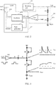
- FIG. 2 is a schematic diagram of the structure of a power module according to some embodiments of the present disclosure.
- the power module includes: a boosting unit 201, an enabling unit 202, and a control unit 203.
- the boosting unit 201 has a power output Vout for outputting a power supply voltage Vout.
- the boosting unit 201 includes a load capacitor, one end of the load capacitor serves as a power output Vout, and the load capacitor is charged to output a power supply voltage. When the output drops, the output voltage can be pulled up by supplementing energy to the load capacitor.
- the boosting unit 201 may be a charge pump circuit.
- FIG. 3 is a schematic diagram of the circuit structure of the boosting unit 201 according to some embodiments of the present disclosure.
- the boosting unit 201 includes an invertor INV, a capacitor C', a transistor M1 and a transistor M2, and a load capacitor C LOAD .
- the drain of the transistor M1 is connected to the power source Vcc
- the source of the transistor M1 is connected to the drain of the transistor M2
- the source of the transistor M2 is connected to the first terminal of the load capacitor C LOAD
- the second terminal of the load capacitor C LOAD is grounded.
- the gates of the transistor M1 and the transistor M2 are both connected to their respective drains.
- the input of the invertor INV is used to input the boost control signal CLK
- the output of the invertor INV is connected to the first terminal A of the capacitor C'
- the other end B of the capacitor C' is connected to the connecting terminal between the transistors M1 and M2.
- the capacitor C' is charged by the boost control signal CLK, thereby supplementing energy to the load capacitor C LOAD and increasing the power supply voltage output by the first terminal of the load capacitor C LOAD .
- the boosting unit 201 may also adopt a charge pump circuit of another structure, or adopt a boosting unit of another structure that can be controlled by a pulse signal.
- Those skilled in the art can reasonably select a suitable circuit structure as the boosting unit 201 according to the requirements of the output voltage of the power module.
- the enabling unit 202 is connected to the power output Vout for generating an enabling signal, and when the voltage of the power output Vout drops to a set value, the enabling signal generates a rising edge.
- the enabling unit 202 is configured to detect the voltage of the power output Vout.
- the enabling unit 202 includes a voltage divider circuit 2021 and a comparator CMP2.
- One end of the voltage divider circuit 2021 is connected to the power output Vout, and the other end of the voltage divider circuit 2021is grounded to GND1.
- the output of the voltage divider circuit 2021 is connected to the negative input of the comparator CMP2, and the positive input of the comparator CMP2 is connected to the reference voltage terminal, and the reference voltage value Vref2 is a set value.
- the voltage at the output of the voltage divider circuit 2021 varies with the voltage at the output voltage Vout of the power module, and preferably, is proportional to the voltage at the output Vout of the power module, and can accurately reflect amplitudes and changes of the output voltage of the output Vout of the power module.
- the voltage divider circuit 2021 includes a first voltage dividing resistor R11 and a second voltage dividing resistor R12, a first terminal of the first voltage dividing resistor R11 is connected to the power output Vout, and the second terminal of the first voltage dividing resistor R11 is connected to the first terminal of the second voltage dividing resistor R12, the second terminal of the second voltage dividing resistor R12 is grounded to GND1, the connecting terminal of the first voltage dividing resistor R11 and the second voltage dividing resistor R12 serves as the output of the voltage divider circuit 2021.
- the resistances of the first voltage dividing resistor R11 and the second voltage dividing resistor R12 can be selected rationally according to the requirement of the voltage division ratio.
- the voltage divider circuit 2021 may also have other circuit structures.
- the voltage divider circuit 2021 of the enabling unit 202 may also be another circuit structure capable of monitoring the output voltage Vout of the power module at any time.
- the oscillator 2031 is turned off.
- the power supply voltage Vout decreases, the voltage value of the voltage divider circuit 2021 output to the negative input of the comparator CMP2 is less than the reference voltage Vref2 of the positive input, then the enabling signal OSC_EN2 output by the comparator CMP2 generates a rising edge, which forms a high level signal, and triggers the oscillator 2031 to operate.
- the enabling unit 202 outputs an enabling signal OSC_EN2 corresponding to the voltage change of the output voltage Vout of the power module.
- the control unit 203 includes: an oscillator 2031, a pulse generator 2032, and an OR operation unit 2033.
- the input of the oscillator 2031 is connected to the output of the enabling unit 202.
- the oscillator 2031 is triggered by the enabling signal OSC_EN2 for generating a certain periodic delayed pulse control signal CLK2.
- the pulse generator 2032 is connected to the output of the enabling unit 202, and is configured to synchronously generate an instant pulse control signal one-shot while receiving the rising edge of the enabling signal OSC_EN2.
- the pulse generator 2032 is triggered by the rising edge of the enabling signal OSC_EN2 to generate the instant pulse control signal "one-shot" as a single pulse signal, that is, there has only one pulse.
- the “OR” operation unit 2033 is connected to the outputs of the oscillator 2031 and the pulse generator 2032, and performs "OR" calculation on the delayed pulse control signal CLK2 and the instant pulse control signal "one-shot” to generate the boost control signal CLK2'.
- the "OR" operation unit 2033 includes a NOR gate NOR1 and a NOT gate NOT1 connected in sequence, and two inputs of the NOR gate NOR1 are connected to the output of the pulse generator 2032 and the output of the oscillator 2031 respectively, the output of the NOR gate NOR1 is connected to the input of the NOT gate NOT1, and the output of the NOT gate NOT1 is connected to the input of the boosting unit 201 .
- the output of the control unit 203 is connected to the boosting unit 202 for outputting the boost control signal CLK2' to the boosting unit 202, and controlling the boosting unit 202 to increase the output voltage of the power module.
- FIG. 4 is a timing diagram of various signals in the power module in an embodiment of the present disclosure.
- the first pulse of the delayed pulse control signal CLK2 is later than the time instant that the enabling signal OSC_EN2 turns to a high level (that is, the rising edge moment), and the delay time is T.
- the pulse generator 2032 receives the high-level enabling signal OSC_EN2, it generates an instant pulse control signal "one-shot", and the rising edge of the instant pulse control signal one-shot is basically aligned with the rising edge of the enabling signal OSC _EN2 , both being generated at the same time or almost at the same time.
- the "OR” operation unit 2033 performs an “OR” operation on the delayed pulse control signal CLK2 and the instant pulse control signal "one-shot” to generate a boost control signal CLK2'.
- the boost control signal CLK2' is an instant pulse of the instant pulse control signal "one-shot", followed by the delayed pulse control signal CLK2.
- the power module of the present disclosure When detecting the voltage drop of the output voltage of Vout of the power module and the enabling signal OSC_EN2 turning into a high level, the power module of the present disclosure immediately generates a pulse of the boost control signal CLK2' to supplement the energy of the boosting unit 201 in time to increase the voltage at the output Vout of the power module, so that the output voltage is adjusted back to normal. Since the instant pulse control signal "one-shot" is generated immediately when the oscillator 2031 is enabled, and the output voltage Vout of the power module is supplied with energy via the boosting unit 201, the output voltage Vout does not need to wait for time T to obtain energy supplementation, and thus it can reduce the output voltage drop and prevent errors in subsequent circuits.
- the pulse generator 2032 includes a delay inversion circuit and an "AND” operation unit; the input of the delay inversion circuit is connected to the output of the enabling unit 202 for inverting the enabling signal and output the inverted enabling signal with a delay; the "AND” operation unit is connected to the output of the delay inversion circuit and the output of the enabling unit 202, and performs an "AND” calculation between the signal output by the delay inversion circuit and the enabling signal.
- FIG. 5a is a schematic structural diagram of a pulse generator according to an embodiment of the present disclosure.
- the pulse generator 2032 includes a delay inversion circuit 601 and an "AND" operation unit 602.
- the delay inversion circuit 601 includes: a first invertor INV1, a second invertor INV2, a third invertor INV3, a first capacitor C1 and a second capacitor C2.
- the input of the first invertor INV1 is connected to the output of the enabling unit 202, and the output of the first invertor INV1 is connected to the first terminal of the first capacitor C1 and to the input of the second invertor INV2.
- the output of the second invertor INV2 is connected to the first terminal of the second capacitor C2 and to the input of the third invertor INV3.
- the second terminals of the first capacitor C1 and the second capacitor C2 are all grounded.
- the output of the third invertor INV3 serves as the output of the delay inversion circuit 601.
- the "AND” operation unit 602 includes a NAND gate NAND1, and a gate NOT2 connected to the gate NAND1.
- the two inputs of the NAND gate NAND1 are connected to the output of the enabling unit 202 and the output of the delay inversion circuit 601 respectively.
- the output of the NAND gate NAND1 is connected to the input of the NOT gate NOT2, and the output of the NOT gate NOT2 serves as the output of the pulse generator 2032.
- the delay inversion circuit 601 includes a first capacitor C1 and a second capacitor C2.
- the enabling signal OSC _EN2 output from the enabling unit 202 turns high, it is necessary to charge the capacitors C1 and C2 first before outputting an inverted enabling signal OSC EN2, which means the enabling signal has a low level output to the "and" operation unit 602 after a delay. Therefore, the "AND" operation unit 602 performs an AND operation to the enabling signal OSC_EN2 and the delay inversion circuit 601, and outputs a high level for a certain period of time. After the delay inversion circuit 601 outputs a low level, the AND operation unit 602 outputs low level.
- the pulse generator 2032 generates a high level at the moment when OSC_EN2 changes to a high level and within a certain period of time, and then generate a low level, thereby forming an instant control pulse "one-shot".
- the pulse width of the real-time control pulse "one-shot” can be varied by adjusting the first capacitor C1 and the second capacitor C2, so as to avoid the energy supplement of the boosting unit 201 from being too small due to the pulse width being too small, or the energy supplement of the boosting unit 201 from being too large due to the pulse width being too wide, resulting in an overshoot of the output voltage.
- the pulse width of the "one-shot” can be adjusted to be close to or the same with the pulse width generated by the oscillator 203.
- FIG. 5b is a schematic structural diagram of a pulse generator according to another embodiment of the present disclosure.
- the delay inversion circuit 603 includes an invertor INV4, a resistor R', and a capacitor C3.
- the input of the invertor INV4 is connected to the output of the enabling unit 202, and the output of the invertor INV4 is connected to the first terminal of the resistor R', the second terminal of the resistor R' is connected to the first terminal of the capacitor C3, the second terminal of the capacitor C3 is grounded, and the first terminal of the capacitor C3 serves as the output of the delay inversion circuit 603.
- the delay inversion circuit 603 includes a capacitor C3.
- the capacitor C3 needs to be charged before the enabling signal OSC_EN2 can be inverted, which means, only after a period of delay, the low level output can be sent to the "AND" operation unit 602. Therefore, the "AND" operation unit 602 performs an AND operation between the enabling signal OSC_EN2 and the delay inversion circuit 603, and outputs a high level for a certain period of time, and the AND operation unit 602 outputs a low level only after the delay inversion circuit 603 outputs a low level.
- the pulse generator 2032 still generates a high level when a rising edge appears and then a high level lasts for a certain period of time for the enabling signal OSC_EN2, then changes to a low level, thereby generating an instant control pulse "one-shot".
- the charging time for the capacitor C3 can be adjusted by adjusting the size of the capacitor C3 and the size of the resistor R', thereby adjusting the pulse width of the "one-shot" instant pulse.
- the pulse generator 2032 or the delay inversion circuit 603 may also have other circuit structures as examples, which will not be described in details here. Those skilled in the art can reasonably choose proper circuit structures to implement the functions of the pulse generator 2032.
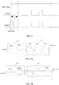
- FIG. 6 shows the timing sequence diagram illustrating the changes of the output voltage of the power module in an embodiment of the present disclosure and in the prior art.
- the load current I LOAD increases, which causes the output voltage Vout to decrease.
- Only the delayed pulse signal CLK2' output by the oscillator is used to supplement energy to the boosting unit 201 (referring to the FIG. 6 ) to increase the voltage at the output Vout of the power module. Since the delayed pulse signal CLK2' is generated after a period of delay since the output voltage Vout of the power module drops, the power supply voltage is decreased by ⁇ V1 and then increased gradually.
- a pulse signal is generated instantly in the pulse of the boost control signal CLK2' after Vout drops, so as to reduce the amount of voltage drop at the power output Vout.
- the voltage at the power output Vout is decreased by ⁇ V2 and then increased gradually, where ⁇ V2 ⁇ V1.
- the oscillator 203 will also generate a pulse signal with a larger clock interval to maintain the stability of the output voltage Vout.
- the power module of the above embodiments can instantly respond to the drop of the output voltage of the power module, and is able to adjust the output voltage back to a normal level, thereby improving the response speed of the power module.
- the specific implementation of the present disclosure also provides a memory, such as a DRAM memory, using the above-mentioned power module.
- the power module can be used to provide a word line driving voltage, bit line pre-charging voltage, in order to provide a stable power supply voltage to the memory.
- the memory chip frequently switches between various operation modes, the loads of the various module are changed, and when the load current is changed, the output voltage can be adjusted in time, to maintain a stable power supply voltage output, thereby improving the reliability and stability of the memory.
Landscapes
- Engineering & Computer Science (AREA)
- Power Engineering (AREA)
- Computer Hardware Design (AREA)
- Physics & Mathematics (AREA)
- Computing Systems (AREA)
- General Engineering & Computer Science (AREA)
- Mathematical Physics (AREA)
- Microelectronics & Electronic Packaging (AREA)
- Dc-Dc Converters (AREA)
Abstract
Description
- This application claims the benefit of priority to
Chinese Patent Application No.201910922840.6 filed on September 27, 2019 - The present disclosure relates to the field of integrated circuits, and in particular to a power module and a memory device.
- Various power modules, such as a charge pump, a linear regulator, etc. are needed in a Dynamic Random Access Memory (DRAM) chip, for powering different functional modules (such as word line drive voltage VPP, back gate bias voltage VBB, bit line pre-charge voltage VCC/2, etc.). During the operation process of the DRAM chip, various operation modes are frequently switched. In different operation modes, the current drawn by each functional module may be different from one another, which causes the output voltage of the power module to change. For example, in a low power consumption mode, when a heavy load suddenly occurs, the output voltage of the power module is pulled down quickly, and there is a certain delay for the voltage module to start voltage boost, during the time period of the delay, there is no extra energy to supply, meanwhile the output voltage of the voltage module continues to decrease, resulting in a large undershot of the output voltage, which affects the subsequent operations of other modules.
- Therefore, how to enhance the transient response of the power module has become a technical problem that needs to be solved urgently.
- The present disclosure provides a power module and a memory device to improve the transient response capability of the power module, thereby improving the stability of the memory device.
- To solve the above problem, the present disclosure provides a power module, which includes: a boosting unit, wherein the boosting unit has a power output for outputting a power supply voltage; an enabling unit, wherein the enabling unit is connected to the power output and is configured to generate an enabling signal, wherein a rising edge occurs in the enabling signal when the power supply voltage at the power output drops to a set value; a control unit, wherein the control unit comprises: an oscillator, a pulse generator and an "OR" operation unit; an oscillator, wherein the oscillator is connected to an output of the enabling unit, wherein the oscillator is configured to, when triggered by the rising edge of the enabling signal, generate a delayed pulse control signal with a certain period; a pulse generator, wherein the pulse generator is connected to the output of the enabling unit, and is configured to generate synchronously an instant pulse control signal at the same time when receiving the rising edge of the enabling signal; and an "OR" operation unit, wherein the "OR" operation unit is connected to an output of the oscillator and an output of the pulse generator, and wherein the "OR" operation unit is configured to perform an "OR" operation on the delayed pulse control signal and the instant pulse control signal to generate a boost control signal; wherein an output of the control unit is connected to the boosting unit, and the control unit is configured to output the boost control signal to the boosting unit to boost the power supply voltage.
- Optionally, the boosting unit is a charge pump circuit.
- Optionally, the enabling unit includes: a comparator and a voltage divider circuit, wherein a first terminal of the voltage divider circuit is connected to the power output, a second terminal of the boosting unit is grounded; and wherein an output of the voltage divider circuit is connected to a negative input of the comparator, a positive input of the comparator is connected to a reference voltage terminal, and a voltage value at the reference voltage terminal is a set value.
- Optionally, the voltage divider circuit includes: a first voltage dividing resistor and a second voltage dividing resistor, wherein a first terminal of the first voltage dividing resistor is connected to the power output, a second terminal of the first voltage dividing resistor is connected to a first terminal of the second voltage dividing resistor, a second terminal of the second voltage dividing resistor is grounded; and wherein a connecting terminal of the first voltage dividing resistor and the second voltage dividing resistor serves as an output of the voltage divider circuit.
- Optionally, the "OR" operation unit comprises a NOR gate and a NOT gate connected in sequence, wherein two inputs of the NOR gate are connected to the output of the pulse generator and the output of the oscillator respectively, wherein an output of the NOR gate is connected to an input of the NOT gate, and wherein an output of the NOT gate is connected to an input of the boosting unit.
- Optionally, the pulse generator comprises a delay inversion circuit and an "AND" operation unit; wherein an input of the delay inversion circuit is connected to the output of the enabling unit, and is configured to invert the enabling signal and output the inverted enabling signal with a delay; wherein the "AND" operation unit is connected to the output of the delay inversion circuit and the output of the enabling unit, and is configured to perform an "AND" operation on the signal from the delay inversion circuit and the enabling signal.
- Optionally, the delay inversion circuit comprises: a first invertor, a resistor and a capacitor, wherein an input of the first invertor is connected to the output of the enabling unit, an output of the first invertor is connected to a first terminal of the resistor, a second terminal of the resistor is connected to a first terminal of the capacitor, and a second terminal of the capacitor is grounded, and wherein the first terminal of the capacitor serves as the output of the delay inversion circuit.
- Optionally, the delay inversion circuit comprises: a first invertor, a second invertor, a third invertor, a first capacitor, and a second capacitor; wherein an input of the first invertor is connected to the output of the enabling unit, an output of the first invertor is connected to a first terminal of the first capacitor and a first terminal of the second invertor; wherein an output of the second invertor is connected to a first terminal of the second capacitor and an input of the third invertor; wherein second terminals of the first capacitor and the second capacitor are grounded; and wherein an output of the third invertor is used as the output of the delay inversion circuit.
- Optionally, the "AND" operation unit includes a NAND gate and a NOT gate connected to the NAND gate.
- Optionally, the first rising edge of the instant pulse control signal and the rising edge of the enabling signal are generated simultaneously.
- The present disclosure also provides a memory device with a power module. The power module includes: a boosting unit, wherein the boosting unit has a power output for outputting a power supply voltage; an enabling unit, wherein the enabling unit is connected to the power output and is configured to generate an enabling signal, wherein a rising edge occurs in the enabling signal when the power supply voltage at the power output drops to a set value; a control unit, wherein the control unit comprises: an oscillator, a pulse generator and an "OR" operation unit; an oscillator, wherein the oscillator is connected to an output of the enabling unit, wherein the oscillator is configured to, when triggered by the rising edge of the enabling signal, generate a delayed pulse control signal with a certain period; a pulse generator, wherein the pulse generator is connected to the output of the enabling unit, and is configured to generate synchronously an instant pulse control signal at the same time when receiving the rising edge of the enabling signal; and an "OR" operation unit, wherein the "OR" operation unit is connected to an output of the oscillator and an output of the pulse generator, and wherein the "OR" operation unit is configured to perform an "OR" operation on the delayed pulse control signal and the instant pulse control signal to generate a boost control signal; wherein an output of the control unit is connected to the boosting unit, and the control unit is configured to output the boost control signal to the boosting unit to boost the power supply voltage.
- Optionally, the boosting unit is a charge pump circuit.
- Optionally, the enabling unit includes: a comparator and a voltage divider circuit, wherein a first terminal of the voltage divider circuit is connected to the power output, a second terminal of the boosting unit is grounded; and wherein an output of the voltage divider circuit is connected to a negative input of the comparator, a positive input of the comparator is connected to a reference voltage terminal, and a voltage value at the reference voltage terminal is a set value.
- Optionally, the voltage divider circuit includes: a first voltage dividing resistor and a second voltage dividing resistor, wherein a first terminal of the first voltage dividing resistor is connected to the power output, a second terminal of the first voltage dividing resistor is connected to a first terminal of the second voltage dividing resistor, a second terminal of the second voltage dividing resistor is grounded; and wherein a connecting terminal of the first voltage dividing resistor and the second voltage dividing resistor serves as an output of the voltage divider circuit.
- Optionally, the "OR" operation unit comprises a NOR gate and a NOT gate connected in sequence, wherein two inputs of the NOR gate are connected to the output of the pulse generator and the output of the oscillator respectively, wherein an output of the NOR gate is connected to an input of the NOT gate, and wherein an output of the NOT gate is connected to an input of the boosting unit.
- Optionally, the pulse generator includes a delay inversion circuit and an "AND" operation unit; wherein an input of the delay inversion circuit is connected to the output of the enabling unit, and is configured to invert the enabling signal and output the inverted enabling signal with a delay; wherein the "AND" operation unit is connected to the output of the delay inversion circuit and the output of the enabling unit, and is configured to perform an "AND" operation on the signal from the delay inversion circuit and the enabling signal.
- Optionally, the delay inversion circuit includes: a first invertor, a resistor and a capacitor, wherein an input of the first invertor is connected to the output of the enabling unit, an output of the first invertor is connected to a first terminal of the resistor, a second terminal of the resistor is connected to a first terminal of the capacitor, and a second terminal of the capacitor is grounded, and wherein the first terminal of the capacitor serves as the output of the delay inversion circuit.
- Optionally, the delay inversion circuit includes: a first invertor, a second invertor, a third invertor, a first capacitor, and a second capacitor; wherein an input of the first invertor is connected to the output of the enabling unit, an output of the first invertor is connected to a first terminal of the first capacitor and a first terminal of the second invertor; wherein an output of the second invertor is connected to a first terminal of the second capacitor and an input of the third invertor; wherein second terminals of the first capacitor and the second capacitor are grounded; and wherein an output of the third invertor is used as the output of the delay inversion circuit.
- Optionally, the "AND" operation unit includes a NAND gate and a NOT gate connected to the NAND gate.
- Optionally, the first rising edge of the instant pulse control signal and the rising edge of the enabling signal are generated simultaneously.
- The power module of the present disclosure can supplement energy to the boosting unit in time after detecting the voltage drop at the output of the power supply, and adjust the output back to the normal voltage, so that the output of the power supply can be supplemented with energy without waiting. Thereby, the output voltage drop is reduced and errors in subsequent circuits are prevented.
- By describing its exemplary embodiments in detail with reference to the accompanying drawings, the above and other objectives, features and advantages of the present disclosure will become more apparent.
-
FIG. 1a is a schematic diagram of the structure of a power module in the prior art; -
FIG. 1b is a schematic time sequence of various signals of the power module in the prior art; -
FIG. 2 is a schematic diagram of the structure of a power module according to some embodiments of the present disclosure; -
FIG. 3 is a schematic diagram of a boosting unit of a power module according to some embodiments of the present disclosure; -
FIG. 4 is a schematic timing diagram of various signals in the power module in some embodiments of the present disclosure; -
FIG. 5a is a schematic diagram of the circuit structure of a pulse generator of a power module according to some embodiments of the present disclosure; -
FIG. 5b is a schematic diagram of the circuit structure of a pulse generator of a power module according to some embodiments of the present disclosure; and -
FIG. 6 is the timing diagram illustrating changes of the output voltage of the power module in an embodiment of the present disclosure and in the prior art. - Listed below are definitions of various reference numbers in
FIGs. 1-6 : - 101 oscillator;
- 102 charge pump circuit;
- 201 boosting unit;
- 202 enabling unit;
- 2021 voltage divider circuit;
- 203 control unit;
- 2031 oscillator;
- 2032 pulse generator;
- 2033 "or" operation unit;
- 601 delay inversion Circuit;
- 602 "and" operation unit;
- Vout power output;
- R1 resistor;
- R2 resistor;
- R' resistor;
- CMP1 comparator;
- CMP2 comparator;
- Vref reference voltage;
- OSC_EN enabling signal;
- OSC_EN2 enabling signal;
- CLK boost control Signal;
- CLK2' boost control signal;
- T_delay delay;
- T delay time;
- INV invertor;
- INV4 invertor;
- C' capacitor;
- C3 capacitor;
- M1 transistor;
- M2 transistor;
- CLOAD load capacitor;
- Vcc power supply;
- R11 first voltage division resistor;
- R12 second voltage division resistor;
- Vref2 reference voltage;
- CLK2 delayed pulse control signal;
- one-shot instant pulse control signal;
- NOR1 NOR gate;
- NOT1 NOT gate;
- NOT2 NOT gate;
- INV1 first invertor;
- INV2 Second invertor;
- INV3 third invertor;
- C1 first capacitor;
- C2 second capacitor;
- NAND1 NAND gate;
- NOT2 invertor; and
- ILOAD load current.
- As described in the background art, the response of an existing power module is relatively slow, which often leads to the problem of unstable output voltage.
- Please refer to
FIG. 1a , which is a schematic diagram of the structure of a power module in the prior art. - The power module includes: a
charge pump circuit 102, a power output Vout is configured to output a power supply voltage to the load, the power output Vout is connected to a resistor R1 and a resistor R2 connected in series to the ground, and the resistor R1 and the resistor R2 form a voltage divider circuit, the connection node of the resistor R1 and the resistor R2 is connected to the negative input of the comparator CMP1, the positive input of the comparator CMP1 is connected to the reference voltage Vref, and the output of the comparator CMP1 is connected to theoscillator 101, is further connected to thecharge pump circuit 102 through the output of theoscillator 101. - In the low power consumption mode, the input voltage of the negative input of the comparator CMP1 is greater than the reference voltage Vref, and the output enabling signal OSC_EN of the comparator CMP1 is low. At this time, the
oscillator 101 is turned off to save power. In this mode, if the load on the power output Vout suddenly becomes heavy, the output power supply voltage Vout is pulled down quickly, the output enabling signal OSC_EN of the comparator CMP1 is at high level, and theoscillator 101 is enabled. Theoscillator 101 is enabled in response to receiving the enabling signal OSC_EN, and there is a delay T_delay (please refer toFigure 1b ) from the time when the enabling signal OSC EN is received to the time when a pulse signal CLK is output. During the time period of the delay, no energy is supplied to the output capacitor of thecharge pump circuit 102, so the output voltage Vout continues to drop, resulting in a large drop in the output voltage Vout, which affects the stability of the subsequent modules. - It can be seen that reducing the pulse delay of the boost control signal CLK for controlling the boost of the
charge pump circuit 102 can reduce the drop of the output voltage Vout, and produce energy to thecharge pump circuit 102 in time to stabilize the output power supply voltage. - Based on this, a new power module is proposed, which can respond quickly when the load suddenly becomes heavy, to reduce the drop of the output voltage.
-
FIG. 2 is a schematic diagram of the structure of a power module according to some embodiments of the present disclosure. - In this embodiment, the power module includes: a boosting
unit 201, an enablingunit 202, and acontrol unit 203. - The boosting
unit 201 has a power output Vout for outputting a power supply voltage Vout. - The boosting
unit 201 includes a load capacitor, one end of the load capacitor serves as a power output Vout, and the load capacitor is charged to output a power supply voltage. When the output drops, the output voltage can be pulled up by supplementing energy to the load capacitor. In an embodiment of the present disclosure, the boostingunit 201 may be a charge pump circuit. -
FIG. 3 is a schematic diagram of the circuit structure of the boostingunit 201 according to some embodiments of the present disclosure. - In this embodiment, the boosting
unit 201 includes an invertor INV, a capacitor C', a transistor M1 and a transistor M2, and a load capacitor CLOAD. The drain of the transistor M1 is connected to the power source Vcc, the source of the transistor M1 is connected to the drain of the transistor M2, the source of the transistor M2 is connected to the first terminal of the load capacitor CLOAD, and the second terminal of the load capacitor CLOAD is grounded. The gates of the transistor M1 and the transistor M2 are both connected to their respective drains. The input of the invertor INV is used to input the boost control signal CLK, the output of the invertor INV is connected to the first terminal A of the capacitor C', and the other end B of the capacitor C' is connected to the connecting terminal between the transistors M1 and M2. The capacitor C' is charged by the boost control signal CLK, thereby supplementing energy to the load capacitor CLOAD and increasing the power supply voltage output by the first terminal of the load capacitor CLOAD. - In other embodiments, the boosting
unit 201 may also adopt a charge pump circuit of another structure, or adopt a boosting unit of another structure that can be controlled by a pulse signal. Those skilled in the art can reasonably select a suitable circuit structure as the boostingunit 201 according to the requirements of the output voltage of the power module. - The enabling
unit 202 is connected to the power output Vout for generating an enabling signal, and when the voltage of the power output Vout drops to a set value, the enabling signal generates a rising edge. The enablingunit 202 is configured to detect the voltage of the power output Vout. - In this implementation, the enabling
unit 202 includes avoltage divider circuit 2021 and a comparator CMP2. One end of thevoltage divider circuit 2021 is connected to the power output Vout, and the other end of the voltage divider circuit 2021is grounded to GND1. The output of thevoltage divider circuit 2021 is connected to the negative input of the comparator CMP2, and the positive input of the comparator CMP2 is connected to the reference voltage terminal, and the reference voltage value Vref2 is a set value. - The voltage at the output of the
voltage divider circuit 2021 varies with the voltage at the output voltage Vout of the power module, and preferably, is proportional to the voltage at the output Vout of the power module, and can accurately reflect amplitudes and changes of the output voltage of the output Vout of the power module. In this embodiment, thevoltage divider circuit 2021 includes a first voltage dividing resistor R11 and a second voltage dividing resistor R12, a first terminal of the first voltage dividing resistor R11 is connected to the power output Vout, and the second terminal of the first voltage dividing resistor R11 is connected to the first terminal of the second voltage dividing resistor R12, the second terminal of the second voltage dividing resistor R12 is grounded to GND1, the connecting terminal of the first voltage dividing resistor R11 and the second voltage dividing resistor R12 serves as the output of thevoltage divider circuit 2021. The resistances of the first voltage dividing resistor R11 and the second voltage dividing resistor R12 can be selected rationally according to the requirement of the voltage division ratio. In other implementations, thevoltage divider circuit 2021 may also have other circuit structures. In other embodiments, thevoltage divider circuit 2021 of the enablingunit 202 may also be another circuit structure capable of monitoring the output voltage Vout of the power module at any time. - When the output voltage Vout of the power module is high, the voltage value output by the
voltage divider circuit 2021 to the negative input of the comparator CMP2 is greater than the reference voltage Vref2 at the positive input of the comparator CMP2, and the enabling signal OSC_EN2 output by the comparator CMP2 is low, theoscillator 2031 is turned off. When the power supply voltage Vout decreases, the voltage value of thevoltage divider circuit 2021 output to the negative input of the comparator CMP2 is less than the reference voltage Vref2 of the positive input, then the enabling signal OSC_EN2 output by the comparator CMP2 generates a rising edge, which forms a high level signal, and triggers theoscillator 2031 to operate. - The enabling
unit 202 outputs an enabling signal OSC_EN2 corresponding to the voltage change of the output voltage Vout of the power module. - The
control unit 203 includes: anoscillator 2031, apulse generator 2032, and anOR operation unit 2033. - The input of the
oscillator 2031 is connected to the output of the enablingunit 202. When the enabling signal OSC_EN2 is at a high level, theoscillator 2031 is triggered by the enabling signal OSC_EN2 for generating a certain periodic delayed pulse control signal CLK2. - The
pulse generator 2032 is connected to the output of the enablingunit 202, and is configured to synchronously generate an instant pulse control signal one-shot while receiving the rising edge of the enabling signal OSC_EN2. In this specific embodiment, thepulse generator 2032 is triggered by the rising edge of the enabling signal OSC_EN2 to generate the instant pulse control signal "one-shot" as a single pulse signal, that is, there has only one pulse. - The "OR"
operation unit 2033 is connected to the outputs of theoscillator 2031 and thepulse generator 2032, and performs "OR" calculation on the delayed pulse control signal CLK2 and the instant pulse control signal "one-shot" to generate the boost control signal CLK2'. - In this implementation, the "OR"
operation unit 2033 includes a NOR gate NOR1 and a NOT gate NOT1 connected in sequence, and two inputs of the NOR gate NOR1 are connected to the output of thepulse generator 2032 and the output of theoscillator 2031 respectively, the output of the NOR gate NOR1 is connected to the input of the NOT gate NOT1, and the output of the NOT gate NOT1 is connected to the input of the boostingunit 201 . - The output of the
control unit 203 is connected to the boostingunit 202 for outputting the boost control signal CLK2' to the boostingunit 202, and controlling the boostingunit 202 to increase the output voltage of the power module. -
FIG. 4 is a timing diagram of various signals in the power module in an embodiment of the present disclosure. - In this embodiment, when the load of the power output Vout becomes heavy, the output voltage decreases, so that the enabling signal OSC_EN2 becomes a high level, so that the
oscillator 2031 is enabled and outputs a delayed pulse control signal CLK2. Because of the circuit characteristics of theoscillator 2031, the first pulse of the delayed pulse control signal CLK2 is later than the time instant that the enabling signal OSC_EN2 turns to a high level (that is, the rising edge moment), and the delay time is T. - Once the
pulse generator 2032 receives the high-level enabling signal OSC_EN2, it generates an instant pulse control signal "one-shot", and the rising edge of the instant pulse control signal one-shot is basically aligned with the rising edge of the enabling signal OSC _EN2 , both being generated at the same time or almost at the same time. - The "OR"
operation unit 2033 performs an "OR" operation on the delayed pulse control signal CLK2 and the instant pulse control signal "one-shot" to generate a boost control signal CLK2'. Within the delay time T, the boost control signal CLK2' is an instant pulse of the instant pulse control signal "one-shot", followed by the delayed pulse control signal CLK2. - When detecting the voltage drop of the output voltage of Vout of the power module and the enabling signal OSC_EN2 turning into a high level, the power module of the present disclosure immediately generates a pulse of the boost control signal CLK2' to supplement the energy of the boosting
unit 201 in time to increase the voltage at the output Vout of the power module, so that the output voltage is adjusted back to normal. Since the instant pulse control signal "one-shot" is generated immediately when theoscillator 2031 is enabled, and the output voltage Vout of the power module is supplied with energy via the boostingunit 201, the output voltage Vout does not need to wait for time T to obtain energy supplementation, and thus it can reduce the output voltage drop and prevent errors in subsequent circuits. - The
pulse generator 2032 includes a delay inversion circuit and an "AND" operation unit; the input of the delay inversion circuit is connected to the output of the enablingunit 202 for inverting the enabling signal and output the inverted enabling signal with a delay; the "AND" operation unit is connected to the output of the delay inversion circuit and the output of the enablingunit 202, and performs an "AND" calculation between the signal output by the delay inversion circuit and the enabling signal. -
FIG. 5a is a schematic structural diagram of a pulse generator according to an embodiment of the present disclosure. - The
pulse generator 2032 includes adelay inversion circuit 601 and an "AND"operation unit 602. - The
delay inversion circuit 601 includes: a first invertor INV1, a second invertor INV2, a third invertor INV3, a first capacitor C1 and a second capacitor C2. The input of the first invertor INV1 is connected to the output of the enablingunit 202, and the output of the first invertor INV1 is connected to the first terminal of the first capacitor C1 and to the input of the second invertor INV2. The output of the second invertor INV2 is connected to the first terminal of the second capacitor C2 and to the input of the third invertor INV3. The second terminals of the first capacitor C1 and the second capacitor C2 are all grounded. The output of the third invertor INV3 serves as the output of thedelay inversion circuit 601. - The "AND"
operation unit 602 includes a NAND gate NAND1, and a gate NOT2 connected to the gate NAND1. The two inputs of the NAND gate NAND1 are connected to the output of the enablingunit 202 and the output of thedelay inversion circuit 601 respectively. The output of the NAND gate NAND1 is connected to the input of the NOT gate NOT2, and the output of the NOT gate NOT2 serves as the output of thepulse generator 2032. - The
delay inversion circuit 601 includes a first capacitor C1 and a second capacitor C2. When the enabling signal OSC _EN2 output from the enablingunit 202 turns high, it is necessary to charge the capacitors C1 and C2 first before outputting an inverted enabling signal OSC EN2, which means the enabling signal has a low level output to the "and"operation unit 602 after a delay. Therefore, the "AND"operation unit 602 performs an AND operation to the enabling signal OSC_EN2 and thedelay inversion circuit 601, and outputs a high level for a certain period of time. After thedelay inversion circuit 601 outputs a low level, the ANDoperation unit 602 outputs low level. Therefore, thepulse generator 2032 generates a high level at the moment when OSC_EN2 changes to a high level and within a certain period of time, and then generate a low level, thereby forming an instant control pulse "one-shot". The pulse width of the real-time control pulse "one-shot" can be varied by adjusting the first capacitor C1 and the second capacitor C2, so as to avoid the energy supplement of the boostingunit 201 from being too small due to the pulse width being too small, or the energy supplement of the boostingunit 201 from being too large due to the pulse width being too wide, resulting in an overshoot of the output voltage. Preferably, the pulse width of the "one-shot" can be adjusted to be close to or the same with the pulse width generated by theoscillator 203. -
FIG. 5b is a schematic structural diagram of a pulse generator according to another embodiment of the present disclosure. - In this embodiment, another circuit structure of the
delay inversion circuit 603 is provided. Thedelay inversion circuit 603 includes an invertor INV4, a resistor R', and a capacitor C3. The input of the invertor INV4 is connected to the output of the enablingunit 202, and the output of the invertor INV4 is connected to the first terminal of the resistor R', the second terminal of the resistor R' is connected to the first terminal of the capacitor C3, the second terminal of the capacitor C3 is grounded, and the first terminal of the capacitor C3 serves as the output of thedelay inversion circuit 603. - The
delay inversion circuit 603 includes a capacitor C3. When the enabling signal OSC_EN2 output from the enablingunit 202 changes to a high level, the capacitor C3 needs to be charged before the enabling signal OSC_EN2 can be inverted, which means, only after a period of delay, the low level output can be sent to the "AND"operation unit 602. Therefore, the "AND"operation unit 602 performs an AND operation between the enabling signal OSC_EN2 and thedelay inversion circuit 603, and outputs a high level for a certain period of time, and the ANDoperation unit 602 outputs a low level only after thedelay inversion circuit 603 outputs a low level. Therefore, thepulse generator 2032 still generates a high level when a rising edge appears and then a high level lasts for a certain period of time for the enabling signal OSC_EN2, then changes to a low level, thereby generating an instant control pulse "one-shot". - In this embodiment, the charging time for the capacitor C3 can be adjusted by adjusting the size of the capacitor C3 and the size of the resistor R', thereby adjusting the pulse width of the "one-shot" instant pulse.
- In another embodiment of the present disclosure, the
pulse generator 2032 or thedelay inversion circuit 603 may also have other circuit structures as examples, which will not be described in details here. Those skilled in the art can reasonably choose proper circuit structures to implement the functions of thepulse generator 2032. -
FIG. 6 shows the timing sequence diagram illustrating the changes of the output voltage of the power module in an embodiment of the present disclosure and in the prior art. - In the prior art, when in a heavy load state, the load current ILOAD increases, which causes the output voltage Vout to decrease. Only the delayed pulse signal CLK2' output by the oscillator is used to supplement energy to the boosting unit 201 (referring to the
FIG. 6 ) to increase the voltage at the output Vout of the power module. Since the delayed pulse signal CLK2' is generated after a period of delay since the output voltage Vout of the power module drops, the power supply voltage is decreased by ΔV1 and then increased gradually. - In the embodiment of the present disclosure, a pulse signal is generated instantly in the pulse of the boost control signal CLK2' after Vout drops, so as to reduce the amount of voltage drop at the power output Vout. The voltage at the power output Vout is decreased by ΔV2 and then increased gradually, where ΔV2<ΔV1.
- Here, the power module is in the light load and low power consumption mode, the
oscillator 203 will also generate a pulse signal with a larger clock interval to maintain the stability of the output voltage Vout. - The power module of the above embodiments can instantly respond to the drop of the output voltage of the power module, and is able to adjust the output voltage back to a normal level, thereby improving the response speed of the power module.
- The specific implementation of the present disclosure also provides a memory, such as a DRAM memory, using the above-mentioned power module. The power module can be used to provide a word line driving voltage, bit line pre-charging voltage, in order to provide a stable power supply voltage to the memory. During the operation process of the memory chip, the memory chip frequently switches between various operation modes, the loads of the various module are changed, and when the load current is changed, the output voltage can be adjusted in time, to maintain a stable power supply voltage output, thereby improving the reliability and stability of the memory.
- The above are only the preferred embodiments of the present disclosure. It should be pointed out that for those of ordinary skill in the art, without departing from the principle of the present disclosure, many improvements and modifications can be made, and these improvements and modifications should also be considered as within the protection scope of the invention.
Claims (20)
- A power module, comprising:a boosting unit, wherein the boosting unit has a power output for outputting a power supply voltage;an enabling unit, wherein the enabling unit is connected to the power output and is configured to generate an enabling signal, wherein a rising edge occurs in the enabling signal when the power supply voltage at the power output drops to a set value;a control unit, wherein the control unit comprises: an oscillator, a pulse generator and an "OR" operation unit;an oscillator, wherein the oscillator is connected to an output of the enabling unit, wherein the oscillator is configured to, when triggered by the rising edge of the enabling signal, generate a delayed pulse control signal with a certain period;a pulse generator, wherein the pulse generator is connected to the output of the enabling unit, and is configured to generate synchronously an instant pulse control signal at the same time when receiving the rising edge of the enabling signal; andan "OR" operation unit, wherein the "OR" operation unit is connected to an output of the oscillator and an output of the pulse generator, and wherein the "OR" operation unit is configured to perform an "OR" operation on the delayed pulse control signal and the instant pulse control signal to generate a boost control signal;wherein an output of the control unit is connected to the boosting unit, and the control unit is configured to output the boost control signal to the boosting unit to boost the power supply voltage.
- The power module according to claim 1, wherein the boosting unit is a charge pump circuit.
- The power module according to claim 1, wherein the enabling unit further comprises: a comparator and a voltage divider circuit, wherein a first terminal of the voltage divider circuit is connected to the power output, a second terminal of the boosting unit is grounded; and wherein an output of the voltage divider circuit is connected to a negative input of the comparator, a positive input of the comparator is connected to a reference voltage terminal, and a voltage value at the reference voltage terminal is a set value.
- The power module according to claim 3, wherein the voltage divider circuit further comprises: a first voltage dividing resistor and a second voltage dividing resistor, wherein a first terminal of the first voltage dividing resistor is connected to the power output, a second terminal of the first voltage dividing resistor is connected to a first terminal of the second voltage dividing resistor, a second terminal of the second voltage dividing resistor is grounded; and wherein a connecting terminal of the first voltage dividing resistor and the second voltage dividing resistor serves as an output of the voltage divider circuit.
- The power module according to claim 1, wherein the "OR" operation unit comprises a NOR gate and a NOT gate connected in sequence, wherein two inputs of the NOR gate are connected to the output of the pulse generator and the output of the oscillator respectively, wherein an output of the NOR gate is connected to an input of the NOT gate, and wherein an output of the NOT gate is connected to an input of the boosting unit.
- The power module according to claim 1, wherein the pulse generator comprises a delay inversion circuit and an "AND" operation unit; wherein an input of the delay inversion circuit is connected to the output of the enabling unit, and is configured to invert the enabling signal and output the inverted enabling signal with a delay; wherein the "AND" operation unit is connected to the output of the delay inversion circuit and the output of the enabling unit, and is configured to perform an "AND" operation on the signal from the delay inversion circuit and the enabling signal.
- The power module according to claim 6, wherein the delay inversion circuit comprises: a first invertor, a resistor and a capacitor, wherein an input of the first invertor is connected to the output of the enabling unit, an output of the first invertor is connected to a first terminal of the resistor, a second terminal of the resistor is connected to a first terminal of the capacitor, and a second terminal of the capacitor is grounded, and wherein the first terminal of the capacitor serves as the output of the delay inversion circuit.
- The power module according to claim 6, wherein the delay inversion circuit comprises: a first invertor, a second invertor, a third invertor, a first capacitor, and a second capacitor; wherein an input of the first invertor is connected to the output of the enabling unit, an output of the first invertor is connected to a first terminal of the first capacitor and a first terminal of the second invertor; wherein an output of the second invertor is connected to a first terminal of the second capacitor and an input of the third invertor; wherein second terminals of the first capacitor and the second capacitor are grounded; and wherein an output of the third invertor is used as the output of the delay inversion circuit.
- The power module according to claim 6, wherein the "AND" operation unit comprises a NAND gate and a NOT gate connected to the NAND gate.
- The power module according to claim 6, wherein a first rising edge of the instant pulse control signal and the rising edge of the enabling signal are generated simultaneously.
- A memory device, comprising a power module, wherein the power module comprises:a boosting unit, wherein the boosting unit has a power output for outputting a power supply voltage;an enabling unit, wherein the enabling unit is connected to the power output and is configured to generate an enabling signal, wherein a rising edge occurs in the enabling signal when the power supply voltage at the power output drops to a set value;a control unit, wherein the control unit comprises: an oscillator, a pulse generator and an "OR" operation unit;an oscillator, wherein the oscillator is connected to an output of the enabling unit, wherein the oscillator is configured to, when triggered by the rising edge of the enabling signal, generate a delayed pulse control signal with a certain period;a pulse generator, wherein the pulse generator is connected to the output of the enabling unit, and is configured to generate synchronously an instant pulse control signal at the same time when receiving the rising edge of the enabling signal; andan "OR" operation unit, wherein the "OR" operation unit is connected to an output of the oscillator and an output of the pulse generator, and wherein the "OR" operation unit is configured to perform an "OR" operation on the delayed pulse control signal and the instant pulse control signal to generate a boost control signal;
wherein an output of the control unit is connected to the boosting unit, and the control unit is configured to output the boost control signal to the boosting unit to boost the power supply voltage. - The memory device of claim 11, wherein the boosting unit is a charge pump circuit.
- The memory device according to claim 11, wherein the enabling unit further comprises: a comparator and a voltage divider circuit, wherein a first terminal of the voltage divider circuit is connected to the power output, a second terminal of the boosting unit is grounded; and wherein an output of the voltage divider circuit is connected to a negative input of the comparator, a positive input of the comparator is connected to a reference voltage terminal, and a voltage value at the reference voltage terminal is a set value.
- The memory device according to claim 13, wherein the voltage divider circuit further comprises: a first voltage dividing resistor and a second voltage dividing resistor, wherein a first terminal of the first voltage dividing resistor is connected to the power output, a second terminal of the first voltage dividing resistor is connected to a first terminal of the second voltage dividing resistor, a second terminal of the second voltage dividing resistor is grounded; and wherein a connecting terminal of the first voltage dividing resistor and the second voltage dividing resistor serves as an output of the voltage divider circuit.
- The memory device according to claim 11, wherein the "OR" operation unit comprises a NOR gate and a NOT gate connected in sequence, wherein two inputs of the NOR gate are connected to the output of the pulse generator and the output of the oscillator respectively, wherein an output of the NOR gate is connected to an input of the NOT gate, and wherein an output of the NOT gate is connected to an input of the boosting unit.
- The memory device according to claim 11, wherein the pulse generator comprises a delay inversion circuit and an "AND" operation unit; wherein an input of the delay inversion circuit is connected to the output of the enabling unit, and is configured to invert the enabling signal and output the inverted enabling signal with a delay; wherein the "AND" operation unit is connected to the output of the delay inversion circuit and the output of the enabling unit, and is configured to perform an "AND" operation on the signal from the delay inversion circuit and the enabling signal.
- The memory device according to claim 16, wherein the delay inversion circuit comprises:a first invertor, a resistor and a capacitor, wherein an input of the first invertor is connected to the output of the enabling unit, an output of the first invertor is connected to a first terminal of the resistor, a second terminal of the resistor is connected to a first terminal of the capacitor,and a second terminal of the capacitor is grounded, and wherein the first terminal of the capacitor serves as the output of the delay inversion circuit.
- The memory device according to claim 16, wherein the delay inversion circuit comprises:a first invertor, a second invertor, a third invertor, a first capacitor, and a second capacitor;wherein an input of the first invertor is connected to the output of the enabling unit, an output of the first invertor is connected to a first terminal of the first capacitor and a first terminal of the second invertor; wherein an output of the second invertor is connected to a first terminal of the second capacitor and an input of the third invertor; wherein second terminals of the first capacitor and the second capacitor are grounded; and wherein an output of the third invertor is used as the output of the delay inversion circuit.
- The memory device according to claim 16, wherein the "AND" operation unit comprises a NAND gate and a NOT gate connected to the NAND gate.
- The memory device of claim 16, wherein a first rising edge of the instant pulse control signal and the rising edge of the enabling signal are generated simultaneously.
Applications Claiming Priority (2)
| Application Number | Priority Date | Filing Date | Title |
|---|---|---|---|
| CN201910922840.6A CN112583259B (en) | 2019-09-27 | 2019-09-27 | Power module and memory |
| PCT/CN2020/076310 WO2021056957A1 (en) | 2019-09-27 | 2020-02-22 | Power supply module, and memory device |
Publications (3)
| Publication Number | Publication Date |
|---|---|
| EP3896832A1 true EP3896832A1 (en) | 2021-10-20 |
| EP3896832A4 EP3896832A4 (en) | 2022-04-06 |
| EP3896832B1 EP3896832B1 (en) | 2023-06-14 |
Family
ID=75109946
Family Applications (1)
| Application Number | Title | Priority Date | Filing Date |
|---|---|---|---|
| EP20869411.7A Active EP3896832B1 (en) | 2019-09-27 | 2020-02-22 | Power supply module, and memory device |
Country Status (4)
| Country | Link |
|---|---|
| US (1) | US11393521B2 (en) |
| EP (1) | EP3896832B1 (en) |
| CN (1) | CN112583259B (en) |
| WO (1) | WO2021056957A1 (en) |
Families Citing this family (2)
| Publication number | Priority date | Publication date | Assignee | Title |
|---|---|---|---|---|
| US10534386B2 (en) * | 2016-11-29 | 2020-01-14 | Taiwan Semiconductor Manufacturing Co., Ltd. | Low-dropout voltage regulator circuit |
| US12040705B2 (en) * | 2021-08-20 | 2024-07-16 | Semiconductor Components Industries, Llc | Self clocked low power doubling charge pump |
Family Cites Families (24)
| Publication number | Priority date | Publication date | Assignee | Title |
|---|---|---|---|---|
| US4578599A (en) * | 1983-06-02 | 1986-03-25 | Motorola, Inc. | Flip-flop having improved synchronous reset |
| US5134315A (en) * | 1991-02-07 | 1992-07-28 | National Semiconductor Corporation | Synchronous counter terminal count output circuit |
| CN2106641U (en) | 1991-12-05 | 1992-06-10 | 朱金龙 | Luminous means mounted to the mechanical power toy |
| KR950013342B1 (en) | 1992-10-06 | 1995-11-02 | 삼성전자주식회사 | Fault Relief Circuit in Semiconductor Memory Device |
| JPH09288897A (en) * | 1996-04-19 | 1997-11-04 | Sony Corp | Voltage supply circuit |
| KR100256819B1 (en) | 1997-06-30 | 2000-05-15 | 김영환 | Synchronous DRAM stabilizes redundant operation |
| JP2001184890A (en) | 1999-12-27 | 2001-07-06 | Mitsubishi Electric Corp | Semiconductor storage device |
| US6979987B2 (en) * | 2002-11-14 | 2005-12-27 | Fyre Storm, Inc. | Method of regulating an output voltage of a power converter by sensing the output voltage during a first time interval and calculating a next current value in an inductor sufficient to bring the output voltage to a target voltage within a second time interval immediately following the first time interval and varying a duty cycle of a switch during the second time interval |
| KR100680441B1 (en) * | 2005-06-07 | 2007-02-08 | 주식회사 하이닉스반도체 | Step-up Voltage Generator Generates Stable Step-Up Voltage |
| JP4728777B2 (en) * | 2005-11-02 | 2011-07-20 | 株式会社東芝 | Power circuit |
| KR100861371B1 (en) * | 2007-06-25 | 2008-10-01 | 주식회사 하이닉스반도체 | Temperature sensor and semiconductor memory device using same |
| TWI358884B (en) * | 2008-06-13 | 2012-02-21 | Green Solution Tech Co Ltd | Dc/dc converter circuit and charge pump controller |
| US8981836B2 (en) * | 2010-11-30 | 2015-03-17 | Infineon Technologies Ag | Charge pumps with improved latchup characteristics |
| CN103812333A (en) * | 2014-03-10 | 2014-05-21 | 上海华虹宏力半导体制造有限公司 | Control circuit of charge pump and charge pump circuit |
| KR20160043711A (en) | 2014-10-14 | 2016-04-22 | 에스케이하이닉스 주식회사 | Repair circuit and semiconductor memory device including the same |
| CN105049030B (en) * | 2015-07-28 | 2018-02-13 | 电子科技大学 | A kind of drive circuit with blanking function |
| CN105553260B (en) * | 2016-01-26 | 2018-04-24 | 昆山龙腾光电有限公司 | A kind of program-controlled voltage adjustment circuit |
| US9831867B1 (en) * | 2016-02-22 | 2017-11-28 | Navitas Semiconductor, Inc. | Half bridge driver circuits |
| JP6679402B2 (en) * | 2016-04-28 | 2020-04-15 | ラピスセミコンダクタ株式会社 | Boost circuit |
| KR102389722B1 (en) | 2017-11-29 | 2022-04-25 | 에스케이하이닉스 주식회사 | Semiconductor Memory Apparatus |
| CN107979359B (en) * | 2018-01-11 | 2023-12-22 | 苏州锴威特半导体股份有限公司 | A clock synchronization circuit that maintains fixed pulses |
| CN110233570B (en) * | 2018-03-05 | 2020-09-01 | 长鑫存储技术有限公司 | Control circuit and charge pump using same |
| CN208781779U (en) * | 2018-11-09 | 2019-04-23 | 中航太克(厦门)电力技术股份有限公司 | A voltage sag protection device |
| CN112634960B (en) | 2019-09-24 | 2024-10-15 | 长鑫存储技术有限公司 | Memory and its addressing method |
-
2019
- 2019-09-27 CN CN201910922840.6A patent/CN112583259B/en active Active
-
2020
- 2020-02-22 WO PCT/CN2020/076310 patent/WO2021056957A1/en not_active Ceased
- 2020-02-22 US US17/268,239 patent/US11393521B2/en active Active
- 2020-02-22 EP EP20869411.7A patent/EP3896832B1/en active Active
Also Published As
| Publication number | Publication date |
|---|---|
| CN112583259B (en) | 2022-03-18 |
| US11393521B2 (en) | 2022-07-19 |
| WO2021056957A1 (en) | 2021-04-01 |
| EP3896832A4 (en) | 2022-04-06 |
| EP3896832B1 (en) | 2023-06-14 |
| CN112583259A (en) | 2021-03-30 |
| US20220115053A1 (en) | 2022-04-14 |
Similar Documents
| Publication | Publication Date | Title |
|---|---|---|
| US7358794B2 (en) | Power supply circuit | |
| CN107294376B (en) | Charge pump voltage stabilizer, memory and Internet of things equipment | |
| US5883501A (en) | Power supply circuit | |
| US5337284A (en) | High voltage generator having a self-timed clock circuit and charge pump, and a method therefor | |
| US8125846B2 (en) | Internal voltage generating circuit of semiconductor memory device | |
| CN102360565B (en) | Charge pump system and its method for generating word line voltage for read and write operations, memory | |
| US20080258805A1 (en) | Semiconductor device having internal power supply voltage generation circuit | |
| KR101092997B1 (en) | Device for generating internal negative voltage | |
| KR20040034312A (en) | Internal voltage converter scheme for controlling the power-up slope of internal supply voltage | |
| CN111934541B (en) | Charge pump voltage stabilizing circuit, voltage stabilizing method and nonvolatile memory | |
| CN106160462B (en) | A Charge Pump System with Stable Driving Capability | |
| JPH04309258A (en) | Substrate bias voltage generation circuit | |
| EP3896832B1 (en) | Power supply module, and memory device | |
| KR100309602B1 (en) | Semiconductor device reducing voltage consumption in voltage-detection circuit | |
| CN111934542B (en) | Charge pump voltage stabilizing circuit, voltage stabilizing method and nonvolatile memory | |
| US5687128A (en) | Power supply voltage boosting circuit of semiconductor memory device | |
| JPH1079191A (en) | Internal boost voltage generator for semiconductor memory device | |
| US20190318768A1 (en) | Charge pump drive circuit | |
| KR101020294B1 (en) | Internal voltage generation circuit | |
| CN112581997B (en) | Power Modules and Memory | |
| CN115498872B (en) | Charge pump type boost circuit | |
| JP5426357B2 (en) | Boost circuit, boost method, and semiconductor device | |
| JP2009110577A (en) | Internal-voltage generating circuit and semiconductor device including the same | |
| JP2002124084A (en) | Internal voltage level control circuit, semiconductor memory, and their control method | |
| KR100870424B1 (en) | Internal voltage generation circuit |
Legal Events
| Date | Code | Title | Description |
|---|---|---|---|
| STAA | Information on the status of an ep patent application or granted ep patent |
Free format text: STATUS: THE INTERNATIONAL PUBLICATION HAS BEEN MADE |
|
| PUAI | Public reference made under article 153(3) epc to a published international application that has entered the european phase |
Free format text: ORIGINAL CODE: 0009012 |
|
| STAA | Information on the status of an ep patent application or granted ep patent |
Free format text: STATUS: REQUEST FOR EXAMINATION WAS MADE |
|
| 17P | Request for examination filed |
Effective date: 20210712 |
|
| AK | Designated contracting states |
Kind code of ref document: A1 Designated state(s): AL AT BE BG CH CY CZ DE DK EE ES FI FR GB GR HR HU IE IS IT LI LT LU LV MC MK MT NL NO PL PT RO RS SE SI SK SM TR |
|
| A4 | Supplementary search report drawn up and despatched |
Effective date: 20220303 |
|
| RIC1 | Information provided on ipc code assigned before grant |
Ipc: H02M 1/00 20060101ALI20220225BHEP Ipc: H02M 3/07 20060101AFI20220225BHEP |
|
| STAA | Information on the status of an ep patent application or granted ep patent |
Free format text: STATUS: EXAMINATION IS IN PROGRESS |
|
| 17Q | First examination report despatched |
Effective date: 20221020 |
|
| DAV | Request for validation of the european patent (deleted) | ||
| DAX | Request for extension of the european patent (deleted) | ||
| GRAP | Despatch of communication of intention to grant a patent |
Free format text: ORIGINAL CODE: EPIDOSNIGR1 |
|
| STAA | Information on the status of an ep patent application or granted ep patent |
Free format text: STATUS: GRANT OF PATENT IS INTENDED |
|
| RIC1 | Information provided on ipc code assigned before grant |
Ipc: H03K 3/033 20060101ALN20230223BHEP Ipc: H02M 1/00 20060101ALI20230223BHEP Ipc: H02M 3/07 20060101AFI20230223BHEP |
|
| RIC1 | Information provided on ipc code assigned before grant |
Ipc: H03K 3/033 20060101ALN20230313BHEP Ipc: H02M 1/00 20060101ALI20230313BHEP Ipc: H02M 3/07 20060101AFI20230313BHEP |
|
| INTG | Intention to grant announced |
Effective date: 20230327 |
|
| GRAS | Grant fee paid |
Free format text: ORIGINAL CODE: EPIDOSNIGR3 |
|
| GRAA | (expected) grant |
Free format text: ORIGINAL CODE: 0009210 |
|
| STAA | Information on the status of an ep patent application or granted ep patent |
Free format text: STATUS: THE PATENT HAS BEEN GRANTED |
|
| AK | Designated contracting states |
Kind code of ref document: B1 Designated state(s): AL AT BE BG CH CY CZ DE DK EE ES FI FR GB GR HR HU IE IS IT LI LT LU LV MC MK MT NL NO PL PT RO RS SE SI SK SM TR |
|
| REG | Reference to a national code |
Ref country code: CH Ref legal event code: EP |
|
| REG | Reference to a national code |
Ref country code: DE Ref legal event code: R096 Ref document number: 602020012611 Country of ref document: DE |
|
| P01 | Opt-out of the competence of the unified patent court (upc) registered |
Effective date: 20230530 |
|
| REG | Reference to a national code |
Ref country code: AT Ref legal event code: REF Ref document number: 1579960 Country of ref document: AT Kind code of ref document: T Effective date: 20230715 |
|
| REG | Reference to a national code |
Ref country code: LT Ref legal event code: MG9D |
|
| REG | Reference to a national code |
Ref country code: NL Ref legal event code: MP Effective date: 20230614 |
|
| PG25 | Lapsed in a contracting state [announced via postgrant information from national office to epo] |
Ref country code: SE Free format text: LAPSE BECAUSE OF FAILURE TO SUBMIT A TRANSLATION OF THE DESCRIPTION OR TO PAY THE FEE WITHIN THE PRESCRIBED TIME-LIMIT Effective date: 20230614 Ref country code: NO Free format text: LAPSE BECAUSE OF FAILURE TO SUBMIT A TRANSLATION OF THE DESCRIPTION OR TO PAY THE FEE WITHIN THE PRESCRIBED TIME-LIMIT Effective date: 20230914 Ref country code: ES Free format text: LAPSE BECAUSE OF FAILURE TO SUBMIT A TRANSLATION OF THE DESCRIPTION OR TO PAY THE FEE WITHIN THE PRESCRIBED TIME-LIMIT Effective date: 20230614 |
|
| REG | Reference to a national code |
Ref country code: AT Ref legal event code: MK05 Ref document number: 1579960 Country of ref document: AT Kind code of ref document: T Effective date: 20230614 |
|
| PG25 | Lapsed in a contracting state [announced via postgrant information from national office to epo] |
Ref country code: RS Free format text: LAPSE BECAUSE OF FAILURE TO SUBMIT A TRANSLATION OF THE DESCRIPTION OR TO PAY THE FEE WITHIN THE PRESCRIBED TIME-LIMIT Effective date: 20230614 Ref country code: NL Free format text: LAPSE BECAUSE OF FAILURE TO SUBMIT A TRANSLATION OF THE DESCRIPTION OR TO PAY THE FEE WITHIN THE PRESCRIBED TIME-LIMIT Effective date: 20230614 Ref country code: LV Free format text: LAPSE BECAUSE OF FAILURE TO SUBMIT A TRANSLATION OF THE DESCRIPTION OR TO PAY THE FEE WITHIN THE PRESCRIBED TIME-LIMIT Effective date: 20230614 Ref country code: LT Free format text: LAPSE BECAUSE OF FAILURE TO SUBMIT A TRANSLATION OF THE DESCRIPTION OR TO PAY THE FEE WITHIN THE PRESCRIBED TIME-LIMIT Effective date: 20230614 Ref country code: HR Free format text: LAPSE BECAUSE OF FAILURE TO SUBMIT A TRANSLATION OF THE DESCRIPTION OR TO PAY THE FEE WITHIN THE PRESCRIBED TIME-LIMIT Effective date: 20230614 Ref country code: GR Free format text: LAPSE BECAUSE OF FAILURE TO SUBMIT A TRANSLATION OF THE DESCRIPTION OR TO PAY THE FEE WITHIN THE PRESCRIBED TIME-LIMIT Effective date: 20230915 |
|
| PG25 | Lapsed in a contracting state [announced via postgrant information from national office to epo] |
Ref country code: FI Free format text: LAPSE BECAUSE OF FAILURE TO SUBMIT A TRANSLATION OF THE DESCRIPTION OR TO PAY THE FEE WITHIN THE PRESCRIBED TIME-LIMIT Effective date: 20230614 |
|
| PG25 | Lapsed in a contracting state [announced via postgrant information from national office to epo] |
Ref country code: SK Free format text: LAPSE BECAUSE OF FAILURE TO SUBMIT A TRANSLATION OF THE DESCRIPTION OR TO PAY THE FEE WITHIN THE PRESCRIBED TIME-LIMIT Effective date: 20230614 |
|
| PG25 | Lapsed in a contracting state [announced via postgrant information from national office to epo] |
Ref country code: IS Free format text: LAPSE BECAUSE OF FAILURE TO SUBMIT A TRANSLATION OF THE DESCRIPTION OR TO PAY THE FEE WITHIN THE PRESCRIBED TIME-LIMIT Effective date: 20231014 |
|
| PG25 | Lapsed in a contracting state [announced via postgrant information from national office to epo] |
Ref country code: SM Free format text: LAPSE BECAUSE OF FAILURE TO SUBMIT A TRANSLATION OF THE DESCRIPTION OR TO PAY THE FEE WITHIN THE PRESCRIBED TIME-LIMIT Effective date: 20230614 Ref country code: SK Free format text: LAPSE BECAUSE OF FAILURE TO SUBMIT A TRANSLATION OF THE DESCRIPTION OR TO PAY THE FEE WITHIN THE PRESCRIBED TIME-LIMIT Effective date: 20230614 Ref country code: RO Free format text: LAPSE BECAUSE OF FAILURE TO SUBMIT A TRANSLATION OF THE DESCRIPTION OR TO PAY THE FEE WITHIN THE PRESCRIBED TIME-LIMIT Effective date: 20230614 Ref country code: PT Free format text: LAPSE BECAUSE OF FAILURE TO SUBMIT A TRANSLATION OF THE DESCRIPTION OR TO PAY THE FEE WITHIN THE PRESCRIBED TIME-LIMIT Effective date: 20231016 Ref country code: IS Free format text: LAPSE BECAUSE OF FAILURE TO SUBMIT A TRANSLATION OF THE DESCRIPTION OR TO PAY THE FEE WITHIN THE PRESCRIBED TIME-LIMIT Effective date: 20231014 Ref country code: EE Free format text: LAPSE BECAUSE OF FAILURE TO SUBMIT A TRANSLATION OF THE DESCRIPTION OR TO PAY THE FEE WITHIN THE PRESCRIBED TIME-LIMIT Effective date: 20230614 Ref country code: CZ Free format text: LAPSE BECAUSE OF FAILURE TO SUBMIT A TRANSLATION OF THE DESCRIPTION OR TO PAY THE FEE WITHIN THE PRESCRIBED TIME-LIMIT Effective date: 20230614 Ref country code: AT Free format text: LAPSE BECAUSE OF FAILURE TO SUBMIT A TRANSLATION OF THE DESCRIPTION OR TO PAY THE FEE WITHIN THE PRESCRIBED TIME-LIMIT Effective date: 20230614 |
|
| PG25 | Lapsed in a contracting state [announced via postgrant information from national office to epo] |
Ref country code: PL Free format text: LAPSE BECAUSE OF FAILURE TO SUBMIT A TRANSLATION OF THE DESCRIPTION OR TO PAY THE FEE WITHIN THE PRESCRIBED TIME-LIMIT Effective date: 20230614 |
|
| REG | Reference to a national code |
Ref country code: DE Ref legal event code: R097 Ref document number: 602020012611 Country of ref document: DE |
|
| PLBE | No opposition filed within time limit |
Free format text: ORIGINAL CODE: 0009261 |
|
| STAA | Information on the status of an ep patent application or granted ep patent |
Free format text: STATUS: NO OPPOSITION FILED WITHIN TIME LIMIT |
|
| PG25 | Lapsed in a contracting state [announced via postgrant information from national office to epo] |
Ref country code: DK Free format text: LAPSE BECAUSE OF FAILURE TO SUBMIT A TRANSLATION OF THE DESCRIPTION OR TO PAY THE FEE WITHIN THE PRESCRIBED TIME-LIMIT Effective date: 20230614 |
|
| PG25 | Lapsed in a contracting state [announced via postgrant information from national office to epo] |
Ref country code: SI Free format text: LAPSE BECAUSE OF FAILURE TO SUBMIT A TRANSLATION OF THE DESCRIPTION OR TO PAY THE FEE WITHIN THE PRESCRIBED TIME-LIMIT Effective date: 20230614 |
|
| 26N | No opposition filed |
Effective date: 20240315 |
|
| PG25 | Lapsed in a contracting state [announced via postgrant information from national office to epo] |
Ref country code: SI Free format text: LAPSE BECAUSE OF FAILURE TO SUBMIT A TRANSLATION OF THE DESCRIPTION OR TO PAY THE FEE WITHIN THE PRESCRIBED TIME-LIMIT Effective date: 20230614 Ref country code: IT Free format text: LAPSE BECAUSE OF FAILURE TO SUBMIT A TRANSLATION OF THE DESCRIPTION OR TO PAY THE FEE WITHIN THE PRESCRIBED TIME-LIMIT Effective date: 20230614 |
|
| PG25 | Lapsed in a contracting state [announced via postgrant information from national office to epo] |
Ref country code: MC Free format text: LAPSE BECAUSE OF FAILURE TO SUBMIT A TRANSLATION OF THE DESCRIPTION OR TO PAY THE FEE WITHIN THE PRESCRIBED TIME-LIMIT Effective date: 20230614 |
|
| REG | Reference to a national code |
Ref country code: CH Ref legal event code: PL |
|
| PG25 | Lapsed in a contracting state [announced via postgrant information from national office to epo] |
Ref country code: LU Free format text: LAPSE BECAUSE OF NON-PAYMENT OF DUE FEES Effective date: 20240222 |
|
| PG25 | Lapsed in a contracting state [announced via postgrant information from national office to epo] |
Ref country code: CH Free format text: LAPSE BECAUSE OF NON-PAYMENT OF DUE FEES Effective date: 20240229 |
|
| PG25 | Lapsed in a contracting state [announced via postgrant information from national office to epo] |
Ref country code: LU Free format text: LAPSE BECAUSE OF NON-PAYMENT OF DUE FEES Effective date: 20240222 Ref country code: CH Free format text: LAPSE BECAUSE OF NON-PAYMENT OF DUE FEES Effective date: 20240229 |
|
| PG25 | Lapsed in a contracting state [announced via postgrant information from national office to epo] |
Ref country code: BG Free format text: LAPSE BECAUSE OF FAILURE TO SUBMIT A TRANSLATION OF THE DESCRIPTION OR TO PAY THE FEE WITHIN THE PRESCRIBED TIME-LIMIT Effective date: 20230614 |
|
| PG25 | Lapsed in a contracting state [announced via postgrant information from national office to epo] |
Ref country code: BG Free format text: LAPSE BECAUSE OF FAILURE TO SUBMIT A TRANSLATION OF THE DESCRIPTION OR TO PAY THE FEE WITHIN THE PRESCRIBED TIME-LIMIT Effective date: 20230614 |
|
| REG | Reference to a national code |
Ref country code: BE Ref legal event code: MM Effective date: 20240229 |
|
| PG25 | Lapsed in a contracting state [announced via postgrant information from national office to epo] |
Ref country code: BE Free format text: LAPSE BECAUSE OF NON-PAYMENT OF DUE FEES Effective date: 20240229 |
|
| PG25 | Lapsed in a contracting state [announced via postgrant information from national office to epo] |
Ref country code: IE Free format text: LAPSE BECAUSE OF NON-PAYMENT OF DUE FEES Effective date: 20240222 |
|
| PG25 | Lapsed in a contracting state [announced via postgrant information from national office to epo] |
Ref country code: IE Free format text: LAPSE BECAUSE OF NON-PAYMENT OF DUE FEES Effective date: 20240222 Ref country code: BE Free format text: LAPSE BECAUSE OF NON-PAYMENT OF DUE FEES Effective date: 20240229 |
|
| PG25 | Lapsed in a contracting state [announced via postgrant information from national office to epo] |
Ref country code: CY Free format text: LAPSE BECAUSE OF FAILURE TO SUBMIT A TRANSLATION OF THE DESCRIPTION OR TO PAY THE FEE WITHIN THE PRESCRIBED TIME-LIMIT; INVALID AB INITIO Effective date: 20200222 |
|
| PG25 | Lapsed in a contracting state [announced via postgrant information from national office to epo] |
Ref country code: HU Free format text: LAPSE BECAUSE OF FAILURE TO SUBMIT A TRANSLATION OF THE DESCRIPTION OR TO PAY THE FEE WITHIN THE PRESCRIBED TIME-LIMIT; INVALID AB INITIO Effective date: 20200222 |
|
| PG25 | Lapsed in a contracting state [announced via postgrant information from national office to epo] |
Ref country code: TR Free format text: LAPSE BECAUSE OF FAILURE TO SUBMIT A TRANSLATION OF THE DESCRIPTION OR TO PAY THE FEE WITHIN THE PRESCRIBED TIME-LIMIT Effective date: 20230614 |
|
| PGFP | Annual fee paid to national office [announced via postgrant information from national office to epo] |
Ref country code: GB Payment date: 20260220 Year of fee payment: 7 |
|
| PGFP | Annual fee paid to national office [announced via postgrant information from national office to epo] |
Ref country code: DE Payment date: 20260218 Year of fee payment: 7 |
|
| PGFP | Annual fee paid to national office [announced via postgrant information from national office to epo] |
Ref country code: FR Payment date: 20260218 Year of fee payment: 7 |