EP3896795A1 - Connector, harness and connector assembly - Google Patents
Connector, harness and connector assembly Download PDFInfo
- Publication number
- EP3896795A1 EP3896795A1 EP21157006.4A EP21157006A EP3896795A1 EP 3896795 A1 EP3896795 A1 EP 3896795A1 EP 21157006 A EP21157006 A EP 21157006A EP 3896795 A1 EP3896795 A1 EP 3896795A1
- Authority
- EP
- European Patent Office
- Prior art keywords
- ground
- terminals
- connector
- mating
- signal
- Prior art date
- Legal status (The legal status is an assumption and is not a legal conclusion. Google has not performed a legal analysis and makes no representation as to the accuracy of the status listed.)
- Granted
Links
Images






Classifications
-
- H—ELECTRICITY
- H01—ELECTRIC ELEMENTS
- H01R—ELECTRICALLY-CONDUCTIVE CONNECTIONS; STRUCTURAL ASSOCIATIONS OF A PLURALITY OF MUTUALLY-INSULATED ELECTRICAL CONNECTING ELEMENTS; COUPLING DEVICES; CURRENT COLLECTORS
- H01R13/00—Details of coupling devices of the kinds covered by groups H01R12/70 or H01R24/00 - H01R33/00
- H01R13/646—Details of coupling devices of the kinds covered by groups H01R12/70 or H01R24/00 - H01R33/00 specially adapted for high-frequency, e.g. structures providing an impedance match or phase match
- H01R13/6461—Means for preventing cross-talk
- H01R13/6471—Means for preventing cross-talk by special arrangement of ground and signal conductors, e.g. GSGS [Ground-Signal-Ground-Signal]
-
- H—ELECTRICITY
- H01—ELECTRIC ELEMENTS
- H01R—ELECTRICALLY-CONDUCTIVE CONNECTIONS; STRUCTURAL ASSOCIATIONS OF A PLURALITY OF MUTUALLY-INSULATED ELECTRICAL CONNECTING ELEMENTS; COUPLING DEVICES; CURRENT COLLECTORS
- H01R13/00—Details of coupling devices of the kinds covered by groups H01R12/70 or H01R24/00 - H01R33/00
- H01R13/646—Details of coupling devices of the kinds covered by groups H01R12/70 or H01R24/00 - H01R33/00 specially adapted for high-frequency, e.g. structures providing an impedance match or phase match
- H01R13/6473—Impedance matching
- H01R13/6474—Impedance matching by variation of conductive properties, e.g. by dimension variations
-
- H—ELECTRICITY
- H01—ELECTRIC ELEMENTS
- H01R—ELECTRICALLY-CONDUCTIVE CONNECTIONS; STRUCTURAL ASSOCIATIONS OF A PLURALITY OF MUTUALLY-INSULATED ELECTRICAL CONNECTING ELEMENTS; COUPLING DEVICES; CURRENT COLLECTORS
- H01R12/00—Structural associations of a plurality of mutually-insulated electrical connecting elements, specially adapted for printed circuits, e.g. printed circuit boards [PCB], flat or ribbon cables, or like generally planar structures, e.g. terminal strips, terminal blocks; Coupling devices specially adapted for printed circuits, flat or ribbon cables, or like generally planar structures; Terminals specially adapted for contact with, or insertion into, printed circuits, flat or ribbon cables, or like generally planar structures
- H01R12/70—Coupling devices
- H01R12/71—Coupling devices for rigid printing circuits or like structures
- H01R12/712—Coupling devices for rigid printing circuits or like structures co-operating with the surface of the printed circuit or with a coupling device exclusively provided on the surface of the printed circuit
- H01R12/716—Coupling device provided on the PCB
-
- H—ELECTRICITY
- H01—ELECTRIC ELEMENTS
- H01R—ELECTRICALLY-CONDUCTIVE CONNECTIONS; STRUCTURAL ASSOCIATIONS OF A PLURALITY OF MUTUALLY-INSULATED ELECTRICAL CONNECTING ELEMENTS; COUPLING DEVICES; CURRENT COLLECTORS
- H01R12/00—Structural associations of a plurality of mutually-insulated electrical connecting elements, specially adapted for printed circuits, e.g. printed circuit boards [PCB], flat or ribbon cables, or like generally planar structures, e.g. terminal strips, terminal blocks; Coupling devices specially adapted for printed circuits, flat or ribbon cables, or like generally planar structures; Terminals specially adapted for contact with, or insertion into, printed circuits, flat or ribbon cables, or like generally planar structures
- H01R12/70—Coupling devices
- H01R12/71—Coupling devices for rigid printing circuits or like structures
- H01R12/75—Coupling devices for rigid printing circuits or like structures connecting to cables except for flat or ribbon cables
-
- H—ELECTRICITY
- H01—ELECTRIC ELEMENTS
- H01R—ELECTRICALLY-CONDUCTIVE CONNECTIONS; STRUCTURAL ASSOCIATIONS OF A PLURALITY OF MUTUALLY-INSULATED ELECTRICAL CONNECTING ELEMENTS; COUPLING DEVICES; CURRENT COLLECTORS
- H01R13/00—Details of coupling devices of the kinds covered by groups H01R12/70 or H01R24/00 - H01R33/00
- H01R13/02—Contact members
- H01R13/10—Sockets for co-operation with pins or blades
- H01R13/11—Resilient sockets
-
- H—ELECTRICITY
- H01—ELECTRIC ELEMENTS
- H01R—ELECTRICALLY-CONDUCTIVE CONNECTIONS; STRUCTURAL ASSOCIATIONS OF A PLURALITY OF MUTUALLY-INSULATED ELECTRICAL CONNECTING ELEMENTS; COUPLING DEVICES; CURRENT COLLECTORS
- H01R13/00—Details of coupling devices of the kinds covered by groups H01R12/70 or H01R24/00 - H01R33/00
- H01R13/648—Protective earth or shield arrangements on coupling devices, e.g. anti-static shielding
- H01R13/652—Protective earth or shield arrangements on coupling devices, e.g. anti-static shielding with earth pin, blade or socket
-
- H—ELECTRICITY
- H01—ELECTRIC ELEMENTS
- H01R—ELECTRICALLY-CONDUCTIVE CONNECTIONS; STRUCTURAL ASSOCIATIONS OF A PLURALITY OF MUTUALLY-INSULATED ELECTRICAL CONNECTING ELEMENTS; COUPLING DEVICES; CURRENT COLLECTORS
- H01R24/00—Two-part coupling devices, or either of their cooperating parts, characterised by their overall structure
- H01R24/60—Contacts spaced along planar side wall transverse to longitudinal axis of engagement
-
- H—ELECTRICITY
- H01—ELECTRIC ELEMENTS
- H01R—ELECTRICALLY-CONDUCTIVE CONNECTIONS; STRUCTURAL ASSOCIATIONS OF A PLURALITY OF MUTUALLY-INSULATED ELECTRICAL CONNECTING ELEMENTS; COUPLING DEVICES; CURRENT COLLECTORS
- H01R12/00—Structural associations of a plurality of mutually-insulated electrical connecting elements, specially adapted for printed circuits, e.g. printed circuit boards [PCB], flat or ribbon cables, or like generally planar structures, e.g. terminal strips, terminal blocks; Coupling devices specially adapted for printed circuits, flat or ribbon cables, or like generally planar structures; Terminals specially adapted for contact with, or insertion into, printed circuits, flat or ribbon cables, or like generally planar structures
- H01R12/50—Fixed connections
- H01R12/51—Fixed connections for rigid printed circuits or like structures
- H01R12/55—Fixed connections for rigid printed circuits or like structures characterised by the terminals
- H01R12/57—Fixed connections for rigid printed circuits or like structures characterised by the terminals surface mounting terminals
-
- H—ELECTRICITY
- H01—ELECTRIC ELEMENTS
- H01R—ELECTRICALLY-CONDUCTIVE CONNECTIONS; STRUCTURAL ASSOCIATIONS OF A PLURALITY OF MUTUALLY-INSULATED ELECTRICAL CONNECTING ELEMENTS; COUPLING DEVICES; CURRENT COLLECTORS
- H01R13/00—Details of coupling devices of the kinds covered by groups H01R12/70 or H01R24/00 - H01R33/00
- H01R13/40—Securing contact members in or to a base or case; Insulating of contact members
- H01R13/405—Securing in non-demountable manner, e.g. moulding, riveting
-
- H—ELECTRICITY
- H01—ELECTRIC ELEMENTS
- H01R—ELECTRICALLY-CONDUCTIVE CONNECTIONS; STRUCTURAL ASSOCIATIONS OF A PLURALITY OF MUTUALLY-INSULATED ELECTRICAL CONNECTING ELEMENTS; COUPLING DEVICES; CURRENT COLLECTORS
- H01R9/00—Structural associations of a plurality of mutually-insulated electrical connecting elements, e.g. terminal strips or terminal blocks; Terminals or binding posts mounted upon a base or in a case; Bases therefor
- H01R9/03—Connectors arranged to contact a plurality of the conductors of a multiconductor cable, e.g. tapping connections
- H01R9/05—Connectors arranged to contact a plurality of the conductors of a multiconductor cable, e.g. tapping connections for coaxial cables
- H01R9/0515—Connection to a rigid planar substrate, e.g. printed circuit board
Definitions
- This invention relates to a cable connector mateable with an on-board connector.
- Patent Document 1 discloses a connector 90 mateable with an on-board connector 95.
- the connector 90 is connected to a plurality of cables 98 to form a harness.
- Each of the cables 98 has a core wire 982 and an outer conductor 984.
- the connector 90 comprises a plurality of contacts (terminals) 92 which correspond to the core wires 982, respectively, and a shell 94 which is connected to the outer conductors 984 to have ground potential.
- the shell 94 has connection portions (ground portions) 942 which are configured to be connected to holddowns 952 of the on-board connector 95, respectively.
- the terminals 92 of the connector 90 are arranged in a pitch direction (Y-direction).
- Each of the terminals 92 has a connection portion 922 configured to be connected to the corresponding core wire 982 and a contact portion (not shown) configured to be brought into contact with a mating terminal (not shown) of the on-board connector 95.
- the connection portion 922 and the contact portion are apart from each other in a front-rear direction (X-direction).
- the terminal 92 can be reduced in size in an upper-lower direction (Z-direction), and thereby the connector 90 can be reduced in size in the Z-direction.
- the connector 90 is a cable connector which can be reduced in height.
- a cable connector is required to be improved in signal transmission characteristics.
- a cable connector is typically provided with a plurality of ground terminals for preventing degradation of transmission characteristics in addition to a plurality of signal terminals, i.e. terminals for transmitting signals of cables.
- Each of the signal terminals is arranged between two of the ground terminals.
- the signal terminals and the ground terminals are alternately arranged in a pitch direction to form a terminal row. Two of the ground terminals are arranged at opposite ends of the terminal row, respectively.
- the size of the cable connector in the pitch direction can be reduced by removing the ground terminals located at the opposite ends of the terminal row.
- two of the signal terminals namely outer signal terminals, are arranged at the opposite ends of the terminal row, respectively.
- each of the outer signal terminals tends to have impedance higher than that of an inner signal terminal which is the signal terminal located between adjacent two of the ground terminals in the terminal row.
- transmission characteristics of the cable connector might be degraded as a whole.
- the inventor of the present application has studied on the aforementioned problem and has conceived a new structure of a cable connector which can solve the aforementioned problem.
- the outer signal terminal is arranged at an end of the terminal row in the pitch direction, and thereby the size of the cable connector in the pitch direction can be reduced.
- a predetermined part which has ground potential but is different from the ground terminal, is arranged outward of the outer signal terminal in the pitch direction.
- the predetermined part is a ground portion which is configured to be connected to a holddown of an on-board connector.
- the outer signal terminal is formed to protrude toward the ground portion so that impedance of the outer signal terminal can be lowered. As a result, the impedance of the outer signal terminal can be balanced with the impedance of the inner signal terminal.
- the cable connector according to the present invention has the features described below.
- An aspect of the present invention provides a connector configured to be connected to a plurality of cables and mateable with a mating connector from above in an upper-lower direction, the mating connector being mounted on a board.
- Each of the cables has a core wire and an outer conductor.
- the mating connector comprises a plurality of mating signal terminals, a plurality of ground terminals and a holddown.
- the connector comprises a plurality of terminals, a holding member and a ground member which is configured to be connected to the outer conductors of the cables.
- the terminals include a plurality of signal terminals which correspond to the cables, respectively, and a plurality of ground terminals which are configured to be connected to the outer conductors of the cables.
- the signal terminals and the ground terminals are held by the holding member and are alternately arranged in a pitch direction perpendicular to the upper-lower direction to form one terminal row.
- the ground member is attached to the holding member and has a ground portion.
- the ground portion is connected to the holddown under a mated state where the connector is mated with the mating connector.
- Each of the signal terminals has a first contact portion, a first adjustment portion and a connection portion which is configured to be connected to the core wire of a corresponding one of the cables.
- the first contact portions are brought into contact with the mating signal terminals, respectively, under the mated state.
- the first contact portion and the connection portion of each of the signal terminals are apart from each other in a front-rear direction perpendicular to both the upper-lower direction and the pitch direction.
- Each of the first adjustment portions extends from the first contact portion to the connection portion in the front-rear direction.
- Each of the ground terminals has a second contact portion and a second adjustment portion. The second contact portions are brought into contact with the mating ground terminals, respectively, under the mated state.
- Each of the second adjustment portions extends from the second contact portion in the front-rear direction.
- a position of each of the first adjustment portions in a perpendicular plane defined by the upper-lower direction and the front-rear direction is equal to or overlaps with a position of each of the second adjustment portions in the perpendicular plane.
- the signal terminals include an outer signal terminal.
- the outer signal terminal is located at an end of the terminal row and is located between the ground portion of the ground member and one of the ground terminals in the pitch direction.
- the first adjustment portion of the outer signal terminal at least partially protrudes toward the ground portion in the pitch direction.
- a position of the first adjustment portion of the outer signal terminal in the perpendicular plane is equal to or overlaps with a position of the ground portion in the perpendicular plane.
- the first contact portions and the second contact portions are arranged at regular intervals in the pitch direction.
- the ground portion is apart from the first contact portion of the outer signal terminal by a distance longer than the regular interval in the pitch direction.
- the connector according to an aspect of the present invention is a cable connector configured to be connected to a plurality of cables.
- the first contact portion and the connection portion of each of the signal terminals are apart from each other in the front-rear direction. This structure enables the connector to be reduced in size in the upper-lower direction.
- the ground terminal is removed from the end of the terminal row arranged in the pitch direction. This structure enables the cable connector to be reduced in size in the pitch direction.
- the ground portion which is a part of the ground member, is arranged outward of the outer signal terminal in the pitch direction.
- the ground member is connected to the outer conductor of the cable, and thereby the ground portion has ground potential.
- the first adjustment portion of the outer signal terminal protrudes toward the ground portion.
- the position of the first adjusting portion of the outer signal terminal in the perpendicular plane is equal to or overlaps with the position of the ground portion in the perpendicular plane.
- a connector assembly 10 comprises a connector 30 and a mating connector 70.
- the connector 30 is a cable connector configured to be connected to a plurality of cables 22.
- the connector 30 forms a harness 20 together with the cables 22.
- the harness 20 comprises the connector 30 and a plurality of the cables 22.
- the mating connector 70 is an on-board connector configured to be mounted on a board 80.
- Each of the cables 22 of the present embodiment is a coaxial cable.
- Each of the cables 22 is connected to an antenna (not shown) and transmits signals of the antenna.
- the board 80 of the present embodiment is installed in an electronic device (not shown) which sends and receives signals via the antennas.
- the connector assembly 10 of the present embodiment transmits the signals between the antennas and the electronic device.
- the usage of the cables 22 and the connector assembly 10 of the present invention is not limited specifically.
- each of the cables 22 of the present embodiment has a core wire 222 made of conductor, an inner insulator 224 made of insulator, an outer conductor 226 made of conductor and an outer insulator 228 made of insulator.
- Each of the core wires 222 transmits signals.
- Each of the inner insulators 224 covers and insulates the core wire 222.
- Each of the core wires 222 is partially exposed from the inner insulator 224 and is connected to the connector 30.
- Each of the outer conductors 226 covers the inner insulator 224 and electro-magnetically shields the core wire 222.
- Each of the outer insulators 228 covers and insulates the outer conductor 226.
- Each of the outer conductors 226 is partially exposed from the outer insulator 228 and is connected to the connector 30.
- each of the cables 22 of the present embodiment has the aforementioned structure.
- the structure of each of the cables 22 is not limited to the present embodiment, provided that each of the cables 22 has the core wire 222 for transmitting signals and the outer conductor 226 having ground potential.
- the connector 30 of the present embodiment comprises a fit portion 30M and a receiving portion 30R.
- the fit portion 30M is located in the vicinity of a front end (positive X-side end) of the connector 30 in a front-rear direction (X-direction) perpendicular to the Z-direction and extends along a pitch direction (Y-direction) perpendicular to both the X-direction and the Z-direction.
- the receiving portion 30R is located rearward of the fit portion 30M and faces the negative X-side of the fit portion 30M.
- the receiving portion 30R extends along the Y-direction and opens outward at opposite sides in the Y-direction.
- the receiving portion 30R is a space which is recessed upward, i.e. in the positive Z-direction, so that the fit portion 30M projects downward, i.e. in the negative Z-direction.
- the mating connector 70 of the present embodiment comprises a mating receiving portion 70R which is mateable with the fit portion 30M.
- the mating receiving portion 70R is a space which is recessed downward and opens upward.
- the mating receiving portion 70R is located at the middle of the mating connector 70 in a horizontal plane (XY-plane) perpendicular to the Z-direction.
- the mating receiving portion 70R extends along the Y-direction.
- the connector 30 is mateable with the mating connector 70, which is mounted on the board 80, from above in an upper-lower direction (Z-direction).
- the fit portion 30M can be inserted into the mating receiving portion 70R along the Z-direction.
- a rear part (negative X-side part) of the mating connector 70 is received in the receiving portion 30R.
- the connector 30 is under a mated state where the connector 30 is mated with the mating connector 70.
- Each of the cables 22 is electrically connected with the board 80 under the mated state.
- the connector 30 mated with the mating connector 70 can be removed from the mating connector 70 by removing the fit portion 30M upward from the mating receiving portion 70R.
- the size of the connector assembly 10 in the Z-direction under the mated state is substantially equal to the size of the connector 30 in the Z-direction.
- the size of the connector assembly 10 in the Y-direction under the mated state is substantially equal to the size of the connector 30 in the Y-direction.
- the structure for mating the connector 30 with the mating connector 70 is not specifically limited, provided that the connector 30 and the mating connector 70 are mateable with each other along the Z-direction.
- the mating connector 70 of the present embodiment comprises a plurality of mating terminals 72 each made of conductor such as metal, a mating holding member 74 made of insulator and two holddowns 76 each made of conductor such as metal.
- the mating receiving portion 70R is formed in the mating holding member 74.
- the mating terminals 72 are held by the mating holding member 74 and are arranged in a single row along the mating receiving portion 70R.
- the mating terminals 72 have shapes same as each other.
- Each of the mating terminals 72 is partially exposed in the mating receiving portion 70R and is partially exposed downward.
- a lower end (negative Z-side end) of each of the mating terminals 72 is fixed on and connected to a conductive pad (not shown) of the board 80 via soldering, etc.
- the mating terminals 72 consist of a plurality of mating signal terminals 722 and a plurality of mating ground terminals 728.
- the mating connector 70 comprises a plurality of the mating signal terminals 722 and a plurality of the mating ground terminals 728.
- the mating signal terminals 722 and the mating ground terminals 728 are arranged alternately in the Y-direction.
- the mating signal terminals 722 are provided so as to correspond to the cables 22, respectively.
- Each of the mating signal terminals 722 transmits signals between the core wire 222 of the corresponding cable 22 and the board 80 under the mated state (see Fig. 2 ).
- Each of the mating ground terminals 728 grounds the outer conductors 226 of the cables 22 to the board 80 under the mated state.
- the two holddowns 76 are arranged at opposite sides of the mating receiving portion 70R in the Y-direction, respectively, and are held by the mating holding member 74.
- the two holddowns 76 have shapes which are mirror images to each other with respect to a perpendicular plane defined by the X-direction and the Z-direction.
- Each of the holddowns 76 is partially exposed in the mating receiving portion 70R and partially extends downward to be exposed downward.
- a lower end of each of the holddowns 76 is fixed on and connected to a conductive pad (not shown) of the board 80 via soldering, etc.
- Each of the holddowns 76 grounds the outer conductors 226 (see Fig. 1 ) of the cables 22 to the board 80 under the mated state.
- each of the holddowns 76 is provided with two lock projections 762.
- the two lock projections 762 are located in the mating receiving portion 70R and project toward each other in the X-direction. Referring to Fig. 5 , when the fit portion 30M is received in the mating receiving portion 70R, the two lock projections 762 of each of the holddowns 76 sandwich and hold the fit portion 30M in the X-direction to lock the mated state.
- the mating connector 70 of the present embodiment has the aforementioned structure.
- the present invention is not limited thereto.
- the structure of the mating connector 70 can be variously modified, provided that the structure of the mating connector 70 corresponds to the structure of the connector 30 (see Fig. 1 ).
- the mating signal terminal 722 and the mating ground terminal 728 may have shapes different from each other.
- the two holddowns 76 may have shapes which are not mirror images to each other.
- the lock projections 762 may be provided as necessary.
- the mating connector 70 may further comprise another member in addition to the aforementioned members.
- the connector 30 of the present embodiment comprises a base structure 32, a cable-holding structure 36 and a cover shell 38 made of conductor.
- the connector 30 of the present embodiment is formed of only the aforementioned structures and member.
- the present invention is not limited thereto.
- the connector 30 may further comprise another structure or member in addition to the aforementioned structures and member.
- the base structure 32 of the present embodiment comprises a holding member 33 made of insulator and a conductor structure 34.
- the holding member 33 is a unitary molded member.
- the conductor structure 34 is an assembly formed of a plurality of members each made of conductor.
- the conductor structure 34 is insert-molded in the holding member 33 to be held by the holding member 33.
- the connector 30 of the present embodiment comprises the single holding member 33 in which the conductor structure 34 is embedded.
- the holding member 33 may be formed of a plurality of members combined to each other.
- the conductor structure 34 may be partially press-fit in the holding member 33 to be held by the holding member 33.
- the holding member 33 of the present embodiment has two accommodation walls 332 and a holding portion 336.
- the accommodation walls 332 are rear parts of the holding member 33 and are located at opposite sides of the holding member 33 in the Y-direction, respectively.
- Each of the accommodation walls 332 is formed with a recessed portion 333 and an engagement projection 334.
- Each of the recessed portions 333 is a recess which is located on an inner side of the accommodation wall 332 and is recessed outward of the holding member 33 in the Y-direction.
- the two recessed portions 333 face each other in the Y-direction.
- Each of the engagement projections 334 is provided on an outer wall surface of the accommodation wall 332 in the Y-direction and projects outward in the Y-direction.
- the holding portion 336 is a front part (positive X-side part) of the holding member 33 and extends along the Y-direction over the holding member 33.
- the holding portion 336 works as the fit portion 30M (see Fig. 1 ) of the connector 30.
- the holding member 33 of the present embodiment has the aforementioned structure.
- the structure of the holding member 33 is not specifically limited, provided that the conductor structure 34 can be held by the holding member 33.
- the conductor structure 34 of the present embodiment includes a plurality of terminals 40 each made of conductor, a base shell 50 made of conductor and two ground members 60 each made of conductor.
- the connector 30 of the present embodiment comprises a plurality of the terminals 40, the base shell 50 and the two ground members 60.
- the conductor structure 34 of the present embodiment is formed of only the terminals 40, the base shell 50 and the ground members 60.
- the present invention is not limited thereto.
- the base shell 50 may be provided as necessary.
- the conductor structure 34 may further comprise another member in addition to the aforementioned members.
- the base shell 50 of the present embodiment is a part of a single metal plate with bends.
- the base shell 50 has a flat-plate portion 52 and a coupling portion 54.
- the flat-plate portion 52 extends in parallel to the horizontal plane (XY-plane) perpendicular to the Z-direction.
- the coupling portion 54 is connected to a front end of the flat-plate portion 52 and extends upward and forward (i.e. in the positive X-direction) in an arc.
- the flat-plate portion 52 is formed with two joint holes 522. Each of the joint holes 522 is a hole which passes through the flat-plate portion 52 in the Z-direction.
- the base shell 50 is embedded in the holding member 33 except for a joint portion which is a part of the flat-plate portion 52 formed with the joint holes 522.
- the joint portion of the flat-plate portion 52 is entirely exposed from the holding member 33 and is arranged so as to couple lower ends of the two accommodation walls 332 of the holding member 33 to each other.
- the terminals 40 of the present embodiment are arranged in a single row in the Y-direction to form a terminal row 40R.
- Each of the terminals 40 is embedded in the holding member 33.
- the terminals 40 are provided so as to correspond to the mating terminals 72 of the mating connector 70, respectively.
- Each of the terminals 40 is exposed from the holding portion 336 which is the fit portion 30M.
- each of the thus-arranged terminals 40 is brought into contact with the corresponding mating terminal 72 under the mated state to be electrically connected with the corresponding mating terminal 72.
- the terminals 40 include a plurality of signal terminals 42 and a plurality of ground terminals 48.
- Each of the signal terminals 42 is a member separated from the base shell 50. More specifically, each of the signal terminals 42 is a single metal plate of constant thickness with bends.
- each of the ground terminals 48 is a member integral with the base shell 50. More specifically, each of the ground terminals 48 is a single metal piece of constant thickness with bends and is coupled to the base shell 50.
- each of the ground terminals 48 has a coupling portion 484.
- Each of the coupling portions 484 is connected to a front end of the coupling portion 54 of the base shell 50 and extends forward therefrom.
- each of the ground terminals 48 may be a member separable from the base shell 50 and may be in contact with the base shell 50.
- the signal terminals 42 and the ground terminals 48 are held by the holding member 33.
- the signal terminals 42 and the ground terminals 48 of the present embodiment are insert-molded in the holding member 33 and are embedded in the holding member 33.
- the present invention is not limited thereto.
- the signal terminals 42 and the ground terminals 48 may be press-fit in the holding member 33 to be held by the holding member 33.
- the ground members 60 are attached to the holding member 33.
- the ground members 60 of the present embodiment are insert-molded in the holding member 33.
- the present invention is not limited thereto.
- the ground members 60 may be fit in the holding member 33.
- the ground members 60 of the present embodiment are embedded in opposite sides of the holding portion 336 of the holding member 33 in the Y-direction, respectively.
- Each of the ground members 60 has a connecting portion 62, a coupling portion 64 and a ground portion 66.
- Each of the connecting portions 62 is exposed from an upper surface (positive Z-side surface) of the holding portion 336.
- Each of the coupling portions 64 couples the connecting portion 62 and the ground portion 66 to each other.
- Each of the ground portions 66 is exposed from side surfaces and a lower surface (negative Z-side surface) of the holding portion 336.
- each of the ground portions 66 is connected to the corresponding holddown 76 under the mated state.
- each of the ground portions 66 is brought into contact with the corresponding holddown 76 to be electrically connected to the corresponding holddown 76 under the mated state.
- Each of the ground portions 66 of the present embodiment is pressed against the lock projection 762 of the corresponding holddown 76 under the mated state so that the mated state is frictionally locked.
- the ground portions 66 of the ground members 60 lock the mated state together with the holddowns 76 of the mating connector 70.
- the present invention is not limited thereto.
- the ground portions 66 may be engaged with the holddowns 76, respectively, to lock the mated state.
- the mated state may be locked by a part other than the ground portions 66. In this instance, each of the ground portions 66 may be merely in contact with the holddown 76.
- Each of the terminals 40 and the ground members 60 of the present embodiment roughly has the aforementioned structure.
- the structure of each of the terminals 40 and the ground portions 66 of the ground members 60 will be described later in detail.
- the cable-holding structure 36 of the present embodiment holds a plurality of the cables 22 together.
- the cable-holding structure 36 comprises two ground bars 362 each made of conductor and a conductive member 364.
- Each of the ground bars 362 has a rectangular flat-plate shape.
- the two ground bars 362 vertically sandwich the outer conductors 226 which are exposed from the outer insulators 228.
- the conductive member 364 of the present embodiment is solder which fills space between the two ground bars 362. According to the aforementioned structure, each of the ground bars 362 is connected to the outer conductors 226 of the cables 22 to have ground potential same as that of the outer conductors 226.
- the cable-holding structure 36 which holds the cables 22 is accommodated in a space formed between the two accommodation walls 332 of the holding member 33.
- the opposite ends of the cable-holding structure 36 in the Y-direction are received in the recessed portions 333 of the accommodation walls 332, respectively.
- the cable-holding structure 36 which is accommodated as described above is fixed to the flat-plate portion 52 of the base shell 50.
- the joint holes 522 of the base shell 50 are filled with solder (not shown) so that the base shell 50 is fixed and connected to the lower (negative Z-side) ground bar 362 of the cable-holding structure 36.
- the base shell 50 is electrically connected with the outer conductors 226 of the cables 22 to have ground potential same as that of the outer conductors 226.
- the base shell 50 of the present embodiment is indirectly connected to the outer conductors 226 via the cable-holding structure 36.
- the present invention is not limited thereto.
- the base shell 50 may be directly connected to the outer conductors 226.
- the cover shell 38 of the present embodiment is a single metal plate with bends and has a flat-plate portion 382 and two side plate portions 386.
- the flat-plate portion 382 extends in parallel to the XY-plane.
- the side plate portions 386 are connected to opposite sides of the flat-plate portion 382 in the Y-direction, respectively. Each of the side plate portions 386 extends in parallel to the XZ-plane.
- the flat-plate portion 382 is formed with two front joint holes 383 and two rear joint holes 384.
- Each of the front joint holes 383 and the rear joint holes 384 is a hole which passes through the flat-plate portion 382 in the Z-direction.
- the front joint holes 383 are located at a front part of the flat-plate portion 382.
- the rear joint holes 384 are located at a rear part of the flat-plate portion 382.
- each of the side plate portions 386 is formed with an engagement hole 388.
- Each of the engagement holes 388 is a hole which passes through the side plate portion 386 in the Y-direction.
- the cover shell 38 is attached to the base structure 32 from above.
- the engagement projections 334 of the base structure 32 are engaged with the engagement holes 388 of the cover shell 38, respectively, and the flat-plate portion 382 of the cover shell 38 almost entirely covers the base structure 32 from above.
- the cover shell 38 which is attached as described above is fixed to the cable-holding structure 36.
- the rear joint holes 384 of the cover shell 38 are filled with solder (not shown) so that the cover shell 38 is fixed and connected to the upper (positive Z-side) ground bar 362 of the cable-holding structure 36.
- the cover shell 38 is electrically connected with the outer conductors 226 (see Fig. 8 ) of the cables 22 to have ground potential same as that of the outer conductors 226.
- the cover shell 38 of the present embodiment is indirectly connected to the outer conductors 226 via the cable-holding structure 36.
- the present invention is not limited thereto.
- the cover shell 38 may be directly connected to the outer conductors 226.
- an upper part of the holding member 33 and opposite sides of the holding member 33 in the Y-direction are, at least in part, covered by the cover shell 38.
- a lower part of the holding member 33 is, at least in part, covered by the base shell 50.
- the holding member 33 of the present embodiment is, at least in part, covered by the cover shell 38 and the base shell 50, i.e. the two shells which are formed separately from each other, in the YZ-plane.
- the present invention is not limited thereto.
- the cover shell 38 and the base shell 50 may be an integral member.
- the structure of each of the cover shell 38 and the base shell 50 is not limited to the present embodiment.
- each of the front joint holes 383 of the cover shell 38 are filled with solder (not shown) so that the cover shell 38 is fixed and connected to the connecting portions 62 of the two ground members 60.
- each of the ground members 60 is electrically connected with the outer conductors 226 (see Fig. 8 ) of the cables 22 to have ground potential same as that of the outer conductors 226.
- the connector 30 comprises the ground members 60 which are configured to be connected to the outer conductors 226 of the cables 22.
- Each of the ground members 60 of the present embodiment is indirectly connected to the outer conductors 226 (see Fig. 8 ) via the cover shell 38 which is formed separately from the ground members 60.
- each of the ground members 60 may be a member integral with the cover shell 38.
- Each of the ground members 60 may be indirectly connected to the outer conductors 226 via the base shell 50 or may be directly connected to the outer conductors 226.
- each of the terminals 40 and the ground portions 66 of the ground members 60 will be made about the structure of each of the terminals 40 and the ground portions 66 of the ground members 60.
- the signal terminals 42 are provided so as to correspond to the cables 22, respectively.
- the ground terminals 48 are connected to the outer conductors 226 of the cables 22 via the base shell 50.
- the terminals 40 include a plurality of the signal terminals 42 which correspond to the cables 22, respectively, and a plurality of the ground terminals 48 which are configured to be connected with the outer conductors 226 of the cables 22.
- the terminals 40 are configured to be connected to the mating terminals 72 (see Fig. 1 ) of the mating connector 70 (see Fig. 1 ).
- the terminals 40 consist of the signal terminals 42 and the ground terminals 48.
- the terminals 40 of the connector 30 may be terminals which transmit low-speed signals together with the mating terminals 72.
- the mating connector 70 may comprise additional mating terminals (not shown) for transmitting high-speed signals in addition to the mating terminals 72.
- the connector 30 may comprise additional terminals configured to be connected to the additional mating terminals in addition to the terminals 40.
- each of the signal terminals 42 have basic structures same as each other. More specifically, each of the signal terminals 42 has a first contact portion 422, a connection portion 424 and a first adjustment portion 426.
- Each of the first contact portions 422 extends rearward from a front end of the signal terminal 42 in the X-direction and has a J-like shape in the XZ-plane.
- Each of the connection portions 424 linearly extends forward from a rear end (negative X-side end) of the signal terminal 42.
- Each of the first adjustment portions 426 extends from the first contact portion 422 to the connection portion 424 in the X-direction. In detail, each of the first adjustment portions 426 linearly extends rearward from a rear end of the first contact portion 422 and then slopes downward to a front end of the connection portion 424.
- Each of the signal terminals 42 of the present embodiment has the aforementioned basic structure. However, the present invention is not limited thereto. For example, each of the signal terminals 42 may further have another part in addition to the aforementioned portions.
- each of the first contact portions 422 is exposed from a front surface (positive X-side surface), a rear surface (negative X-side surface) and a lower surface of the holding portion 336.
- the first contact portions 422 correspond to the mating signal terminals 722, respectively.
- the first contact portions 422 are brought into contact with the mating signal terminals 722 under the mated state, respectively.
- the core wires 222 exposed from the inner insulators 224 are fixed on and connected to the connection portions 424, respectively, via soldering, etc.
- each of the signal terminals 42 has the connection portion 424 which is configured to be connected to the core wire 222 of the corresponding cable 22.
- the mating signal terminals 722 are electrically connected with the core wires 222 of the cables 22 via the signal terminals 42 under the mated state, respectively.
- each of the ground terminals 48 have basic structures same as each other. More specifically, each of the ground terminals 48 has a second contact portion 482 and a second adjustment portion 486 in addition to the previously described coupling portion 484. Each of the second contact portions 482 extends rearward from a front end of the ground terminal 48 in the X-direction and has a J-like shape in the XZ-plane. Each of the second adjustment portions 486 extends from the second contact portion 482 to the coupling portion 484 in the X-direction. In detail, each of second adjustment portion 486 linearly extends from a rear end of the second contact portion 482 and then slopes downward to a front end of the coupling portion 484.
- each of the ground terminals 48 of the present embodiment has the aforementioned basic structure.
- each of the ground terminals 48 may be a member formed separately from the base shell 50.
- each of the ground terminals 48 may be connected to the base shell 50 via a member formed separately from the ground terminal 48.
- each of second adjustment portion 486 does not need to be provided with the coupling portion 484 but may extend from the second contact portion 482 to the rear end of the ground terminal 48 in the X-direction.
- each of the ground terminals 48 may further have another part in addition to the aforementioned portions.
- each of the second contact portions 482 is exposed from the front surface, the rear surface and the lower surface of the holding portion 336.
- the second contact portions 482 correspond to the mating ground terminals 728, respectively.
- the second contact portions 482 are brought into contact with the mating ground terminals 728 under the mated state, respectively.
- the mating ground terminals 728 are electrically connected with the outer conductors 226 of the cables 22 via the ground terminals 48 under the mated state.
- each of the signal terminals 42 can be reduced in size in the Z-direction while a size of the signal terminal 42 in the X-direction is made large.
- this structure enables the connector 30 (see Fig. 6 ) to be reduced in size in the Z-direction.
- the signal terminals 42 and the ground terminals 48 are alternately arranged in the Y-direction to form one terminal row 40R.
- the signal terminals 42 of the present embodiment include two outer signal terminals 42A and two inner signal terminals 42B.
- Each of the outer signal terminals 42A is located at an end of the terminal row 40R in the Y-direction.
- Each of the inner signal terminals 42B is located between adjacent two of the ground terminals 48 in the terminal row 40R in the Y-direction. In other words, each of the inner signal terminals 42B is located at an inner position of the terminal row 40R in the Y-direction.
- the ground terminals 48 of the present embodiment include two outer ground terminals 48A and one inner ground terminal 48B.
- Each of the outer ground terminals 48A is located between one of the outer signal terminals 42A and one of the inner signal terminals 42B in the Y-direction.
- the inner ground terminal 48B is located between the two inner signal terminals 42B in the Y-direction.
- a typical arrangement of a terminal row of an existing cable connector is different from the aforementioned arrangement of the present embodiment. Specifically, every signal terminal is arranged between two of ground terminals. Thus, not two of the signal terminals but two of the ground terminals are arranged at opposite ends of the terminal row, respectively. Referring to Fig. 11 together with Fig. 6 , according to the present embodiment, the ground terminals 48 are removed from the opposite ends of the terminal row 40R arranged in the Y-direction. Therefore, the connector 30 has a size in the Y-direction smaller than that of the existing connector which has the ground terminals 48 arranged at the opposite ends of the terminal row 40R. Thus, the present embodiment enables the connector 30 to be reduced in size in the Y-direction.
- the first contact portions 422 of all the signal terminals 42 and the second contact portions 482 of all the ground terminals 48 are arranged at regular intervals CI in the Y-direction.
- the first contact portions 422 and the second contact portions 482 of all the terminals 40 are arranged at equal pitches. This arrangement enables the connector 30 to be further reduced in size in the Y-direction by minimizing the regular interval CI in accordance with the structure of the connector 30 (see Fig. 6 ).
- the number of the outer signal terminals 42A of the present embodiment is two.
- the two outer signal terminals 42A are located at the opposite ends of the terminal row 40R in the Y-direction, respectively.
- the terminals 40 of the present embodiment consist of N of the signal terminals 42 and (N-1) of the ground terminals 48, N being an odd number of three or more.
- the present invention is not limited thereto.
- the number of the outer signal terminals 42A may be one.
- one of the outer signal terminals 42A and one of the outer ground terminals 48A may be located at the opposite ends of the terminal row 40R in the Y-direction, respectively.
- the arrangement of the present embodiment is preferable in order to reduce the size of the connector 30 (see Fig. 6 ) in the Y-direction as possible.
- one of the signal terminals is located at the end of the terminal row instead of the removed ground terminal.
- the outer signal terminal i.e. the signal terminal located at the end of the terminal row, tends to have impedance higher than that of the inner signal terminal located at an inner position of the terminal row, i.e. the signal terminal located between two of the ground terminals.
- the impedance of the outer signal terminal is higher than that of the inner signal terminal, the transmission characteristics of the connector might be degraded as a whole.
- the terminal row 40R of the present embodiment cannot be easily conceived from the typical terminal row of the existing cable connector.
- the connector 30 (see Fig. 6 ) of the present embodiment has an impedance adjustment mechanism which makes the impedance of the outer signal terminal 42A and the impedance of the inner signal terminal 42B be close to each other.
- This impedance adjustment mechanism includes the ground portions 66 of the ground members 60 in addition to the signal terminals 42 and the ground terminals 48.
- explanation will be made about the impedance adjustment mechanism of the present embodiment.
- the ground portion 66 of each of the ground members 60 of the present embodiment has a side plate 662, a lower plate 664, a front plate 666 and a rear plate 668.
- each of the side plates 662 extends downward from an outer end of the coupling portion 64 in the Y-direction and extends in parallel to the XZ-plane.
- each of the side plates 662 is embedded in a side surface of an outer portion, which is an outer part of the holding portion 336 in the Y-direction, and is exposed outward in the Y-direction.
- Each of the lower plates 664 is connected to a lower end of the side plate 662 and extends in parallel to the XY-plane.
- Each of the lower plates 664 is embedded in a lower surface of the outer portion of the holding portion 336 and is exposed downward.
- Each of the front plates 666 extends upward from a front end of the lower plate 664 in parallel to the YZ-plane. Each of the front plates 666 is embedded in a front surface of the outer portion of the holding portion 336 and is exposed forward. Each of the rear plates 668 extends upward from a rear end of the lower plate 664 in parallel to the YZ-plane. Each of the rear plates 668 is embedded in a rear surface of the outer portion of the holding portion 336 and is exposed rearward.
- Each of the ground portions 66 of the present embodiment has the aforementioned structure.
- the structure of each of the ground portions 66 is not specifically limited, provide that the ground portions 66 contribute to the impedance adjustment of the signal terminals 42 as described later.
- each of the outer signal terminals 42A is located between the ground portion 66 of the ground member 60 and the outer ground terminal 48A, which is one of the ground terminals 48, in the Y-direction.
- one of the ground portions 66 each of which is a part of the ground member 60, is arranged outward of each of the outer signal terminals 42A in the Y-direction.
- the ground members 60 are connected with the outer conductors 226 of the cables 22, and thereby each of the ground portions 66 has ground potential.
- each of the ground portions 66 is apart from the first contact portion 422 of the outer signal terminal 42A in the Y-direction by a distance DG longer than the regular interval CI. Meanwhile, the first adjustment portion 426 of each of the outer signal terminals 42A protrudes toward the ground portion 66 in the Y-direction. Referring to Figs. 17 and 21 , the position of the first adjustment portion 426 of each of the outer signal terminals 42A in the XZ-plane is equal to or overlaps with the position of the ground portion 66 in the XZ-plane.
- the impedance of each of the outer signal terminals 42A can be lowered to be close to the impedance of the inner signal terminal 42B which is the signal terminal 42 located between two of the ground terminals 48, so that degradation of transmission characteristics of the connector 30 (see Fig. 1 ) can be prevented as a whole.
- the present embodiment provides the connector 30 which can be reduced in size in the Y-direction as well as size in the Z-direction, while degradation of transmission characteristics is prevented.
- each of the outer signal terminals 42A entirely protrudes toward the ground portion 66 in the Y-direction.
- each of the outer signal terminals 42A of the present embodiment has two first protrusions 429 consisting of a first outer protrusion 429A and a first inner protrusion 429B.
- the two first protrusions 429 are formed on opposite sides of the outer signal terminal 42A in the Y-direction, respectively, and protrude beyond the first contact portion 422 in orientations opposite to each other in the Y-direction.
- Each of the first protrusions 429 extends rearward from the rear end of the first contact portion 422 over the whole first adjustment portion 426.
- the first outer protrusion 429A protrudes beyond the first contact portion 422 toward the ground portion 66 in the Y-direction.
- each of the outer signal terminals 42A of the present embodiment has the aforementioned protrusions.
- the present invention is not limited thereto.
- each of the first outer protrusions 429A may be partially provided on the first adjustment portion 426 of the outer signal terminal 42A.
- the first adjustment portion 426 of each of the outer signal terminals 42A may at least partially protrude toward the ground portion 66 in the Y-direction.
- the position of the first adjustment portion 426 of each of the outer signal terminals 42A in the XZ-plane overlaps with the position of the ground portion 66 in the XZ-plane.
- the first adjustment portion 426 overlaps with the rear plate 668 and the side plate 662 of the ground portion 66.
- the present invention is not limited thereto.
- the first adjustment portion 426 may be entirely located in the ground portion 66.
- each of the ground portions 66 may have an additional plate in addition to the side plate 662 or instead of the side plate 662.
- the additional plate may be located at an inner side of the ground portion 66 in the Y-direction.
- the first adjustment portion 426 of each of the inner signal terminals 42B of the present embodiment is apart from the second adjustment portion 486 of each of adjacent two of the ground terminals 48 by an inner predetermined distance DI in the Y-direction.
- the first adjustment portion 426 of each of the outer signal terminals 42A is apart from the second adjustment portion 486 of the outer ground terminal 48A, i.e. adjacent one of the ground terminals 48, by an outer predetermined distance DE in the Y-direction.
- the inner predetermined distance DI is longer than the outer predetermined distance DE.
- the impedance of the inner signal terminal 42B can be made high.
- the impedance of each of the inner signal terminals 42B is made higher to be close to the impedance of each of the outer signal terminals 42A.
- the present invention is not limited thereto. For example, when the impedance of each of the outer signal terminals 42A can be sufficiently lowered, the impedance of each of the inner signal terminals 42B does not need to be made high.
- the first adjustment portion 426 of each of the inner signal terminals 42B of the present embodiment is recessed inward in the Y-direction so as to be away from the second adjustment portion 486 of each of the adjacent two of the ground terminals 48 in the Y-direction.
- the second adjustment portion 486 of each of the adjacent two of the ground terminals 48 is recessed inward in the Y-direction so as to be away from the first adjustment portion 426 of the inner signal terminal 42B in the Y-direction.
- the second adjustment portion 486 of each of the outer ground terminals 48A is recessed inward in the Y-direction so as to be away from the first adjustment portion 426 of adjacent one of the inner signal terminals 42B in the Y-direction.
- the second adjustment portion 486 of the inner ground terminal 48B is recessed inward in the Y-direction so as to be away from the first adjustment portion 426 of each of adjacent two of the inner signal terminals 42B in the Y-direction.
- each of the inner signal terminals 42B of the present embodiment has two first recesses 428.
- the two first recesses 428 are formed on opposite sides of the inner signal terminal 42B in the Y-direction, respectively, and are recessed from the first contact portion 422 in orientations opposite to each other in the Y-direction.
- Each of the first recesses 428 extends rearward from the rear end of the first contact portion 422 over the whole first adjustment portion 426.
- Each of the ground terminals 48 has one or two second recesses 488.
- For each of the inner ground terminals 48B, two of the second recesses 488 are formed on opposite sides of the inner ground terminal 48B in the Y-direction and are recessed from the second contact portion 482 in orientations opposite to each other in the Y-direction.
- Each of the second recesses 488 extends rearward from the rear end of the second contact portion 482 over the whole second adjustment portion 486.
- Each of the inner signal terminals 42B and the ground terminals 48 of the present embodiment has the aforementioned recesses. These recesses of the present embodiment enable the inner predetermined distance DI to be longer than the outer predetermined distance DE.
- the present invention is not limited thereto. For example, only the first recesses 428 or only the second recesses 488 may be provided.
- the first adjustment portion 426 of each of the outer signal terminals 42A of the present embodiment protrudes toward the second adjustment portion 486 of the outer ground terminal 48A, i.e. the adjacent one of the ground terminals 48, in the Y-direction.
- the second adjustment portion 486 of each of the outer ground terminals 48A protrudes toward the first adjustment portion 426 of the outer signal terminal 42A in the Y-direction.
- each of the outer signal terminals 42A of the present embodiment protrudes beyond the first contact portion 422 toward the outer ground terminal 48A in the Y-direction.
- each of the outer ground terminals 48A has one second protrusion 489.
- the second protrusion 489 is formed on an outer side of the outer ground terminal 48A in the Y-direction and protrudes outward in the Y-direction beyond the second contact portion 482.
- Each of the second protrusions 489 extends rearward from the rear end of the second contact portion 482 over the whole second adjustment portion 486.
- each of the outer signal terminals 42A and the outer ground terminals 48A of the present embodiment has the aforementioned protrusion.
- These protrusions of the present embodiment enable the inner predetermined distance DI to be longer than the outer predetermined distance DE.
- the present invention is not limited thereto.
- only the first protrusions 429 or only the second protrusions 489 may be provided.
- a size of the first outer protrusion 429A in the Y-direction is larger than a size of the first inner protrusion 429B in the Y-direction, namely another protruding amount.
- the protruding amount of each of the first outer protrusions 429A and the first inner protrusions 429B may be designed in accordance with a positional relation to the other conductors such as the regular interval CI and the distance DG.
- each of the inner signal terminals 42B and the inner ground terminal 48B of the present embodiment has a symmetric shape with respect to the XZ-plane.
- Each of the outer signal terminals 42A and the outer ground terminals 48A has an asymmetric shape with respect to the XZ-plane.
- the terminal row 40R of the present embodiment has a symmetric structure with respect to an imaginary line IL which extends along the X-direction through a middle point of the terminal row 40R in the Y-direction.
- the terminal row 40R has a plane symmetric structure with respect to a plane which is in parallel to the XZ-plane and includes the imaginary line IL.
- the terminal row 40R when the terminal row 40R is seen along the Z-direction, the terminal row 40R has a line symmetric structure with respect to the imaginary line IL. According to this symmetric structure, the impedance of the signal terminals 42 can be easily adjusted.
- the present invention is not limited thereto.
- the terminal row 40R may have an asymmetric structure with respect to the imaginary line IL.
- the first contact portion 422 and the first adjustment portion 426 of each of the signal terminals 42 form a shape, namely a first shape, in the XZ-plane.
- the first shapes of the signal terminals 42 are same as each other.
- the second contact portion 482 and the second adjustment portion 486 of each of the ground terminals 48 form a shape, namely a second shape, in the XZ-plane.
- the second shapes of the ground terminals 48 are same as each other.
- the first shape and the second shape are identical to each other.
- the impedance of the signal terminals 42 can be adjusted while the size of the connector 30 (see Fig. 6 ) in the XZ-plane is not made large.
- the present invention is not limited thereto.
- the first shape and the second shape may be different from each other.
- the positions of the first adjustment portions 426 of all the signal terminals 42 in the XZ-plane are completely equal to the positions of the second adjustment portions 486 of all the ground terminals 48 in the XZ-plane.
- the positions of the first contact portions 422 of all the signal terminals 42 in the XZ-plane are completely equal to the positions of the second contact portions 482 of all the ground terminals 48 in the XZ-plane.
- the impedance of the signal terminals 42 can be easily adjusted by adjusting the sizes of the first adjustment portions 426 and the second adjustment portions 486 in the Y-direction.
- the present invention is not limited thereto.
- a position of each of the first adjustment portions 426 in the XZ-plane may be equal to or overlaps with a position of each of the second adjustment portions 486 in the XZ-plane.
- first contact portions 422, the second contact portions 482, the connection portions 424 and the coupling portions 484 of the present embodiment have sizes same as each other in the Y-direction and extend straight along the X-direction.
- the present invention is not limited thereto.
- each of the first contact portions 422, the second contact portions 482, the connection portions 424 and the coupling portions 484 may be bent in the Y-direction.
Landscapes
- Details Of Connecting Devices For Male And Female Coupling (AREA)
Abstract
Description
- This invention relates to a cable connector mateable with an on-board connector.
- For example, this type of cable connector is disclosed in
JP 2009-32517A - Referring to
Figs. 22 and 23 ,Patent Document 1 discloses aconnector 90 mateable with an on-board connector 95. Theconnector 90 is connected to a plurality ofcables 98 to form a harness. Each of thecables 98 has acore wire 982 and anouter conductor 984. Theconnector 90 comprises a plurality of contacts (terminals) 92 which correspond to thecore wires 982, respectively, and ashell 94 which is connected to theouter conductors 984 to have ground potential. Theshell 94 has connection portions (ground portions) 942 which are configured to be connected toholddowns 952 of the on-board connector 95, respectively. - The
terminals 92 of theconnector 90 are arranged in a pitch direction (Y-direction). Each of theterminals 92 has aconnection portion 922 configured to be connected to thecorresponding core wire 982 and a contact portion (not shown) configured to be brought into contact with a mating terminal (not shown) of the on-board connector 95. Theconnection portion 922 and the contact portion are apart from each other in a front-rear direction (X-direction). According to this structure, theterminal 92 can be reduced in size in an upper-lower direction (Z-direction), and thereby theconnector 90 can be reduced in size in the Z-direction. Thus, theconnector 90 is a cable connector which can be reduced in height. - There is a request not only to reduce the height of a cable connector but also to reduce the size of the cable connector in the pitch direction.
- It is therefore an object of the present invention to provide a cable connector which can be reduced in size in the pitch direction as well as size in the upper-lower direction.
- In general, a cable connector is required to be improved in signal transmission characteristics. In order to meet this requirement, a cable connector is typically provided with a plurality of ground terminals for preventing degradation of transmission characteristics in addition to a plurality of signal terminals, i.e. terminals for transmitting signals of cables. Each of the signal terminals is arranged between two of the ground terminals. Thus, the signal terminals and the ground terminals are alternately arranged in a pitch direction to form a terminal row. Two of the ground terminals are arranged at opposite ends of the terminal row, respectively.
- According to the typical cable connector described above, the size of the cable connector in the pitch direction can be reduced by removing the ground terminals located at the opposite ends of the terminal row. However, when the ground terminals located at the opposite ends of the terminal row are removed, two of the signal terminals, namely outer signal terminals, are arranged at the opposite ends of the terminal row, respectively. According to this arrangement, each of the outer signal terminals tends to have impedance higher than that of an inner signal terminal which is the signal terminal located between adjacent two of the ground terminals in the terminal row. As a result, transmission characteristics of the cable connector might be degraded as a whole.
- The inventor of the present application has studied on the aforementioned problem and has conceived a new structure of a cable connector which can solve the aforementioned problem. According to this new structure, the outer signal terminal is arranged at an end of the terminal row in the pitch direction, and thereby the size of the cable connector in the pitch direction can be reduced. Meanwhile, a predetermined part, which has ground potential but is different from the ground terminal, is arranged outward of the outer signal terminal in the pitch direction. For example, the predetermined part is a ground portion which is configured to be connected to a holddown of an on-board connector. The outer signal terminal is formed to protrude toward the ground portion so that impedance of the outer signal terminal can be lowered. As a result, the impedance of the outer signal terminal can be balanced with the impedance of the inner signal terminal. Specifically, the cable connector according to the present invention has the features described below.
- An aspect of the present invention provides a connector configured to be connected to a plurality of cables and mateable with a mating connector from above in an upper-lower direction, the mating connector being mounted on a board. Each of the cables has a core wire and an outer conductor. The mating connector comprises a plurality of mating signal terminals, a plurality of ground terminals and a holddown. The connector comprises a plurality of terminals, a holding member and a ground member which is configured to be connected to the outer conductors of the cables. The terminals include a plurality of signal terminals which correspond to the cables, respectively, and a plurality of ground terminals which are configured to be connected to the outer conductors of the cables. The signal terminals and the ground terminals are held by the holding member and are alternately arranged in a pitch direction perpendicular to the upper-lower direction to form one terminal row. The ground member is attached to the holding member and has a ground portion. The ground portion is connected to the holddown under a mated state where the connector is mated with the mating connector. Each of the signal terminals has a first contact portion, a first adjustment portion and a connection portion which is configured to be connected to the core wire of a corresponding one of the cables. The first contact portions are brought into contact with the mating signal terminals, respectively, under the mated state. The first contact portion and the connection portion of each of the signal terminals are apart from each other in a front-rear direction perpendicular to both the upper-lower direction and the pitch direction. Each of the first adjustment portions extends from the first contact portion to the connection portion in the front-rear direction. Each of the ground terminals has a second contact portion and a second adjustment portion. The second contact portions are brought into contact with the mating ground terminals, respectively, under the mated state. Each of the second adjustment portions extends from the second contact portion in the front-rear direction. A position of each of the first adjustment portions in a perpendicular plane defined by the upper-lower direction and the front-rear direction is equal to or overlaps with a position of each of the second adjustment portions in the perpendicular plane. The signal terminals include an outer signal terminal. The outer signal terminal is located at an end of the terminal row and is located between the ground portion of the ground member and one of the ground terminals in the pitch direction. The first adjustment portion of the outer signal terminal at least partially protrudes toward the ground portion in the pitch direction. A position of the first adjustment portion of the outer signal terminal in the perpendicular plane is equal to or overlaps with a position of the ground portion in the perpendicular plane. The first contact portions and the second contact portions are arranged at regular intervals in the pitch direction. The ground portion is apart from the first contact portion of the outer signal terminal by a distance longer than the regular interval in the pitch direction.
- The connector according to an aspect of the present invention is a cable connector configured to be connected to a plurality of cables. According to an aspect of the present invention, the first contact portion and the connection portion of each of the signal terminals are apart from each other in the front-rear direction. This structure enables the connector to be reduced in size in the upper-lower direction. Moreover, according to an aspect of the present invention, the ground terminal is removed from the end of the terminal row arranged in the pitch direction. This structure enables the cable connector to be reduced in size in the pitch direction.
- According to an aspect of the present invention, the ground portion, which is a part of the ground member, is arranged outward of the outer signal terminal in the pitch direction. The ground member is connected to the outer conductor of the cable, and thereby the ground portion has ground potential. The first adjustment portion of the outer signal terminal protrudes toward the ground portion. In addition, the position of the first adjusting portion of the outer signal terminal in the perpendicular plane is equal to or overlaps with the position of the ground portion in the perpendicular plane. This structure enables the impedance of the outer signal terminal to be close to the impedance of the signal terminal located between two of the ground terminals, so that degradation of transmission characteristics of the connector can be prevented as a whole. Thus, an aspect of the present invention provides a cable connector which can be reduced in size in the pitch direction as well as size in the upper-lower direction while degradation of transmission characteristics is prevented.
- An appreciation of the objectives of the present invention and a more complete understanding of its structure may be had by studying the following description of the preferred embodiment and by referring to the accompanying drawings.
-
-
Fig. 1 is a perspective view showing a connector assembly according to an embodiment of the present invention, wherein a connector and a mating connector of the connector assembly are separated from each other, the connector is connected to a plurality of cables, and a hidden outline of one of the cables and a part of an outline of a board, on which the mating connector is mounted, are illustrated with dashed line. -
Fig. 2 is a perspective view showing the connector assembly ofFig. 1 , wherein the connector and the mating connector are mated with each other. -
Fig. 3 is a side view showing the connector assembly ofFig. 2 . -
Fig. 4 is a perspective view showing the mating connector ofFig. 1 . -
Fig. 5 is a plan view showing the mating connector ofFig. 4 , wherein outlines of ground members of the connector under a mated state is illustrated with dashed line, and a part of the mating connector enclosed by chain dotted lines is enlarged and illustrated. -
Fig. 6 is a perspective view showing the connector ofFig. 1 . -
Fig. 7 is a front view showing the connector ofFig. 6 , wherein positions of mating terminals of the mating connector under the mated state are partially illustrated with dashed line. -
Fig. 8 is a perspective view showing the connector ofFig. 1 , wherein a cover shell of the connector is detached. -
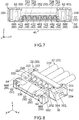
Fig. 9 is a plan view showing the connector ofFig. 8 , wherein an outline of the cover shell is partially illustrated with dashed line. -
Fig. 10 is a perspective view showing a base structure of the connector ofFig. 8 . -
Fig. 11 is another perspective view showing the base structure ofFig. 10 . -
Fig. 12 is a plan view showing a conductor structure of the base structure ofFig. 10 , wherein an outline of a connection portion of the ground member is illustrated with dashed line. -
Fig. 13 is a front view showing the conductor structure ofFig. 12 . -
Fig. 14 is a perspective view showing a base shell and terminals of the conductor structure ofFig. 12 . -
Fig. 15 is another perspective view showing the base shell and the terminals ofFig. 14 . -
Fig. 16 is a bottom view showing the base shell and the terminals ofFig. 14 . -
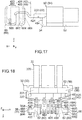
Fig. 17 is a side view showing the base shell and the terminals ofFig. 14 , wherein an outline of a ground portion of the ground member and an outline of the cable are illustrated with dashed line. -
Fig. 18 is a plan view showing the connector ofFig. 9 , wherein a holding member of the connector is not illustrated, and outlines of hidden parts of the cables and outlines of hidden parts of the terminals are illustrated with dashed line. -
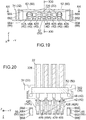
Fig. 19 is a front view showing the connector ofFig. 18 . -
Fig. 20 is a cross-sectional view showing the connector ofFig. 19 , taken along line XX-XX. -
Fig. 21 is a cross-sectional view showing the connector ofFig. 19 , taken along line XXI-XXI. -
Fig. 22 is a perspective view showing a cable connector and an on-board connector ofPatent Document 1. -
Fig. 23 is an exploded, perspective view showing the cable connector ofFig. 22 . - While the invention is susceptible to various modifications and alternative forms, specific embodiments thereof are shown by way of example in the drawings and will herein be described in detail. It should be understood, however, that the drawings and detailed description thereto are not intended to limit the invention to the particular form disclosed, but on the contrary, the intention is to cover all modifications, equivalents and alternatives falling within the spirit and scope of the present invention as defined by the appended claims.
- As shown in
Figs. 1 and 2 , aconnector assembly 10 according to an embodiment of the present invention comprises aconnector 30 and amating connector 70. Theconnector 30 is a cable connector configured to be connected to a plurality ofcables 22. Theconnector 30 forms aharness 20 together with thecables 22. Thus, theharness 20 comprises theconnector 30 and a plurality of thecables 22. Themating connector 70 is an on-board connector configured to be mounted on aboard 80. - Each of the
cables 22 of the present embodiment is a coaxial cable. Each of thecables 22 is connected to an antenna (not shown) and transmits signals of the antenna. Theboard 80 of the present embodiment is installed in an electronic device (not shown) which sends and receives signals via the antennas. Theconnector assembly 10 of the present embodiment transmits the signals between the antennas and the electronic device. However, the usage of thecables 22 and theconnector assembly 10 of the present invention is not limited specifically. - Referring to
Fig. 1 , each of thecables 22 of the present embodiment has acore wire 222 made of conductor, aninner insulator 224 made of insulator, anouter conductor 226 made of conductor and anouter insulator 228 made of insulator. Each of thecore wires 222 transmits signals. Each of theinner insulators 224 covers and insulates thecore wire 222. Each of thecore wires 222 is partially exposed from theinner insulator 224 and is connected to theconnector 30. Each of theouter conductors 226 covers theinner insulator 224 and electro-magnetically shields thecore wire 222. Each of theouter insulators 228 covers and insulates theouter conductor 226. Each of theouter conductors 226 is partially exposed from theouter insulator 228 and is connected to theconnector 30. - Each of the
cables 22 of the present embodiment has the aforementioned structure. However, the structure of each of thecables 22 is not limited to the present embodiment, provided that each of thecables 22 has thecore wire 222 for transmitting signals and theouter conductor 226 having ground potential. - Hereafter, explanation will be made about a structure for mating the
connector 30 with themating connector 70 according to the present embodiment. - Referring to
Figs. 1 and 2 , theconnector 30 of the present embodiment comprises afit portion 30M and a receivingportion 30R. Thefit portion 30M is located in the vicinity of a front end (positive X-side end) of theconnector 30 in a front-rear direction (X-direction) perpendicular to the Z-direction and extends along a pitch direction (Y-direction) perpendicular to both the X-direction and the Z-direction. The receivingportion 30R is located rearward of thefit portion 30M and faces the negative X-side of thefit portion 30M. The receivingportion 30R extends along the Y-direction and opens outward at opposite sides in the Y-direction. The receivingportion 30R is a space which is recessed upward, i.e. in the positive Z-direction, so that thefit portion 30M projects downward, i.e. in the negative Z-direction. - The
mating connector 70 of the present embodiment comprises amating receiving portion 70R which is mateable with thefit portion 30M. Themating receiving portion 70R is a space which is recessed downward and opens upward. Themating receiving portion 70R is located at the middle of themating connector 70 in a horizontal plane (XY-plane) perpendicular to the Z-direction. Themating receiving portion 70R extends along the Y-direction. - The
connector 30 is mateable with themating connector 70, which is mounted on theboard 80, from above in an upper-lower direction (Z-direction). In detail, thefit portion 30M can be inserted into themating receiving portion 70R along the Z-direction. When thefit portion 30M is inserted in themating receiving portion 70R, a rear part (negative X-side part) of themating connector 70 is received in the receivingportion 30R. At that time, theconnector 30 is under a mated state where theconnector 30 is mated with themating connector 70. Each of thecables 22 is electrically connected with theboard 80 under the mated state. Theconnector 30 mated with themating connector 70 can be removed from themating connector 70 by removing thefit portion 30M upward from themating receiving portion 70R. - Referring to
Fig. 3 , because of the aforementioned structure for mating theconnector 30 with themating connector 70 according to the present embodiment, the size of theconnector assembly 10 in the Z-direction under the mated state is substantially equal to the size of theconnector 30 in the Z-direction. Referring toFig. 2 , the size of theconnector assembly 10 in the Y-direction under the mated state is substantially equal to the size of theconnector 30 in the Y-direction. However, the structure for mating theconnector 30 with themating connector 70 is not specifically limited, provided that theconnector 30 and themating connector 70 are mateable with each other along the Z-direction. - Hereafter, explanation will be made about a structure of the
mating connector 70 of the present embodiment. - Referring to
Figs. 1 to 3 , themating connector 70 of the present embodiment comprises a plurality ofmating terminals 72 each made of conductor such as metal, amating holding member 74 made of insulator and twoholddowns 76 each made of conductor such as metal. Referring toFig. 1 , themating receiving portion 70R is formed in themating holding member 74. - Referring to
Figs. 1 and4 , themating terminals 72 are held by themating holding member 74 and are arranged in a single row along themating receiving portion 70R. Themating terminals 72 have shapes same as each other. Each of themating terminals 72 is partially exposed in themating receiving portion 70R and is partially exposed downward. Referring toFig. 3 , when themating connector 70 is mounted on theboard 80, a lower end (negative Z-side end) of each of themating terminals 72 is fixed on and connected to a conductive pad (not shown) of theboard 80 via soldering, etc. - Referring to
Figs. 4 and5 , themating terminals 72 consist of a plurality ofmating signal terminals 722 and a plurality ofmating ground terminals 728. Thus, themating connector 70 comprises a plurality of themating signal terminals 722 and a plurality of themating ground terminals 728. Themating signal terminals 722 and themating ground terminals 728 are arranged alternately in the Y-direction. Referring toFig. 1 , themating signal terminals 722 are provided so as to correspond to thecables 22, respectively. Each of themating signal terminals 722 transmits signals between thecore wire 222 of the correspondingcable 22 and theboard 80 under the mated state (seeFig. 2 ). Each of themating ground terminals 728 grounds theouter conductors 226 of thecables 22 to theboard 80 under the mated state. - Referring to
Figs. 1, 2 ,4 and5 , the twoholddowns 76 are arranged at opposite sides of themating receiving portion 70R in the Y-direction, respectively, and are held by themating holding member 74. The two holddowns 76 have shapes which are mirror images to each other with respect to a perpendicular plane defined by the X-direction and the Z-direction. Each of theholddowns 76 is partially exposed in themating receiving portion 70R and partially extends downward to be exposed downward. Referring toFig. 3 , when themating connector 70 is mounted on theboard 80, a lower end of each of theholddowns 76 is fixed on and connected to a conductive pad (not shown) of theboard 80 via soldering, etc. Each of the holddowns 76 grounds the outer conductors 226 (seeFig. 1 ) of thecables 22 to theboard 80 under the mated state. - Referring to
Figs. 1 and5 , each of theholddowns 76 is provided with twolock projections 762. The twolock projections 762 are located in themating receiving portion 70R and project toward each other in the X-direction. Referring toFig. 5 , when thefit portion 30M is received in themating receiving portion 70R, the twolock projections 762 of each of theholddowns 76 sandwich and hold thefit portion 30M in the X-direction to lock the mated state. - The
mating connector 70 of the present embodiment has the aforementioned structure. However, the present invention is not limited thereto. The structure of themating connector 70 can be variously modified, provided that the structure of themating connector 70 corresponds to the structure of the connector 30 (seeFig. 1 ). For example, themating signal terminal 722 and themating ground terminal 728 may have shapes different from each other. The two holddowns 76 may have shapes which are not mirror images to each other. Thelock projections 762 may be provided as necessary. Themating connector 70 may further comprise another member in addition to the aforementioned members. - Hereafter, explanation will be made about a structure of the
connector 30 of the present embodiment. - Referring to
Figs. 6 and8 , theconnector 30 of the present embodiment comprises abase structure 32, a cable-holdingstructure 36 and acover shell 38 made of conductor. Theconnector 30 of the present embodiment is formed of only the aforementioned structures and member. However, the present invention is not limited thereto. For example, theconnector 30 may further comprise another structure or member in addition to the aforementioned structures and member. - Referring to
Fig. 10 , thebase structure 32 of the present embodiment comprises a holdingmember 33 made of insulator and aconductor structure 34. The holdingmember 33 is a unitary molded member. Theconductor structure 34 is an assembly formed of a plurality of members each made of conductor. Theconductor structure 34 is insert-molded in the holdingmember 33 to be held by the holdingmember 33. Thus, theconnector 30 of the present embodiment comprises the single holdingmember 33 in which theconductor structure 34 is embedded. However, the present invention is not limited thereto. For example, the holdingmember 33 may be formed of a plurality of members combined to each other. Theconductor structure 34 may be partially press-fit in the holdingmember 33 to be held by the holdingmember 33. - Referring to
Figs. 10 and11 , the holdingmember 33 of the present embodiment has twoaccommodation walls 332 and a holdingportion 336. As shown inFig. 10 , theaccommodation walls 332 are rear parts of the holdingmember 33 and are located at opposite sides of the holdingmember 33 in the Y-direction, respectively. Each of theaccommodation walls 332 is formed with a recessedportion 333 and anengagement projection 334. Each of the recessedportions 333 is a recess which is located on an inner side of theaccommodation wall 332 and is recessed outward of the holdingmember 33 in the Y-direction. The two recessedportions 333 face each other in the Y-direction. Each of theengagement projections 334 is provided on an outer wall surface of theaccommodation wall 332 in the Y-direction and projects outward in the Y-direction. The holdingportion 336 is a front part (positive X-side part) of the holdingmember 33 and extends along the Y-direction over the holdingmember 33. The holdingportion 336 works as thefit portion 30M (seeFig. 1 ) of theconnector 30. - The holding
member 33 of the present embodiment has the aforementioned structure. However, the structure of the holdingmember 33 is not specifically limited, provided that theconductor structure 34 can be held by the holdingmember 33. - Referring to
Figs. 10 and11 , theconductor structure 34 of the present embodiment includes a plurality ofterminals 40 each made of conductor, abase shell 50 made of conductor and twoground members 60 each made of conductor. Thus, theconnector 30 of the present embodiment comprises a plurality of theterminals 40, thebase shell 50 and the twoground members 60. Theconductor structure 34 of the present embodiment is formed of only theterminals 40, thebase shell 50 and theground members 60. However, the present invention is not limited thereto. For example, thebase shell 50 may be provided as necessary. Instead, theconductor structure 34 may further comprise another member in addition to the aforementioned members. - Referring to
Figs. 14 and15 , thebase shell 50 of the present embodiment is a part of a single metal plate with bends. Thebase shell 50 has a flat-plate portion 52 and acoupling portion 54. The flat-plate portion 52 extends in parallel to the horizontal plane (XY-plane) perpendicular to the Z-direction. Thecoupling portion 54 is connected to a front end of the flat-plate portion 52 and extends upward and forward (i.e. in the positive X-direction) in an arc. The flat-plate portion 52 is formed with twojoint holes 522. Each of thejoint holes 522 is a hole which passes through the flat-plate portion 52 in the Z-direction. - Referring to
Figs. 10 and11 , thebase shell 50 is embedded in the holdingmember 33 except for a joint portion which is a part of the flat-plate portion 52 formed with the joint holes 522. The joint portion of the flat-plate portion 52 is entirely exposed from the holdingmember 33 and is arranged so as to couple lower ends of the twoaccommodation walls 332 of the holdingmember 33 to each other. - Referring to
Fig. 11 , theterminals 40 of the present embodiment are arranged in a single row in the Y-direction to form aterminal row 40R. Each of theterminals 40 is embedded in the holdingmember 33. Referring toFig. 11 together withFig. 1 , theterminals 40 are provided so as to correspond to themating terminals 72 of themating connector 70, respectively. Each of theterminals 40 is exposed from the holdingportion 336 which is thefit portion 30M. Referring toFig 7 , each of the thus-arrangedterminals 40 is brought into contact with thecorresponding mating terminal 72 under the mated state to be electrically connected with thecorresponding mating terminal 72. - Referring to
Figs. 14 and15 , theterminals 40 include a plurality ofsignal terminals 42 and a plurality ofground terminals 48. Each of thesignal terminals 42 is a member separated from thebase shell 50. More specifically, each of thesignal terminals 42 is a single metal plate of constant thickness with bends. In contrast, each of theground terminals 48 is a member integral with thebase shell 50. More specifically, each of theground terminals 48 is a single metal piece of constant thickness with bends and is coupled to thebase shell 50. In detail, each of theground terminals 48 has acoupling portion 484. Each of thecoupling portions 484 is connected to a front end of thecoupling portion 54 of thebase shell 50 and extends forward therefrom. However, the present invention is not limited thereto. For example, each of theground terminals 48 may be a member separable from thebase shell 50 and may be in contact with thebase shell 50. - Referring to
Fig. 11 , thesignal terminals 42 and theground terminals 48 are held by the holdingmember 33. Thesignal terminals 42 and theground terminals 48 of the present embodiment are insert-molded in the holdingmember 33 and are embedded in the holdingmember 33. However, the present invention is not limited thereto. For example, thesignal terminals 42 and theground terminals 48 may be press-fit in the holdingmember 33 to be held by the holdingmember 33. - Referring to
Figs. 10 and11 , theground members 60 are attached to the holdingmember 33. Theground members 60 of the present embodiment are insert-molded in the holdingmember 33. However, the present invention is not limited thereto. For example, theground members 60 may be fit in the holdingmember 33. - The
ground members 60 of the present embodiment are embedded in opposite sides of the holdingportion 336 of the holdingmember 33 in the Y-direction, respectively. Each of theground members 60 has a connectingportion 62, acoupling portion 64 and aground portion 66. Each of the connectingportions 62 is exposed from an upper surface (positive Z-side surface) of the holdingportion 336. Each of thecoupling portions 64 couples the connectingportion 62 and theground portion 66 to each other. Each of theground portions 66 is exposed from side surfaces and a lower surface (negative Z-side surface) of the holdingportion 336. - Referring to
Figs. 10 and11 together withFig. 1 , theground members 60 are provided so as to correspond to theholddowns 76 of the mating connector 70 (seeFig. 1 ), respectively. Referring toFig. 5 , each of theground portions 66 is connected to the correspondingholddown 76 under the mated state. In detail, each of theground portions 66 is brought into contact with the correspondingholddown 76 to be electrically connected to the correspondingholddown 76 under the mated state. - Each of the
ground portions 66 of the present embodiment is pressed against thelock projection 762 of the correspondingholddown 76 under the mated state so that the mated state is frictionally locked. Thus, theground portions 66 of theground members 60 lock the mated state together with theholddowns 76 of themating connector 70. However, the present invention is not limited thereto. For example, theground portions 66 may be engaged with theholddowns 76, respectively, to lock the mated state. Moreover, the mated state may be locked by a part other than theground portions 66. In this instance, each of theground portions 66 may be merely in contact with theholddown 76. - Each of the
terminals 40 and theground members 60 of the present embodiment roughly has the aforementioned structure. The structure of each of theterminals 40 and theground portions 66 of theground members 60 will be described later in detail. - Referring to
Fig 8 , the cable-holdingstructure 36 of the present embodiment holds a plurality of thecables 22 together. The cable-holdingstructure 36 comprises twoground bars 362 each made of conductor and aconductive member 364. Each of the ground bars 362 has a rectangular flat-plate shape. The twoground bars 362 vertically sandwich theouter conductors 226 which are exposed from theouter insulators 228. Theconductive member 364 of the present embodiment is solder which fills space between the two ground bars 362. According to the aforementioned structure, each of the ground bars 362 is connected to theouter conductors 226 of thecables 22 to have ground potential same as that of theouter conductors 226. - Referring to
Figs 8 and9 , the cable-holdingstructure 36 which holds thecables 22 is accommodated in a space formed between the twoaccommodation walls 332 of the holdingmember 33. The opposite ends of the cable-holdingstructure 36 in the Y-direction are received in the recessedportions 333 of theaccommodation walls 332, respectively. - Referring to
Fig. 11 together withFig. 8 , the cable-holdingstructure 36 which is accommodated as described above is fixed to the flat-plate portion 52 of thebase shell 50. According to the present embodiment, thejoint holes 522 of thebase shell 50 are filled with solder (not shown) so that thebase shell 50 is fixed and connected to the lower (negative Z-side)ground bar 362 of the cable-holdingstructure 36. Thus, thebase shell 50 is electrically connected with theouter conductors 226 of thecables 22 to have ground potential same as that of theouter conductors 226. Thebase shell 50 of the present embodiment is indirectly connected to theouter conductors 226 via the cable-holdingstructure 36. However, the present invention is not limited thereto. For example, thebase shell 50 may be directly connected to theouter conductors 226. - Referring to
Figs. 2 ,3 ,6 and7 , thecover shell 38 of the present embodiment is a single metal plate with bends and has a flat-plate portion 382 and twoside plate portions 386. The flat-plate portion 382 extends in parallel to the XY-plane. Theside plate portions 386 are connected to opposite sides of the flat-plate portion 382 in the Y-direction, respectively. Each of theside plate portions 386 extends in parallel to the XZ-plane. - Referring to
Fig. 2 , the flat-plate portion 382 is formed with two frontjoint holes 383 and two rear joint holes 384. Each of the frontjoint holes 383 and the rearjoint holes 384 is a hole which passes through the flat-plate portion 382 in the Z-direction. The frontjoint holes 383 are located at a front part of the flat-plate portion 382. The rearjoint holes 384 are located at a rear part of the flat-plate portion 382. Referring toFigs. 2 ,3 and6 , each of theside plate portions 386 is formed with anengagement hole 388. Each of the engagement holes 388 is a hole which passes through theside plate portion 386 in the Y-direction. - The
cover shell 38 is attached to thebase structure 32 from above. Theengagement projections 334 of thebase structure 32 are engaged with the engagement holes 388 of thecover shell 38, respectively, and the flat-plate portion 382 of thecover shell 38 almost entirely covers thebase structure 32 from above. - Referring to
Fig 9 , thecover shell 38 which is attached as described above is fixed to the cable-holdingstructure 36. According to the present embodiment, the rearjoint holes 384 of thecover shell 38 are filled with solder (not shown) so that thecover shell 38 is fixed and connected to the upper (positive Z-side)ground bar 362 of the cable-holdingstructure 36. Thus, thecover shell 38 is electrically connected with the outer conductors 226 (seeFig. 8 ) of thecables 22 to have ground potential same as that of theouter conductors 226. Thecover shell 38 of the present embodiment is indirectly connected to theouter conductors 226 via the cable-holdingstructure 36. However, the present invention is not limited thereto. For example, thecover shell 38 may be directly connected to theouter conductors 226. - Referring to
Fig. 6 , an upper part of the holdingmember 33 and opposite sides of the holdingmember 33 in the Y-direction are, at least in part, covered by thecover shell 38. In addition, a lower part of the holdingmember 33 is, at least in part, covered by thebase shell 50. In other words, the holdingmember 33 of the present embodiment is, at least in part, covered by thecover shell 38 and thebase shell 50, i.e. the two shells which are formed separately from each other, in the YZ-plane. However, the present invention is not limited thereto. For example, thecover shell 38 and thebase shell 50 may be an integral member. Moreover, the structure of each of thecover shell 38 and thebase shell 50 is not limited to the present embodiment. - Referring to
Fig 9 , the flat-plate portion 382 of thecover shell 38 is fixed to the twoground members 60 in addition to the cable-holdingstructure 36. According to the present embodiment, each of the frontjoint holes 383 of thecover shell 38 are filled with solder (not shown) so that thecover shell 38 is fixed and connected to the connectingportions 62 of the twoground members 60. As a result, each of theground members 60 is electrically connected with the outer conductors 226 (seeFig. 8 ) of thecables 22 to have ground potential same as that of theouter conductors 226. Thus, theconnector 30 comprises theground members 60 which are configured to be connected to theouter conductors 226 of thecables 22. - Each of the
ground members 60 of the present embodiment is indirectly connected to the outer conductors 226 (seeFig. 8 ) via thecover shell 38 which is formed separately from theground members 60. However, the present invention is not limited thereto. For example, each of theground members 60 may be a member integral with thecover shell 38. Each of theground members 60 may be indirectly connected to theouter conductors 226 via thebase shell 50 or may be directly connected to theouter conductors 226. - Hereafter, further specific explanation will be made about the structure of each of the
terminals 40 and theground portions 66 of theground members 60. - Referring to
Fig. 18 , thesignal terminals 42 are provided so as to correspond to thecables 22, respectively. Theground terminals 48 are connected to theouter conductors 226 of thecables 22 via thebase shell 50. Thus, theterminals 40 include a plurality of thesignal terminals 42 which correspond to thecables 22, respectively, and a plurality of theground terminals 48 which are configured to be connected with theouter conductors 226 of thecables 22. - For the
connector 30 of the present embodiment, only theterminals 40 are configured to be connected to the mating terminals 72 (seeFig. 1 ) of the mating connector 70 (seeFig. 1 ). Theterminals 40 consist of thesignal terminals 42 and theground terminals 48. However, the present invention is not limited thereto. For example, theterminals 40 of theconnector 30 may be terminals which transmit low-speed signals together with themating terminals 72. Themating connector 70 may comprise additional mating terminals (not shown) for transmitting high-speed signals in addition to themating terminals 72. In this instance, theconnector 30 may comprise additional terminals configured to be connected to the additional mating terminals in addition to theterminals 40. - Referring to
Fig. 14 , thesignal terminals 42 have basic structures same as each other. More specifically, each of thesignal terminals 42 has afirst contact portion 422, aconnection portion 424 and afirst adjustment portion 426. Each of thefirst contact portions 422 extends rearward from a front end of thesignal terminal 42 in the X-direction and has a J-like shape in the XZ-plane. Each of theconnection portions 424 linearly extends forward from a rear end (negative X-side end) of thesignal terminal 42. Each of thefirst adjustment portions 426 extends from thefirst contact portion 422 to theconnection portion 424 in the X-direction. In detail, each of thefirst adjustment portions 426 linearly extends rearward from a rear end of thefirst contact portion 422 and then slopes downward to a front end of theconnection portion 424. - Each of the
signal terminals 42 of the present embodiment has the aforementioned basic structure. However, the present invention is not limited thereto. For example, each of thesignal terminals 42 may further have another part in addition to the aforementioned portions. - Referring to
Fig. 11 , each of thefirst contact portions 422 is exposed from a front surface (positive X-side surface), a rear surface (negative X-side surface) and a lower surface of the holdingportion 336. Referring toFig 7 , thefirst contact portions 422 correspond to themating signal terminals 722, respectively. Thefirst contact portions 422 are brought into contact with themating signal terminals 722 under the mated state, respectively. Referring toFig 9 , thecore wires 222 exposed from theinner insulators 224 are fixed on and connected to theconnection portions 424, respectively, via soldering, etc. Thus, each of thesignal terminals 42 has theconnection portion 424 which is configured to be connected to thecore wire 222 of the correspondingcable 22. Referring toFig. 7 together withFig. 1 , themating signal terminals 722 are electrically connected with thecore wires 222 of thecables 22 via thesignal terminals 42 under the mated state, respectively. - Referring to
Fig. 14 , theground terminals 48 have basic structures same as each other. More specifically, each of theground terminals 48 has asecond contact portion 482 and asecond adjustment portion 486 in addition to the previously describedcoupling portion 484. Each of thesecond contact portions 482 extends rearward from a front end of theground terminal 48 in the X-direction and has a J-like shape in the XZ-plane. Each of thesecond adjustment portions 486 extends from thesecond contact portion 482 to thecoupling portion 484 in the X-direction. In detail, each ofsecond adjustment portion 486 linearly extends from a rear end of thesecond contact portion 482 and then slopes downward to a front end of thecoupling portion 484. - Each of the
ground terminals 48 of the present embodiment has the aforementioned basic structure. However, the present invention is not limited thereto. For example, as previously described, each of theground terminals 48 may be a member formed separately from thebase shell 50. In this instance, each of theground terminals 48 may be connected to thebase shell 50 via a member formed separately from theground terminal 48. According to this modification, each ofsecond adjustment portion 486 does not need to be provided with thecoupling portion 484 but may extend from thesecond contact portion 482 to the rear end of theground terminal 48 in the X-direction. Instead, each of theground terminals 48 may further have another part in addition to the aforementioned portions. - Referring to
Fig. 11 , each of thesecond contact portions 482 is exposed from the front surface, the rear surface and the lower surface of the holdingportion 336. Referring toFig 7 , thesecond contact portions 482 correspond to themating ground terminals 728, respectively. Thesecond contact portions 482 are brought into contact with themating ground terminals 728 under the mated state, respectively. Referring toFig. 7 together withFig. 1 , themating ground terminals 728 are electrically connected with theouter conductors 226 of thecables 22 via theground terminals 48 under the mated state. - Referring to
Fig. 14 , thefirst contact portion 422 and theconnection portion 424 of each of thesignal terminals 42 are apart from each other in the X-direction. According to this structure, each of thesignal terminals 42 can be reduced in size in the Z-direction while a size of thesignal terminal 42 in the X-direction is made large. Thus, this structure enables the connector 30 (seeFig. 6 ) to be reduced in size in the Z-direction. - Referring to
Figs. 14 and15 , thesignal terminals 42 and theground terminals 48 are alternately arranged in the Y-direction to form oneterminal row 40R. Referring toFig. 15 , thesignal terminals 42 of the present embodiment include twoouter signal terminals 42A and twoinner signal terminals 42B. Each of theouter signal terminals 42A is located at an end of theterminal row 40R in the Y-direction. Each of theinner signal terminals 42B is located between adjacent two of theground terminals 48 in theterminal row 40R in the Y-direction. In other words, each of theinner signal terminals 42B is located at an inner position of theterminal row 40R in the Y-direction. Theground terminals 48 of the present embodiment include twoouter ground terminals 48A and oneinner ground terminal 48B. Each of theouter ground terminals 48A is located between one of theouter signal terminals 42A and one of theinner signal terminals 42B in the Y-direction. Theinner ground terminal 48B is located between the twoinner signal terminals 42B in the Y-direction. - A typical arrangement of a terminal row of an existing cable connector is different from the aforementioned arrangement of the present embodiment. Specifically, every signal terminal is arranged between two of ground terminals. Thus, not two of the signal terminals but two of the ground terminals are arranged at opposite ends of the terminal row, respectively. Referring to
Fig. 11 together withFig. 6 , according to the present embodiment, theground terminals 48 are removed from the opposite ends of theterminal row 40R arranged in the Y-direction. Therefore, theconnector 30 has a size in the Y-direction smaller than that of the existing connector which has theground terminals 48 arranged at the opposite ends of theterminal row 40R. Thus, the present embodiment enables theconnector 30 to be reduced in size in the Y-direction. - Referring to
Fig. 12 , thefirst contact portions 422 of all thesignal terminals 42 and thesecond contact portions 482 of all theground terminals 48 are arranged at regular intervals CI in the Y-direction. In other words, thefirst contact portions 422 and thesecond contact portions 482 of all theterminals 40 are arranged at equal pitches. This arrangement enables theconnector 30 to be further reduced in size in the Y-direction by minimizing the regular interval CI in accordance with the structure of the connector 30 (seeFig. 6 ). - Referring to
Fig. 15 , the number of theouter signal terminals 42A of the present embodiment is two. The twoouter signal terminals 42A are located at the opposite ends of theterminal row 40R in the Y-direction, respectively. Theterminals 40 of the present embodiment consist of N of thesignal terminals 42 and (N-1) of theground terminals 48, N being an odd number of three or more. However, the present invention is not limited thereto. For example, the number of theouter signal terminals 42A may be one. In this instance, one of theouter signal terminals 42A and one of theouter ground terminals 48A may be located at the opposite ends of theterminal row 40R in the Y-direction, respectively. However, the arrangement of the present embodiment is preferable in order to reduce the size of the connector 30 (seeFig. 6 ) in the Y-direction as possible. - If one of the ground terminals, which is located at an end of the typical terminal row of the existing cable connector, is removed therefrom similarly to the present embodiment, one of the signal terminals is located at the end of the terminal row instead of the removed ground terminal. The outer signal terminal, i.e. the signal terminal located at the end of the terminal row, tends to have impedance higher than that of the inner signal terminal located at an inner position of the terminal row, i.e. the signal terminal located between two of the ground terminals. When the impedance of the outer signal terminal is higher than that of the inner signal terminal, the transmission characteristics of the connector might be degraded as a whole. As can be seen from this fact, the
terminal row 40R of the present embodiment cannot be easily conceived from the typical terminal row of the existing cable connector. - Referring to
Fig. 12 , the connector 30 (seeFig. 6 ) of the present embodiment has an impedance adjustment mechanism which makes the impedance of theouter signal terminal 42A and the impedance of theinner signal terminal 42B be close to each other. This impedance adjustment mechanism includes theground portions 66 of theground members 60 in addition to thesignal terminals 42 and theground terminals 48. Hereafter, explanation will be made about the impedance adjustment mechanism of the present embodiment. - Referring to
Figs. 13 ,18 and19 , theground portion 66 of each of theground members 60 of the present embodiment has aside plate 662, alower plate 664, afront plate 666 and arear plate 668. - Referring to
Fig. 10 , each of theside plates 662 extends downward from an outer end of thecoupling portion 64 in the Y-direction and extends in parallel to the XZ-plane. Referring toFig. 11 , each of theside plates 662 is embedded in a side surface of an outer portion, which is an outer part of the holdingportion 336 in the Y-direction, and is exposed outward in the Y-direction. Each of thelower plates 664 is connected to a lower end of theside plate 662 and extends in parallel to the XY-plane. Each of thelower plates 664 is embedded in a lower surface of the outer portion of the holdingportion 336 and is exposed downward. Each of thefront plates 666 extends upward from a front end of thelower plate 664 in parallel to the YZ-plane. Each of thefront plates 666 is embedded in a front surface of the outer portion of the holdingportion 336 and is exposed forward. Each of therear plates 668 extends upward from a rear end of thelower plate 664 in parallel to the YZ-plane. Each of therear plates 668 is embedded in a rear surface of the outer portion of the holdingportion 336 and is exposed rearward. - Each of the
ground portions 66 of the present embodiment has the aforementioned structure. However, the structure of each of theground portions 66 is not specifically limited, provide that theground portions 66 contribute to the impedance adjustment of thesignal terminals 42 as described later. - Referring to
Figs. 19 and 20 , each of theouter signal terminals 42A is located between theground portion 66 of theground member 60 and theouter ground terminal 48A, which is one of theground terminals 48, in the Y-direction. Thus, one of theground portions 66, each of which is a part of theground member 60, is arranged outward of each of theouter signal terminals 42A in the Y-direction. As previously described, theground members 60 are connected with theouter conductors 226 of thecables 22, and thereby each of theground portions 66 has ground potential. - Referring to
Fig. 12 , each of theground portions 66 is apart from thefirst contact portion 422 of theouter signal terminal 42A in the Y-direction by a distance DG longer than the regular interval CI. Meanwhile, thefirst adjustment portion 426 of each of theouter signal terminals 42A protrudes toward theground portion 66 in the Y-direction. Referring toFigs. 17 and21 , the position of thefirst adjustment portion 426 of each of theouter signal terminals 42A in the XZ-plane is equal to or overlaps with the position of theground portion 66 in the XZ-plane. These structures enable the impedance of each of theouter signal terminals 42A to be lowered even when the distance DG is longer than the regular interval CI. - Referring to
Fig. 12 , according to the present embodiment, the impedance of each of theouter signal terminals 42A can be lowered to be close to the impedance of theinner signal terminal 42B which is thesignal terminal 42 located between two of theground terminals 48, so that degradation of transmission characteristics of the connector 30 (seeFig. 1 ) can be prevented as a whole. Thus, the present embodiment provides theconnector 30 which can be reduced in size in the Y-direction as well as size in the Z-direction, while degradation of transmission characteristics is prevented. - According to the present embodiment, the
first adjustment portion 426 of each of theouter signal terminals 42A entirely protrudes toward theground portion 66 in the Y-direction. In detail, each of theouter signal terminals 42A of the present embodiment has twofirst protrusions 429 consisting of a firstouter protrusion 429A and a firstinner protrusion 429B. The twofirst protrusions 429 are formed on opposite sides of theouter signal terminal 42A in the Y-direction, respectively, and protrude beyond thefirst contact portion 422 in orientations opposite to each other in the Y-direction. Each of thefirst protrusions 429 extends rearward from the rear end of thefirst contact portion 422 over the wholefirst adjustment portion 426. In particular, the firstouter protrusion 429A protrudes beyond thefirst contact portion 422 toward theground portion 66 in the Y-direction. - Each of the
outer signal terminals 42A of the present embodiment has the aforementioned protrusions. However, the present invention is not limited thereto. For example, each of the firstouter protrusions 429A may be partially provided on thefirst adjustment portion 426 of theouter signal terminal 42A. Thus, thefirst adjustment portion 426 of each of theouter signal terminals 42A may at least partially protrude toward theground portion 66 in the Y-direction. - Referring to
Figs. 17 and21 , according to the present embodiment, the position of thefirst adjustment portion 426 of each of theouter signal terminals 42A in the XZ-plane overlaps with the position of theground portion 66 in the XZ-plane. In detail, when theouter signal terminal 42A and theground portion 66 are seen along the Y-direction, thefirst adjustment portion 426 overlaps with therear plate 668 and theside plate 662 of theground portion 66. However, the present invention is not limited thereto. For example, when theouter signal terminal 42A and theground portion 66 are seen along the Y-direction, thefirst adjustment portion 426 may be entirely located in theground portion 66. Thus, the position of thefirst adjustment portion 426 of each of theouter signal terminals 42A in the XZ-plane may be equal to or overlap with the position of theground portion 66 in the XZ-plane. Moreover, each of theground portions 66 may have an additional plate in addition to theside plate 662 or instead of theside plate 662. The additional plate may be located at an inner side of theground portion 66 in the Y-direction. - Referring to
Fig. 16 , thefirst adjustment portion 426 of each of theinner signal terminals 42B of the present embodiment is apart from thesecond adjustment portion 486 of each of adjacent two of theground terminals 48 by an inner predetermined distance DI in the Y-direction. Thefirst adjustment portion 426 of each of theouter signal terminals 42A is apart from thesecond adjustment portion 486 of theouter ground terminal 48A, i.e. adjacent one of theground terminals 48, by an outer predetermined distance DE in the Y-direction. The inner predetermined distance DI is longer than the outer predetermined distance DE. - According to the present embodiment, because the
first adjustment portion 426 of each of theinner signal terminals 42B is located to be far away from each of theground terminals 48, the impedance of theinner signal terminal 42B can be made high. Thus, the impedance of each of theinner signal terminals 42B is made higher to be close to the impedance of each of theouter signal terminals 42A. As a result, degradation of transmission characteristics of the connector 30 (seeFig. 1 ) can be prevented as a whole. However, the present invention is not limited thereto. For example, when the impedance of each of theouter signal terminals 42A can be sufficiently lowered, the impedance of each of theinner signal terminals 42B does not need to be made high. - The
first adjustment portion 426 of each of theinner signal terminals 42B of the present embodiment is recessed inward in the Y-direction so as to be away from thesecond adjustment portion 486 of each of the adjacent two of theground terminals 48 in the Y-direction. In addition, thesecond adjustment portion 486 of each of the adjacent two of theground terminals 48 is recessed inward in the Y-direction so as to be away from thefirst adjustment portion 426 of theinner signal terminal 42B in the Y-direction. More specifically, thesecond adjustment portion 486 of each of theouter ground terminals 48A is recessed inward in the Y-direction so as to be away from thefirst adjustment portion 426 of adjacent one of theinner signal terminals 42B in the Y-direction. Thesecond adjustment portion 486 of theinner ground terminal 48B is recessed inward in the Y-direction so as to be away from thefirst adjustment portion 426 of each of adjacent two of theinner signal terminals 42B in the Y-direction. - In detail, each of the
inner signal terminals 42B of the present embodiment has twofirst recesses 428. The twofirst recesses 428 are formed on opposite sides of theinner signal terminal 42B in the Y-direction, respectively, and are recessed from thefirst contact portion 422 in orientations opposite to each other in the Y-direction. Each of thefirst recesses 428 extends rearward from the rear end of thefirst contact portion 422 over the wholefirst adjustment portion 426. - Each of the
ground terminals 48 has one or twosecond recesses 488. For each of theouter ground terminals 48A, only one of thesecond recesses 488 is formed on an inner side of theouter ground terminal 48A in the Y-direction and is recessed outward of theterminal row 40R (seeFig. 15 ) in the Y-direction from thesecond contact portion 482. For each of theinner ground terminals 48B, two of thesecond recesses 488 are formed on opposite sides of theinner ground terminal 48B in the Y-direction and are recessed from thesecond contact portion 482 in orientations opposite to each other in the Y-direction. Each of thesecond recesses 488 extends rearward from the rear end of thesecond contact portion 482 over the wholesecond adjustment portion 486. - Each of the
inner signal terminals 42B and theground terminals 48 of the present embodiment has the aforementioned recesses. These recesses of the present embodiment enable the inner predetermined distance DI to be longer than the outer predetermined distance DE. However, the present invention is not limited thereto. For example, only thefirst recesses 428 or only thesecond recesses 488 may be provided. - Referring to
Fig. 12 , thefirst adjustment portion 426 of each of theouter signal terminals 42A of the present embodiment protrudes toward thesecond adjustment portion 486 of theouter ground terminal 48A, i.e. the adjacent one of theground terminals 48, in the Y-direction. In addition, thesecond adjustment portion 486 of each of theouter ground terminals 48A, each of which is the adjacent one of theground terminals 48, protrudes toward thefirst adjustment portion 426 of theouter signal terminal 42A in the Y-direction. - In detail, the first
inner protrusion 429B of each of theouter signal terminals 42A of the present embodiment protrudes beyond thefirst contact portion 422 toward theouter ground terminal 48A in the Y-direction. In addition, each of theouter ground terminals 48A has onesecond protrusion 489. For each of theouter ground terminals 48A, thesecond protrusion 489 is formed on an outer side of theouter ground terminal 48A in the Y-direction and protrudes outward in the Y-direction beyond thesecond contact portion 482. Each of thesecond protrusions 489 extends rearward from the rear end of thesecond contact portion 482 over the wholesecond adjustment portion 486. - Referring to
Fig. 16 , each of theouter signal terminals 42A and theouter ground terminals 48A of the present embodiment has the aforementioned protrusion. These protrusions of the present embodiment enable the inner predetermined distance DI to be longer than the outer predetermined distance DE. However, the present invention is not limited thereto. For example, only thefirst protrusions 429 or only thesecond protrusions 489 may be provided. - Referring to
Fig. 12 , according to the present embodiment, a size of the firstouter protrusion 429A in the Y-direction, namely a protruding amount, is larger than a size of the firstinner protrusion 429B in the Y-direction, namely another protruding amount. However, the present invention is not limited thereto. The protruding amount of each of the firstouter protrusions 429A and the firstinner protrusions 429B may be designed in accordance with a positional relation to the other conductors such as the regular interval CI and the distance DG. - Referring to
Fig. 12 , each of theinner signal terminals 42B and theinner ground terminal 48B of the present embodiment has a symmetric shape with respect to the XZ-plane. Each of theouter signal terminals 42A and theouter ground terminals 48A has an asymmetric shape with respect to the XZ-plane. Theterminal row 40R of the present embodiment has a symmetric structure with respect to an imaginary line IL which extends along the X-direction through a middle point of theterminal row 40R in the Y-direction. In other words, theterminal row 40R has a plane symmetric structure with respect to a plane which is in parallel to the XZ-plane and includes the imaginary line IL. In particular, when theterminal row 40R is seen along the Z-direction, theterminal row 40R has a line symmetric structure with respect to the imaginary line IL. According to this symmetric structure, the impedance of thesignal terminals 42 can be easily adjusted. However, the present invention is not limited thereto. For example, theterminal row 40R may have an asymmetric structure with respect to the imaginary line IL. - Referring to
Figs. 14 and17 , thefirst contact portion 422 and thefirst adjustment portion 426 of each of thesignal terminals 42 form a shape, namely a first shape, in the XZ-plane. The first shapes of thesignal terminals 42 are same as each other. Thesecond contact portion 482 and thesecond adjustment portion 486 of each of theground terminals 48 form a shape, namely a second shape, in the XZ-plane. The second shapes of theground terminals 48 are same as each other. The first shape and the second shape are identical to each other. According to this structure, the impedance of thesignal terminals 42 can be adjusted while the size of the connector 30 (seeFig. 6 ) in the XZ-plane is not made large. However, the present invention is not limited thereto. For example, the first shape and the second shape may be different from each other. - Referring to
Fig. 17 , according to the present embodiment, the positions of thefirst adjustment portions 426 of all thesignal terminals 42 in the XZ-plane are completely equal to the positions of thesecond adjustment portions 486 of all theground terminals 48 in the XZ-plane. In addition, the positions of thefirst contact portions 422 of all thesignal terminals 42 in the XZ-plane are completely equal to the positions of thesecond contact portions 482 of all theground terminals 48 in the XZ-plane. According to this arrangement, the impedance of thesignal terminals 42 can be easily adjusted by adjusting the sizes of thefirst adjustment portions 426 and thesecond adjustment portions 486 in the Y-direction. However, the present invention is not limited thereto. For example, a position of each of thefirst adjustment portions 426 in the XZ-plane may be equal to or overlaps with a position of each of thesecond adjustment portions 486 in the XZ-plane. - The present embodiment can be further variously modified in addition to the already described modifications. For example, referring to
Fig. 12 , thefirst contact portions 422, thesecond contact portions 482, theconnection portions 424 and thecoupling portions 484 of the present embodiment have sizes same as each other in the Y-direction and extend straight along the X-direction. However, the present invention is not limited thereto. For example, each of thefirst contact portions 422, thesecond contact portions 482, theconnection portions 424 and thecoupling portions 484 may be bent in the Y-direction. - While there has been described what is believed to be the preferred embodiment of the invention, those skilled in the art will recognize that other and further modifications may be made thereto without departing from the spirit of the invention, and it is intended to claim all such embodiments that fall within the true scope of the invention.
Claims (10)
- A connector configured to be connected to a plurality of cables and mateable with a mating connector from above in an upper-lower direction, the mating connector being mounted on a board, wherein:each of the cables has a core wire and an outer conductor;the mating connector comprises a plurality of mating signal terminals, a plurality of ground terminals and a holddown;the connector comprises a plurality of terminals, a holding member and a ground member which is configured to be connected to the outer conductors of the cables;the terminals include a plurality of signal terminals which correspond to the cables, respectively, and a plurality of ground terminals which are configured to be connected to the outer conductors of the cables;the signal terminals and the ground terminals are held by the holding member and are alternately arranged in a pitch direction perpendicular to the upper-lower direction to form one terminal row;the ground member is attached to the holding member and has a ground portion;the ground portion is connected to the holddown under a mated state where the connector is mated with the mating connector;each of the signal terminals has a first contact portion, a first adjustment portion and a connection portion which is configured to be connected to the core wire of a corresponding one of the cables;the first contact portions are brought into contact with the mating signal terminals, respectively, under the mated state;the first contact portion and the connection portion of each of the signal terminals are apart from each other in a front-rear direction perpendicular to both the upper-lower direction and the pitch direction;each of the first adjustment portions extends from the first contact portion to the connection portion in the front-rear direction;each of the ground terminals has a second contact portion and a second adjustment portion;the second contact portions are brought into contact with the mating ground terminals, respectively, under the mated state;each of the second adjustment portions extends from the second contact portion in the front-rear direction;a position of each of the first adjustment portions in a perpendicular plane defined by the upper-lower direction and the front-rear direction is equal to or overlaps with a position of each of the second adjustment portions in the perpendicular plane;the signal terminals include an outer signal terminal;the outer signal terminal is located at an end of the terminal row and is located between the ground portion of the ground member and one of the ground terminals in the pitch direction;the first adjustment portion of the outer signal terminal at least partially protrudes toward the ground portion in the pitch direction;a position of the first adjustment portion of the outer signal terminal in the perpendicular plane is equal to or overlaps with a position of the ground portion in the perpendicular plane;the first contact portions and the second contact portions are arranged at regular intervals in the pitch direction; andthe ground portion is apart from the first contact portion of the outer signal terminal by a distance longer than the regular interval in the pitch direction.
- The connector as recited in claim 1, wherein:the signal terminals include an inner signal terminal;the inner signal terminal is located between adjacent two of the ground terminals in the terminal row;the first adjustment portion of the inner signal terminal is apart from the second adjustment portion of each of the adjacent two of the ground terminals by an inner predetermined distance in the pitch direction;the first adjustment portion of the outer signal terminal is apart from the second adjustment portion of adjacent one of the ground terminals by an outer predetermined distance in the pitch direction; andthe inner predetermined distance is longer than the outer predetermined distance.
- The connector as recited in claim 2, wherein:the first adjustment portion of the inner signal terminal is recessed inwards in the pitch direction so as to be away from the second adjustment portion of each of the adjacent two of the ground terminals in the pitch direction; andthe second adjustment portion of each of the adjacent two of the ground terminals is recessed inwards in the pitch direction so as to be away from the first adjustment portion of the inner signal terminal in the pitch direction.
- The connector as recited in claim 2 or 3, wherein:the first adjustment portion of the outer signal terminal protrudes toward the second adjustment portion of the adjacent one of the ground terminals in the pitch direction; andthe second adjustment portion of the adjacent one of the ground terminals protrudes toward the first adjustment portion of the outer signal terminal.
- The connector as recited in one of claims 1 to 4, wherein:the first contact portion and the first adjustment portion of each of the signal terminals form a first shape in the perpendicular plane;the second contact portion and the second adjustment portion of each of the ground terminals form a second shape in the perpendicular direction; andthe first shape and the second shape are identical to each other.
- The connector as recited in one of claims 1 to 5, wherein the ground portion of the ground member locks the mated state together with the holddown of the mating connector.
- The connector as recited in one of claims 1 to 6, wherein:the terminals consist of N of the signal terminals and (N-1) of the ground terminals, N being an odd number of three or more; andthe terminal row has a symmetric structure with respect to an imaginary line which extends along the front-rear direction through a middle point of the terminal row in the pitch direction.
- The connector as recited in one of claims 1 to 7, wherein the signal terminals and the ground terminals are insert-molded in the holding member.
- A harness comprising the connector and the plurality of the cables as recited in one of claims 1 to 8.
- A connector assembly comprising the connector and the mating connector as recited in one of claims 1 to 8.
Applications Claiming Priority (1)
| Application Number | Priority Date | Filing Date | Title |
|---|---|---|---|
| JP2020073778A JP7404142B2 (en) | 2020-04-17 | 2020-04-17 | Connectors, harnesses and connector assemblies |
Publications (2)
| Publication Number | Publication Date |
|---|---|
| EP3896795A1 true EP3896795A1 (en) | 2021-10-20 |
| EP3896795B1 EP3896795B1 (en) | 2022-10-05 |
Family
ID=74625821
Family Applications (1)
| Application Number | Title | Priority Date | Filing Date |
|---|---|---|---|
| EP21157006.4A Active EP3896795B1 (en) | 2020-04-17 | 2021-02-13 | Connector, harness and connector assembly |
Country Status (4)
| Country | Link |
|---|---|
| US (1) | US11349260B2 (en) |
| EP (1) | EP3896795B1 (en) |
| JP (1) | JP7404142B2 (en) |
| CN (1) | CN113540897B (en) |
Families Citing this family (8)
| Publication number | Priority date | Publication date | Assignee | Title |
|---|---|---|---|---|
| CN213278574U (en) * | 2020-04-16 | 2021-05-25 | 番禺得意精密电子工业有限公司 | Electric connector and electric connector combination |
| US11641073B2 (en) * | 2020-10-12 | 2023-05-02 | Japan Aviation Electronics Industry, Limited | Connector |
| JP7563342B2 (en) * | 2021-09-06 | 2024-10-08 | I-Pex株式会社 | Electrical Connectors |
| JP7807984B2 (en) * | 2022-05-30 | 2026-01-28 | 日本航空電子工業株式会社 | Connector, mating connector, and connector assembly |
| JP2025106634A (en) * | 2022-05-26 | 2025-07-16 | 宏致電子股▲ふん▼有限公司 | Connector sets and connectors |
| CN115764375B (en) * | 2022-10-20 | 2026-01-06 | 中航光电科技股份有限公司 | A connector |
| JP7837848B2 (en) * | 2022-10-20 | 2026-03-31 | 日本航空電子工業株式会社 | connector |
| CN117373733A (en) * | 2023-10-31 | 2024-01-09 | 广东田津电子技术有限公司 | A signal transmission device and its manufacturing method |
Citations (2)
| Publication number | Priority date | Publication date | Assignee | Title |
|---|---|---|---|---|
| WO2003026078A1 (en) * | 2001-08-01 | 2003-03-27 | Molex Incorporated | Impedance-tuned connector |
| JP2009032517A (en) | 2007-07-26 | 2009-02-12 | Japan Aviation Electronics Industry Ltd | Connector and electronic device having the same |
Family Cites Families (30)
| Publication number | Priority date | Publication date | Assignee | Title |
|---|---|---|---|---|
| JP3564556B2 (en) * | 2001-10-02 | 2004-09-15 | 日本航空電子工業株式会社 | connector |
| JP2006190568A (en) * | 2005-01-06 | 2006-07-20 | Fujitsu Component Ltd | connector |
| JP4222617B2 (en) * | 2005-12-07 | 2009-02-12 | 日本航空電子工業株式会社 | connector |
| JP2007234490A (en) * | 2006-03-03 | 2007-09-13 | Kyocera Elco Corp | Connector for coaxial cable |
| JP2007317554A (en) | 2006-05-26 | 2007-12-06 | Three M Innovative Properties Co | Connector and connector system |
| JP4097681B1 (en) * | 2007-02-01 | 2008-06-11 | 日本航空電子工業株式会社 | connector |
| JP5338261B2 (en) * | 2008-11-04 | 2013-11-13 | 第一精工株式会社 | Electrical connector |
| JP5476713B2 (en) * | 2008-12-22 | 2014-04-23 | 旭硝子株式会社 | Connector, antenna provided with the same, and vehicle window glass provided with the antenna |
| US7892028B2 (en) * | 2009-01-20 | 2011-02-22 | Hon Hai Precision Ind. Co., Ltd. | Cable connector assembly |
| JP4792517B2 (en) * | 2009-07-07 | 2011-10-12 | 日本航空電子工業株式会社 | Connector assembly |
| JP5077363B2 (en) * | 2010-01-21 | 2012-11-21 | 第一精工株式会社 | Connector device |
| JP4922420B2 (en) * | 2010-02-23 | 2012-04-25 | 日本航空電子工業株式会社 | Connector assembly |
| JP5019079B2 (en) * | 2010-03-10 | 2012-09-05 | 第一精工株式会社 | Connector device |
| JP5516040B2 (en) * | 2010-05-07 | 2014-06-11 | 第一精工株式会社 | Electrical connector and electrical connector assembly |
| JP2012059386A (en) | 2010-09-06 | 2012-03-22 | Hirose Electric Co Ltd | High speed transmission electric connector |
| JP5813349B2 (en) * | 2011-03-29 | 2015-11-17 | 日本航空電子工業株式会社 | Connector and connection object |
| JP2013045520A (en) | 2011-08-22 | 2013-03-04 | Panasonic Corp | Header |
| JP5826654B2 (en) * | 2012-02-01 | 2015-12-02 | 日本航空電子工業株式会社 | connector |
| JP2013225475A (en) * | 2012-03-19 | 2013-10-31 | Fujitsu Component Ltd | Contact, connector, and manufacturing method of connector |
| JP6005575B2 (en) * | 2013-04-11 | 2016-10-12 | 日本航空電子工業株式会社 | connector |
| JP6097165B2 (en) * | 2013-07-11 | 2017-03-15 | 日本航空電子工業株式会社 | connector |
| JP6199153B2 (en) * | 2013-10-25 | 2017-09-20 | 日本航空電子工業株式会社 | connector |
| KR102120813B1 (en) * | 2015-01-11 | 2020-06-17 | 몰렉스 엘엘씨 | Circuit board bypass assembly and components therefor |
| JP6761665B2 (en) | 2016-05-16 | 2020-09-30 | ヒロセ電機株式会社 | An electric connector equipped with a signal terminal and a ground terminal, and an electric connector device using the electric connector. |
| US11011873B2 (en) * | 2017-03-17 | 2021-05-18 | Molex, Llc | Connector assembly |
| JP6763418B2 (en) * | 2018-04-27 | 2020-09-30 | I−Pex株式会社 | Electrical connector |
| JP6777115B2 (en) | 2018-05-10 | 2020-10-28 | I−Pex株式会社 | Cable connector device |
| JP6741040B2 (en) | 2018-05-10 | 2020-08-19 | 第一精工株式会社 | Cable connector equipment |
| JP7109280B2 (en) * | 2018-07-02 | 2022-07-29 | 日本航空電子工業株式会社 | cable harness |
| JP6859998B2 (en) * | 2018-12-28 | 2021-04-14 | I−Pex株式会社 | Electrical connectors and connector devices |
-
2020
- 2020-04-17 JP JP2020073778A patent/JP7404142B2/en active Active
-
2021
- 2021-02-09 US US17/171,438 patent/US11349260B2/en active Active
- 2021-02-13 EP EP21157006.4A patent/EP3896795B1/en active Active
- 2021-03-11 CN CN202110264443.1A patent/CN113540897B/en active Active
Patent Citations (2)
| Publication number | Priority date | Publication date | Assignee | Title |
|---|---|---|---|---|
| WO2003026078A1 (en) * | 2001-08-01 | 2003-03-27 | Molex Incorporated | Impedance-tuned connector |
| JP2009032517A (en) | 2007-07-26 | 2009-02-12 | Japan Aviation Electronics Industry Ltd | Connector and electronic device having the same |
Also Published As
| Publication number | Publication date |
|---|---|
| EP3896795B1 (en) | 2022-10-05 |
| US11349260B2 (en) | 2022-05-31 |
| CN113540897B (en) | 2023-07-18 |
| JP7404142B2 (en) | 2023-12-25 |
| JP2021170508A (en) | 2021-10-28 |
| US20210328383A1 (en) | 2021-10-21 |
| CN113540897A (en) | 2021-10-22 |
Similar Documents
| Publication | Publication Date | Title |
|---|---|---|
| EP3896795B1 (en) | Connector, harness and connector assembly | |
| JP2023018135A (en) | Shield member, connector, and connector assembly | |
| US5586893A (en) | IC card connector shield grounding | |
| US9653849B2 (en) | Electrical connector having good anti-EMI perfprmance | |
| US7892027B2 (en) | Multiport receptacle connector having EMI shell interlocked to partitioning wall for preventing warpage | |
| EP1274151B1 (en) | Universal serial bus electrical connector | |
| US6343951B1 (en) | Electrical connector | |
| US7736154B2 (en) | Board to board connector | |
| US20030100211A1 (en) | Electrical connector assembly with latching metal ears | |
| US20240364057A1 (en) | Electrical connector with improved shielding piece | |
| US7189090B2 (en) | Coupler for flat cables and electrical connector assembly | |
| WO2008000145A1 (en) | Electrical connector assembly | |
| US20230110507A1 (en) | Connector and connector pair | |
| CN116565595A (en) | Electric connector and electric connector combination | |
| US6767251B2 (en) | Electrical connector supported on printed circuit board | |
| CN101960674A (en) | High speed electrical connector with reduced cross talk | |
| US8033866B2 (en) | Receptacle connector having reinforced bracket increasing overall rigidity | |
| US20200153169A1 (en) | Connector and harness | |
| US20250079740A1 (en) | Electric connector and connector assembly | |
| EP4481960A1 (en) | Electrical connector and method for manufacturing contact pin of electrical connector | |
| JP2022171889A (en) | electrical connector | |
| US12512626B2 (en) | Connector and assembly thereof with foolproof structure | |
| EP4481957B1 (en) | Electrical connector | |
| EP1646114A2 (en) | Cable connector | |
| US20210159639A1 (en) | Connector assembly |
Legal Events
| Date | Code | Title | Description |
|---|---|---|---|
| PUAI | Public reference made under article 153(3) epc to a published international application that has entered the european phase |
Free format text: ORIGINAL CODE: 0009012 |
|
| STAA | Information on the status of an ep patent application or granted ep patent |
Free format text: STATUS: THE APPLICATION HAS BEEN PUBLISHED |
|
| AK | Designated contracting states |
Kind code of ref document: A1 Designated state(s): AL AT BE BG CH CY CZ DE DK EE ES FI FR GB GR HR HU IE IS IT LI LT LU LV MC MK MT NL NO PL PT RO RS SE SI SK SM TR |
|
| B565 | Issuance of search results under rule 164(2) epc |
Effective date: 20210720 |
|
| STAA | Information on the status of an ep patent application or granted ep patent |
Free format text: STATUS: REQUEST FOR EXAMINATION WAS MADE |
|
| 17P | Request for examination filed |
Effective date: 20220202 |
|
| RBV | Designated contracting states (corrected) |
Designated state(s): AL AT BE BG CH CY CZ DE DK EE ES FI FR GB GR HR HU IE IS IT LI LT LU LV MC MK MT NL NO PL PT RO RS SE SI SK SM TR |
|
| GRAP | Despatch of communication of intention to grant a patent |
Free format text: ORIGINAL CODE: EPIDOSNIGR1 |
|
| STAA | Information on the status of an ep patent application or granted ep patent |
Free format text: STATUS: GRANT OF PATENT IS INTENDED |
|
| INTG | Intention to grant announced |
Effective date: 20220429 |
|
| GRAS | Grant fee paid |
Free format text: ORIGINAL CODE: EPIDOSNIGR3 |
|
| GRAA | (expected) grant |
Free format text: ORIGINAL CODE: 0009210 |
|
| STAA | Information on the status of an ep patent application or granted ep patent |
Free format text: STATUS: THE PATENT HAS BEEN GRANTED |
|
| AK | Designated contracting states |
Kind code of ref document: B1 Designated state(s): AL AT BE BG CH CY CZ DE DK EE ES FI FR GB GR HR HU IE IS IT LI LT LU LV MC MK MT NL NO PL PT RO RS SE SI SK SM TR |
|
| REG | Reference to a national code |
Ref country code: GB Ref legal event code: FG4D |
|
| REG | Reference to a national code |
Ref country code: CH Ref legal event code: EP |
|
| REG | Reference to a national code |
Ref country code: AT Ref legal event code: REF Ref document number: 1523343 Country of ref document: AT Kind code of ref document: T Effective date: 20221015 |
|
| REG | Reference to a national code |
Ref country code: DE Ref legal event code: R096 Ref document number: 602021000493 Country of ref document: DE |
|
| REG | Reference to a national code |
Ref country code: IE Ref legal event code: FG4D |
|
| REG | Reference to a national code |
Ref country code: LT Ref legal event code: MG9D |
|
| REG | Reference to a national code |
Ref country code: NL Ref legal event code: MP Effective date: 20221005 |
|
| REG | Reference to a national code |
Ref country code: AT Ref legal event code: MK05 Ref document number: 1523343 Country of ref document: AT Kind code of ref document: T Effective date: 20221005 |
|
| PG25 | Lapsed in a contracting state [announced via postgrant information from national office to epo] |
Ref country code: NL Free format text: LAPSE BECAUSE OF FAILURE TO SUBMIT A TRANSLATION OF THE DESCRIPTION OR TO PAY THE FEE WITHIN THE PRESCRIBED TIME-LIMIT Effective date: 20221005 |
|
| PG25 | Lapsed in a contracting state [announced via postgrant information from national office to epo] |
Ref country code: SE Free format text: LAPSE BECAUSE OF FAILURE TO SUBMIT A TRANSLATION OF THE DESCRIPTION OR TO PAY THE FEE WITHIN THE PRESCRIBED TIME-LIMIT Effective date: 20221005 Ref country code: PT Free format text: LAPSE BECAUSE OF FAILURE TO SUBMIT A TRANSLATION OF THE DESCRIPTION OR TO PAY THE FEE WITHIN THE PRESCRIBED TIME-LIMIT Effective date: 20230206 Ref country code: NO Free format text: LAPSE BECAUSE OF FAILURE TO SUBMIT A TRANSLATION OF THE DESCRIPTION OR TO PAY THE FEE WITHIN THE PRESCRIBED TIME-LIMIT Effective date: 20230105 Ref country code: LT Free format text: LAPSE BECAUSE OF FAILURE TO SUBMIT A TRANSLATION OF THE DESCRIPTION OR TO PAY THE FEE WITHIN THE PRESCRIBED TIME-LIMIT Effective date: 20221005 Ref country code: FI Free format text: LAPSE BECAUSE OF FAILURE TO SUBMIT A TRANSLATION OF THE DESCRIPTION OR TO PAY THE FEE WITHIN THE PRESCRIBED TIME-LIMIT Effective date: 20221005 Ref country code: ES Free format text: LAPSE BECAUSE OF FAILURE TO SUBMIT A TRANSLATION OF THE DESCRIPTION OR TO PAY THE FEE WITHIN THE PRESCRIBED TIME-LIMIT Effective date: 20221005 Ref country code: AT Free format text: LAPSE BECAUSE OF FAILURE TO SUBMIT A TRANSLATION OF THE DESCRIPTION OR TO PAY THE FEE WITHIN THE PRESCRIBED TIME-LIMIT Effective date: 20221005 |
|
| PG25 | Lapsed in a contracting state [announced via postgrant information from national office to epo] |
Ref country code: RS Free format text: LAPSE BECAUSE OF FAILURE TO SUBMIT A TRANSLATION OF THE DESCRIPTION OR TO PAY THE FEE WITHIN THE PRESCRIBED TIME-LIMIT Effective date: 20221005 Ref country code: PL Free format text: LAPSE BECAUSE OF FAILURE TO SUBMIT A TRANSLATION OF THE DESCRIPTION OR TO PAY THE FEE WITHIN THE PRESCRIBED TIME-LIMIT Effective date: 20221005 Ref country code: LV Free format text: LAPSE BECAUSE OF FAILURE TO SUBMIT A TRANSLATION OF THE DESCRIPTION OR TO PAY THE FEE WITHIN THE PRESCRIBED TIME-LIMIT Effective date: 20221005 Ref country code: IS Free format text: LAPSE BECAUSE OF FAILURE TO SUBMIT A TRANSLATION OF THE DESCRIPTION OR TO PAY THE FEE WITHIN THE PRESCRIBED TIME-LIMIT Effective date: 20230205 Ref country code: HR Free format text: LAPSE BECAUSE OF FAILURE TO SUBMIT A TRANSLATION OF THE DESCRIPTION OR TO PAY THE FEE WITHIN THE PRESCRIBED TIME-LIMIT Effective date: 20221005 Ref country code: GR Free format text: LAPSE BECAUSE OF FAILURE TO SUBMIT A TRANSLATION OF THE DESCRIPTION OR TO PAY THE FEE WITHIN THE PRESCRIBED TIME-LIMIT Effective date: 20230106 |
|
| REG | Reference to a national code |
Ref country code: DE Ref legal event code: R097 Ref document number: 602021000493 Country of ref document: DE |
|
| PG25 | Lapsed in a contracting state [announced via postgrant information from national office to epo] |
Ref country code: SM Free format text: LAPSE BECAUSE OF FAILURE TO SUBMIT A TRANSLATION OF THE DESCRIPTION OR TO PAY THE FEE WITHIN THE PRESCRIBED TIME-LIMIT Effective date: 20221005 Ref country code: RO Free format text: LAPSE BECAUSE OF FAILURE TO SUBMIT A TRANSLATION OF THE DESCRIPTION OR TO PAY THE FEE WITHIN THE PRESCRIBED TIME-LIMIT Effective date: 20221005 Ref country code: EE Free format text: LAPSE BECAUSE OF FAILURE TO SUBMIT A TRANSLATION OF THE DESCRIPTION OR TO PAY THE FEE WITHIN THE PRESCRIBED TIME-LIMIT Effective date: 20221005 Ref country code: DK Free format text: LAPSE BECAUSE OF FAILURE TO SUBMIT A TRANSLATION OF THE DESCRIPTION OR TO PAY THE FEE WITHIN THE PRESCRIBED TIME-LIMIT Effective date: 20221005 Ref country code: CZ Free format text: LAPSE BECAUSE OF FAILURE TO SUBMIT A TRANSLATION OF THE DESCRIPTION OR TO PAY THE FEE WITHIN THE PRESCRIBED TIME-LIMIT Effective date: 20221005 |
|
| PLBE | No opposition filed within time limit |
Free format text: ORIGINAL CODE: 0009261 |
|
| STAA | Information on the status of an ep patent application or granted ep patent |
Free format text: STATUS: NO OPPOSITION FILED WITHIN TIME LIMIT |
|
| PG25 | Lapsed in a contracting state [announced via postgrant information from national office to epo] |
Ref country code: SK Free format text: LAPSE BECAUSE OF FAILURE TO SUBMIT A TRANSLATION OF THE DESCRIPTION OR TO PAY THE FEE WITHIN THE PRESCRIBED TIME-LIMIT Effective date: 20221005 Ref country code: AL Free format text: LAPSE BECAUSE OF FAILURE TO SUBMIT A TRANSLATION OF THE DESCRIPTION OR TO PAY THE FEE WITHIN THE PRESCRIBED TIME-LIMIT Effective date: 20221005 |
|
| 26N | No opposition filed |
Effective date: 20230706 |
|
| PG25 | Lapsed in a contracting state [announced via postgrant information from national office to epo] |
Ref country code: MC Free format text: LAPSE BECAUSE OF FAILURE TO SUBMIT A TRANSLATION OF THE DESCRIPTION OR TO PAY THE FEE WITHIN THE PRESCRIBED TIME-LIMIT Effective date: 20221005 |
|
| REG | Reference to a national code |
Ref country code: BE Ref legal event code: MM Effective date: 20230228 |
|
| PG25 | Lapsed in a contracting state [announced via postgrant information from national office to epo] |
Ref country code: LU Free format text: LAPSE BECAUSE OF NON-PAYMENT OF DUE FEES Effective date: 20230213 |
|
| PG25 | Lapsed in a contracting state [announced via postgrant information from national office to epo] |
Ref country code: SI Free format text: LAPSE BECAUSE OF FAILURE TO SUBMIT A TRANSLATION OF THE DESCRIPTION OR TO PAY THE FEE WITHIN THE PRESCRIBED TIME-LIMIT Effective date: 20221005 |
|
| REG | Reference to a national code |
Ref country code: IE Ref legal event code: MM4A |
|
| PG25 | Lapsed in a contracting state [announced via postgrant information from national office to epo] |
Ref country code: IE Free format text: LAPSE BECAUSE OF NON-PAYMENT OF DUE FEES Effective date: 20230213 Ref country code: FR Free format text: LAPSE BECAUSE OF NON-PAYMENT OF DUE FEES Effective date: 20230228 |
|
| PG25 | Lapsed in a contracting state [announced via postgrant information from national office to epo] |
Ref country code: BE Free format text: LAPSE BECAUSE OF NON-PAYMENT OF DUE FEES Effective date: 20230228 |
|
| PG25 | Lapsed in a contracting state [announced via postgrant information from national office to epo] |
Ref country code: IT Free format text: LAPSE BECAUSE OF FAILURE TO SUBMIT A TRANSLATION OF THE DESCRIPTION OR TO PAY THE FEE WITHIN THE PRESCRIBED TIME-LIMIT Effective date: 20221005 |
|
| REG | Reference to a national code |
Ref country code: CH Ref legal event code: PL |
|
| PG25 | Lapsed in a contracting state [announced via postgrant information from national office to epo] |
Ref country code: CH Free format text: LAPSE BECAUSE OF NON-PAYMENT OF DUE FEES Effective date: 20240229 |
|
| PG25 | Lapsed in a contracting state [announced via postgrant information from national office to epo] |
Ref country code: CH Free format text: LAPSE BECAUSE OF NON-PAYMENT OF DUE FEES Effective date: 20240229 |
|
| PG25 | Lapsed in a contracting state [announced via postgrant information from national office to epo] |
Ref country code: BG Free format text: LAPSE BECAUSE OF FAILURE TO SUBMIT A TRANSLATION OF THE DESCRIPTION OR TO PAY THE FEE WITHIN THE PRESCRIBED TIME-LIMIT Effective date: 20221005 |
|
| PG25 | Lapsed in a contracting state [announced via postgrant information from national office to epo] |
Ref country code: BG Free format text: LAPSE BECAUSE OF FAILURE TO SUBMIT A TRANSLATION OF THE DESCRIPTION OR TO PAY THE FEE WITHIN THE PRESCRIBED TIME-LIMIT Effective date: 20221005 |
|
| PG25 | Lapsed in a contracting state [announced via postgrant information from national office to epo] |
Ref country code: CY Free format text: LAPSE BECAUSE OF FAILURE TO SUBMIT A TRANSLATION OF THE DESCRIPTION OR TO PAY THE FEE WITHIN THE PRESCRIBED TIME-LIMIT; INVALID AB INITIO Effective date: 20210213 |
|
| PG25 | Lapsed in a contracting state [announced via postgrant information from national office to epo] |
Ref country code: HU Free format text: LAPSE BECAUSE OF FAILURE TO SUBMIT A TRANSLATION OF THE DESCRIPTION OR TO PAY THE FEE WITHIN THE PRESCRIBED TIME-LIMIT; INVALID AB INITIO Effective date: 20210213 |
|
| GBPC | Gb: european patent ceased through non-payment of renewal fee |
Effective date: 20250213 |
|
| PG25 | Lapsed in a contracting state [announced via postgrant information from national office to epo] |
Ref country code: TR Free format text: LAPSE BECAUSE OF FAILURE TO SUBMIT A TRANSLATION OF THE DESCRIPTION OR TO PAY THE FEE WITHIN THE PRESCRIBED TIME-LIMIT Effective date: 20221005 |
|
| PG25 | Lapsed in a contracting state [announced via postgrant information from national office to epo] |
Ref country code: GB Free format text: LAPSE BECAUSE OF NON-PAYMENT OF DUE FEES Effective date: 20250213 |
|
| PGFP | Annual fee paid to national office [announced via postgrant information from national office to epo] |
Ref country code: DE Payment date: 20251230 Year of fee payment: 6 |
|
| PG25 | Lapsed in a contracting state [announced via postgrant information from national office to epo] |
Ref country code: CH Free format text: THE PATENT HAS BEEN ANNULLED BY A DECISION OF A NATIONAL AUTHORITY Effective date: 20240229 |
|
| PG25 | Lapsed in a contracting state [announced via postgrant information from national office to epo] |
Ref country code: MT Free format text: LAPSE BECAUSE OF NON-PAYMENT OF DUE FEES Effective date: 20230213 |