EP3896725A1 - Display panel and display apparatus - Google Patents
Display panel and display apparatus Download PDFInfo
- Publication number
- EP3896725A1 EP3896725A1 EP19928833.3A EP19928833A EP3896725A1 EP 3896725 A1 EP3896725 A1 EP 3896725A1 EP 19928833 A EP19928833 A EP 19928833A EP 3896725 A1 EP3896725 A1 EP 3896725A1
- Authority
- EP
- European Patent Office
- Prior art keywords
- substrate
- layer
- display panel
- protective layer
- onto
- Prior art date
- Legal status (The legal status is an assumption and is not a legal conclusion. Google has not performed a legal analysis and makes no representation as to the accuracy of the status listed.)
- Granted
Links
Images
Classifications
-
- H—ELECTRICITY
- H10—SEMICONDUCTOR DEVICES; ELECTRIC SOLID-STATE DEVICES NOT OTHERWISE PROVIDED FOR
- H10K—ORGANIC ELECTRIC SOLID-STATE DEVICES
- H10K59/00—Integrated devices, or assemblies of multiple devices, comprising at least one organic light-emitting element covered by group H10K50/00
- H10K59/80—Constructional details
- H10K59/87—Passivation; Containers; Encapsulations
- H10K59/871—Self-supporting sealing arrangements
- H10K59/8722—Peripheral sealing arrangements, e.g. adhesives, sealants
-
- H—ELECTRICITY
- H10—SEMICONDUCTOR DEVICES; ELECTRIC SOLID-STATE DEVICES NOT OTHERWISE PROVIDED FOR
- H10W—GENERIC PACKAGES, INTERCONNECTIONS, CONNECTORS OR OTHER CONSTRUCTIONAL DETAILS OF DEVICES COVERED BY CLASS H10
- H10W42/00—Arrangements for protection of devices
- H10W42/121—Arrangements for protection of devices protecting against mechanical damage
-
- H—ELECTRICITY
- H10—SEMICONDUCTOR DEVICES; ELECTRIC SOLID-STATE DEVICES NOT OTHERWISE PROVIDED FOR
- H10K—ORGANIC ELECTRIC SOLID-STATE DEVICES
- H10K50/00—Organic light-emitting devices
- H10K50/80—Constructional details
- H10K50/84—Passivation; Containers; Encapsulations
- H10K50/841—Self-supporting sealing arrangements
-
- H—ELECTRICITY
- H10—SEMICONDUCTOR DEVICES; ELECTRIC SOLID-STATE DEVICES NOT OTHERWISE PROVIDED FOR
- H10K—ORGANIC ELECTRIC SOLID-STATE DEVICES
- H10K50/00—Organic light-emitting devices
- H10K50/80—Constructional details
- H10K50/84—Passivation; Containers; Encapsulations
- H10K50/842—Containers
- H10K50/8426—Peripheral sealing arrangements, e.g. adhesives, sealants
-
- H—ELECTRICITY
- H10—SEMICONDUCTOR DEVICES; ELECTRIC SOLID-STATE DEVICES NOT OTHERWISE PROVIDED FOR
- H10K—ORGANIC ELECTRIC SOLID-STATE DEVICES
- H10K50/00—Organic light-emitting devices
- H10K50/80—Constructional details
- H10K50/84—Passivation; Containers; Encapsulations
- H10K50/844—Encapsulations
-
- H—ELECTRICITY
- H10—SEMICONDUCTOR DEVICES; ELECTRIC SOLID-STATE DEVICES NOT OTHERWISE PROVIDED FOR
- H10K—ORGANIC ELECTRIC SOLID-STATE DEVICES
- H10K50/00—Organic light-emitting devices
- H10K50/80—Constructional details
- H10K50/85—Arrangements for extracting light from the devices
-
- H—ELECTRICITY
- H10—SEMICONDUCTOR DEVICES; ELECTRIC SOLID-STATE DEVICES NOT OTHERWISE PROVIDED FOR
- H10K—ORGANIC ELECTRIC SOLID-STATE DEVICES
- H10K50/00—Organic light-emitting devices
- H10K50/80—Constructional details
- H10K50/86—Arrangements for improving contrast, e.g. preventing reflection of ambient light
-
- H—ELECTRICITY
- H10—SEMICONDUCTOR DEVICES; ELECTRIC SOLID-STATE DEVICES NOT OTHERWISE PROVIDED FOR
- H10K—ORGANIC ELECTRIC SOLID-STATE DEVICES
- H10K50/00—Organic light-emitting devices
- H10K50/80—Constructional details
- H10K50/86—Arrangements for improving contrast, e.g. preventing reflection of ambient light
- H10K50/865—Arrangements for improving contrast, e.g. preventing reflection of ambient light comprising light absorbing layers, e.g. light-blocking layers
-
- H—ELECTRICITY
- H10—SEMICONDUCTOR DEVICES; ELECTRIC SOLID-STATE DEVICES NOT OTHERWISE PROVIDED FOR
- H10K—ORGANIC ELECTRIC SOLID-STATE DEVICES
- H10K59/00—Integrated devices, or assemblies of multiple devices, comprising at least one organic light-emitting element covered by group H10K50/00
- H10K59/80—Constructional details
- H10K59/87—Passivation; Containers; Encapsulations
- H10K59/873—Encapsulations
Definitions
- the present disclosure generally relates to the technical field of displaying, and particularly to a display panel and a display apparatus.
- OLED Organic Light Emitting Didoe
- a suitable form of packaging may be applied to isolate the OLED element from an external environment to improve service life of the OLED element.
- Glass frit packaging is a form of packaging that is often applied for an OLED hard screen.
- a substrate and a cover plate are spaced apart from each other, an edge of the substrate and an edge of the cover plate are sealed by the frit, and a space defined by the substrate and the cover plate are vacuum or filled with inert gas. In this way, the OLED element disposed between the substrate and the cover plate is isolated from the external environment.
- the applicant of the present disclosure discovered in long-term research that, since the substrate and the cover plate are substantially supported by the frit, when the display panel is dropped with a back of the display panel facing the ground, strength provided by the frit is insufficient, and the frit is easily damaged in response to an external impact, causing failure of the display panel.
- the present disclosure provides a display panel and a display apparatus to reduce a possibility of an adhesive element being damaged when the display panel is impacted.
- a display panel in a first aspect of the present disclosure, includes: a cover plate, a substrate, and a protective layer.
- the substrate is spaced apart from the cover plate.
- An edge of the substrate is connected to an edge of the cover plate through an adhesive member, and the substrate includes a first region enclosed by the adhesive member.
- the protective layer is disposed on a side of the substrate away from the cover plate.
- An impact abruption structure is configured on the protective layer or configured between the protective layer and the adhesive member, and an impact is applied towards the substrate.
- a display apparatus in a second aspect of the present disclosure, includes the display panel according to any one of the above embodiments and a shell disposed at a periphery of the display panel.
- the display panel is configured with an impact abruption structure.
- the impact abruption structure may be disposed on the protective layer or disposed between the protective layer and the adhesive member.
- the impact may be weakened by the impact abruption structure, such that the impact reaching the adhesive member may be reduced, and a possibility of the adhesive member being damaged may be reduced, improving a capability of the display panel resistant against the impact while the panel dropping with a back of the panel facing the ground.
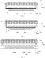
- FIG. 1 is a structural schematic view of a display panel according to an embodiment of the present disclosure.
- the display panel may be applied in various displaying manners, such as an OLED displaying, a quantum dot displaying, a micro-LED displaying, and the like.
- the display panel may include following components.
- a cover plate 10 may be arranged.
- the cover plate 10 may be a glass cover plate.
- the glass cover plate may have advantages of chemical stability, electrical insulation and compactness.
- a substrate 12 may be arranged and spaced apart from the cover plate 10. An edge of the substrate 12 may be connected to an edge of the cover plate 10 through an adhesive member 14.
- the substrate 12 may include a first region 120 enclosed and defined by the adhesive member 14.
- the substrate 12 may be a glass substrate.
- the glass substrate may have advantages of chemical stability, electrical insulation and compactness.
- An anode, an organic light emitting layer (such as an OLED element and the like), a cathode, and the like may be stacked sequentially and disposed between the substrate 12 and the cover plate 10. When the edge of the substrate 12 and the edge of the cover plate 10 are sealed by the adhesive member 14, a sealed space may be defined between the substrate 12 and the cover plate 10.
- the anode, the organic light emitting layer, and the cathode may be isolated from an external environment effectively to reduce a possibility of moisture corrosion.
- a supportive member may be disposed between the substrate 12 and the cover plate 10.
- the adhesive member 14 may be made of frit material.
- the frit material may typically include glass powder, filler, adhesive/resin, and the like. In other embodiments, the adhesive member 14 may be made of other types of material.
- a protective layer 16 may be arranged on a side of the substrate 12 away from the cover plate 10.
- An impact abruption structure 13 may be configured on the protective layer 16 or configured between the protective layer 16 and the adhesive member 14. The impact may be applied towards the substrate 12.
- a direction of the impact may extend from the substrate 12 to the cover plate 10; or the direction of the impact may be perpendicular to the substrate 12; or the direction of the impact may be inclined to the substrate 12, and an angle between the direction and a surface of the substrate 12 may be an acute angle.
- the impact may be weakened by the impact abruption structure 13, such that the impact reaching the adhesive member 14 may be reduced, a possibility of the adhesive member 14 being damaged may be reduced, and a capability of the display panel resistant against the impact while the panel dropping with a back of the panel facing the ground may be improved.
- the display panel may further include other components, such as a polarizing plate, disposed on a side of the cover plate 10 away from the substrate 12.
- a stage portion 18 may be formed between the protective layer 16 and the substrate 12.
- the stage portion 18 may include at least one side wall protruding from an outer surface 122 of the substrate 12.
- a side wall A will be taken as an example for description.
- An orthographic projection of the side wall A onto the substrate 12 may be located in the first region 120.
- the stage portion 18 may serve as the impact abruption structure 13.
- the stage portion 18 may be configured to allow a side of the substrate 12 to be covered by two protective layers 16 having different thicknesses. A thickness of the protective layer 16 corresponding to the first region 120 may be greater than that of the protective layer 16 corresponding to the adhesive member 14.
- the stage portion 18 may be configured to allow the protective layer 16 to have a mismatch at a position corresponding to the adhesive member 14.
- the protective layer 16 corresponding to the first region 120 may receive the impact directly, whereas the protective layer 16 or the substrate 12 at the position corresponding to the adhesive member 14 may not receive the impact directly, the adhesive member 14 may not be a direct impact point, such that the impact applied to the adhesive member 14 may be weakened to a large extent, and the capability of the display panel resistant against the impact may be improved.
- the above-mentioned means of enabling the stage portion 18 to serve as the impact abruption structure 13 may be achieved easily.
- the impact abruption structure 13 may be configured by other means.
- an air bag may be configured at a position of the protective layer 16 corresponding to the adhesive member 14 to buffer the impact reaching the adhesive member 14.
- the orthographic projection of the side wall A onto the substrate 12 may be located in the first region 120. There may be a distance d1 between the orthographic projection of the side wall A and an orthographic projection of the adhesive member 14 onto the substrate 12.
- the distance d1 may be in a range of 0.3mm to 5mm, such as 0.3mm, 2mm, 4mm, 5mm, and the like.
- the distance enables the adhesive member 14 not to be the direct impact point while the display panel dropping with the back facing the ground, and the adhesive member 14 may be impacted only if the substrate 12 vibrates transversely.
- the distance may reduce a possibility of the substrate 12 being damaged while dropping.
- FIG. 2 is a structural schematic view of a display panel according to another embodiment of the present disclosure.
- a stage portion 18a may include as least two side walls.
- side walls B and C will be taken as examples for illustration.
- Orthographic projections of the side walls B and C onto the substrate 12a may be located in the first region 120a.
- the distance d2 may be in a range of 0.3mm to 5mm, such as 0.3mm, 2mm, 4mm, 5mm, and the like.
- the present embodiment may have the same advantages as the embodiment mentioned in the above.
- the orthographic projection of the protective layer 16/16a onto the substrate 12/12a may be located in the first region 120/120a. That is, a thickness of the protective layer 16/16a at the position corresponding to the adhesive member 14/14a may be 0.
- the stage portion 18/18a may be formed by a side edge 160/160a of the protective layer 16/16a and the outer surface 122/122a of the substrate 12/12a.
- the number of stages included in the stage portion 18/18a may be one, two, three, and the like.
- the side edge 160a of the protective layer 16a may include a plurality of side walls, such as the side wall B, the side wall C, and a surface D connected to the side walls B and C.
- the protective layer 16/16a may be achieved easily.
- the protective layer 16/16a may be a cushion pad, such as a cushion foam, and the like. The cushion pad may further buffer the impact applied to the substrate 12/12a while the display panel dropping with the back facing the ground, such that the impact transferred through the substrate 12/12a reaching the adhesive member 14/14a may further be reduced.
- the display panel may further include a light-shielding sheet 11 disposed between the protective layer 16 and the substrate 12.
- the orthographic projection of the light-shielding sheet 11 onto the substrate 12 may at least extend to reach the adhesive member 14.
- the light-shielding sheet 11 may completely cover the substrate 12.
- the light-shielding sheet 11 may be made of non-transparent material, such as a black tape.
- the light-shielding sheet 11 may effectively reduce light leaking to a region of the substrate 12 uncovered by the protective layer 16.
- the protective layer 16 is made of the non-transparent material
- the light-shielding sheet 11 may be configured to cover a portion of the substrate 12 uncovered by the protective layer 16 only.
- FIG. 3 is a structural schematic view of a display panel according to still another embodiment of the present disclosure.
- the orthographic projection of the protective layer 16b onto the substrate 12b may at least completely cover the first region 120b. That is, the orthographic projection of the protective layer 16b onto the substrate 12b may not only cover the first region 120b, but also may cover a region out of the first region 120b. For example, the orthographic projection of the protective layer 16b onto the substrate 12b may completely cover the substrate 12b.
- the protective layer 16b may include a first layer 162b and a second layer 164b which are stacked together. The second layer 164b may be disposed between the first layer 162b and the substrate 12b.
- An area of the first layer 162b may be greater than that of the second layer 164b.
- An orthographic projection of the second layer 164b onto the substrate 12b may be located in the first region 120b.
- the stage portion 18b may be formed by a side edge 1640b of the second layer 164b and the outer surface 122b of the substrate 12b.
- the stage portion 18b formed by the above-mentioned means may be achieved easily.
- the first layer 162b and the second layer 164b of the protective layer 16b may be configured individually and may be connected via an adhesive element. By configuring the first and the second layers individually, assembling the display panel in a subsequent process may be performed easily.
- the first layer 162b and the second layer 164b may be integrally configured as an overall structure.
- the protective layer 16b may be formed by a proper mould or by a proper cutting process.
- the protective layer 16b may be the cushion pad, such as the cushion foam and the like. The cushion pad may further reduce the impact applied to the substrate 12b while the display panel dropping with the back facing the ground, such that the impact transferred through the substrate 12b reaching the adhesive member 14b may further be reduced.
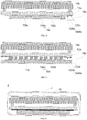
- FIG. 4 is a structural schematic view of a display panel according to still another embodiment of the present disclosure.
- the orthographic projection of the protective layer 16c onto the substrate 12c may at least completely cover the first region 120c and a region out of the first region 120c. That is, the orthographic projection of the protective layer 16c onto the substrate 12c may not only cover the first region 120c, but also may cover a region out of the first region 120c.
- the orthographic projection of the protective layer 16c onto the substrate 12c completely covers the substrate 12c.
- the protective layer 16c may include a first layer 162c and a second layer 164c which are stacked together. The second layer 164c may be disposed between the first layer 162c and the substrate 12c.
- An area of the first layer 162c may be less than that of the second layer 164c.
- An orthographic projection of the first layer 162c onto the substrate 12c may be located in the first region 120c.
- the stage portion 18c may be formed by a side edge 1620c of the first layer 162c, a side edge 1640c of the second layer 164c, and the outer surface 122c of the substrate 12c.
- the stage portion 18c formed by the above-mentioned means may be achieved easily.
- the first layer 162c and the second layer 164c of the protective layer 16c may be configured individually and may be connected via an adhesive element. By configuring the first and the second layers individually, assembling the display panel in a subsequent process may be performed easily.
- the first layer 162c and the second layer 164c may be integrally configured as an overall structure. That is, the protective layer 16c may be formed by a proper mould or by a proper cutting process. Further, in the present embodiment, the protective layer 16c may be the cushion pad, such as the cushion foam and the like. The cushion pad may further reduce the impact applied to the substrate 12c while the display panel dropping with the back facing the ground, such that the impact transferred through the substrate 12c reaching the adhesive member 14c may further be reduced.
- FIG. 5 is a structural schematic view of a display panel according to still another embodiment of the present disclosure.
- the protective layer 16d in the present embodiment may be a layer of coating, such as a coating of silicone dioxide sol and the like.
- the protective coating may improve surface intensity of the substrate 12d to reduce a possibility of the substrate 12d being cracked when receiving the impact.
- a structure of the protective layer 16d may be similar to that shown in FIGS. 1 to 4 .
- the protective layer 16d is configured as the one shown in FIGS.
- the display panel may further include a cushion pad 11d, disposed at a side of the protective coating away from the substrate 12d.
- the cushion pad 11d may further buffer the impact applied to the substrate 12d while the display panel dropping with the back facing the ground, such that the impact transferred through the substrate 12d reaching the adhesive member 14d may further be reduced.
- the protective coating on an outer side of the substrate 12d may serve as a stage portion 18d, and the stage portion 18d may protect the adhesive member 14d.
- the cushion pad in the present embodiment may not be required to be configured twice, such that complexity of assembling the display panel in a subsequent process may be reduced.
- a thickness of the protective coating shown in FIG. 5 may be uniform, and an orthographic projection of the protective coating onto the substrate may cover the substrate.
- a structure of the cushion pad disposed at a side of the protective coating may refer to that shown in FIGS. 1 to 4 .
- a test method that is performed includes: taking a jig to simulate the display panel dropping with the back facing the ground; and dropping the display panel respectively twice from a height of 0.7 meters, a height of 0.8 meters, and a height of 0.9 meters.
- the impact applied to the adhesive member may be reduced, a possibility of the adhesive member being damaged may be reduced, such that a capability of the display panel resistant against the external impact may be improved.
- FIG. 6 is a structural schematic view of a display apparatus according to an embodiment of the present disclosure.
- the display apparatus 2 may include the display panel 1 according to any one of the above embodiments and a shell 20 disposed at a periphery of the display panel 1.
- the display apparatus 2 may be a mobile phone, a computer, and the like.
- the impact transferred through the shell 20 to the adhesive member may be weakened by the impact abruption structure, such that the impact reaching the adhesive member may be reduced, a possibility of the adhesive member being damaged may be reduced, and the capability of the display apparatus 2 resistant against the impact may be improved.
Landscapes
- Physics & Mathematics (AREA)
- Optics & Photonics (AREA)
- Devices For Indicating Variable Information By Combining Individual Elements (AREA)
- Electroluminescent Light Sources (AREA)
Abstract
Description
- This application claims a priority of
Chinese Patent Application No.201910406923.X, filed on May 16, 2019 - The present disclosure generally relates to the technical field of displaying, and particularly to a display panel and a display apparatus.
- In the technical field of organic light emitting diode (Organic Light Emitting Didoe, referred to as OLED) displaying, in order to prevent moisture, oxygen, dust, and the like, from damaging an OLED element, a suitable form of packaging may be applied to isolate the OLED element from an external environment to improve service life of the OLED element.
- Glass frit packaging is a form of packaging that is often applied for an OLED hard screen. In detail, a substrate and a cover plate are spaced apart from each other, an edge of the substrate and an edge of the cover plate are sealed by the frit, and a space defined by the substrate and the cover plate are vacuum or filled with inert gas. In this way, the OLED element disposed between the substrate and the cover plate is isolated from the external environment.
- The applicant of the present disclosure discovered in long-term research that, since the substrate and the cover plate are substantially supported by the frit, when the display panel is dropped with a back of the display panel facing the ground, strength provided by the frit is insufficient, and the frit is easily damaged in response to an external impact, causing failure of the display panel.
- The present disclosure provides a display panel and a display apparatus to reduce a possibility of an adhesive element being damaged when the display panel is impacted.
- In a first aspect of the present disclosure, a display panel is provided and includes: a cover plate, a substrate, and a protective layer. The substrate is spaced apart from the cover plate. An edge of the substrate is connected to an edge of the cover plate through an adhesive member, and the substrate includes a first region enclosed by the adhesive member. The protective layer is disposed on a side of the substrate away from the cover plate. An impact abruption structure is configured on the protective layer or configured between the protective layer and the adhesive member, and an impact is applied towards the substrate.
- In a second aspect of the present disclosure, a display apparatus is provided and includes the display panel according to any one of the above embodiments and a shell disposed at a periphery of the display panel.
- According to the present disclosure, the display panel is configured with an impact abruption structure. The impact abruption structure may be disposed on the protective layer or disposed between the protective layer and the adhesive member. When the display panel receives an impact, and the impact applies towards the substrate, the impact may be weakened by the impact abruption structure, such that the impact reaching the adhesive member may be reduced, and a possibility of the adhesive member being damaged may be reduced, improving a capability of the display panel resistant against the impact while the panel dropping with a back of the panel facing the ground.
- In order to illustrate technical solutions of embodiments of the present disclosure more clearly, accompanying drawings required for illustrating the embodiments will be described in brief. Obviously, the following drawings show only some embodiments of the present disclosure, any ordinary skilled person in the art may obtain other drawings based on the following drawings without making any creative work.
-
FIG. 1 is a structural schematic view of a display panel according to an embodiment of the present disclosure. -
FIG. 2 is a structural schematic view of a display panel according to an embodiment of the present disclosure, where a stage portion includes two side walls. -
FIG. 3 is a structural schematic view of the display panel shown inFIG. 2 , where an orthographic projection of a protective layer onto a substrate at least completely covers a first region. -
FIG. 4 is a structural schematic view of the display panel shown inFIG. 3 , where the orthographic projection of the protective layer onto the substrate completely covers the substrate. -
FIG. 5 is a structural schematic view of the display panel shown inFIG. 1 , where the protective layer is a protective coating. -
FIG. 6 is a structural schematic view of a display apparatus according to an embodiment of the present disclosure. - The technical solutions according to the embodiments of the present application will be described clearly and completely by referring to the accompanying drawings of the embodiments of the present application. Obviously, the described embodiments are only a part of, but not all of, the embodiments of the present application. Based on the embodiments in the present disclosure, other embodiments may be obtained by any ordinary skilled person in the art without creative work, and the obtained other embodiments shall fall within the scope of the present disclosure.
- As shown in
FIG. 1, FIG. 1 is a structural schematic view of a display panel according to an embodiment of the present disclosure. The display panel may be applied in various displaying manners, such as an OLED displaying, a quantum dot displaying, a micro-LED displaying, and the like. The display panel may include following components. - A
cover plate 10 may be arranged. In the present embodiment, thecover plate 10 may be a glass cover plate. The glass cover plate may have advantages of chemical stability, electrical insulation and compactness. - A
substrate 12 may be arranged and spaced apart from thecover plate 10. An edge of thesubstrate 12 may be connected to an edge of thecover plate 10 through anadhesive member 14. Thesubstrate 12 may include afirst region 120 enclosed and defined by theadhesive member 14. In the present embodiment, thesubstrate 12 may be a glass substrate. The glass substrate may have advantages of chemical stability, electrical insulation and compactness. An anode, an organic light emitting layer (such as an OLED element and the like), a cathode, and the like may be stacked sequentially and disposed between thesubstrate 12 and thecover plate 10. When the edge of thesubstrate 12 and the edge of thecover plate 10 are sealed by theadhesive member 14, a sealed space may be defined between thesubstrate 12 and thecover plate 10. When the sealed space is vacuum or filled with inert gas, the anode, the organic light emitting layer, and the cathode may be isolated from an external environment effectively to reduce a possibility of moisture corrosion. In order to allow thesubstrate 12 to be spaced apart from thecover plate 10, a supportive member may be disposed between thesubstrate 12 and thecover plate 10. Further, theadhesive member 14 may be made of frit material. The frit material may typically include glass powder, filler, adhesive/resin, and the like. In other embodiments, theadhesive member 14 may be made of other types of material. - A
protective layer 16 may be arranged on a side of thesubstrate 12 away from thecover plate 10. An impact abruption structure 13 may be configured on theprotective layer 16 or configured between theprotective layer 16 and theadhesive member 14. The impact may be applied towards thesubstrate 12. For example, a direction of the impact may extend from thesubstrate 12 to thecover plate 10; or the direction of the impact may be perpendicular to thesubstrate 12; or the direction of the impact may be inclined to thesubstrate 12, and an angle between the direction and a surface of thesubstrate 12 may be an acute angle. When the display panel receives the impact that is applied towards thesubstrate 12, and when the direction of the impact extends from thesubstrate 12 to thecover plate 10, the impact may be weakened by the impact abruption structure 13, such that the impact reaching theadhesive member 14 may be reduced, a possibility of theadhesive member 14 being damaged may be reduced, and a capability of the display panel resistant against the impact while the panel dropping with a back of the panel facing the ground may be improved. - Further, in the present embodiment, the display panel may further include other components, such as a polarizing plate, disposed on a side of the
cover plate 10 away from thesubstrate 12. - In one embodiment, as shown in
FIG. 1 , a stage portion 18 may be formed between theprotective layer 16 and thesubstrate 12. The stage portion 18 may include at least one side wall protruding from anouter surface 122 of thesubstrate 12. In the present embodiment, a side wall A will be taken as an example for description. An orthographic projection of the side wall A onto thesubstrate 12 may be located in thefirst region 120. The stage portion 18 may serve as the impact abruption structure 13. The stage portion 18 may be configured to allow a side of thesubstrate 12 to be covered by twoprotective layers 16 having different thicknesses. A thickness of theprotective layer 16 corresponding to thefirst region 120 may be greater than that of theprotective layer 16 corresponding to theadhesive member 14. That is, the stage portion 18 may be configured to allow theprotective layer 16 to have a mismatch at a position corresponding to theadhesive member 14. When the display panel drops with the back of the display panel facing the ground, theprotective layer 16 corresponding to thefirst region 120 may receive the impact directly, whereas theprotective layer 16 or thesubstrate 12 at the position corresponding to theadhesive member 14 may not receive the impact directly, theadhesive member 14 may not be a direct impact point, such that the impact applied to theadhesive member 14 may be weakened to a large extent, and the capability of the display panel resistant against the impact may be improved. In addition, the above-mentioned means of enabling the stage portion 18 to serve as the impact abruption structure 13 may be achieved easily. In other embodiments, the impact abruption structure 13 may be configured by other means. For example, an air bag may be configured at a position of theprotective layer 16 corresponding to theadhesive member 14 to buffer the impact reaching theadhesive member 14. - In the present embodiment, as shown in
FIG. 1 , the orthographic projection of the side wall A onto thesubstrate 12 may be located in thefirst region 120. There may be a distance d1 between the orthographic projection of the side wall A and an orthographic projection of theadhesive member 14 onto thesubstrate 12. The distance d1 may be in a range of 0.3mm to 5mm, such as 0.3mm, 2mm, 4mm, 5mm, and the like. In one aspect, the distance enables theadhesive member 14 not to be the direct impact point while the display panel dropping with the back facing the ground, and theadhesive member 14 may be impacted only if thesubstrate 12 vibrates transversely. In another aspect, the distance may reduce a possibility of thesubstrate 12 being damaged while dropping. - In other embodiments, as shown in
FIG. 2, FIG. 2 is a structural schematic view of a display panel according to another embodiment of the present disclosure. Astage portion 18a may include as least two side walls. In the present embodiment, side walls B and C will be taken as examples for illustration. Orthographic projections of the side walls B and C onto thesubstrate 12a may be located in thefirst region 120a. In this situation, there may be a distance d2 between orthographic projection of the side wall C, which is adjacent to a center of the display panel at most, and an orthographic projection of theadhesive member 14a onto thesubstrate 12a. The distance d2 may be in a range of 0.3mm to 5mm, such as 0.3mm, 2mm, 4mm, 5mm, and the like. The present embodiment may have the same advantages as the embodiment mentioned in the above. - In one application scenario, as shown in
FIG. 1 and FIG. 2 , the orthographic projection of theprotective layer 16/16a onto thesubstrate 12/12a may be located in thefirst region 120/120a. That is, a thickness of theprotective layer 16/16a at the position corresponding to theadhesive member 14/14a may be 0. The stage portion 18/18a may be formed by aside edge 160/160a of theprotective layer 16/16a and theouter surface 122/122a of thesubstrate 12/12a. The number of stages included in the stage portion 18/18a may be one, two, three, and the like. When the number of stages included in thestage portion 18a is more than one, theside edge 160a of theprotective layer 16a may include a plurality of side walls, such as the side wall B, the side wall C, and a surface D connected to the side walls B and C. In this way, theprotective layer 16/16a may be achieved easily. Further, in the present embodiment, theprotective layer 16/16a may be a cushion pad, such as a cushion foam, and the like. The cushion pad may further buffer the impact applied to thesubstrate 12/12a while the display panel dropping with the back facing the ground, such that the impact transferred through thesubstrate 12/12a reaching theadhesive member 14/14a may further be reduced. - Further, in the present embodiment, as shown in
FIG. 1 , the display panel may further include a light-shieldingsheet 11 disposed between theprotective layer 16 and thesubstrate 12. The orthographic projection of the light-shieldingsheet 11 onto thesubstrate 12 may at least extend to reach theadhesive member 14. For example, the light-shieldingsheet 11 may completely cover thesubstrate 12. The light-shieldingsheet 11 may be made of non-transparent material, such as a black tape. The light-shieldingsheet 11 may effectively reduce light leaking to a region of thesubstrate 12 uncovered by theprotective layer 16. In other embodiments, when theprotective layer 16 is made of the non-transparent material, the light-shieldingsheet 11 may be configured to cover a portion of thesubstrate 12 uncovered by theprotective layer 16 only. - In another application scenario, as shown in
FIG. 3, FIG. 3 is a structural schematic view of a display panel according to still another embodiment of the present disclosure. The orthographic projection of theprotective layer 16b onto thesubstrate 12b may at least completely cover thefirst region 120b. That is, the orthographic projection of theprotective layer 16b onto thesubstrate 12b may not only cover thefirst region 120b, but also may cover a region out of thefirst region 120b. For example, the orthographic projection of theprotective layer 16b onto thesubstrate 12b may completely cover thesubstrate 12b. Theprotective layer 16b may include afirst layer 162b and asecond layer 164b which are stacked together. Thesecond layer 164b may be disposed between thefirst layer 162b and thesubstrate 12b. An area of thefirst layer 162b may be greater than that of thesecond layer 164b. An orthographic projection of thesecond layer 164b onto thesubstrate 12b may be located in thefirst region 120b. Thestage portion 18b may be formed by aside edge 1640b of thesecond layer 164b and theouter surface 122b of thesubstrate 12b. Thestage portion 18b formed by the above-mentioned means may be achieved easily. Thefirst layer 162b and thesecond layer 164b of theprotective layer 16b may be configured individually and may be connected via an adhesive element. By configuring the first and the second layers individually, assembling the display panel in a subsequent process may be performed easily. In other embodiments, thefirst layer 162b and thesecond layer 164b may be integrally configured as an overall structure. That is, theprotective layer 16b may be formed by a proper mould or by a proper cutting process. In addition, in the present embodiment, theprotective layer 16b may be the cushion pad, such as the cushion foam and the like. The cushion pad may further reduce the impact applied to thesubstrate 12b while the display panel dropping with the back facing the ground, such that the impact transferred through thesubstrate 12b reaching theadhesive member 14b may further be reduced. - In still another application scenario, as shown in
FIG. 4, FIG. 4 is a structural schematic view of a display panel according to still another embodiment of the present disclosure. The orthographic projection of theprotective layer 16c onto thesubstrate 12c may at least completely cover thefirst region 120c and a region out of thefirst region 120c. That is, the orthographic projection of theprotective layer 16c onto thesubstrate 12c may not only cover thefirst region 120c, but also may cover a region out of thefirst region 120c. For example, the orthographic projection of theprotective layer 16c onto thesubstrate 12c completely covers thesubstrate 12c. Theprotective layer 16c may include afirst layer 162c and asecond layer 164c which are stacked together. Thesecond layer 164c may be disposed between thefirst layer 162c and thesubstrate 12c. An area of thefirst layer 162c may be less than that of thesecond layer 164c. An orthographic projection of thefirst layer 162c onto thesubstrate 12c may be located in thefirst region 120c. Thestage portion 18c may be formed by aside edge 1620c of thefirst layer 162c, aside edge 1640c of thesecond layer 164c, and theouter surface 122c of thesubstrate 12c. Thestage portion 18c formed by the above-mentioned means may be achieved easily. Thefirst layer 162c and thesecond layer 164c of theprotective layer 16c may be configured individually and may be connected via an adhesive element. By configuring the first and the second layers individually, assembling the display panel in a subsequent process may be performed easily. In other embodiments, thefirst layer 162c and thesecond layer 164c may be integrally configured as an overall structure. That is, theprotective layer 16c may be formed by a proper mould or by a proper cutting process. Further, in the present embodiment, theprotective layer 16c may be the cushion pad, such as the cushion foam and the like. The cushion pad may further reduce the impact applied to thesubstrate 12c while the display panel dropping with the back facing the ground, such that the impact transferred through thesubstrate 12c reaching theadhesive member 14c may further be reduced. - In still another embodiment, as shown in
FIG. 5, FIG. 5 is a structural schematic view of a display panel according to still another embodiment of the present disclosure. Compared to the above embodiment, theprotective layer 16d in the present embodiment may be a layer of coating, such as a coating of silicone dioxide sol and the like. The protective coating may improve surface intensity of thesubstrate 12d to reduce a possibility of thesubstrate 12d being cracked when receiving the impact. A structure of theprotective layer 16d may be similar to that shown inFIGS. 1 to 4 . When theprotective layer 16d is configured as the one shown inFIGS. 3 and4 , that is when theprotective layer 16d includes afirst layer 162d and asecond layer 164d, a step-by-step coating may be performed to obtain thefirst layer 162d and thesecond layer 164d. Further, in the present embodiment, the display panel may further include acushion pad 11d, disposed at a side of the protective coating away from thesubstrate 12d. Thecushion pad 11d may further buffer the impact applied to thesubstrate 12d while the display panel dropping with the back facing the ground, such that the impact transferred through thesubstrate 12d reaching theadhesive member 14d may further be reduced. In the present embodiment, the protective coating on an outer side of thesubstrate 12d may serve as astage portion 18d, and thestage portion 18d may protect theadhesive member 14d. Compared to the embodiments shown inFIG. 3 andFIG. 4 , the cushion pad in the present embodiment may not be required to be configured twice, such that complexity of assembling the display panel in a subsequent process may be reduced. - In other embodiments, a thickness of the protective coating shown in
FIG. 5 may be uniform, and an orthographic projection of the protective coating onto the substrate may cover the substrate. A structure of the cushion pad disposed at a side of the protective coating may refer to that shown inFIGS. 1 to 4 . - Specific experimental data will be described in the following to verify the display panel provided in the present disclosure.
- A test method that is performed includes: taking a jig to simulate the display panel dropping with the back facing the ground; and dropping the display panel respectively twice from a height of 0.7 meters, a height of 0.8 meters, and a height of 0.9 meters.
- When the display panels in the art drop with the back facing the ground from the height of 0.7m, 4 out of 5 display panels are broken. When the display panels provided in the present disclosure drop with the back facing the ground from the height of 0.7m, 0 out of 5 display panels are broken. When the display panels provided in the present disclosure drop with the back facing the ground from the height of 0.8m, 0 out of 5 display panels are broken. When the display panels provided in the present disclosure drop with the back facing the ground from the height of 0.9m, 5 out of 5 display panels are broken.
- According to the above test results, when the display panel provided in the present disclosure drops with the back facing the ground, the impact applied to the adhesive member may be reduced, a possibility of the adhesive member being damaged may be reduced, such that a capability of the display panel resistant against the external impact may be improved.
- As shown in
FIG. 6, FIG. 6 is a structural schematic view of a display apparatus according to an embodiment of the present disclosure. Thedisplay apparatus 2 may include thedisplay panel 1 according to any one of the above embodiments and ashell 20 disposed at a periphery of thedisplay panel 1. Thedisplay apparatus 2 may be a mobile phone, a computer, and the like. When thedisplay apparatus 2 drops with the back facing the ground, the impact transferred through theshell 20 to the adhesive member may be weakened by the impact abruption structure, such that the impact reaching the adhesive member may be reduced, a possibility of the adhesive member being damaged may be reduced, and the capability of thedisplay apparatus 2 resistant against the impact may be improved. - The above description shows only embodiments of the present disclosure, and does not limit the scope of the present disclosure. Any equivalent structure or equivalent process transformation made based on the content of the present description and drawings, directly or indirectly applied to other related art, should be included in the scope of the present disclosure.
Claims (15)
- A display panel, comprising:a cover plate;a substrate, spaced apart from the cover plate, an edge of the substrate being connected to an edge of the cover plate through an adhesive member, and the substrate comprising a first region enclosed by the adhesive member; anda protective layer, disposed on a side of the substrate away from the cover plate;wherein an impact abruption structure is configured on the protective layer or configured between the protective layer and the adhesive member, and an impact is applied towards the substrate.
- The display panel according to claim 1, wherein a stage portion serves as the impact abruption structure and is configured between the protective layer and the substrate;
the stage portion comprises at least one side wall protruding from an outer surface of the substrate; and an orthographic projection of the at least one side wall onto the substrate is located in the first region. - The display panel according to claim 2, whereinthe stage portion comprises one side wall, an orthographic projection of the one side wall onto the substrate is located in the first region;a distance between the orthographic projection of the one side wall onto the substrate and an orthographic projection of the adhesive member onto the substrate is in a range from 0.3mm to 5mm.
- The display panel according to claim 2, whereinthe stage portion comprises at least two side walls, orthographic projections of the at least two side walls onto the substrate are located in the first region;a distance between the orthographic projection of one of the at least two side walls closest to a center of the display panel onto the substrate and an orthographic projection of the adhesive member onto the substrate is in a range from 0.3mm to 5mm.
- The display panel according to claim 2, whereinan orthographic projection of the protective layer onto the substrate is located in the first region; andthe stage portion comprises a side edge of the protective layer and the outer surface of the substrate.
- The display panel according to claim 5, further comprising a light-shielding sheet disposed between the protective layer and the substrate, wherein an orthographic projection of the light-shielding sheet onto the substrate at least extends to reach the adhesive member.
- The display panel according to claim 6, wherein the light-shielding sheet completely covers the substrate.
- The display panel according to claim 2, whereinan orthographic projection of the protective layer onto the substrate at least completely covers the first region;the protective layer comprises a first layer and a second layer which are stacked together, the second layer is disposed between the first layer and the substrate;an area of the first layer is greater than an area of the second layer;an orthographic projection of the second layer onto the substrate is located in the first region; andthe second layer and the outer surface of the substrate forms the stage portion.
- The display panel according to claim 2, whereinan orthographic projection of the protective layer onto the substrate at least completely covers the first region;the protective layer comprises a first layer and a second layer which are stacked together, the second layer is disposed between the first layer and the substrate;an area of the first layer is less than an area of the second layer;an orthographic projection of the first layer onto the substrate is located in the first region; andthe first layer, the second layer, and the outer surface of the substrate forms the stage portion.
- The display panel according to claim 8 or claim 9, wherein
the first layer and the second layer are configured as individual components and are connected via an adhesive element. - The display panel according to claim 8 or claim 9, wherein the first layer and the second layer are integrally configured as an overall structure.
- The display panel according to any one of claims 1 to 9, wherein the protective layer is a cushion pad.
- The display panel according to any one of claims 1 to 9, wherein the protective layer is a protective coating, the display panel further comprises a cushion pad, and the cushion pad is disposed at a side of the protective coating away from the substrate.
- The display panel according to claim 1, wherein an air bag is configured at a position of the protective layer corresponding to the adhesive member, and the air bag serves as the impact abruption structure.
- A display apparatus, comprising the display panel according to any one of claims 1 to 14 and a shell disposed at a periphery of the display panel.
Applications Claiming Priority (2)
| Application Number | Priority Date | Filing Date | Title |
|---|---|---|---|
| CN201910406923.XA CN110190032B (en) | 2019-05-16 | 2019-05-16 | A display panel and display device |
| PCT/CN2019/118928 WO2020228290A1 (en) | 2019-05-16 | 2019-11-15 | Display panel and display apparatus |
Publications (3)
| Publication Number | Publication Date |
|---|---|
| EP3896725A1 true EP3896725A1 (en) | 2021-10-20 |
| EP3896725A4 EP3896725A4 (en) | 2022-05-04 |
| EP3896725B1 EP3896725B1 (en) | 2024-12-25 |
Family
ID=67716544
Family Applications (1)
| Application Number | Title | Priority Date | Filing Date |
|---|---|---|---|
| EP19928833.3A Active EP3896725B1 (en) | 2019-05-16 | 2019-11-15 | Display panel and display apparatus |
Country Status (7)
| Country | Link |
|---|---|
| US (1) | US12063807B2 (en) |
| EP (1) | EP3896725B1 (en) |
| JP (1) | JP7105379B2 (en) |
| KR (1) | KR102601517B1 (en) |
| CN (1) | CN110190032B (en) |
| TW (1) | TWI713217B (en) |
| WO (1) | WO2020228290A1 (en) |
Families Citing this family (6)
| Publication number | Priority date | Publication date | Assignee | Title |
|---|---|---|---|---|
| CN110190032B (en) * | 2019-05-16 | 2020-07-03 | 昆山国显光电有限公司 | A display panel and display device |
| US20210257582A1 (en) * | 2020-02-14 | 2021-08-19 | Samsung Display Co., Ltd. | Display device |
| CN114039011B (en) * | 2021-10-19 | 2023-07-28 | 昆山国显光电有限公司 | Display device |
| CN114464753B (en) | 2022-01-19 | 2023-10-31 | 武汉华星光电半导体显示技术有限公司 | Display panel and cover plate assembly |
| CN115188267B (en) * | 2022-06-22 | 2023-10-20 | 广州国显科技有限公司 | Spacer block, method for manufacturing display device, and display device |
| CN119910992A (en) * | 2024-09-25 | 2025-05-02 | 北京小米移动软件有限公司 | Processing technology of panel module and panel module |
Family Cites Families (22)
| Publication number | Priority date | Publication date | Assignee | Title |
|---|---|---|---|---|
| US9101005B2 (en) * | 2009-09-15 | 2015-08-04 | Industrial Technology Research Institute | Package of environmental sensitive element |
| KR101690146B1 (en) * | 2010-09-02 | 2016-12-28 | 삼성디스플레이 주식회사 | Organic light emitting display device and method of manufacturing thereof |
| KR101940186B1 (en) * | 2012-10-29 | 2019-01-21 | 삼성디스플레이 주식회사 | Organic light emitting diode display |
| US9379355B1 (en) * | 2014-12-15 | 2016-06-28 | Lg Display Co., Ltd. | Flexible display device having support layer with rounded edge |
| CN105975128A (en) * | 2016-05-04 | 2016-09-28 | 武汉华星光电技术有限公司 | External-mounting touch display device and electronic equipment |
| CN105955533A (en) * | 2016-05-04 | 2016-09-21 | 武汉华星光电技术有限公司 | Outer-hanging touch display device with pressure-sensing touch function |
| CN107464824B (en) * | 2016-06-03 | 2020-02-21 | 上海和辉光电有限公司 | Display panel |
| KR102532769B1 (en) * | 2016-06-10 | 2023-05-17 | 삼성디스플레이 주식회사 | Display device |
| KR102533079B1 (en) * | 2016-08-04 | 2023-05-18 | 삼성디스플레이 주식회사 | Apparatus for sensing touch pressure |
| JP2018036514A (en) | 2016-08-31 | 2018-03-08 | 株式会社ジャパンディスプレイ | Display device |
| KR102564349B1 (en) * | 2016-09-30 | 2023-08-04 | 엘지디스플레이 주식회사 | Organic light emitting display apparatus |
| CN108345400A (en) * | 2017-01-22 | 2018-07-31 | 京东方科技集团股份有限公司 | Display base plate and display device |
| CN106990582A (en) | 2017-03-30 | 2017-07-28 | 武汉华星光电技术有限公司 | Liquid crystal display device |
| CN109037468A (en) * | 2017-06-09 | 2018-12-18 | 上海和辉光电有限公司 | A kind of display panel |
| CN107563306A (en) * | 2017-08-11 | 2018-01-09 | 维沃移动通信有限公司 | A kind of display module and terminal device |
| CN207381435U (en) | 2017-08-23 | 2018-05-18 | 上海和辉光电有限公司 | A kind of OLED display modules |
| JP2019049936A (en) | 2017-09-12 | 2019-03-28 | キヤノン電子株式会社 | Display unit structure |
| US10739630B2 (en) * | 2017-10-31 | 2020-08-11 | Wuhan China Star Optoelectronics Technology Co., Ltd. | Touch display panel and touch display device |
| CN108281566B (en) * | 2018-01-03 | 2020-04-10 | 深圳市华星光电半导体显示技术有限公司 | OLED panel and manufacturing method thereof |
| CN109119549B (en) * | 2018-08-28 | 2021-04-23 | 广州国显科技有限公司 | Display panel, display device and preparation method thereof |
| CN109782951B (en) * | 2019-01-09 | 2021-08-27 | 京东方科技集团股份有限公司 | Touch display panel and display device |
| CN110190032B (en) * | 2019-05-16 | 2020-07-03 | 昆山国显光电有限公司 | A display panel and display device |
-
2019
- 2019-05-16 CN CN201910406923.XA patent/CN110190032B/en active Active
- 2019-11-15 JP JP2021539891A patent/JP7105379B2/en active Active
- 2019-11-15 KR KR1020217020587A patent/KR102601517B1/en active Active
- 2019-11-15 WO PCT/CN2019/118928 patent/WO2020228290A1/en not_active Ceased
- 2019-11-15 EP EP19928833.3A patent/EP3896725B1/en active Active
- 2019-11-22 TW TW108142624A patent/TWI713217B/en active
-
2021
- 2021-06-02 US US17/337,263 patent/US12063807B2/en active Active
Also Published As
| Publication number | Publication date |
|---|---|
| KR20210091325A (en) | 2021-07-21 |
| WO2020228290A1 (en) | 2020-11-19 |
| US20210288288A1 (en) | 2021-09-16 |
| TW202017173A (en) | 2020-05-01 |
| KR102601517B1 (en) | 2023-11-14 |
| CN110190032B (en) | 2020-07-03 |
| TWI713217B (en) | 2020-12-11 |
| EP3896725A4 (en) | 2022-05-04 |
| US12063807B2 (en) | 2024-08-13 |
| JP7105379B2 (en) | 2022-07-22 |
| CN110190032A (en) | 2019-08-30 |
| EP3896725B1 (en) | 2024-12-25 |
| JP2022516674A (en) | 2022-03-01 |
Similar Documents
| Publication | Publication Date | Title |
|---|---|---|
| US12063807B2 (en) | Protection structure of display panel and display device | |
| US10510987B2 (en) | Display panel and manufacturing method therefor, and display device | |
| US20260076033A1 (en) | Display Panel and Manufacturing Method Therefor, Display Screen, and Electronic Device | |
| US8760365B2 (en) | Multi-display apparatus and method thereof | |
| US20210405801A1 (en) | Display panel and display device | |
| CN114333600B (en) | Display panel, preparation method of display panel and display module | |
| US12504623B2 (en) | Display panel and display apparatus | |
| US11825681B2 (en) | Display panel and display device | |
| CN111315173B (en) | Cover plate, display panel and display terminal | |
| JP2008077027A (en) | Organic electroluminescence display | |
| CN115050793B (en) | Display panel | |
| US11445278B2 (en) | Display panel buffering structure, display screen module and manufacturing method therefor, and terminal device | |
| US20250008821A1 (en) | Display module and method for manufacturing the same, polarizer assembly, and display apparatus | |
| US11482032B2 (en) | Display device and assembly method thereof | |
| CN116456752A (en) | Display panel, preparation method thereof and display device | |
| KR20230170111A (en) | Display panels and display devices | |
| US20180217442A1 (en) | Display panel and display device | |
| CN113097418B (en) | Display panel, manufacturing method of display panel and display device | |
| US10749145B2 (en) | Screen plate, packaging method, display panel and display device | |
| JP2002008853A (en) | Organic EL panel | |
| CN113764498A (en) | Cover plate assembly, display panel and display device | |
| KR20210067291A (en) | Display panel and manufacturing method of the same | |
| JP2002216948A (en) | Organic el panel | |
| CN120751902A (en) | Display panel and electronic device | |
| CN114039011A (en) | Display device |
Legal Events
| Date | Code | Title | Description |
|---|---|---|---|
| STAA | Information on the status of an ep patent application or granted ep patent |
Free format text: STATUS: THE INTERNATIONAL PUBLICATION HAS BEEN MADE |
|
| PUAI | Public reference made under article 153(3) epc to a published international application that has entered the european phase |
Free format text: ORIGINAL CODE: 0009012 |
|
| STAA | Information on the status of an ep patent application or granted ep patent |
Free format text: STATUS: REQUEST FOR EXAMINATION WAS MADE |
|
| 17P | Request for examination filed |
Effective date: 20210715 |
|
| AK | Designated contracting states |
Kind code of ref document: A1 Designated state(s): AL AT BE BG CH CY CZ DE DK EE ES FI FR GB GR HR HU IE IS IT LI LT LU LV MC MK MT NL NO PL PT RO RS SE SI SK SM TR |
|
| A4 | Supplementary search report drawn up and despatched |
Effective date: 20220407 |
|
| RIC1 | Information provided on ipc code assigned before grant |
Ipc: H01L 51/52 20060101ALI20220401BHEP Ipc: H01L 23/00 20060101AFI20220401BHEP |
|
| DAV | Request for validation of the european patent (deleted) | ||
| DAX | Request for extension of the european patent (deleted) | ||
| REG | Reference to a national code |
Ref country code: DE Free format text: PREVIOUS MAIN CLASS: H01L0023000000 Ipc: H10K0050844000 Ref country code: DE Ref legal event code: R079 Ref document number: 602019064109 Country of ref document: DE Free format text: PREVIOUS MAIN CLASS: H01L0023000000 Ipc: H10K0050844000 |
|
| GRAP | Despatch of communication of intention to grant a patent |
Free format text: ORIGINAL CODE: EPIDOSNIGR1 |
|
| STAA | Information on the status of an ep patent application or granted ep patent |
Free format text: STATUS: GRANT OF PATENT IS INTENDED |
|
| RIC1 | Information provided on ipc code assigned before grant |
Ipc: H10K 50/844 20230101AFI20240920BHEP |
|
| GRAS | Grant fee paid |
Free format text: ORIGINAL CODE: EPIDOSNIGR3 |
|
| INTG | Intention to grant announced |
Effective date: 20241018 |
|
| GRAA | (expected) grant |
Free format text: ORIGINAL CODE: 0009210 |
|
| STAA | Information on the status of an ep patent application or granted ep patent |
Free format text: STATUS: THE PATENT HAS BEEN GRANTED |
|
| AK | Designated contracting states |
Kind code of ref document: B1 Designated state(s): AL AT BE BG CH CY CZ DE DK EE ES FI FR GB GR HR HU IE IS IT LI LT LU LV MC MK MT NL NO PL PT RO RS SE SI SK SM TR |
|
| REG | Reference to a national code |
Ref country code: GB Ref legal event code: FG4D |
|
| REG | Reference to a national code |
Ref country code: CH Ref legal event code: EP |
|
| REG | Reference to a national code |
Ref country code: DE Ref legal event code: R096 Ref document number: 602019064109 Country of ref document: DE |
|
| REG | Reference to a national code |
Ref country code: IE Ref legal event code: FG4D |
|
| REG | Reference to a national code |
Ref country code: LT Ref legal event code: MG9D |
|
| PG25 | Lapsed in a contracting state [announced via postgrant information from national office to epo] |
Ref country code: HR Free format text: LAPSE BECAUSE OF FAILURE TO SUBMIT A TRANSLATION OF THE DESCRIPTION OR TO PAY THE FEE WITHIN THE PRESCRIBED TIME-LIMIT Effective date: 20241225 |
|
| PG25 | Lapsed in a contracting state [announced via postgrant information from national office to epo] |
Ref country code: FI Free format text: LAPSE BECAUSE OF FAILURE TO SUBMIT A TRANSLATION OF THE DESCRIPTION OR TO PAY THE FEE WITHIN THE PRESCRIBED TIME-LIMIT Effective date: 20241225 |
|
| PG25 | Lapsed in a contracting state [announced via postgrant information from national office to epo] |
Ref country code: BG Free format text: LAPSE BECAUSE OF FAILURE TO SUBMIT A TRANSLATION OF THE DESCRIPTION OR TO PAY THE FEE WITHIN THE PRESCRIBED TIME-LIMIT Effective date: 20241225 |
|
| PG25 | Lapsed in a contracting state [announced via postgrant information from national office to epo] |
Ref country code: NO Free format text: LAPSE BECAUSE OF FAILURE TO SUBMIT A TRANSLATION OF THE DESCRIPTION OR TO PAY THE FEE WITHIN THE PRESCRIBED TIME-LIMIT Effective date: 20250325 |
|
| PG25 | Lapsed in a contracting state [announced via postgrant information from national office to epo] |
Ref country code: LV Free format text: LAPSE BECAUSE OF FAILURE TO SUBMIT A TRANSLATION OF THE DESCRIPTION OR TO PAY THE FEE WITHIN THE PRESCRIBED TIME-LIMIT Effective date: 20241225 Ref country code: GR Free format text: LAPSE BECAUSE OF FAILURE TO SUBMIT A TRANSLATION OF THE DESCRIPTION OR TO PAY THE FEE WITHIN THE PRESCRIBED TIME-LIMIT Effective date: 20250326 |
|
| PG25 | Lapsed in a contracting state [announced via postgrant information from national office to epo] |
Ref country code: RS Free format text: LAPSE BECAUSE OF FAILURE TO SUBMIT A TRANSLATION OF THE DESCRIPTION OR TO PAY THE FEE WITHIN THE PRESCRIBED TIME-LIMIT Effective date: 20250325 |
|
| REG | Reference to a national code |
Ref country code: NL Ref legal event code: MP Effective date: 20241225 |
|
| PG25 | Lapsed in a contracting state [announced via postgrant information from national office to epo] |
Ref country code: NL Free format text: LAPSE BECAUSE OF FAILURE TO SUBMIT A TRANSLATION OF THE DESCRIPTION OR TO PAY THE FEE WITHIN THE PRESCRIBED TIME-LIMIT Effective date: 20241225 |
|
| REG | Reference to a national code |
Ref country code: AT Ref legal event code: MK05 Ref document number: 1755259 Country of ref document: AT Kind code of ref document: T Effective date: 20241225 |
|
| PG25 | Lapsed in a contracting state [announced via postgrant information from national office to epo] |
Ref country code: SM Free format text: LAPSE BECAUSE OF FAILURE TO SUBMIT A TRANSLATION OF THE DESCRIPTION OR TO PAY THE FEE WITHIN THE PRESCRIBED TIME-LIMIT Effective date: 20241225 |
|
| PG25 | Lapsed in a contracting state [announced via postgrant information from national office to epo] |
Ref country code: PL Free format text: LAPSE BECAUSE OF FAILURE TO SUBMIT A TRANSLATION OF THE DESCRIPTION OR TO PAY THE FEE WITHIN THE PRESCRIBED TIME-LIMIT Effective date: 20241225 |
|
| PG25 | Lapsed in a contracting state [announced via postgrant information from national office to epo] |
Ref country code: ES Free format text: LAPSE BECAUSE OF FAILURE TO SUBMIT A TRANSLATION OF THE DESCRIPTION OR TO PAY THE FEE WITHIN THE PRESCRIBED TIME-LIMIT Effective date: 20241225 |
|
| PG25 | Lapsed in a contracting state [announced via postgrant information from national office to epo] |
Ref country code: IS Free format text: LAPSE BECAUSE OF FAILURE TO SUBMIT A TRANSLATION OF THE DESCRIPTION OR TO PAY THE FEE WITHIN THE PRESCRIBED TIME-LIMIT Effective date: 20250425 |
|
| PG25 | Lapsed in a contracting state [announced via postgrant information from national office to epo] |
Ref country code: PT Free format text: LAPSE BECAUSE OF FAILURE TO SUBMIT A TRANSLATION OF THE DESCRIPTION OR TO PAY THE FEE WITHIN THE PRESCRIBED TIME-LIMIT Effective date: 20250428 |
|
| PG25 | Lapsed in a contracting state [announced via postgrant information from national office to epo] |
Ref country code: EE Free format text: LAPSE BECAUSE OF FAILURE TO SUBMIT A TRANSLATION OF THE DESCRIPTION OR TO PAY THE FEE WITHIN THE PRESCRIBED TIME-LIMIT Effective date: 20241225 |
|
| PG25 | Lapsed in a contracting state [announced via postgrant information from national office to epo] |
Ref country code: AT Free format text: LAPSE BECAUSE OF FAILURE TO SUBMIT A TRANSLATION OF THE DESCRIPTION OR TO PAY THE FEE WITHIN THE PRESCRIBED TIME-LIMIT Effective date: 20241225 Ref country code: RO Free format text: LAPSE BECAUSE OF FAILURE TO SUBMIT A TRANSLATION OF THE DESCRIPTION OR TO PAY THE FEE WITHIN THE PRESCRIBED TIME-LIMIT Effective date: 20241225 |
|
| PG25 | Lapsed in a contracting state [announced via postgrant information from national office to epo] |
Ref country code: SK Free format text: LAPSE BECAUSE OF FAILURE TO SUBMIT A TRANSLATION OF THE DESCRIPTION OR TO PAY THE FEE WITHIN THE PRESCRIBED TIME-LIMIT Effective date: 20241225 |
|
| PG25 | Lapsed in a contracting state [announced via postgrant information from national office to epo] |
Ref country code: CZ Free format text: LAPSE BECAUSE OF FAILURE TO SUBMIT A TRANSLATION OF THE DESCRIPTION OR TO PAY THE FEE WITHIN THE PRESCRIBED TIME-LIMIT Effective date: 20241225 |
|
| PG25 | Lapsed in a contracting state [announced via postgrant information from national office to epo] |
Ref country code: IT Free format text: LAPSE BECAUSE OF FAILURE TO SUBMIT A TRANSLATION OF THE DESCRIPTION OR TO PAY THE FEE WITHIN THE PRESCRIBED TIME-LIMIT Effective date: 20241225 |
|
| PG25 | Lapsed in a contracting state [announced via postgrant information from national office to epo] |
Ref country code: SE Free format text: LAPSE BECAUSE OF FAILURE TO SUBMIT A TRANSLATION OF THE DESCRIPTION OR TO PAY THE FEE WITHIN THE PRESCRIBED TIME-LIMIT Effective date: 20241225 |
|
| REG | Reference to a national code |
Ref country code: DE Ref legal event code: R097 Ref document number: 602019064109 Country of ref document: DE |
|
| PG25 | Lapsed in a contracting state [announced via postgrant information from national office to epo] |
Ref country code: DK Free format text: LAPSE BECAUSE OF FAILURE TO SUBMIT A TRANSLATION OF THE DESCRIPTION OR TO PAY THE FEE WITHIN THE PRESCRIBED TIME-LIMIT Effective date: 20241225 |
|
| PLBE | No opposition filed within time limit |
Free format text: ORIGINAL CODE: 0009261 |
|
| STAA | Information on the status of an ep patent application or granted ep patent |
Free format text: STATUS: NO OPPOSITION FILED WITHIN TIME LIMIT |
|
| 26N | No opposition filed |
Effective date: 20250926 |
|
| PGFP | Annual fee paid to national office [announced via postgrant information from national office to epo] |
Ref country code: DE Payment date: 20251117 Year of fee payment: 7 |