EP3896693A1 - Memory and addressing method therefor - Google Patents
Memory and addressing method therefor Download PDFInfo
- Publication number
- EP3896693A1 EP3896693A1 EP19947164.0A EP19947164A EP3896693A1 EP 3896693 A1 EP3896693 A1 EP 3896693A1 EP 19947164 A EP19947164 A EP 19947164A EP 3896693 A1 EP3896693 A1 EP 3896693A1
- Authority
- EP
- European Patent Office
- Prior art keywords
- address
- decoding
- unit
- memory
- input
- Prior art date
- Legal status (The legal status is an assumption and is not a legal conclusion. Google has not performed a legal analysis and makes no representation as to the accuracy of the status listed.)
- Granted
Links
Images


Classifications
-
- G—PHYSICS
- G11—INFORMATION STORAGE
- G11C—STATIC STORES
- G11C15/00—Digital stores in which information comprising one or more characteristic parts is written into the store and in which information is read-out by searching for one or more of these characteristic parts, i.e. associative or content-addressed stores
- G11C15/04—Digital stores in which information comprising one or more characteristic parts is written into the store and in which information is read-out by searching for one or more of these characteristic parts, i.e. associative or content-addressed stores using semiconductor elements
-
- G—PHYSICS
- G11—INFORMATION STORAGE
- G11C—STATIC STORES
- G11C29/00—Checking stores for correct operation ; Subsequent repair; Testing stores during standby or offline operation
- G11C29/04—Detection or location of defective memory elements, e.g. cell constructio details, timing of test signals
- G11C29/08—Functional testing, e.g. testing during refresh, power-on self testing [POST] or distributed testing
- G11C29/12—Built-in arrangements for testing, e.g. built-in self testing [BIST] or interconnection details
- G11C29/18—Address generation devices; Devices for accessing memories, e.g. details of addressing circuits
- G11C29/24—Accessing extra cells, e.g. dummy cells or redundant cells
-
- G—PHYSICS
- G11—INFORMATION STORAGE
- G11C—STATIC STORES
- G11C29/00—Checking stores for correct operation ; Subsequent repair; Testing stores during standby or offline operation
- G11C29/04—Detection or location of defective memory elements, e.g. cell constructio details, timing of test signals
- G11C29/08—Functional testing, e.g. testing during refresh, power-on self testing [POST] or distributed testing
- G11C29/10—Test algorithms, e.g. memory scan [MScan] algorithms; Test patterns, e.g. checkerboard patterns
-
- G—PHYSICS
- G11—INFORMATION STORAGE
- G11C—STATIC STORES
- G11C11/00—Digital stores characterised by the use of particular electric or magnetic storage elements; Storage elements therefor
- G11C11/21—Digital stores characterised by the use of particular electric or magnetic storage elements; Storage elements therefor using electric elements
- G11C11/34—Digital stores characterised by the use of particular electric or magnetic storage elements; Storage elements therefor using electric elements using semiconductor devices
- G11C11/40—Digital stores characterised by the use of particular electric or magnetic storage elements; Storage elements therefor using electric elements using semiconductor devices using transistors
- G11C11/401—Digital stores characterised by the use of particular electric or magnetic storage elements; Storage elements therefor using electric elements using semiconductor devices using transistors forming cells needing refreshing or charge regeneration, i.e. dynamic cells
- G11C11/4063—Auxiliary circuits, e.g. for addressing, decoding, driving, writing, sensing or timing
- G11C11/407—Auxiliary circuits, e.g. for addressing, decoding, driving, writing, sensing or timing for memory cells of the field-effect type
- G11C11/408—Address circuits
-
- G—PHYSICS
- G11—INFORMATION STORAGE
- G11C—STATIC STORES
- G11C11/00—Digital stores characterised by the use of particular electric or magnetic storage elements; Storage elements therefor
- G11C11/21—Digital stores characterised by the use of particular electric or magnetic storage elements; Storage elements therefor using electric elements
- G11C11/34—Digital stores characterised by the use of particular electric or magnetic storage elements; Storage elements therefor using electric elements using semiconductor devices
- G11C11/40—Digital stores characterised by the use of particular electric or magnetic storage elements; Storage elements therefor using electric elements using semiconductor devices using transistors
- G11C11/401—Digital stores characterised by the use of particular electric or magnetic storage elements; Storage elements therefor using electric elements using semiconductor devices using transistors forming cells needing refreshing or charge regeneration, i.e. dynamic cells
- G11C11/4063—Auxiliary circuits, e.g. for addressing, decoding, driving, writing, sensing or timing
- G11C11/407—Auxiliary circuits, e.g. for addressing, decoding, driving, writing, sensing or timing for memory cells of the field-effect type
- G11C11/408—Address circuits
- G11C11/4087—Address decoders, e.g. bit - or word line decoders; Multiple line decoders
-
- G—PHYSICS
- G11—INFORMATION STORAGE
- G11C—STATIC STORES
- G11C29/00—Checking stores for correct operation ; Subsequent repair; Testing stores during standby or offline operation
- G11C29/04—Detection or location of defective memory elements, e.g. cell constructio details, timing of test signals
- G11C29/08—Functional testing, e.g. testing during refresh, power-on self testing [POST] or distributed testing
- G11C29/12—Built-in arrangements for testing, e.g. built-in self testing [BIST] or interconnection details
- G11C29/18—Address generation devices; Devices for accessing memories, e.g. details of addressing circuits
-
- G—PHYSICS
- G11—INFORMATION STORAGE
- G11C—STATIC STORES
- G11C29/00—Checking stores for correct operation ; Subsequent repair; Testing stores during standby or offline operation
- G11C29/04—Detection or location of defective memory elements, e.g. cell constructio details, timing of test signals
- G11C29/08—Functional testing, e.g. testing during refresh, power-on self testing [POST] or distributed testing
- G11C29/12—Built-in arrangements for testing, e.g. built-in self testing [BIST] or interconnection details
- G11C29/36—Data generation devices, e.g. data inverters
-
- G—PHYSICS
- G11—INFORMATION STORAGE
- G11C—STATIC STORES
- G11C29/00—Checking stores for correct operation ; Subsequent repair; Testing stores during standby or offline operation
- G11C29/70—Masking faults in memories by using spares or by reconfiguring
- G11C29/76—Masking faults in memories by using spares or by reconfiguring using address translation or modifications
-
- G—PHYSICS
- G11—INFORMATION STORAGE
- G11C—STATIC STORES
- G11C7/00—Arrangements for writing information into, or reading information out from, a digital store
- G11C7/10—Input/output [I/O] data interface arrangements, e.g. I/O data control circuits, I/O data buffers
- G11C7/1006—Data managing, e.g. manipulating data before writing or reading out, data bus switches or control circuits therefor
- G11C7/1012—Data reordering during input/output, e.g. crossbars, layers of multiplexers, shifting or rotating
-
- G—PHYSICS
- G11—INFORMATION STORAGE
- G11C—STATIC STORES
- G11C7/00—Arrangements for writing information into, or reading information out from, a digital store
- G11C7/10—Input/output [I/O] data interface arrangements, e.g. I/O data control circuits, I/O data buffers
- G11C7/1015—Read-write modes for single port memories, i.e. having either a random port or a serial port
- G11C7/1039—Read-write modes for single port memories, i.e. having either a random port or a serial port using pipelining techniques, i.e. using latches between functional memory parts, e.g. row/column decoders, I/O buffers, sense amplifiers
-
- G—PHYSICS
- G11—INFORMATION STORAGE
- G11C—STATIC STORES
- G11C29/00—Checking stores for correct operation ; Subsequent repair; Testing stores during standby or offline operation
- G11C29/04—Detection or location of defective memory elements, e.g. cell constructio details, timing of test signals
- G11C29/08—Functional testing, e.g. testing during refresh, power-on self testing [POST] or distributed testing
- G11C29/12—Built-in arrangements for testing, e.g. built-in self testing [BIST] or interconnection details
- G11C29/18—Address generation devices; Devices for accessing memories, e.g. details of addressing circuits
- G11C2029/1802—Address decoder
-
- G—PHYSICS
- G11—INFORMATION STORAGE
- G11C—STATIC STORES
- G11C8/00—Arrangements for selecting an address in a digital store
- G11C8/06—Address interface arrangements, e.g. address buffers
Definitions
- the present disclosure relates to the technical field of memory, and in particular to a memory and an addressing method therefor.
- DRAMs Dynamic Random Access Memories
- FIG. 1 is a schematic diagram of the layout positions of normal and redundant storage units in an existing DRAM
- FIG. 1 merely shows word lines (WL) and bit lines (BL).
- WL word lines
- BL bit lines
- 16 rows of redundant storage units are set for every 1,024 horizontal word lines (WLs), corresponding to 16 redundant word lines (RedWLs), and 16 columns of redundant storage units are set for every 512 vertical bit lines BLs, corresponding to 16 redundant bit lines (RedBLs).
- normal storage units need to be accessed to test whether each normal storage unit is valid. If a normal storage unit is invalid, the address of the invalid storage unit needs to be recorded, and a redundant storage unit is used instead of the invalid storage units for data storage.
- the normal storage units and the redundant storage units are usually tested separately to access the corresponding address through different test paths and timing controls. During the test, it is necessary to switch frequently between the two tests. This switch increases the testing time. In addition, the difference in the test paths and the timing controls also easily introduces human test error, resulting in a decrease in test accuracy.
- the disclosure provides a memory and an addressing method therefor to improve the test efficiency of the memory.
- the memory includes an input module for receiving an address or command input signal, wherein the address or command input signal includes an access address, a command, and a decoding selection instruction, wherein the access address includes a block address, a row address, and a column address; a memory array comprising a plurality of memory blocks, wherein each of the plurality of memory blocks includes a plurality of memory units arranged in an array;
- the decoding unit comprises: a redundant pre-decoding unit, a normal pre-decoding unit, and a secondary decoding unit; wherein the output of the selection module is coupled to an enable terminal of the redundant pre-decoding unit and an enable terminal of the normal pre-decoding unit; and wherein an output of the redundant pre-decoding unit and an output of the normal pre-decoding unit are both coupled to an input of the secondary decoding unit.
- each of the plurality of the memory block local control units further comprises: an address comparison unit, wherein an input of the address comparison unit is coupled to the input module, and an output of the address comparison unit is coupled to the decoding unit, wherein the address comparison unit is configured to store defective address information, compare the access address in the address or command input signal with the defective address information, and output a second enable signal based on the comparison, and wherein the second enable signal is configured to control the decoding unit to perform redundant decoding or normal decoding on the address or command input signal.
- the input module comprises: an input interface, a buffer unit coupled to the input interface, a logic control unit coupled to an output of the buffer unit, and a normal address latch unit coupled to an output of the logic control unit.
- each of the plurality of memory block local control units further comprises: a first local latch unit, wherein an input of the first local latch unit is coupled to an output of the normal address latch unit of the input module.
- the input module comprises: a plurality of input pins, wherein the address or command input signal comprises multiple sets of digital signals, wherein each set of the multiple sets of digital signals comprise a plurality of level signals input through a plurality of input pins, wherein the decoding selection instruction is a level signal, from one of the plurality of input pins, of one set of the multiple sets of digital signals, and the decoding selection instruction corresponds to a decoding mode for the address or command input signal.
- the selection module comprises: a multiplexer comprising a first input of the multiplexer coupled to the input module, a second input coupled to a reference level, and a control terminal coupled to a test control signal, wherein the test control signal is configured to control the multiplexer to output a signal corresponding to the first input or the second input of the multiplexer.
- the selection module further comprises: a test enable latch unit; an input of the test enable latch unit is coupled to an output of the multiplexer.
- the decoding unit further comprises: a second local latch unit, wherein an input of the second local latch unit is coupled to an output of the test enable latch unit of the selection module.
- each of the plurality of memory block local control units comprises: two decoding units, wherein the two decoding units decode the row address and the column address, respectively, in the access address.
- the present disclosure also provides an addressing method for a memory, comprising: receiving an address or command input signal at least comprising: an access address, a command, and a decoding selection instruction, where the access address includes a block address, a row address, and a column address; performing redundant decoding or normal decoding on the address or command input signal according to the decoding selection instruction in the address or command input signal; and selecting a memory unit corresponding to the decoded access address.
- the redundant decoding comprises redundant pre-decoding and secondary decoding; and wherein the normal decoding includes normal pre-decoding and secondary decoding.
- the method comprises: comparing the access address in the address or command input signal with a defective address information in normal use of the memory, and performing redundant decoding or normal decoding on the address or command input signal according to a result of the comparison.
- the address or command input signal is received through a plurality of input pins, wherein the address or command input signal comprises a plurality of sets of digital signals, wherein each of the plurality of sets of digital signals include a plurality of level signals input through the plurality of input pins, and wherein the decoding selection instruction is one of the plurality of level signals, from one of the plurality of input pins, of one of the plurality of sets of digital signals, and wherein the decoding selection instruction corresponds to a decoding mode for the address or command input signal.
- the addressing method for the memory further comprises: decoding the row address and the column address separately in the address or command input signal.
- the memory of the present disclosure can control address or command input signal to perform the corresponding redundant decoding or normal decoding, by setting the decoding selection instruction, the test process is made more flexible without having to switch the signal input interface.
- the path and timing of the address signal input are consistent with the generating path and timing of the first enable signal. As a result, human test errors can be reduced, thereby improving the test accuracy and convenience.
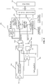
- FIG. 2 is a schematic structural diagram of a memory according to some embodiments of the present disclosure.
- the memory 200 includes: an input module 201, a memory array 202, a control module 203, and a selection module 204.
- the memory array 202 may include multiple memory blocks (Banks), such as Bank1, Bank2, ... to Bankn. Each Bank may include multiple memory units distributed in an array, and each memory unit has a row address and a column address. Therefore, each memory unit in the memory array 202 has a block (Bank) address, a row address, and a column address. When addressing the memory unit, firstly, the memory block where the memory unit is located is found according to the block address, and then the specific location of the memory unit in the memory block is found according to the row address and column address. Each memory block includes normal memory units and redundant memory units arranged in an array. The address decoding of the normal memory units and the address decoding of the redundant memory units require different decoding modes respectively.
- the input module 201 is configured to receive an address or command input signal including an address, a command, and a decoding selection instruction.
- the access address includes a block address, a row address, and a column address.
- the decoding selection instruction corresponds to the address decoding mode, and is used to instruct redundant decoding or normal decoding of the address.
- the control module 203 includes a plurality of memory block local control units, for example, memory block local control unit 1-memory block local control unit n, respectively, connected to the corresponding memory block Bank1 ⁇ memory block Bankn; the memory block local control units are configured to decode address or command input signals with corresponding block addresses to select the memory unit corresponding to the access address.
- memory block local control units for example, memory block local control unit 1-memory block local control unit n, respectively, connected to the corresponding memory block Bank1 ⁇ memory block Bankn; the memory block local control units are configured to decode address or command input signals with corresponding block addresses to select the memory unit corresponding to the access address.
- the input module 201 is connected to the control module 203.
- the address or command input signal received by the input module 201 after being processed, is input to the memory block local control unit corresponding to the block address in the control module 203 for decoding.
- the memory block local control unit includes: at least one decoding unit, configured to perform redundant decoding or normal decoding on the address or command input signal, the input of the decoding unit is coupled to the input module, and the output of the decoding unit is coupled to the memory block.
- each memory block local control unit includes two decoding units, a row decoding unit for row address decoding, and a column decoding unit for column address decoding.
- the input of the selection module 204 is coupled to the input module 201, and the output of the selection module 204 is coupled to the decoding unit in the memory block local control unit, and is configured to output, according to the address or command input signal, a first enable signal to the decoding unit in the corresponding memory block local control unit, to control the decoding unit to perform redundant decoding or normal decoding on the address or command input signal.
- FIG. 3 is a schematic structural diagram of the memory according to some embodiment of the present disclosure.
- FIG. 3 merely the circuit structure related to the column decoding part is shown.
- the input module 303 includes: an input interface, a buffer unit 3031 coupled to the input interface, and a logic control unit 3032 coupled to an output of the buffer unit 3031 and a normal address latch unit 3033 coupled to an output of the logic control unit 3032.
- the input interface includes 6 pins, which are pins CA0 ⁇ CA5, for inputting high and low electric signals to form a set of digital signals as the address or command input signal CA ⁇ 5:0>.
- a complete address or command input signal can be input through one input or multiple inputs.
- the address or command input signal includes information such as a block address, a column address, a row address, and a command.
- the command can be operation instructions such as decoding the row address or the column address, a reading operation and a writing operation, or refresh.
- the address or command input signal CA ⁇ 5:0> also includes a decoding selection instruction, the decoding selection instruction is configured to select redundant decoding or normal decoding on the address or command input signal.
- the pin when one of the pins of the input interface is not used as a valid address or command input pin at a certain clock edge, the pin is used to input the decoding selection command at the clock edge, thereby there is no need to add additional pins for the decoding selection instruction, and also there is no need to change the timing and path of the address or command input signal, thus realizing flexible and efficient decoding mode selection.
- the address or command input signal CA ⁇ 5:0> after passing through the buffer unit 3031 and being subjected to logic process by the logic control unit 3032, is sent to the normal address latch unit 3033 to latch the required column address signal ColAdrO ⁇ 9:4>, and later the column address signal ColAdrO ⁇ 9:4> is sent to the memory block local control unit 301 corresponding to the memory block address in the address or command input signal to perform column address decoding.
- the specific structure of the input module 303 may include technical variations known to those of ordinary skills in the art and will not be described in detail here.
- the memory block local control unit 301 includes a column decoding unit, and the memory block 302 is coupled to the output of the column secondary decoding unit 3013.
- the memory unit corresponding to the access address is selected according to the decoded access address output by the column secondary decoding unit 3013.
- the column decoding unit further includes a column normal pre-decoding unit 3011, a column redundant pre-decoding unit 3012, and a column secondary decoding unit 3013; and the outputs of the column redundant pre-decoding unit 3012 and the column normal pre-decoding unit 3011 are both coupled to the input of the column secondary decoding unit 3012.
- the address or command input signal is input to the column secondary decoding unit 3013 for secondary decoding to obtain the final column address information.
- the column address of the normal memory unit is obtained by decoding by the column normal pre-decoding unit 3011 and the column secondary decoding unit 3013, so that a column memory unit in the memory block 302 corresponding to the column address can be selected.
- the column address of the redundant memory unit is obtained, so that a column redundant memory unit in the memory block 302 corresponding to the column address can be selected.
- the memory block local control unit 301 further includes a first local latch unit 3015, the input of the first local latch unit 3015 is coupled to the output of the normal address latch unit 3033, the output of the first local latch unit 3015 is coupled to the inputs of the column redundant pre-decoding unit 3012 and the column normal pre-decoding unit 3011.
- the memory further includes a selection module 304, and the output of the selection module 304 is coupled to both the enable terminals of the column redundant pre-decoding unit 3012 and the enable end of the column normal pre-decoding unit 3011.
- the input of the selection module 304 is coupled to the input module 303 and is configured to receive the decoding selection instruction in the address or command input signal at the corresponding clock edge, and to control the column redundant pre-decoding unit 3012 to be enabled or control the column normal pre-decoding unit 3011 to be enabled according to the decoding selection instruction in the address or command input signal.
- the selection module 304 includes: a multiplexer MUX, the first input of the multiplexer MUX is coupled to the input module 303; the second input of the multiplexer MUX is connected to a reference level, in this embodiment, the reference level is low level 0.
- the control terminal of the selection module 304 is connected to a test control signal Cm0_ts_RedTest, and the test control signal, Cm0_ts_RedTest, is configured to control the multiplexer MUX to output a signal corresponding to the first input or the second input.
- the selection module 304 further includes a test enable latch unit 3041, and the input of the test enable latch unit 3041 is coupled to the output of the multiplexer MUX.
- the first enable signal RedColEnO output by the test enable latch unit 3041 is output to the memory block local control unit 301 for enabling the column normal pre-decoding unit 3011 or the column redundant pre-decoding unit 3012.
- the memory block local control unit 301 also includes a second local latch unit 3016.
- the input of the second local latch unit 3016 is coupled to the output of the selection module 304 for latching the first enable Signal RedColEnO; the output of the second local latch unit 3016 is coupled to the enable terminals of the column redundant pre-decoding unit 3012 and the column normal pre-decoding unit 3011.
- the normal address memory 3033 latches the required address information ColAdr ⁇ 9:4>; at the same time, the selection module 304 outputs the first enable signal RedColEnO based on the obtained decoding selection instruction in the address or command input signal.
- the column address signal ColAdr ⁇ 9:4> and the first enable signal RedColEnO reach the memory block local control unit 301 respectively, then are latched by the first local latch r unit 3015 and the second local latch unit 3016 respectively.
- the memory block local control unit 301 can be controlled to perform corresponding redundant decoding or normal decoding, thereby making the testing process more flexible. There is no need to switch the signal input interface.
- each latch unit is controlled by the same clock signal, CLK, so the control timings and the paths of the column address signal ColAdrO ⁇ 9:4> and the first enable signal RedColEn are completely consistent with each other, which can reduce human test errors, thereby improving the accuracy and convenience of the test.
- the local memory block control unit 3014 further includes a column address comparison unit 3014, the input of the column address comparison unit 3014 is coupled to the input module 303, and the output of the column address comparison unit 3014 is coupled to the enable terminals of the column normal pre-decoding unit 3011 and the column redundant pre-decoding unit 3011.
- the access address When the access address does not match the defective address, the access address is valid.
- the second enable signal RedColRepair 0, it enables (Enable) the column normal pre-decoding unit 3011, to perform column normal pre-decoding 3011 on the input signal to obtain the column address of the normal memory unit.
- FIG. 4 is a schematic structural diagram of a memory according to another embodiment of the present disclosure.
- FIG. 4 merely shows a schematic diagram of a circuit structure related to the column decoding.
- the input module 303 includes: an input interface, a buffer unit 3031 coupled to the input interface, a logic control unit 3032 coupled to the output of the buffer unit 3031, and a normal address latch unit 4033 coupled to the output of the logic control unit 3032.
- the address or command input signal CA ⁇ 5:0> after being buffered by the buffer unit 3031 and processed by the logic control unit 3032, is sent to the normal address latch unit 3033 to latch the desired row address signal RowAdr0 ⁇ 15:0>, and then the row address signal RowAdrO ⁇ 15:0> is sent to the row decoding unit in the local control unit 301 of the memory block corresponding to the block address in the address or command input signal to decode the row address.
- the row decoding unit in the memory block local control unit 301 includes: a row normal pre-decoding unit 4011, a row redundant pre-decoding unit 4012, and a row secondary decoding unit 4013.
- the outputs of row redundant pre-decoding unit 4012 and the the row normal pre-decoding unit 4011 are both coupled to the inputs of the row secondary decoding unit 4012, and the address or command input signal, after being subjected to row redundant decoding or row normal pre-decoding, is input to the row secondary decoding unit 4012 redundant decoding for secondary decoding, to obtain the final row address information.
- the memory block local control unit 301 further includes a first local latch unit 4015, which is configured to locally latch the row address signal RowAdrO ⁇ 15:0>.
- the input of the first local latch unit 4015 is coupled to the output of the normal address latch unit 3033, and the output of the first local latch unit 4015 is coupled to the inputs of the row redundant pre-decoding unit 4012 and the line normal pre-decoding unit 4011.
- the memory block local control unit 301 also includes a second local latch unit 4016.
- the input of the second local latch unit 4016 is coupled to the output of the selection module 304 and is configured to latch the first enable signal RedRowEn0.
- the output of the second local latch unit 4016 is coupled to the enable terminals of the row redundant pre-decoding unit 4012 and the row normal pre-decoding unit 4011.
- the local memory block control unit 301 further includes a row address comparison unit 4014; the input of the row address comparison unit 4014 is coupled to the input module 303, and the output of the row address comparison unit 4014 is coupled to the enable terminal of the row normal pre-decoding unit 4011 and the row redundant pre-decoding unit 4011.
- the row normal pre-decoding unit 4011 is enabled to perform row normal pre-decoding 4011 on the input signal to obtain the row address of the normal memory unit.
- the embodiment of the present disclosure also provides an addressing method for the memory.
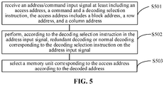
- FIG. 5 depicts the addressing method for a memory as the follows.
- Step S501 an address or command input signal is received, the address or command input signal includes at least an access address, a command, and a decoding selection instruction, where the access address includes a block address, a row address, and a column address.
- the address or command input signal may be received through a plurality of input pins.
- the address or command input signal includes a plurality of sets of digital signals, wherein each set of the digital signals includes a plurality of electrical level signals input through the plurality of input pins.
- the decoding selection instruction is a level signal input from an input pin in a set of digital signals, and the decoding selection instruction corresponds to a decoding mode of the address or command input signal.
- Step S502 redundant decoding or normal decoding is performed on the address or command input signal corresponding to the decoding selection instruction according to the decoding selection instruction in the address or command input signal.
- the redundant decoding includes redundant pre-decoding and secondary decoding
- the normal decoding includes normal pre-decoding and secondary decoding
- the corresponding decoding mode for the address or command input signal can be selected. For example, when the decoding selection instruction is 1, normal decoding is performed; when the decoding selection instruction is 0, redundant decoding is performed.
- Step S503 a memory unit corresponding to the access address is selected based on the decoded address.
- the addressing method for the memory of the present disclosure further includes: during normal use, comparing the access address in the address or command input signal with the defective address information, and performing relevant redundant decoding or normal decoding based on a result of the comparison. Specifically, when the access address matches the defective address, the access address is invalid, and redundant pre-decoding is performed on the input signal to obtain the address of the redundant memory unit that replaces the defective address. When the access address does not match the defective address, the access address is valid, and the input signal is normally decoded to obtain the address of the normal memory unit.
Landscapes
- Engineering & Computer Science (AREA)
- Microelectronics & Electronic Packaging (AREA)
- Computer Hardware Design (AREA)
- For Increasing The Reliability Of Semiconductor Memories (AREA)
Abstract
Description
- The present disclosure relates to the technical field of memory, and in particular to a memory and an addressing method therefor.
- In the design of Dynamic Random Access Memories (DRAMs), redundant cells are generally added internally to repair defective row storage locations and column storage locations at normal storage locations that occur during the manufacturing process.
-
FIG. 1 is a schematic diagram of the layout positions of normal and redundant storage units in an existing DRAM -
FIG. 1 merely shows word lines (WL) and bit lines (BL). Among them, 16 rows of redundant storage units are set for every 1,024 horizontal word lines (WLs), corresponding to 16 redundant word lines (RedWLs), and 16 columns of redundant storage units are set for every 512 vertical bit lines BLs, corresponding to 16 redundant bit lines (RedBLs). - In the memory chip testing phase, normal storage units need to be accessed to test whether each normal storage unit is valid. If a normal storage unit is invalid, the address of the invalid storage unit needs to be recorded, and a redundant storage unit is used instead of the invalid storage units for data storage.
- Therefore, in the chip test phase, it is necessary to test the normal storage units and the redundant storage units, respectively. Because the addresses of the normal storage units and the redundant storage units use different decoding modes, in the related art, the normal storage units and the redundant storage units are usually tested separately to access the corresponding address through different test paths and timing controls. During the test, it is necessary to switch frequently between the two tests. This switch increases the testing time. In addition, the difference in the test paths and the timing controls also easily introduces human test error, resulting in a decrease in test accuracy.
- Therefore, it is necessary to improve the memory addressing test efficiency in the related art.
- The disclosure provides a memory and an addressing method therefor to improve the test efficiency of the memory. The memory includes an input module for receiving an address or command input signal, wherein the address or command input signal includes an access address, a command, and a decoding selection instruction, wherein the access address includes a block address, a row address, and a column address; a memory array comprising a plurality of memory blocks, wherein each of the plurality of memory blocks includes a plurality of memory units arranged in an array;
- a control module, the control module comprises a plurality of memory block local control units, wherein each of the plurality of memory block local control units is connected to a respective one of the plurality of memory blocks, and is configured to decode the address or command input signal having a corresponding block address to select a memory unit corresponding to the access address wherein the plurality of memory block local control units each includes at least one decoding unit, wherein the decoding unit is configured to perform redundant decoding or normal decoding on the address or command input signal, wherein an input of the decoding unit is coupled to the input module, an output of the decoding unit is coupled to one of the plurality of memory units; and wherein the control module; and
- a selection module, wherein an input of the selection module is coupled to the input module, and an output of the selection module is coupled to the decoding unit, wherein the selection module is configured to output a first enable signal, to control the decoding unit to perform redundant decoding or normal decoding corresponding to the decoding selection instruction on the address or command input signal.
- In some examples, the decoding unit comprises: a redundant pre-decoding unit, a normal pre-decoding unit, and a secondary decoding unit; wherein the output of the selection module is coupled to an enable terminal of the redundant pre-decoding unit and an enable terminal of the normal pre-decoding unit; and wherein an output of the redundant pre-decoding unit and an output of the normal pre-decoding unit are both coupled to an input of the secondary decoding unit.
- In some examples, each of the plurality of the memory block local control units further comprises: an address comparison unit, wherein an input of the address comparison unit is coupled to the input module, and an output of the address comparison unit is coupled to the decoding unit, wherein the address comparison unit is configured to store defective address information, compare the access address in the address or command input signal with the defective address information, and output a second enable signal based on the comparison, and wherein the second enable signal is configured to control the decoding unit to perform redundant decoding or normal decoding on the address or command input signal.
- In some examples, the input module comprises: an input interface, a buffer unit coupled to the input interface, a logic control unit coupled to an output of the buffer unit, and a normal address latch unit coupled to an output of the logic control unit.
- In some examples, each of the plurality of memory block local control units further comprises: a first local latch unit, wherein an input of the first local latch unit is coupled to an output of the normal address latch unit of the input module.
- In some examples, the input module comprises: a plurality of input pins, wherein the address or command input signal comprises multiple sets of digital signals, wherein each set of the multiple sets of digital signals comprise a plurality of level signals input through a plurality of input pins, wherein the decoding selection instruction is a level signal, from one of the plurality of input pins, of one set of the multiple sets of digital signals, and the decoding selection instruction corresponds to a decoding mode for the address or command input signal.
- In some examples, the selection module comprises: a multiplexer comprising a first input of the multiplexer coupled to the input module, a second input coupled to a reference level, and a control terminal coupled to a test control signal, wherein the test control signal is configured to control the multiplexer to output a signal corresponding to the first input or the second input of the multiplexer.
- In some examples, the selection module further comprises: a test enable latch unit; an input of the test enable latch unit is coupled to an output of the multiplexer.
- In some examples, the decoding unit further comprises: a second local latch unit, wherein an input of the second local latch unit is coupled to an output of the test enable latch unit of the selection module.
- In some examples, each of the plurality of memory block local control units comprises: two decoding units, wherein the two decoding units decode the row address and the column address, respectively, in the access address.
- The present disclosure also provides an addressing method for a memory, comprising: receiving an address or command input signal at least comprising: an access address, a command, and a decoding selection instruction, where the access address includes a block address, a row address, and a column address; performing redundant decoding or normal decoding on the address or command input signal according to the decoding selection instruction in the address or command input signal; and selecting a memory unit corresponding to the decoded access address.
- In some examples, the redundant decoding comprises redundant pre-decoding and secondary decoding; and wherein the normal decoding includes normal pre-decoding and secondary decoding.
- In some examples, the method comprises: comparing the access address in the address or command input signal with a defective address information in normal use of the memory, and performing redundant decoding or normal decoding on the address or command input signal according to a result of the comparison.
- In some examples, the address or command input signal is received through a plurality of input pins, wherein the address or command input signal comprises a plurality of sets of digital signals, wherein each of the plurality of sets of digital signals include a plurality of level signals input through the plurality of input pins, and wherein the decoding selection instruction is one of the plurality of level signals, from one of the plurality of input pins, of one of the plurality of sets of digital signals, and wherein the decoding selection instruction corresponds to a decoding mode for the address or command input signal.
- In some examples, the addressing method for the memory further comprises: decoding the row address and the column address separately in the address or command input signal.
- The memory of the present disclosure can control address or command input signal to perform the corresponding redundant decoding or normal decoding, by setting the decoding selection instruction, the test process is made more flexible without having to switch the signal input interface. The path and timing of the address signal input are consistent with the generating path and timing of the first enable signal. As a result, human test errors can be reduced, thereby improving the test accuracy and convenience.
-
-
FIG. 1 is a schematic structural diagram of an existing memory array; -
FIG. 2 is a schematic structural diagram of a memory according to some embodiments of the present disclosure; -
FIG. 3 is a schematic structural diagram of a memory according to some embodiments of the present disclosure; -
FIG. 4 is a schematic structural diagram of a memory according to some embodiments of the present disclosure; and -
Fig. 5 is a memory addressing method according to some embodiments of the present disclosure. - The specific implementation of a memory and its addressing method therefor according to the embodiments of the present disclosure will be described in detail with reference to the accompanying drawings in the following paragraphs.
-
FIG. 2 is a schematic structural diagram of a memory according to some embodiments of the present disclosure. - The
memory 200 includes: aninput module 201, amemory array 202, acontrol module 203, and aselection module 204. - The
memory array 202 may include multiple memory blocks (Banks), such as Bank1, Bank2, ... to Bankn. Each Bank may include multiple memory units distributed in an array, and each memory unit has a row address and a column address. Therefore, each memory unit in thememory array 202 has a block (Bank) address, a row address, and a column address. When addressing the memory unit, firstly, the memory block where the memory unit is located is found according to the block address, and then the specific location of the memory unit in the memory block is found according to the row address and column address. Each memory block includes normal memory units and redundant memory units arranged in an array. The address decoding of the normal memory units and the address decoding of the redundant memory units require different decoding modes respectively. - The
input module 201 is configured to receive an address or command input signal including an address, a command, and a decoding selection instruction. The access address includes a block address, a row address, and a column address. The decoding selection instruction corresponds to the address decoding mode, and is used to instruct redundant decoding or normal decoding of the address. - The
control module 203 includes a plurality of memory block local control units, for example, memory block local control unit 1-memory block local control unit n, respectively, connected to the corresponding memory block Bank1∼memory block Bankn; the memory block local control units are configured to decode address or command input signals with corresponding block addresses to select the memory unit corresponding to the access address. - The
input module 201 is connected to thecontrol module 203. The address or command input signal received by theinput module 201, after being processed, is input to the memory block local control unit corresponding to the block address in thecontrol module 203 for decoding. The memory block local control unit includes: at least one decoding unit, configured to perform redundant decoding or normal decoding on the address or command input signal, the input of the decoding unit is coupled to the input module, and the output of the decoding unit is coupled to the memory block. Generally, each memory block local control unit includes two decoding units, a row decoding unit for row address decoding, and a column decoding unit for column address decoding. - The input of the
selection module 204 is coupled to theinput module 201, and the output of theselection module 204 is coupled to the decoding unit in the memory block local control unit, and is configured to output, according to the address or command input signal, a first enable signal to the decoding unit in the corresponding memory block local control unit, to control the decoding unit to perform redundant decoding or normal decoding on the address or command input signal. -
FIG. 3 is a schematic structural diagram of the memory according to some embodiment of the present disclosure. - In
FIG. 3 , merely the circuit structure related to the column decoding part is shown. - The
input module 303 includes: an input interface, abuffer unit 3031 coupled to the input interface, and alogic control unit 3032 coupled to an output of thebuffer unit 3031 and a normaladdress latch unit 3033 coupled to an output of thelogic control unit 3032. - In this specific implementation, taking LPDDR4 as an example, the input interface includes 6 pins, which are pins CA0∼CA5, for inputting high and low electric signals to form a set of digital signals as the address or command input signal CA<5:0>. A complete address or command input signal can be input through one input or multiple inputs. The address or command input signal includes information such as a block address, a column address, a row address, and a command. The command can be operation instructions such as decoding the row address or the column address, a reading operation and a writing operation, or refresh. The address or command input signal CA<5:0> also includes a decoding selection instruction, the decoding selection instruction is configured to select redundant decoding or normal decoding on the address or command input signal.
- It is usually necessary to transmit multiple sets of digital signals at multiple clock edges to achieve the transmission of the complete commands and address information, thus forming a complete address or command input signal. Among the address or command input signal input at a specific clock edge, there is an input signal from a pin that is useless for address and command information, for example, the input pin CA3 of LPDDR4 is not used as a command or address input at a certain clock edge. Therefore, according to the embodiment of the present disclosure, a decoding selection command can be sent to the specific clock edge, and the decoding selection command received by pin CA3 at the specific clock edge is only used as a selection command for the subsequent decoding mode, and will not impact the final address decoding result.
- In the specific embodiment of the present disclosure, when one of the pins of the input interface is not used as a valid address or command input pin at a certain clock edge, the pin is used to input the decoding selection command at the clock edge, thereby there is no need to add additional pins for the decoding selection instruction, and also there is no need to change the timing and path of the address or command input signal, thus realizing flexible and efficient decoding mode selection.
- According to the embodiment, the address or command input signal CA<5:0>, after passing through the
buffer unit 3031 and being subjected to logic process by thelogic control unit 3032, is sent to the normaladdress latch unit 3033 to latch the required column address signal ColAdrO<9:4>, and later the column address signal ColAdrO<9:4> is sent to the memory blocklocal control unit 301 corresponding to the memory block address in the address or command input signal to perform column address decoding. - In another embodiment according to the present disclosure, the specific structure of the
input module 303 may include technical variations known to those of ordinary skills in the art and will not be described in detail here. - In the above embodiment, the memory block
local control unit 301 includes a column decoding unit, and thememory block 302 is coupled to the output of the columnsecondary decoding unit 3013. The memory unit corresponding to the access address is selected according to the decoded access address output by the columnsecondary decoding unit 3013. - The column decoding unit further includes a column
normal pre-decoding unit 3011, a columnredundant pre-decoding unit 3012, and a columnsecondary decoding unit 3013; and the outputs of the columnredundant pre-decoding unit 3012 and the columnnormal pre-decoding unit 3011 are both coupled to the input of the columnsecondary decoding unit 3012. After column redundant decoding or column normal pre-decoding, the address or command input signal is input to the columnsecondary decoding unit 3013 for secondary decoding to obtain the final column address information. For example, the column address of the normal memory unit is obtained by decoding by the columnnormal pre-decoding unit 3011 and the columnsecondary decoding unit 3013, so that a column memory unit in thememory block 302 corresponding to the column address can be selected. For another example, after decoding by the columnredundant pre-decoding unit 3012 and the columnsecondary decoding unit 3013, the column address of the redundant memory unit is obtained, so that a column redundant memory unit in thememory block 302 corresponding to the column address can be selected. - According to the embodiment, the memory block
local control unit 301 further includes a firstlocal latch unit 3015, the input of the firstlocal latch unit 3015 is coupled to the output of the normaladdress latch unit 3033, the output of the firstlocal latch unit 3015 is coupled to the inputs of the columnredundant pre-decoding unit 3012 and the columnnormal pre-decoding unit 3011. - After the column address signal ColAdrO<9:4> output from the normal
address latch unit 3033 passes through the firstlocal latch unit 3015, it is output to the columnredundant pre-decoding unit 3012 and the columnnormal pre-decoding unit 3011. - The memory further includes a
selection module 304, and the output of theselection module 304 is coupled to both the enable terminals of the columnredundant pre-decoding unit 3012 and the enable end of the columnnormal pre-decoding unit 3011. The input of theselection module 304 is coupled to theinput module 303 and is configured to receive the decoding selection instruction in the address or command input signal at the corresponding clock edge, and to control the columnredundant pre-decoding unit 3012 to be enabled or control the columnnormal pre-decoding unit 3011 to be enabled according to the decoding selection instruction in the address or command input signal.. For example, if the decode selection instruction is 1 (high level), theselection module 304 outputs the first enable signal RedColEn=1, which controls the columnredundant pre-decoding unit 3012 to be enabled, to perform column redundant decoding on the address or command input signal ColAdrO<9:4>, in order to obtain the column address of the redundant memory unit. If the decoding selection instruction is 0 (low level), theselection module 304 outputs the first enable signal RedColEn=0, which controls the columnnormal pre-decoding unit 3011 to be enabled to perform column normal decoding on the address or command input signal ColAdrO<9:4>, in order to obtain the column address of the normal memory unit. - According to the embodiment, the
selection module 304 includes: a multiplexer MUX, the first input of the multiplexer MUX is coupled to theinput module 303; the second input of the multiplexer MUX is connected to a reference level, in this embodiment, the reference level islow level 0. The control terminal of theselection module 304 is connected to a test control signal Cm0_ts_RedTest, and the test control signal, Cm0_ts_RedTest, is configured to control the multiplexer MUX to output a signal corresponding to the first input or the second input. Theselection module 304 further includes a test enablelatch unit 3041, and the input of the test enablelatch unit 3041 is coupled to the output of the multiplexer MUX. - When the test control signal, Cm0_ts_RedTest=1, the multiplexer MUX outputs the decoding selection instruction input by the first input to the test enable
latch unit 3041. The first enable signal RedColEnO output by the test enablelatch unit 3041 is output to the memory blocklocal control unit 301 for enabling the columnnormal pre-decoding unit 3011 or the columnredundant pre-decoding unit 3012. - The memory block
local control unit 301 also includes a secondlocal latch unit 3016. The input of the secondlocal latch unit 3016 is coupled to the output of theselection module 304 for latching the first enable Signal RedColEnO; the output of the secondlocal latch unit 3016 is coupled to the enable terminals of the columnredundant pre-decoding unit 3012 and the columnnormal pre-decoding unit 3011. - After the address or command input signal input through the
input module 303 passes through thebuffer unit 3031 and thelogic control unit 3032, thenormal address memory 3033 latches the required address information ColAdr<9:4>; at the same time, theselection module 304 outputs the first enable signal RedColEnO based on the obtained decoding selection instruction in the address or command input signal. The column address signal ColAdr<9:4> and the first enable signal RedColEnO reach the memory blocklocal control unit 301 respectively, then are latched by the first locallatch r unit 3015 and the secondlocal latch unit 3016 respectively. When the secondlocal latch unit 3016 outputs the first enable signal RedColEn=1, the decoding of the normal path is stopped, and the columnredundant pre-decoding unit 3012 is enabled; when the first enable signal RedColEn=0,the columnredundant pre-decoding unit 3012 is stopped, and the normal decoding path will not be affected. In a specific implementation, when the decode selection instruction is 1, the first enable signal RedColEn=1; and when the decode selection instruction is 0, the first enable signal RedColEn=0. - When performing column test on redundant memory units and normal memory units, by setting the decoding selection instruction, the memory block
local control unit 301 can be controlled to perform corresponding redundant decoding or normal decoding, thereby making the testing process more flexible. There is no need to switch the signal input interface. - When switching between the normal memory unit and the redundant memory unit test, only the decoding selection instruction needs to be controlled. Each latch unit is controlled by the same clock signal, CLK, so the control timings and the paths of the column address signal ColAdrO<9:4> and the first enable signal RedColEn are completely consistent with each other, which can reduce human test errors, thereby improving the accuracy and convenience of the test.
- According to the embodiment, the local memory
block control unit 3014 further includes a columnaddress comparison unit 3014, the input of the columnaddress comparison unit 3014 is coupled to theinput module 303, and the output of the columnaddress comparison unit 3014 is coupled to the enable terminals of the columnnormal pre-decoding unit 3011 and the columnredundant pre-decoding unit 3011. - The
address comparison unit 3014 is configured to store the defective address information acquired during the test. When performing normal reading and writing operations on the memory, theaddress comparison unit 3014 compares the column address signal ColAdr<9:4> with the defective address information; outputs a second enable signal RedColRepair based on a result of the comparison, in order to control the decoding unit to perform corresponding redundant decoding or normal decoding on the address or command input signal. Specifically, when the access address matches the defective address, the second enable signal RedColRepair=1, the access address is invalid, so as to enable the columnredundant pre-decoding unit 3012 to perform column redundant pre-decoding on the input signal, to obtain the column address of the redundant memory unit that replaces the defective address. When the access address does not match the defective address, the access address is valid. When the second enable signal RedColRepair=0, it enables (Enable) the columnnormal pre-decoding unit 3011, to perform columnnormal pre-decoding 3011 on the input signal to obtain the column address of the normal memory unit. - When performing normal reading and writing operations on the memory, the test control signal, Cm0_ts_RedTest=0, can be set so that the
selection module 304 would not obtain the decoding selection instruction, therefore stopping the selection function of theselection module 304 for the redundant decoding path. - Please refer to
FIG. 4 , which is a schematic structural diagram of a memory according to another embodiment of the present disclosure. -
FIG. 4 merely shows a schematic diagram of a circuit structure related to the column decoding. - The
input module 303 includes: an input interface, abuffer unit 3031 coupled to the input interface, alogic control unit 3032 coupled to the output of thebuffer unit 3031, and a normal address latch unit 4033 coupled to the output of thelogic control unit 3032. The address or command input signal CA<5:0> , after being buffered by thebuffer unit 3031 and processed by thelogic control unit 3032, is sent to the normaladdress latch unit 3033 to latch the desired row address signal RowAdr0 <15:0>, and then the row address signal RowAdrO<15:0> is sent to the row decoding unit in thelocal control unit 301 of the memory block corresponding to the block address in the address or command input signal to decode the row address. - The row decoding unit in the memory block
local control unit 301 includes: a rownormal pre-decoding unit 4011, a rowredundant pre-decoding unit 4012, and a rowsecondary decoding unit 4013. The outputs of rowredundant pre-decoding unit 4012 and the the rownormal pre-decoding unit 4011 are both coupled to the inputs of the rowsecondary decoding unit 4012, and the address or command input signal, after being subjected to row redundant decoding or row normal pre-decoding, is input to the rowsecondary decoding unit 4012 redundant decoding for secondary decoding, to obtain the final row address information. - According to the embodiment, the memory block
local control unit 301 further includes a firstlocal latch unit 4015, which is configured to locally latch the row address signal RowAdrO<15:0>. The input of the firstlocal latch unit 4015 is coupled to the output of the normaladdress latch unit 3033, and the output of the firstlocal latch unit 4015 is coupled to the inputs of the rowredundant pre-decoding unit 4012 and the linenormal pre-decoding unit 4011. - The memory block
local control unit 301 also includes a secondlocal latch unit 4016. The input of the secondlocal latch unit 4016 is coupled to the output of theselection module 304 and is configured to latch the first enable signal RedRowEn0. The output of the secondlocal latch unit 4016 is coupled to the enable terminals of the rowredundant pre-decoding unit 4012 and the rownormal pre-decoding unit 4011. - When the test control signal Cm0_ts_RedTest=1, the multiplexer MUX outputs the decoding selection instruction input from the first input to the test enable
latch unit 3041; after passing the test enablelatch unit 3041, the first enable signal RedRowEn0 is output to the memory blocklocal control unit 301 for enabling the rownormal pre-decoding unit 4011 or the rowredundant pre-decoding unit 4012. When the locally latched first enable signal RedRowEn=1, the decoding of the normal path is stopped, and the rowredundant pre-decoding unit 4012 is enabled; when the first enable signal RedRowEn=0, then the rowredundant pre-decoding unit 4012 is stopped, and the normal decoding path will not be affected. - Corresponding to the column test, when performing the row test, one can control whether to perform redundant decoding or normal decoding on the row address signal through the decoding selection instruction in the address or command input signal.
- In this specific embodiment, the local memory
block control unit 301 further includes a rowaddress comparison unit 4014; the input of the rowaddress comparison unit 4014 is coupled to theinput module 303, and the output of the rowaddress comparison unit 4014 is coupled to the enable terminal of the rownormal pre-decoding unit 4011 and the rowredundant pre-decoding unit 4011. - The row
address comparison unit 4014 is configured to store the defective address information acquired during the test. When performing normal reading and writing operations on the memory, the rowaddress comparison unit 4014 compares the row address signal RowAdr<15:0> with the defective address information, and outputs a second enable signal RedRowRepair according to a result of the comparison, to control the decoding unit to perform corresponding redundant decoding or normal decoding on the address or command input signal. Specifically, when the access address matches the defective address, the second enable signal RedRowRepair=1, the access address is invalid, so as to enable the row redundant pre-decoding unit 4012to perform redundant pre-decoding on the input signal. to obtain the row address of the redundant memory unit that replaces the defective address; when the access address does not match the defective address, the access address is valid. When the second enable signal RedRowRepair=0, the rownormal pre-decoding unit 4011 is enabled to perform rownormal pre-decoding 4011 on the input signal to obtain the row address of the normal memory unit. - When performing normal reading and writing operations on the memory, the test control signal Cm0_ts_RedTest=0 can be set so that the
selection module 304 does not obtain the decoding selection instruction, and the selection function of theselection module 304 for the redundant decoding path is stopped. At this time, it is possible that the decoding selection instruction is not set. - The embodiment of the present disclosure also provides an addressing method for the memory.
-
FIG. 5 depicts the addressing method for a memory as the follows. - In Step S501, an address or command input signal is received, the address or command input signal includes at least an access address, a command, and a decoding selection instruction, where the access address includes a block address, a row address, and a column address.
- The address or command input signal may be received through a plurality of input pins. The address or command input signal includes a plurality of sets of digital signals, wherein each set of the digital signals includes a plurality of electrical level signals input through the plurality of input pins. The decoding selection instruction is a level signal input from an input pin in a set of digital signals, and the decoding selection instruction corresponds to a decoding mode of the address or command input signal.
- In Step S502, redundant decoding or normal decoding is performed on the address or command input signal corresponding to the decoding selection instruction according to the decoding selection instruction in the address or command input signal.
- Here, the redundant decoding includes redundant pre-decoding and secondary decoding, and the normal decoding includes normal pre-decoding and secondary decoding.
- By setting the decoding selection instruction, the corresponding decoding mode for the address or command input signal can be selected. For example, when the decoding selection instruction is 1, normal decoding is performed; when the decoding selection instruction is 0, redundant decoding is performed.
- In Step S503, a memory unit corresponding to the access address is selected based on the decoded address.
- The above steps can be applied to decode the row address and column address, respectively.
- By setting the corresponding decoding selection instruction, one can switch the access to the redundant memory unit and the normal memory unit, making it more flexible in the testing process, meanwhile the control timing is consistent, avoiding human test errors and improving the test accuracy and flexibility.
- The addressing method for the memory of the present disclosure further includes: during normal use, comparing the access address in the address or command input signal with the defective address information, and performing relevant redundant decoding or normal decoding based on a result of the comparison. Specifically, when the access address matches the defective address, the access address is invalid, and redundant pre-decoding is performed on the input signal to obtain the address of the redundant memory unit that replaces the defective address. When the access address does not match the defective address, the access address is valid, and the input signal is normally decoded to obtain the address of the normal memory unit.
- The above are only the preferred embodiments of the present disclosure. It should be pointed out that for those of ordinary skill in the art, without departing from the principle of the present disclosure, several improvements and modifications can be made, and these improvements and modifications should also be considered in the protection scope of the invention.
Claims (15)
- A memory, comprising:an input module for receiving an address or command input signal, wherein the address or command input signal includes an access address, a command, and a decoding selection instruction, wherein the access address includes a block address, a row address, and a column address;a memory array comprising a plurality of memory blocks, wherein each of the plurality of memory blocks includes a plurality of memory units arranged in an array;a control module, wherein the control module comprises a plurality of memory block local control units, wherein each of the plurality of memory block local control units is connected to a respective one of the plurality of memory blocks, and is configured to decode the address or command input signal having a corresponding block address to select a memory unit corresponding to the access address wherein the plurality of memory block local control units each includes at least one decoding unit, wherein the decoding unit is configured to perform redundant decoding or normal decoding on the address or command input signal, wherein an input of the decoding unit is coupled to the input module, an output of the decoding unit is coupled to one of the plurality of memory units; and wherein the control module; anda selection module, wherein an input of the selection module is coupled to the input module, and an output of the selection module is coupled to the decoding unit, wherein the selection module is configured to output a first enable signal, to control the decoding unit to perform redundant decoding or normal decoding corresponding to the decoding selection instruction on the address or command input signal.
- The memory according to claim 1, wherein the decoding unit comprises a redundant pre-decoding unit, a normal pre-decoding unit, and a secondary decoding unit; wherein the output of the selection module is coupled to an enable terminal of the redundant pre-decoding unit and an enable terminal of the normal pre-decoding unit; and wherein an output of the redundant pre-decoding unit and an output of the normal pre-decoding unit are both coupled to an input of the secondary decoding unit.
- The memory according to claim 1, wherein each of the plurality of the memory block local control units further comprises an address comparison unit, wherein an input of the address comparison unit is coupled to the input module, and an output of the address comparison unit is coupled to the decoding unit, wherein the address comparison unit is configured to store defective address information, compare the access address in the address or command input signal with the defective address information, and output a second enable signal based on the comparison, and wherein the second enable signal is configured to control the decoding unit to perform redundant decoding or normal decoding on the address or command input signal.
- The memory according to claim 1, wherein the input module comprises: an input interface, a buffer unit coupled to the input interface, a logic control unit coupled to an output of the buffer unit, and a normal address latch unit coupled to an output of the logic control unit.
- The memory according to claim 4, wherein each of the plurality of memory block local control units further comprises a first local latch unit, wherein an input of the first local latch unit is coupled to an output of the normal address latch unit of the input module.
- The memory of claim 1, wherein the input module comprises a plurality of input pins, wherein the address or command input signal comprises multiple sets of digital signals, wherein each set of the multiple sets of digital signals comprise a plurality of level signals input through a plurality of input pins, wherein the decoding selection instruction is a level signal, from one of the plurality of input pins, of one set of the multiple sets of digital signals, and the decoding selection instruction corresponds to a decoding mode for the address or command input signal.
- The memory according to claim 1, wherein the selection module comprises: a multiplexer comprising a first input of the multiplexer coupled to the input module, a second input coupled to a reference level, and a control terminal coupled to a test control signal, wherein the test control signal is configured to control the multiplexer to output a signal corresponding to the first input or the second input of the multiplexer.
- The memory according to claim 7, wherein the selection module further comprises: a test enable latch unit, wherein an input of the test enable latch unit is coupled to an output of the multiplexer.
- The memory according to claim 8, wherein the decoding unit further comprises: a second local latch unit, wherein an input of the second local latch unit is coupled to an output of the test enable latch unit of the selection module.
- The memory according to claim 1, wherein each of the plurality of memory block local control units comprises two decoding units, wherein the two decoding units are configured to decode the row address and the column address, respectively, in the access address.
- An addressing method for a memory, comprising:receiving an address or command input signal at least comprising: an access address, a command, and a decoding selection instruction, where the access address includes a block address, a row address, and a column address;performing redundant decoding or normal decoding on the address or command input signal according to the decoding selection instruction in the address or command input signal; andselecting a memory unit corresponding to the decoded access address.
- The addressing method for the memory according to claim 11, wherein the redundant decoding comprises redundant pre-decoding and secondary decoding; and wherein the normal decoding includes normal pre-decoding and secondary decoding.
- The addressing method for the memory according to claim 11, further comprising:
comparing the access address in the address or command input signal with a defective address information in normal use of the memory, and performing redundant decoding or normal decoding on the address or command input signal according to a result of the comparison. - The addressing method for the memory according to claim 11, wherein the address or command input signal is received through a plurality of input pins, wherein the address or command input signal comprises a plurality of sets of digital signals, wherein each of the plurality of sets of digital signals include a plurality of level signals input through the plurality of input pins, and wherein the decoding selection instruction is one of the plurality of level signals, from one of the plurality of input pins, of one of the plurality of sets of digital signals, and wherein the decoding selection instruction corresponds to a decoding mode for the address or command input signal.
- The addressing method for the memory according to any one of claims 11 to 14, further comprising decoding the row address and the column address separately in the address or command input signal.
Applications Claiming Priority (2)
| Application Number | Priority Date | Filing Date | Title |
|---|---|---|---|
| CN201910904486.4A CN112634960B (en) | 2019-09-24 | 2019-09-24 | Memory and its addressing method |
| PCT/CN2019/121162 WO2021056804A1 (en) | 2019-09-24 | 2019-11-27 | Memory and addressing method therefor |
Publications (3)
| Publication Number | Publication Date |
|---|---|
| EP3896693A1 true EP3896693A1 (en) | 2021-10-20 |
| EP3896693A4 EP3896693A4 (en) | 2022-04-06 |
| EP3896693B1 EP3896693B1 (en) | 2023-10-25 |
Family
ID=75164815
Family Applications (1)
| Application Number | Title | Priority Date | Filing Date |
|---|---|---|---|
| EP19947164.0A Active EP3896693B1 (en) | 2019-09-24 | 2019-11-27 | Memory and addressing method therefor |
Country Status (4)
| Country | Link |
|---|---|
| US (1) | US11423999B2 (en) |
| EP (1) | EP3896693B1 (en) |
| CN (1) | CN112634960B (en) |
| WO (1) | WO2021056804A1 (en) |
Families Citing this family (5)
| Publication number | Priority date | Publication date | Assignee | Title |
|---|---|---|---|---|
| CN112634960B (en) | 2019-09-24 | 2024-10-15 | 长鑫存储技术有限公司 | Memory and its addressing method |
| CN112583259B (en) | 2019-09-27 | 2022-03-18 | 长鑫存储技术有限公司 | Power module and memory |
| CN116486862B (en) | 2022-01-13 | 2024-07-26 | 长鑫存储技术有限公司 | Address decoding circuit, memory and control method |
| US12537048B2 (en) * | 2022-08-22 | 2026-01-27 | Micron Technology, Inc. | Semiconductor device having memory cell array divided into plural memory mats |
| CN120390959A (en) * | 2023-11-28 | 2025-07-29 | 长江存储科技有限责任公司 | Memory device, system and decoding circuit |
Family Cites Families (17)
| Publication number | Priority date | Publication date | Assignee | Title |
|---|---|---|---|---|
| KR950013342B1 (en) * | 1992-10-06 | 1995-11-02 | 삼성전자주식회사 | Fault Relief Circuit in Semiconductor Memory Device |
| US5519657A (en) * | 1993-09-30 | 1996-05-21 | Mitsubishi Denki Kabushiki Kaisha | Semiconductor memory device having a redundant memory array and a testing method thereof |
| JPH07226100A (en) * | 1994-02-15 | 1995-08-22 | Nec Corp | Semiconductor memory |
| KR0170271B1 (en) * | 1995-12-30 | 1999-03-30 | 김광호 | Semiconductor memory apparatus having redundant cell test control circuit |
| KR100256819B1 (en) * | 1997-06-30 | 2000-05-15 | 김영환 | Synchronous DRAM stabilizes redundant operation |
| US6195762B1 (en) * | 1998-06-24 | 2001-02-27 | Micron Techonology, Inc. | Circuit and method for masking a dormant memory cell |
| US6208570B1 (en) * | 1998-08-13 | 2001-03-27 | Texas Instruments Incorporated | Redundancy test method for a semiconductor memory |
| KR100319893B1 (en) * | 1999-07-01 | 2002-01-10 | 윤종용 | Semiconductor memory device capable of easily distinguishing location of defective memory cell by testing selectively block redundancy memory cell block |
| JP2001243795A (en) * | 1999-12-24 | 2001-09-07 | Nec Corp | Semiconductor memory |
| JP2001184890A (en) * | 1999-12-27 | 2001-07-06 | Mitsubishi Electric Corp | Semiconductor storage device |
| US6587804B1 (en) * | 2000-08-14 | 2003-07-01 | Micron Technology, Inc. | Method and apparatus providing improved data path calibration for memory devices |
| JP2005267817A (en) * | 2004-03-22 | 2005-09-29 | Oki Electric Ind Co Ltd | Semiconductor memory device and method of reading redundancy saving address |
| KR20160043711A (en) * | 2014-10-14 | 2016-04-22 | 에스케이하이닉스 주식회사 | Repair circuit and semiconductor memory device including the same |
| KR20160056586A (en) * | 2014-11-12 | 2016-05-20 | 에스케이하이닉스 주식회사 | Repair circuit and semiconductor memory device including the same |
| KR102389722B1 (en) * | 2017-11-29 | 2022-04-25 | 에스케이하이닉스 주식회사 | Semiconductor Memory Apparatus |
| CN210606641U (en) * | 2019-09-24 | 2020-05-22 | 长鑫存储技术有限公司 | memory |
| CN112634960B (en) | 2019-09-24 | 2024-10-15 | 长鑫存储技术有限公司 | Memory and its addressing method |
-
2019
- 2019-09-24 CN CN201910904486.4A patent/CN112634960B/en active Active
- 2019-11-27 EP EP19947164.0A patent/EP3896693B1/en active Active
- 2019-11-27 WO PCT/CN2019/121162 patent/WO2021056804A1/en not_active Ceased
- 2019-11-27 US US17/257,532 patent/US11423999B2/en active Active
Also Published As
| Publication number | Publication date |
|---|---|
| CN112634960A (en) | 2021-04-09 |
| US11423999B2 (en) | 2022-08-23 |
| EP3896693A4 (en) | 2022-04-06 |
| US20220270700A9 (en) | 2022-08-25 |
| EP3896693B1 (en) | 2023-10-25 |
| WO2021056804A1 (en) | 2021-04-01 |
| US20220028471A1 (en) | 2022-01-27 |
| CN112634960B (en) | 2024-10-15 |
Similar Documents
| Publication | Publication Date | Title |
|---|---|---|
| EP3896693B1 (en) | Memory and addressing method therefor | |
| US6252800B1 (en) | Semiconductor memory device | |
| US11972828B2 (en) | Repair circuit, memory, and repair method | |
| US20180019024A1 (en) | Semiconductor memory device for performing a post package repair operation and operating method thereof | |
| US6469949B1 (en) | Fuse latch array system for an embedded DRAM having a micro-cell architecture | |
| US20140126301A1 (en) | Memory device and test method thereof | |
| US10325669B2 (en) | Error information storage circuit and semiconductor apparatus including the same | |
| US7605434B2 (en) | Semiconductor memory device to which test data is written | |
| US10032523B2 (en) | Memory device including extra capacity and stacked memory device including the same | |
| US7266036B2 (en) | Semiconductor memory device | |
| US8270237B2 (en) | Semiconductor device, relief-address-information writing device, and relief-address-information writing method | |
| US20220262448A1 (en) | Memory device and memory system for executing a test | |
| JP2006268971A (en) | Semiconductor memory device and its test method | |
| US6684355B2 (en) | Memory testing apparatus and method | |
| KR100336955B1 (en) | Semiconductor storage device | |
| CN210606641U (en) | memory | |
| US10643731B2 (en) | Semiconductor memory apparatus | |
| JP4939870B2 (en) | Semiconductor memory device and test method thereof | |
| US20080244157A1 (en) | Semiconductor memory device | |
| US6928594B2 (en) | Semiconductor integrated circuit | |
| US20110228620A1 (en) | Testing method for semiconductor memory device | |
| CN115620772A (en) | Method for accessing word line and structure of word line decoding circuit | |
| US6628562B2 (en) | Method and apparatus for high-speed read operation in semiconductor memory | |
| US6407954B2 (en) | Nonvolatile semiconductor memory device | |
| US12555616B2 (en) | Memory device for outputting data and method of operating the same |
Legal Events
| Date | Code | Title | Description |
|---|---|---|---|
| STAA | Information on the status of an ep patent application or granted ep patent |
Free format text: STATUS: THE INTERNATIONAL PUBLICATION HAS BEEN MADE |
|
| PUAI | Public reference made under article 153(3) epc to a published international application that has entered the european phase |
Free format text: ORIGINAL CODE: 0009012 |
|
| STAA | Information on the status of an ep patent application or granted ep patent |
Free format text: STATUS: REQUEST FOR EXAMINATION WAS MADE |
|
| 17P | Request for examination filed |
Effective date: 20210712 |
|
| AK | Designated contracting states |
Kind code of ref document: A1 Designated state(s): AL AT BE BG CH CY CZ DE DK EE ES FI FR GB GR HR HU IE IS IT LI LT LU LV MC MK MT NL NO PL PT RO RS SE SI SK SM TR |
|
| REG | Reference to a national code |
Ref country code: DE Ref legal event code: R079 Free format text: PREVIOUS MAIN CLASS: G11C0011406300 Ipc: G11C0029240000 Ref country code: DE Ref legal event code: R079 Ref document number: 602019040375 Country of ref document: DE Free format text: PREVIOUS MAIN CLASS: G11C0011406300 Ipc: G11C0029240000 |
|
| A4 | Supplementary search report drawn up and despatched |
Effective date: 20220303 |
|
| RIC1 | Information provided on ipc code assigned before grant |
Ipc: G11C 29/00 20060101ALI20220225BHEP Ipc: G11C 8/06 20060101ALI20220225BHEP Ipc: G11C 11/4063 20060101ALI20220225BHEP Ipc: G11C 11/408 20060101ALI20220225BHEP Ipc: G11C 29/24 20060101AFI20220225BHEP |
|
| STAA | Information on the status of an ep patent application or granted ep patent |
Free format text: STATUS: EXAMINATION IS IN PROGRESS |
|
| 17Q | First examination report despatched |
Effective date: 20221129 |
|
| DAV | Request for validation of the european patent (deleted) | ||
| DAX | Request for extension of the european patent (deleted) | ||
| GRAP | Despatch of communication of intention to grant a patent |
Free format text: ORIGINAL CODE: EPIDOSNIGR1 |
|
| STAA | Information on the status of an ep patent application or granted ep patent |
Free format text: STATUS: GRANT OF PATENT IS INTENDED |
|
| INTG | Intention to grant announced |
Effective date: 20230515 |
|
| GRAS | Grant fee paid |
Free format text: ORIGINAL CODE: EPIDOSNIGR3 |
|
| GRAA | (expected) grant |
Free format text: ORIGINAL CODE: 0009210 |
|
| STAA | Information on the status of an ep patent application or granted ep patent |
Free format text: STATUS: THE PATENT HAS BEEN GRANTED |
|
| P01 | Opt-out of the competence of the unified patent court (upc) registered |
Effective date: 20230822 |
|
| AK | Designated contracting states |
Kind code of ref document: B1 Designated state(s): AL AT BE BG CH CY CZ DE DK EE ES FI FR GB GR HR HU IE IS IT LI LT LU LV MC MK MT NL NO PL PT RO RS SE SI SK SM TR |
|
| REG | Reference to a national code |
Ref country code: GB Ref legal event code: FG4D |
|
| REG | Reference to a national code |
Ref country code: CH Ref legal event code: EP |
|
| REG | Reference to a national code |
Ref country code: DE Ref legal event code: R096 Ref document number: 602019040375 Country of ref document: DE |
|
| REG | Reference to a national code |
Ref country code: IE Ref legal event code: FG4D |
|
| REG | Reference to a national code |
Ref country code: LT Ref legal event code: MG9D |
|
| REG | Reference to a national code |
Ref country code: NL Ref legal event code: MP Effective date: 20231025 |
|
| REG | Reference to a national code |
Ref country code: AT Ref legal event code: MK05 Ref document number: 1625522 Country of ref document: AT Kind code of ref document: T Effective date: 20231025 |
|
| PG25 | Lapsed in a contracting state [announced via postgrant information from national office to epo] |
Ref country code: NL Free format text: LAPSE BECAUSE OF FAILURE TO SUBMIT A TRANSLATION OF THE DESCRIPTION OR TO PAY THE FEE WITHIN THE PRESCRIBED TIME-LIMIT Effective date: 20231025 |
|
| PG25 | Lapsed in a contracting state [announced via postgrant information from national office to epo] |
Ref country code: GR Free format text: LAPSE BECAUSE OF FAILURE TO SUBMIT A TRANSLATION OF THE DESCRIPTION OR TO PAY THE FEE WITHIN THE PRESCRIBED TIME-LIMIT Effective date: 20240126 |
|
| PG25 | Lapsed in a contracting state [announced via postgrant information from national office to epo] |
Ref country code: IS Free format text: LAPSE BECAUSE OF FAILURE TO SUBMIT A TRANSLATION OF THE DESCRIPTION OR TO PAY THE FEE WITHIN THE PRESCRIBED TIME-LIMIT Effective date: 20240225 |
|
| PG25 | Lapsed in a contracting state [announced via postgrant information from national office to epo] |
Ref country code: LT Free format text: LAPSE BECAUSE OF FAILURE TO SUBMIT A TRANSLATION OF THE DESCRIPTION OR TO PAY THE FEE WITHIN THE PRESCRIBED TIME-LIMIT Effective date: 20231025 |
|
| PG25 | Lapsed in a contracting state [announced via postgrant information from national office to epo] |
Ref country code: AT Free format text: LAPSE BECAUSE OF FAILURE TO SUBMIT A TRANSLATION OF THE DESCRIPTION OR TO PAY THE FEE WITHIN THE PRESCRIBED TIME-LIMIT Effective date: 20231025 |
|
| PG25 | Lapsed in a contracting state [announced via postgrant information from national office to epo] |
Ref country code: ES Free format text: LAPSE BECAUSE OF FAILURE TO SUBMIT A TRANSLATION OF THE DESCRIPTION OR TO PAY THE FEE WITHIN THE PRESCRIBED TIME-LIMIT Effective date: 20231025 |
|
| PG25 | Lapsed in a contracting state [announced via postgrant information from national office to epo] |
Ref country code: LT Free format text: LAPSE BECAUSE OF FAILURE TO SUBMIT A TRANSLATION OF THE DESCRIPTION OR TO PAY THE FEE WITHIN THE PRESCRIBED TIME-LIMIT Effective date: 20231025 Ref country code: IS Free format text: LAPSE BECAUSE OF FAILURE TO SUBMIT A TRANSLATION OF THE DESCRIPTION OR TO PAY THE FEE WITHIN THE PRESCRIBED TIME-LIMIT Effective date: 20240225 Ref country code: GR Free format text: LAPSE BECAUSE OF FAILURE TO SUBMIT A TRANSLATION OF THE DESCRIPTION OR TO PAY THE FEE WITHIN THE PRESCRIBED TIME-LIMIT Effective date: 20240126 Ref country code: ES Free format text: LAPSE BECAUSE OF FAILURE TO SUBMIT A TRANSLATION OF THE DESCRIPTION OR TO PAY THE FEE WITHIN THE PRESCRIBED TIME-LIMIT Effective date: 20231025 Ref country code: BG Free format text: LAPSE BECAUSE OF FAILURE TO SUBMIT A TRANSLATION OF THE DESCRIPTION OR TO PAY THE FEE WITHIN THE PRESCRIBED TIME-LIMIT Effective date: 20240125 Ref country code: AT Free format text: LAPSE BECAUSE OF FAILURE TO SUBMIT A TRANSLATION OF THE DESCRIPTION OR TO PAY THE FEE WITHIN THE PRESCRIBED TIME-LIMIT Effective date: 20231025 Ref country code: PT Free format text: LAPSE BECAUSE OF FAILURE TO SUBMIT A TRANSLATION OF THE DESCRIPTION OR TO PAY THE FEE WITHIN THE PRESCRIBED TIME-LIMIT Effective date: 20240226 |
|
| PG25 | Lapsed in a contracting state [announced via postgrant information from national office to epo] |
Ref country code: SE Free format text: LAPSE BECAUSE OF FAILURE TO SUBMIT A TRANSLATION OF THE DESCRIPTION OR TO PAY THE FEE WITHIN THE PRESCRIBED TIME-LIMIT Effective date: 20231025 Ref country code: RS Free format text: LAPSE BECAUSE OF FAILURE TO SUBMIT A TRANSLATION OF THE DESCRIPTION OR TO PAY THE FEE WITHIN THE PRESCRIBED TIME-LIMIT Effective date: 20231025 Ref country code: PL Free format text: LAPSE BECAUSE OF FAILURE TO SUBMIT A TRANSLATION OF THE DESCRIPTION OR TO PAY THE FEE WITHIN THE PRESCRIBED TIME-LIMIT Effective date: 20231025 Ref country code: NO Free format text: LAPSE BECAUSE OF FAILURE TO SUBMIT A TRANSLATION OF THE DESCRIPTION OR TO PAY THE FEE WITHIN THE PRESCRIBED TIME-LIMIT Effective date: 20240125 Ref country code: LV Free format text: LAPSE BECAUSE OF FAILURE TO SUBMIT A TRANSLATION OF THE DESCRIPTION OR TO PAY THE FEE WITHIN THE PRESCRIBED TIME-LIMIT Effective date: 20231025 Ref country code: HR Free format text: LAPSE BECAUSE OF FAILURE TO SUBMIT A TRANSLATION OF THE DESCRIPTION OR TO PAY THE FEE WITHIN THE PRESCRIBED TIME-LIMIT Effective date: 20231025 |
|
| REG | Reference to a national code |
Ref country code: CH Ref legal event code: PL |
|
| PG25 | Lapsed in a contracting state [announced via postgrant information from national office to epo] |
Ref country code: DK Free format text: LAPSE BECAUSE OF FAILURE TO SUBMIT A TRANSLATION OF THE DESCRIPTION OR TO PAY THE FEE WITHIN THE PRESCRIBED TIME-LIMIT Effective date: 20231025 |
|
| PG25 | Lapsed in a contracting state [announced via postgrant information from national office to epo] |
Ref country code: LU Free format text: LAPSE BECAUSE OF NON-PAYMENT OF DUE FEES Effective date: 20231127 |
|
| PG25 | Lapsed in a contracting state [announced via postgrant information from national office to epo] |
Ref country code: CH Free format text: LAPSE BECAUSE OF NON-PAYMENT OF DUE FEES Effective date: 20231130 |
|
| PG25 | Lapsed in a contracting state [announced via postgrant information from national office to epo] |
Ref country code: CZ Free format text: LAPSE BECAUSE OF FAILURE TO SUBMIT A TRANSLATION OF THE DESCRIPTION OR TO PAY THE FEE WITHIN THE PRESCRIBED TIME-LIMIT Effective date: 20231025 |
|
| REG | Reference to a national code |
Ref country code: DE Ref legal event code: R097 Ref document number: 602019040375 Country of ref document: DE |
|
| PG25 | Lapsed in a contracting state [announced via postgrant information from national office to epo] |
Ref country code: SK Free format text: LAPSE BECAUSE OF FAILURE TO SUBMIT A TRANSLATION OF THE DESCRIPTION OR TO PAY THE FEE WITHIN THE PRESCRIBED TIME-LIMIT Effective date: 20231025 |
|
| PG25 | Lapsed in a contracting state [announced via postgrant information from national office to epo] |
Ref country code: SM Free format text: LAPSE BECAUSE OF FAILURE TO SUBMIT A TRANSLATION OF THE DESCRIPTION OR TO PAY THE FEE WITHIN THE PRESCRIBED TIME-LIMIT Effective date: 20231025 Ref country code: SK Free format text: LAPSE BECAUSE OF FAILURE TO SUBMIT A TRANSLATION OF THE DESCRIPTION OR TO PAY THE FEE WITHIN THE PRESCRIBED TIME-LIMIT Effective date: 20231025 Ref country code: RO Free format text: LAPSE BECAUSE OF FAILURE TO SUBMIT A TRANSLATION OF THE DESCRIPTION OR TO PAY THE FEE WITHIN THE PRESCRIBED TIME-LIMIT Effective date: 20231025 Ref country code: LU Free format text: LAPSE BECAUSE OF NON-PAYMENT OF DUE FEES Effective date: 20231127 Ref country code: IT Free format text: LAPSE BECAUSE OF FAILURE TO SUBMIT A TRANSLATION OF THE DESCRIPTION OR TO PAY THE FEE WITHIN THE PRESCRIBED TIME-LIMIT Effective date: 20231025 Ref country code: EE Free format text: LAPSE BECAUSE OF FAILURE TO SUBMIT A TRANSLATION OF THE DESCRIPTION OR TO PAY THE FEE WITHIN THE PRESCRIBED TIME-LIMIT Effective date: 20231025 Ref country code: DK Free format text: LAPSE BECAUSE OF FAILURE TO SUBMIT A TRANSLATION OF THE DESCRIPTION OR TO PAY THE FEE WITHIN THE PRESCRIBED TIME-LIMIT Effective date: 20231025 Ref country code: CZ Free format text: LAPSE BECAUSE OF FAILURE TO SUBMIT A TRANSLATION OF THE DESCRIPTION OR TO PAY THE FEE WITHIN THE PRESCRIBED TIME-LIMIT Effective date: 20231025 Ref country code: CH Free format text: LAPSE BECAUSE OF NON-PAYMENT OF DUE FEES Effective date: 20231130 |
|
| REG | Reference to a national code |
Ref country code: BE Ref legal event code: MM Effective date: 20231130 |
|
| PG25 | Lapsed in a contracting state [announced via postgrant information from national office to epo] |
Ref country code: MC Free format text: LAPSE BECAUSE OF FAILURE TO SUBMIT A TRANSLATION OF THE DESCRIPTION OR TO PAY THE FEE WITHIN THE PRESCRIBED TIME-LIMIT Effective date: 20231025 |
|
| PG25 | Lapsed in a contracting state [announced via postgrant information from national office to epo] |
Ref country code: MC Free format text: LAPSE BECAUSE OF FAILURE TO SUBMIT A TRANSLATION OF THE DESCRIPTION OR TO PAY THE FEE WITHIN THE PRESCRIBED TIME-LIMIT Effective date: 20231025 |
|
| PLBE | No opposition filed within time limit |
Free format text: ORIGINAL CODE: 0009261 |
|
| STAA | Information on the status of an ep patent application or granted ep patent |
Free format text: STATUS: NO OPPOSITION FILED WITHIN TIME LIMIT |
|
| REG | Reference to a national code |
Ref country code: IE Ref legal event code: MM4A |
|
| 26N | No opposition filed |
Effective date: 20240726 |
|
| PG25 | Lapsed in a contracting state [announced via postgrant information from national office to epo] |
Ref country code: IE Free format text: LAPSE BECAUSE OF NON-PAYMENT OF DUE FEES Effective date: 20231127 |
|
| PG25 | Lapsed in a contracting state [announced via postgrant information from national office to epo] |
Ref country code: BE Free format text: LAPSE BECAUSE OF NON-PAYMENT OF DUE FEES Effective date: 20231130 |
|
| PG25 | Lapsed in a contracting state [announced via postgrant information from national office to epo] |
Ref country code: SI Free format text: LAPSE BECAUSE OF FAILURE TO SUBMIT A TRANSLATION OF THE DESCRIPTION OR TO PAY THE FEE WITHIN THE PRESCRIBED TIME-LIMIT Effective date: 20231025 |
|
| PG25 | Lapsed in a contracting state [announced via postgrant information from national office to epo] |
Ref country code: SI Free format text: LAPSE BECAUSE OF FAILURE TO SUBMIT A TRANSLATION OF THE DESCRIPTION OR TO PAY THE FEE WITHIN THE PRESCRIBED TIME-LIMIT Effective date: 20231025 Ref country code: IE Free format text: LAPSE BECAUSE OF NON-PAYMENT OF DUE FEES Effective date: 20231127 Ref country code: BE Free format text: LAPSE BECAUSE OF NON-PAYMENT OF DUE FEES Effective date: 20231130 |
|
| PG25 | Lapsed in a contracting state [announced via postgrant information from national office to epo] |
Ref country code: FI Free format text: LAPSE BECAUSE OF FAILURE TO SUBMIT A TRANSLATION OF THE DESCRIPTION OR TO PAY THE FEE WITHIN THE PRESCRIBED TIME-LIMIT Effective date: 20231025 |
|
| PG25 | Lapsed in a contracting state [announced via postgrant information from national office to epo] |
Ref country code: CY Free format text: LAPSE BECAUSE OF FAILURE TO SUBMIT A TRANSLATION OF THE DESCRIPTION OR TO PAY THE FEE WITHIN THE PRESCRIBED TIME-LIMIT; INVALID AB INITIO Effective date: 20191127 |
|
| PG25 | Lapsed in a contracting state [announced via postgrant information from national office to epo] |
Ref country code: HU Free format text: LAPSE BECAUSE OF FAILURE TO SUBMIT A TRANSLATION OF THE DESCRIPTION OR TO PAY THE FEE WITHIN THE PRESCRIBED TIME-LIMIT; INVALID AB INITIO Effective date: 20191127 |
|
| PG25 | Lapsed in a contracting state [announced via postgrant information from national office to epo] |
Ref country code: TR Free format text: LAPSE BECAUSE OF FAILURE TO SUBMIT A TRANSLATION OF THE DESCRIPTION OR TO PAY THE FEE WITHIN THE PRESCRIBED TIME-LIMIT Effective date: 20231025 |
|
| PGFP | Annual fee paid to national office [announced via postgrant information from national office to epo] |
Ref country code: DE Payment date: 20251119 Year of fee payment: 7 |
|
| PGFP | Annual fee paid to national office [announced via postgrant information from national office to epo] |
Ref country code: GB Payment date: 20251121 Year of fee payment: 7 |
|
| PGFP | Annual fee paid to national office [announced via postgrant information from national office to epo] |
Ref country code: FR Payment date: 20251126 Year of fee payment: 7 |