EP3896483A1 - Photodetection device and distance measurement device - Google Patents
Photodetection device and distance measurement device Download PDFInfo
- Publication number
- EP3896483A1 EP3896483A1 EP19897393.5A EP19897393A EP3896483A1 EP 3896483 A1 EP3896483 A1 EP 3896483A1 EP 19897393 A EP19897393 A EP 19897393A EP 3896483 A1 EP3896483 A1 EP 3896483A1
- Authority
- EP
- European Patent Office
- Prior art keywords
- circuit
- light
- receiving element
- photodetection device
- delay
- Prior art date
- Legal status (The legal status is an assumption and is not a legal conclusion. Google has not performed a legal analysis and makes no representation as to the accuracy of the status listed.)
- Withdrawn
Links
Images








Classifications
-
- H—ELECTRICITY
- H03—ELECTRONIC CIRCUITRY
- H03K—PULSE TECHNIQUE
- H03K17/00—Electronic switching or gating, i.e. not by contact-making and –breaking
- H03K17/94—Electronic switching or gating, i.e. not by contact-making and –breaking characterised by the way in which the control signals are generated
- H03K17/941—Electronic switching or gating, i.e. not by contact-making and –breaking characterised by the way in which the control signals are generated using an optical detector
-
- G—PHYSICS
- G01—MEASURING; TESTING
- G01S—RADIO DIRECTION-FINDING; RADIO NAVIGATION; DETERMINING DISTANCE OR VELOCITY BY USE OF RADIO WAVES; LOCATING OR PRESENCE-DETECTING BY USE OF THE REFLECTION OR RERADIATION OF RADIO WAVES; ANALOGOUS ARRANGEMENTS USING OTHER WAVES
- G01S7/00—Details of systems according to groups G01S13/00, G01S15/00, G01S17/00
- G01S7/48—Details of systems according to groups G01S13/00, G01S15/00, G01S17/00 of systems according to group G01S17/00
- G01S7/483—Details of pulse systems
- G01S7/486—Receivers
- G01S7/4861—Circuits for detection, sampling, integration or read-out
-
- G—PHYSICS
- G01—MEASURING; TESTING
- G01S—RADIO DIRECTION-FINDING; RADIO NAVIGATION; DETERMINING DISTANCE OR VELOCITY BY USE OF RADIO WAVES; LOCATING OR PRESENCE-DETECTING BY USE OF THE REFLECTION OR RERADIATION OF RADIO WAVES; ANALOGOUS ARRANGEMENTS USING OTHER WAVES
- G01S17/00—Systems using the reflection or reradiation of electromagnetic waves other than radio waves, e.g. lidar systems
- G01S17/02—Systems using the reflection of electromagnetic waves other than radio waves
- G01S17/06—Systems determining position data of a target
- G01S17/08—Systems determining position data of a target for measuring distance only
-
- G—PHYSICS
- G01—MEASURING; TESTING
- G01S—RADIO DIRECTION-FINDING; RADIO NAVIGATION; DETERMINING DISTANCE OR VELOCITY BY USE OF RADIO WAVES; LOCATING OR PRESENCE-DETECTING BY USE OF THE REFLECTION OR RERADIATION OF RADIO WAVES; ANALOGOUS ARRANGEMENTS USING OTHER WAVES
- G01S17/00—Systems using the reflection or reradiation of electromagnetic waves other than radio waves, e.g. lidar systems
- G01S17/02—Systems using the reflection of electromagnetic waves other than radio waves
- G01S17/06—Systems determining position data of a target
- G01S17/08—Systems determining position data of a target for measuring distance only
- G01S17/10—Systems determining position data of a target for measuring distance only using transmission of interrupted, pulse-modulated waves
-
- G—PHYSICS
- G01—MEASURING; TESTING
- G01S—RADIO DIRECTION-FINDING; RADIO NAVIGATION; DETERMINING DISTANCE OR VELOCITY BY USE OF RADIO WAVES; LOCATING OR PRESENCE-DETECTING BY USE OF THE REFLECTION OR RERADIATION OF RADIO WAVES; ANALOGOUS ARRANGEMENTS USING OTHER WAVES
- G01S17/00—Systems using the reflection or reradiation of electromagnetic waves other than radio waves, e.g. lidar systems
- G01S17/88—Lidar systems specially adapted for specific applications
- G01S17/89—Lidar systems specially adapted for specific applications for mapping or imaging
- G01S17/894—Three-dimensional [3D] imaging with simultaneous measurement of time-of-flight at a two-dimensional [2D] array of receiver pixels, e.g. time-of-flight cameras or flash lidar
-
- G—PHYSICS
- G01—MEASURING; TESTING
- G01S—RADIO DIRECTION-FINDING; RADIO NAVIGATION; DETERMINING DISTANCE OR VELOCITY BY USE OF RADIO WAVES; LOCATING OR PRESENCE-DETECTING BY USE OF THE REFLECTION OR RERADIATION OF RADIO WAVES; ANALOGOUS ARRANGEMENTS USING OTHER WAVES
- G01S17/00—Systems using the reflection or reradiation of electromagnetic waves other than radio waves, e.g. lidar systems
- G01S17/88—Lidar systems specially adapted for specific applications
- G01S17/93—Lidar systems specially adapted for specific applications for anti-collision purposes
- G01S17/931—Lidar systems specially adapted for specific applications for anti-collision purposes of land vehicles
-
- G—PHYSICS
- G01—MEASURING; TESTING
- G01S—RADIO DIRECTION-FINDING; RADIO NAVIGATION; DETERMINING DISTANCE OR VELOCITY BY USE OF RADIO WAVES; LOCATING OR PRESENCE-DETECTING BY USE OF THE REFLECTION OR RERADIATION OF RADIO WAVES; ANALOGOUS ARRANGEMENTS USING OTHER WAVES
- G01S7/00—Details of systems according to groups G01S13/00, G01S15/00, G01S17/00
- G01S7/48—Details of systems according to groups G01S13/00, G01S15/00, G01S17/00 of systems according to group G01S17/00
- G01S7/483—Details of pulse systems
- G01S7/486—Receivers
- G01S7/4861—Circuits for detection, sampling, integration or read-out
- G01S7/4863—Detector arrays, e.g. charge-transfer gates
Definitions
- the present disclosure relates to a photodetection device and a distance measurement device.
- a light-receiving element As a light-receiving element (a light-receiving portion) that performs photodetection, there are distance measurement devices using an element that generates a signal in response to receiving a photon (for example, refer to PTL 1).
- the distance measurement device based on a measurement result of a ToF (Time of Flight), the number of pulses is detected when light intensity is low but a width of the pulses is detected when light intensity is high.
- ToF Time of Flight
- a photodetection operation using a light-receiving element that generates a signal in response to receiving a photon is, for example, a photodetection operation using a SPAD (Single Photon Avalanche Diode) element and is performed by repetitively generating/suspending an avalanche current.
- SPAD Single Photon Avalanche Diode
- recovery of a cathode voltage that is lowered by the avalanche current is performed by a recharge circuit connected to the light-receiving element.
- a passive system that passively controls an avalanche current
- an active system that actively performs switching by controlling timings or the like. While the active system has a higher degree of freedom of adjustment than the passive system, contrarily, unless timing control is performed accurately, there is a possibility that a malfunction may occur or an overvoltage equal to or exceeding a rated value may be applied to a circuit element and cause the circuit element to deteriorate.
- PTL 1 described above discloses a pixel circuit adopting the passive system. Therefore, the conventional art described in PTL 1 does not take into consideration the risk inherent to the active system described above or, more specifically, the risk of a circuit element being subjected to an overvoltage.
- An object of the present disclosure is to provide a photodetection device capable of reducing the risk of a circuit element being subjected to an overvoltage while maintaining advantages of an active system and a distance measurement device that includes the photodetection device.
- a photodetection device for achieving the object described above includes:
- a distance measurement device (a distance-measuring device) according to the present disclosure for achieving the object described above includes:
- a delay circuit can be configured such that an amount of delay is variable.
- a configuration can be adopted in which the amount of delay of the delay circuit is controlled in accordance with an element characteristic of the light-receiving element.
- a mode can be adopted in which the element characteristic of the light-receiving element is a temperature of the light-receiving element.
- a configuration can be adopted in which the amount of delay of the delay circuit is controlled based on a monitoring result of a fluctuation of a power supply voltage.
- the feedback circuit further includes a comparator.
- the comparator can be configured to receive an output from the light-receiving element as a comparison input, receive a reference voltage as a comparison reference input, and provide the delay circuit with a comparison result thereof as an input.
- a configuration can be adopted in which a voltage value of the reference voltage of the comparator is variable.
- a configuration can be adopted in which the comparison result of the comparator is derived as a pixel circuit output based on an output of the light-receiving element.
- a configuration can be adopted in which a path including the feedback circuit is a separate path from a path for deriving an output of the light-receiving element as a pixel circuit output.
- the light-receiving element is an element configured to generate a signal in accordance with the reception of a photon.
- a configuration can be adopted in which the light-receiving element is constituted by a single photon avalanche diode.
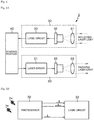
- Fig. 1 is a schematic configuration diagram showing a distance measurement device according to the embodiment of the present disclosure.
- a distance measurement device 1 according to the present embodiment adopts, as a measurement method for measuring a distance to a subject 10 that is a measurement object, a ToF method of measuring time until light (for example, laser light) having been emitted toward the subject 10 returns after being reflected by the subject 10.
- the distance measurement device 1 according to the present embodiment includes a light source 20 and a photodetection device 30.
- a photodetection device according to the embodiment of the present disclosure to be described later is used as the photodetection device 30.
- the light source 20 has a laser driver 21, a laser light source 22, and a diffusing lens 23 and radiates laser light toward the subject 10.
- the laser driver 21 drives the laser light source 22 under control of a control portion 40.
- the laser light source 22 is made of, for example, a semiconductor laser and emits laser light by being driven by the laser driver 21.
- the diffusing lens 23 diffuses laser light emitted from the laser light source 22 and radiates the diffused laser light toward the subject 10.
- the photodetection device 30 has a light-receiving lens 31, a photosensor 32, and a logic circuit 33 and receives reflected laser light that is returning radiated laser light from a laser radiating portion 20 after being reflected by the subject 10.
- the light-receiving lens 31 collects reflected laser light from the subject 10 on a light-receiving surface of the photosensor 32.
- the photosensor 32 receives the reflected laser light from the subject 10 via the light-receiving lens 31 in units of a pixel and photoelectrically converts the reflected laser light.
- An output signal of the photosensor 32 is supplied to the control portion 40 via the logic circuit 33. Details of the photosensor 32 will be described later.
- control portion 40 is constituted by a CPU (Central Processing Unit) or the like, controls the light source 20 and the photodetection device 30, and measures a time t until laser light having been emitted toward the subject 10 from the light source 20 returns after being reflected by the subject 10.
- a distance L to the subject 10 can be obtained based on the measured time t.
- the time t is measured by starting a timer at a timing where pulse light is emitted from the light source 20 and stopping the timer at a timing where the pulse light is received by the photodetection device 30.
- pulse light may be emitted from the light source 20 at a predetermined period, a period upon the photodetection device 30 receiving the pulse light may be detected, and the time t may be measured based on a phase difference between the period of light emission and the period of light reception.
- Time measurement is executed a plurality of times and the time t is measured by detecting a peak of a histogram created by stacking up a plurality of measured times.
- a two-dimensional array sensor (a so-called area sensor) constituted by pixels including a light-receiving element (a light-receiving portion) and being arranged in a two-dimensional array or a one-dimensional array sensor (a so-called line sensor) constituted by pixels including a light-receiving element and being arranged linearly can also be used.
- a sensor in which the light-receiving element of a pixel is constituted by an element that generates a signal in response to receiving a photon such as sensor made of a SPAD (Single Photon Avalanche Diode) element is used as the photosensor 32.
- the photodetection device 30 according to the present embodiment is configured such that the light-receiving element of a pixel is constituted by a SPAD element.
- the light-receiving element is not limited to a SPAD element and other various elements such as an APD (Avalanche Photo Diode) or a CAPD (Current Assisted Photonic Demodulator) may be used.
- a passive system that passively controls an avalanche current
- an active system that actively performs switching by controlling timings or the like.
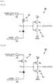
- a first example of the passive system is an example in which a load circuit 55 is constituted by a resistive element R.
- Fig. 3A shows the pixel circuit according to the first example of the passive system.
- a cathode electrode is connected via the resistive element R that is the load circuit 55 to a terminal 52 to which a power supply voltage V DD is applied and an anode electrode is connected to a terminal 53 to which an anode voltage V bd is applied.
- a cathode voltage V CA of the SPAD element 51 is derived as a SPAD output (a pixel circuit output) via a waveform shaping circuit 54 constituted by a P-type MOS transistor Q p and an N-type MOS transistor Q n .
- a voltage equal to or higher than a breakdown voltage V BD (for example, -50 to -10 V) is applied to the SPAD element 51.
- An excess voltage equal to or higher than the breakdown voltage V BD is referred to as an excess bias voltage V EX and is generally a voltage of around 2 to 5 V. This is a larger value than a conventional photodiode.
- the SPAD element 51 operates in a region called a Geiger mode that is devoid of a DC stabilization point.
- a second example of the passive system is an example in which the load circuit 55 is constituted by a constant-current source such as a P-type MOS transistor Q L .
- Fig. 3B shows the pixel circuit according to the second example of the passive system.
- the pixel circuit 50 according to the second example of the passive system only differs from the pixel circuit 50 according to the first example shown in Fig. 3A in that the load circuit 55 in the pixel circuit 50 according to the first example has been changed from the resistive element R to the P-type MOS transistor Q L and other circuit components are basically the same.
- Circuit operations of the pixel circuit 50 of the passive system configured as described above will be described using a waveform diagram shown in Fig. 4A .
- V DD - V bd In a state where a current does not flow through the SPAD element 51, a voltage of V DD - V bd is applied to the SPAD element 51.
- the voltage value (V DD - V bd ) equates to (V BD + V EX ).
- DCR dark Count Rate
- light radiation at the PN junction of the SPAD element 51 causes an avalanche multiplication to occur and an avalanche current I a is generated. This phenomenon probabilistically occurs even in a state where light is shielded (in other words, a state where there is no incident light). This is called a dark electron generation rate DCR.
- the cathode voltage V CA of the SPAD element 51 recovers from the quench voltage to the power supply voltage V DD and returns to its initial state.
- the load circuit 55 constituted by the resistive element R or the P-type MOS transistor Q L is a recharge circuit which supplies the SPAD element 51 with the recharge current I r in order to restore the cathode voltage V CA of the SPAD element 51.
- the incidence of even one photon can be detected at a certain probabilistic PDE (Photon Detection Efficiency).
- the probabilistic PDE at which a photon can be detected is usually around several % to 20%.
- a waveform of the cathode voltage V CA is shaped by the waveform shaping circuit 54 and a pulse signal with a pulse width T of which an arrival time of one photon is a start point becomes an SPAD output (a pixel circuit output).
- the SPAD element 51 is a high-performance photosensor capable of detecting the incidence of a single photon at a certain probabilistic PDE.
- a photon there is a period of several ns to several ten ns during which the SPAD element 51 cannot react to a photon as a photosensor or, in other words, a dead time DT. Therefore, when a detection frequency of photons rises under a high light intensity condition and a total period of the dead time DT becomes non-negligible with respect to observation time, photodetection accuracy declines.
- the avalanche current I a flows through the SPAD element 51 and, when the voltage applied to the SPAD element 51 decreases, the avalanche current I a stops by itself and a switch is made to a recharge operation in which the recharge current I r is supplied.
- the avalanche current I a flows in a section in which the cathode voltage V CA drops
- the recharge current I r starts to flow as the cathode voltage V CA starts to drop and, therefore, the cathode voltage V CA does not experience an excessive potential drop.
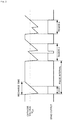
- the dead time DT during which the SPAD element 51 cannot react to photons as a photosensor will now be described in greater detail using a waveform diagram shown in Fig. 5 .
- a dead time DT attributable to a time required by the cathode voltage V CA to recover to the power supply voltage V DD in which incidence of light cannot be reacted to. For example, while an avalanche multiplication occurs twice and, accordingly, two pulse signals are generated as SPAD output in a region a, only one pulse signal is generated despite an avalanche multiplication occurring twice in a region b.
- the SPAD element 51 does not generate a SPAD output with respect to incidence of light that occurs after an initial reaction by the SPAD element 51 and until the cathode voltage V CA reaches or exceeds a threshold voltage of the waveform shaping circuit 54 of a subsequent stage.
- this period constitutes the dead time DT and a pulse width T represents a limit value thereof.
- FIG. 6 shows a pixel circuit of an active system.
- a pixel circuit 60 of the active system is configured to include, in addition to the SPAD element 51 and the waveform shaping circuit 54, a switch circuit 61, a delay circuit 62, and an inverter circuit 63.
- the switch circuit 61 is constituted by the terminal 52 to which the power supply voltage V DD is applied and, for example, a P-type MOS transistor Qs that is connected between the terminal 52 and a cathode electrode of the SPAD element 51.
- An input terminal of the delay circuit 62 is connected to an output terminal of the waveform shaping circuit 54.
- An input terminal of the inverter circuit 63 is connected to an output terminal of the delay circuit 62, and an output terminal of the inverter circuit 63 is connected to a gate electrode of the P-type MOS transistor Qs.
- Circuit operations of the pixel circuit 60 of the active system configured as described above will be described using a waveform diagram shown in Fig. 4B .
- an output of the waveform shaping circuit 54 or, in other words, a SPAD output is delayed by a predetermined amount of delay by the delay circuit 62, logically inverted by the inverter circuit 63, and applied to the gate electrode of the P-type MOS transistor Qs.
- the P-type MOS transistor Qs of the switch circuit 61 is to perform an on and off operation in accordance with the SPAD output.
- a recharge operation is performed with a large current after a desired time representing the amount of delay of the delay circuit 62 regardless of a state of potential of the SPAD element 51.
- the recharge current I r does not flow in a section in which the cathode voltage V CA drops.
- the avalanche current I a lowers the cathode voltage V CA
- a current value of the avalanche current I a is random, a lower limit voltage of the cathode voltage V CA varies and may end up excessively lowering the cathode voltage V CA .
- the avalanche current I a and the recharge current I r are switched on and off according to external signals, there is a high degree of freedom of timing control.
- the recharge current I r is not limited, there is an advantage that a dead time DT during which the pixel circuit 60 cannot react to a photon as a photosensor can be shortened down to a theoretical limit value.
- the recharge current I r may inadvertently flow through the SPAD element 51 before a quench operation is completed.
- a variation in the quench voltage causes the cathode voltage V CA of the SPAD element 51 to drop more than expected, and an overvoltage equal to or exceeding a rated value may be applied to a circuit element and cause the circuit element to deteriorate.
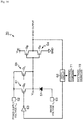
- a photodetection device is configured to include: a load circuit connected a SPAD element that is an example of a light-receiving element; a switch circuit connected to the SPAD element; and a feedback circuit configured to operate the switch circuit in accordance with an output from the SPAD element, wherein the feedback circuit includes a delay circuit.
- a first example represents an example of a hybrid recharge system which combines a passive circuit and an active circuit.
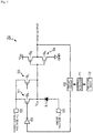
- Fig. 7 shows a circuit diagram of a pixel circuit in a photodetection device according to the first example.
- Fig. 7 illustrates a circuit configuration corresponding to one pixel.
- a pixel circuit 70 of the hybrid recharge system is configured to include, in addition to the SPAD element 51 and the waveform shaping circuit 54, the load circuit 55, the switch circuit 61, the delay circuit 62, the inverter circuit 63, a control portion 71, and a temperature sensor 72.
- the control portion 71 and the temperature sensor 72 are to be commonly provided with respect to a plurality of pixel circuits 70.
- the load circuit 55 is a recharge circuit of the passive system and the switch circuit 61 is a recharge circuit of the active system. Therefore, the recharge circuit of the pixel circuit 70 according to the first example represents a hybrid recharge circuit which combines a passive recharge circuit and an active recharge circuit.
- the resistive element R (refer to Fig. 3A ) may be used as the load circuit 55. This description similarly applies to the examples to be described later.
- the delay circuit 62 is provided midway along a path from the SPAD output to control input of the switch circuit 61 and forms a feedback circuit for active recharge.
- the delay circuit 62 is configured such that an amount of delay is variable.
- the amount of delay of the delay circuit 62 is controlled by the control portion 71.
- a delay circuit 62A according to the first circuit example and a delay circuit 62B according to the second circuit example are both configured such that two inverters IN 11 and IN 12 are cascade-connected and a capacitative element C is connected between a common connection node N of the two inverters IN 11 and IN 12 and a GND node that is a node of a reference potential.
- the inverter IN 11 is constituted by a P-type MOS transistor Q p1 and an N-type MOS transistor Q n1
- the inverter IN 12 is constituted by a P-type MOS transistor Q p2 and an N-type MOS transistor Q n2 .
- the delay circuit 62A according to the first circuit example has a variable current source I 11 which is connected between one end of the inverter IN 11 and a node of the power supply voltage V DD and of which a current value is variable and a variable current source I 11 which is connected between another end of the inverter IN 11 and the GND node and of which a current value is variable. Furthermore, with the delay circuit 62 according to the first circuit example, an amount of delay is adjusted by controlling current values of the variable current sources I 11 and I 12 . The current values of the variable current sources I 11 and I 12 are to be controlled under the control of the control portion 71.
- the delay circuit 62B according to the second circuit example has a constant-current source I 21 which is connected between one end of the inverter IN 11 and a node of the power supply voltage V DD and a constant-current source I 22 which is connected between another end of the inverter IN 11 and the GND node. Furthermore, the delay circuit 62 according to the second circuit example has a variable capacitative element VC of which a capacitance value is variable in place of the capacitative element C, and an amount of delay of the delay circuit 62 is adjusted by controlling the capacitance value of the variable capacitative element VC. The capacitance value of the variable capacitative element VC is to be controlled under the control of the control portion 71.
- the control portion 71 controls an amount of delay of a delay circuit in accordance with an element characteristic of the SPAD element 51.
- an element characteristic of the SPAD element 51 a temperature of the SPAD element 51 or, specifically, a junction temperature can be exemplified.
- the temperature sensor 72 detects the temperature of the SPAD element 51.
- the photodetection device has a laminated structure made by laminating at least two semiconductor substrates, namely, a first semiconductor substrate and a second semiconductor substrate, the SPAD element 51 is arranged in a two-dimensional array on the first semiconductor substrate, and circuit portions other than the SPAD element 51 such as the pixel circuit 50 are arranged on the second semiconductor substrate.
- the temperature sensor 72 can detect a temperature of the SPAD element 51 by being mounted on the second semiconductor substrate.
- a known temperature sensor can be used which measures a temperature by utilizing characteristics that electric properties change in proportion to a temperature change in a bandgap of a semiconductor.
- the control portion 71 adopts the temperature (specifically, the junction temperature) of the SPAD element 51 that is detected by the temperature sensor 72 as the element characteristic and adjusts the amount of delay of the delay circuit 62 in accordance with the element characteristic.
- the pixel circuit 70 according to the first example is constituted by a combination of a passive recharge circuit and an active recharge circuit, and by adjusting the amount of delay of the delay circuit 62 in accordance with the temperature of the SPAD element 51 that is detected by the temperature sensor 72, a variation in the junction temperature is suppressed. Accordingly, a risk of an excessive drop in the cathode voltage V CA causing an overvoltage equal to or exceeding a rated value to be applied to circuit elements can be reduced while realizing a short dead time DT.
- Fig. 9A shows a waveform diagram of the cathode voltage V CA and the SPAD output in a case where the dead time DT is short
- Fig. 9B shows a waveform diagram of the cathode voltage V CA and the SPAD output in a case where the dead time DT is long.
- a second example is a modification of the first example and represents an example of adjusting the amount of delay based on a voltage monitoring result.
- Fig. 10 shows a circuit diagram of a pixel circuit in a photodetection device according to the second example.
- the amount of delay of the delay circuit 62 is controlled in accordance with a temperature of the SPAD element 51 in the first example
- a fluctuation of the power supply voltage V DD is monitored and the amount of delay of the delay circuit 62 is controlled in accordance with a voltage monitoring result thereof.
- the pixel circuit 70 according to the second example is configured to include a voltage monitor 73 that monitors a fluctuation in the power supply voltage V DD in place of the temperature sensor 72 that detects a temperature of the SPAD element 51.
- the control portion 71 adjusts the amount of delay of the delay circuit 62 based on a monitoring result of the voltage monitor 73.
- the pixel circuit 70 according to the second example is constituted by a combination of a passive recharge circuit and an active recharge circuit, and by adjusting the amount of delay of the delay circuit 62 based on a monitoring result of the voltage monitor 73, a fluctuation in the power supply voltage V DD is suppressed. Accordingly, in a similar manner to the first example, a risk of an excessive drop in the cathode voltage V CA causing an overvoltage equal to or exceeding a rated value to be applied to circuit elements can be reduced while realizing a short dead time DT.
- a third example is a modification of the first example and represents an example of including a comparator in a feedback circuit.
- Fig. 11 shows a circuit diagram of a pixel circuit in a photodetection device according to the third example.
- the pixel circuit 70 according to the third example is configured to include a comparator 74 in a feedback circuit for active recharge. More specifically, in the pixel circuit 70 according to the third example which is constituted by a combination of a passive recharge circuit and an active recharge circuit, a circuit (a path) from the SPAD output to the control input of the switch circuit 61 is a feedback circuit for performing active recharge based on the SPAD output. In addition, besides the delay circuit 62, the feedback circuit further includes the comparator 74.
- the comparator 74 receives the cathode voltage V CA of the SPAD element 51 as a comparison input (one of inputs), receives a reference voltage V ref that is generated by a reference voltage generating portion 75 as a comparison reference input (the other input), and compares the cathode voltage V CA with the reference voltage V ref .
- a comparison result of the comparator 74 or, in other words, an analog-digital transformation result is supplied to the delay circuit 62 as an input thereof and, at the same time, derived as a SPAD output that is a pixel circuit output.
- the reference voltage V ref that is generated by the reference voltage generating portion 75 is configured so that a voltage value thereof is variable.
- the pixel circuit 70 according to the third example is the pixel circuit 70 according to the first example but including the comparator 74 in a feedback circuit for active recharge and having been configured such that a voltage value of the reference voltage V ref of the comparator 74 is variable.
- a level of analog-digital transformation in the comparator 74 can be adjusted.
- a fourth example is a modification of the third example and represents a configuration example provided with separate paths for a SPAD output and an active recharge.
- Fig. 12 shows a circuit diagram of a pixel circuit in a photodetection device according to the fourth example.
- a configuration is adopted in which a comparison result of the comparator 74 is derived as the SPAD output and supplied to the switch circuit 61 via the delay circuit 62 inside the feedback circuit.
- the pixel circuit 70 according to the fourth example is configured such that a path for deriving the SPAD output that is a pixel circuit output is separated from a path that includes a feedback circuit for active recharge.
- a configuration is adopted in which the path including the feedback circuit is provided as a separate path from the path for deriving the SPAD output.
- the cathode voltage V CA of the SPAD element 51 is derived as the SPAD output via the waveform shaping circuit 54.
- the comparator 74 is configured to receive the cathode voltage V CA of the SPAD element 51 as an input and supply a comparison result thereof to the switch circuit 61 via the delay circuit 62 inside the feedback circuit.
- the technique according to the present disclosure has been heretofore described based on a preferable embodiment, the technique according to the present disclosure is not limited to the embodiment.
- Configurations and structures of an imaging device described in the embodiment presented above are exemplary and various modifications can be made thereto as deemed appropriate.
- the embodiment presented above has been described using examples in which a SPAD element is used as a light-receiving element, the light-receiving element is not limited to a SPAD element and similar operational advantages can be obtained using an element such as an APD or a CAPD.
- the technique according to the present disclosure can be applied to various products.
- the technique according to the present disclosure may be realized as a distance measurement device to be mounted to any of various types of mobile bodies including an automobile, an electric vehicle, a hybrid electric vehicle, a motorcycle, a bicycle, personal mobility, an airplane, a drone, an ocean vessel, a robot, construction machinery, and agricultural and farm machinery (a tractor).
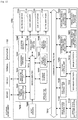
- Fig. 13 is a block diagram showing a schematic configuration example of a vehicle control system 7000 that represents an example of a mobile body control system to which the technique according to the present disclosure may be applied.
- the vehicle control system 7000 includes a plurality of electronic control units that are connected via a communication network 7010.
- the vehicle control system 7000 includes a drive system control unit 7100, a body system control unit 7200, a battery control unit 7300, an external vehicle information detecting unit 7400, an internal vehicle information detecting unit 7500, and an integrated control unit 7600.
- the communication network 7010 that connects the plurality of control units may be a vehicle-mounted communication network compliant with an arbitrary standard such as a CAN (Controller Area Network), a LIN (Local Interconnect Network), a LAN (Local Area Network), or FlexRay (registered trademark).
- CAN Controller Area Network
- LIN Local Interconnect Network
- LAN Local Area Network
- FlexRay registered trademark
- Each control unit includes a microcomputer that performs arithmetic processing in accordance with various programs, a storage portion that stores programs to be executed by the microcomputer, parameters to be used in various calculations, and the like, and a drive circuit that drives various apparatuses which are control targets.
- Each control unit includes a network I/F for communicating with other control units via the communication network 7010 and a communication I/F for communicating with apparatuses, sensors, and the like inside and outside the vehicle via wired communication or wireless communication.
- FIG. 13 illustrates, as functional components of the integrated control unit 7600, a microcomputer 7610, a general-purpose communication I/F 7620, a dedicated communication I/F 7630, a positioning portion 7640, a beacon receiving portion 7650, an on-board device I/F 7660, an audio/video output portion 7670, a vehicle-mounted network I/F 7680, and a storage portion 7690.
- the other control units similarly include a microcomputer, a communication I/F, a storage portion, and the like.
- the drive system control unit 7100 controls operations of apparatuses related to a drive system of a vehicle in accordance with various programs.
- the drive system control unit 7100 functions as a control apparatus of a drive force generation apparatus for generating a drive force of the vehicle such as an internal engine or a drive motor, a control apparatus of a drive force transmission mechanism for transmitting the drive force to wheels, a control apparatus of a steering mechanism for adjusting a steering angle of the vehicle, and a control apparatus of a braking apparatus that generates a brake force of the vehicle.
- the drive system control unit 7100 may have functions as a control apparatus of an ABS (Antilock Brake System), a control apparatus of ESC (Electronic Stability Control), or the like.
- a vehicle state detecting portion 7110 is connected to the drive system control unit 7100.
- the vehicle state detecting portion 7110 includes at least one of a gyroscope sensor that detects an angular velocity of a rotational motion of a shaft of a vehicle body, an acceleration sensor that detects an acceleration of the vehicle, and a sensor for detecting an operation amount of a gas pedal, an operation amount of a brake pedal, a steering angle of a steering wheel, the number of revolutions of an engine, a rotational speed of a wheel, or the like.
- the drive system control unit 7100 performs arithmetic processing using a signal input from the vehicle state detecting portion 7110 and controls an internal engine, a drive motor, an electric power steering apparatus, a brake apparatus, or the like.
- the body system control unit 7200 controls operations of various apparatuses mounted to the vehicle body in accordance with various programs.
- the body system control unit 7200 functions as a control apparatus of a key-less entry system, a smart key system, a power window apparatus, or various lamps such as head lamps, tail lamps, brake lamps, turn indicators, and fog lamps.
- radio waves or signals of various switches which are transmitted from a portable device that substitutes as a key may be input to the body system control unit 7200.
- the body system control unit 7200 accepts input of the radio waves or signals and controls a door lock apparatus, the power window apparatus, the lamps, and the like of the vehicle.
- the battery control unit 7300 controls a secondary battery 7310 that is a power supply source of the drive motor in accordance with various programs. For example, information on a battery temperature, a battery output voltage, a battery remaining capacity, or the like is input to the battery control unit 7300 from a battery apparatus including the secondary battery 7310. The battery control unit 7300 uses these signals to perform arithmetic processing to control temperature regulation of the secondary battery 7310 or to control a cooling apparatus or the like included in the battery apparatus.
- the external vehicle information detecting unit 7400 detects information on an exterior of the vehicle that is mounted with the vehicle control system 7000.
- an imaging portion 7410 and an external vehicle information detecting portion 7420 is connected to the external vehicle information detecting unit 7400.
- the imaging portion 7410 includes at least one of a ToF (Time of Flight) camera, a stereo camera, a monocular camera, an infrared camera, and other cameras.
- the external vehicle information detecting portion 7420 includes at least one of an environmental sensor for detecting present weather or meteorological phenomena and an ambient information detection sensor for detecting other vehicles, obstacles, pedestrians, or the like around the vehicle mounted with the vehicle control system 7000.
- the environmental sensor may be at least one of a raindrop sensor that detects rainy weather, a fog sensor that detects fog, a sunshine sensor that detects a degree of sunshine, and a snow sensor that detects snowfall.
- the ambient information detection sensor may be at least one of an ultrasonic sensor, a radar apparatus, and a LIDAR (Light Detection and Ranging, Laser Imaging Detection and Ranging) apparatus.
- the imaging portion 7410 and the external vehicle information detecting portion 7420 may be respectively included as an independent sensor or an independent apparatus or may be included as an apparatus that integrates a plurality of sensors or apparatuses.
- Fig. 14 shows an example of installation positions of the imaging portion 7410 and the external vehicle information detecting portion 7420.
- imaging portions 7910, 7912, 7914, 7916, and 7918 are provided at least one position among a front nose, a side mirror, a rear bumper, a rear door, and an upper part of a front glass inside a cabin of a vehicle 7900.
- the imaging portion 7910 that is provided on the front nose and the imaging portion 7918 that is provided in the upper part of the front glass inside the cabin mainly acquire an image of the front of the vehicle 7900.
- the imaging portions 7912 and 7914 that are provided on the side mirrors mainly acquire an image of the sides of the vehicle 7900.
- the imaging portion 7916 that is provided on the rear bumper or the rear door mainly acquires an image of the rear of the vehicle 7900.
- the imaging portion 7918 that is provided in the upper part of the front glass inside the cabin is mainly used to detect vehicles ahead, pedestrians, obstacles, traffic lights, traffic signs, lanes, and the like.
- Fig. 14 shows an example of photographic ranges of the respective imaging portions 7910, 7912, 7914, and 7916.
- An imaging range a represents an imaging range of the imaging portion 7910 that is provided on the front nose
- imaging ranges b and c respectively represent imaging ranges of the imaging portions 7912 and 7914 that are provided on the side mirrors
- an imaging range d represents an imaging range of the imaging portion 7916 that is provided on the rear bumper or the rear door.
- external vehicle information detecting portions 7920, 7922, 7924, 7926, 7928, and 7930 that are provided in the front, the rear, the sides, a corner, and the upper part of the front glass inside the cabin of the vehicle 7900 may be ultrasonic sensors or radar apparatuses.
- the external vehicle information detecting portions 7920, 7926, and 7930 that are provided on the front nose, the rear bumper, the rear door, and the upper part of the front glass inside the cabin of the vehicle 7900 may be LIDAR apparatuses.
- the external vehicle information detecting portions 7920 to 7930 are mainly used to detect vehicles ahead, pedestrians, obstacles, and the like.
- the external vehicle information detecting unit 7400 causes the imaging portion 7410 to capture an image of the exterior of the vehicle and receives captured image data.
- the external vehicle information detecting unit 7400 receives detection information from the external vehicle information detecting portion 7420 being connected thereto.
- the external vehicle information detecting portion 7420 is an ultrasonic sensor, a radar apparatus, or a LIDAR apparatus
- the external vehicle information detecting unit 7400 causes the external vehicle information detecting portion 7420 to transmit ultrasonic waves, electromagnetic waves, or the like and receives information on received reflected waves.
- the external vehicle information detecting unit 7400 may perform object detection processing or distance detection processing with respect to people, vehicles, obstacles, signs, characters on road surfaces, and the like. Based on the received information, the external vehicle information detecting unit 7400 may perform environmental recognition processing for recognizing rainfall, fog, road surface conditions, or the like. Based on the received information, the external vehicle information detecting unit 7400 may calculate a distance to an object outside of the vehicle.
- the external vehicle information detecting unit 7400 may perform image recognition processing or distance detection processing for recognizing people, vehicles, obstacles, signs, characters on road surfaces, and the like.
- the external vehicle information detecting unit 7400 may perform processing such as distortion correction or positioning with respect to the received image data and composite the pieces of image data captured by different imaging portions 7410 to generate a bird's-eye view image or a panoramic image.
- the external vehicle information detecting unit 7400 may perform viewpoint transformation processing using pieces of image data captured by different imaging portions 7410.
- the internal vehicle information detecting unit 7500 detects information on an interior of the vehicle.
- a driver state detecting portion 7510 that detects a state of a driver is connected to the internal vehicle information detecting unit 7500.
- the driver state detecting portion 7510 may include a camera that captures an image of the driver, a biometric sensor that detects biological information of the driver, a microphone that collects sound inside the cabin, or the like.
- the biometric sensor is provided on a seat surface, the steering wheel, or the like, and detects biological information of a passenger sitting on the seat or the driver holding the steering wheel.
- the internal vehicle information detecting unit 7500 may calculate a degree of fatigue or a degree of concentration of the driver or may determine whether or not the driver has fallen asleep.
- the internal vehicle information detecting unit 7500 may perform processing such as noise cancellation processing with respect to a collected sound signal.
- the integrated control unit 7600 controls overall operations in the vehicle control system 7000 in accordance with various programs.
- An input portion 7800 is connected to the integrated control unit 7600.
- the input portion 7800 is realized by an apparatus on which a passenger can perform input operations such as a touch panel, a button, a microphone, a switch, or a lever. Data obtained by subjecting sound input from the microphone to speech recognition may be input to the integrated control unit 7600.
- the input portion 7800 may be a remote-controlled apparatus using infrared light or other radio waves or an externally-connected device such as a mobile phone or a PDA (Personal Digital Assistant) that accommodates operations of the vehicle control system 7000.
- PDA Personal Digital Assistant
- the input portion 7800 may be a camera, in which case a passenger can input information by gesturing to the camera.
- data obtained by detecting a motion of a wearable apparatus being worn by a passenger may be input.
- the input portion 7800 described above may include an input control circuit or the like which generates an input signal based on information input by a passenger or the like using the input portion 7800 and which outputs the generated input signal to the integrated control unit 7600.
- a passenger or the like inputs various types of data and issues instructions to perform processing operations with respect to the vehicle control system 7000.
- the storage portion 7690 may include a ROM (Read Only Memory) that stores various programs to be executed by the microcomputer and a RAM (Random Access Memory) that stores various parameters, calculation results, sensor values, or the like.
- the storage portion 7690 may be realized by a magnetic storage device such as an HDD (Hard Disk Drive), a semiconductor storage device, an optical storage device, a magneto-optical storage device, or the like.
- the general-purpose communication I/F 7620 is a general-purpose communication I/F that mediates communication with various devices that are present in an external environment 7750.
- the general-purpose communication I/F 7620 may implement a cellular communication protocol such as GSM (registered trademark) (Global System of Mobile communications), WiMAX, LTE (Long Term Evolution), or LTE-A (LTE-Advanced) or another wireless communication protocol such as wireless LAN (also referred to as Wi-Fi (registered trademark)) or Bluetooth (registered trademark).
- GSM Global System of Mobile communications
- WiMAX Wireless LAN
- LTE-A Long Term Evolution-Advanced
- wireless LAN also referred to as Wi-Fi (registered trademark)
- Bluetooth registered trademark
- the general-purpose communication I/F 7620 may connect to a device (for example, an application server or a control server) present on an external network (for example, the Internet, a cloud network, or a company-specific network) via a base station or an access point.
- a device for example, an application server or a control server
- an external network for example, the Internet, a cloud network, or a company-specific network
- the general-purpose communication I/F 7620 may connect to a terminal (for example, a terminal belonging to a driver, a pedestrian, a terminal of a store, or an MTC (Machine Type Communication) terminal) that is present in a vicinity of the vehicle using P2P (Peer To Peer) technology.
- P2P Peer To Peer
- the dedicated communication I/F 7630 is a communication I/F that supports a communication protocol designed to be used in a vehicle.
- the dedicated communication I/F 7630 may implement a standard protocol such as WAVE (Wireless Access in Vehicle Environment) that is a combination of IEEE 802.11p constituting a lower layer and IEEE 1609 constituting a higher layer, DSRC (Dedicated Short Range Communications), or a cellular communication protocol.
- WAVE Wireless Access in Vehicle Environment
- DSRC Dedicated Short Range Communications
- the dedicated communication I/F 7630 carries out V2X communication that is a concept including one or more of communication between vehicles (Vehicle to Vehicle communication), communication between a road and a vehicle (Vehicle to Infrastructure communication), communication between a vehicle and a home (Vehicle to Home communication), and communication between a pedestrian and a vehicle (Vehicle to Pedestrian communication).
- V2X communication is a concept including one or more of communication between vehicles (Vehicle to Vehicle communication), communication between a road and a vehicle (Vehicle to Infrastructure communication), communication between a vehicle and a home (Vehicle to Home communication), and communication between a pedestrian and a vehicle (Vehicle to Pedestrian communication).
- the positioning portion 7640 receives a GNSS (Global Navigation Satellite System) signal from a GNSS satellite (for example, a GPS (Global Positioning System) signal from a GPS satellite) and executes positioning, and generates positional information including a latitude, a longitude, and an elevation of the vehicle.
- a GNSS Global Navigation Satellite System
- GPS Global Positioning System
- the positioning portion 7640 may specify a current position by exchanging signals with a wireless access point or acquire positional information from a terminal such as a mobile phone, a PHS, or a smartphone with a positioning function.
- the beacon receiving portion 7650 receives radio waves or electromagnetic waves emitted from a radio station or the like installed on a road and acquires information such as a current position, congestions, closures, and required time.
- the function of the beacon receiving portion 7650 may be included in the dedicated communication I/F 7630 described above.
- the on-board device I/F 7660 is a communication interface that mediates communication between the microcomputer 7610 and various on-board devices 7760 that are present inside the vehicle.
- the on-board device I/F 7660 may establish a wireless connection using a wireless communication protocol such as a wireless LAN, Bluetooth (registered trademark), NFC (Near Field Communication), or WUSB (Wireless USB).
- a wireless communication protocol such as a wireless LAN, Bluetooth (registered trademark), NFC (Near Field Communication), or WUSB (Wireless USB).
- the on-board device I/F 7660 may establish, via a connection terminal (not illustrated) (and a cable when necessary), a wired connection such as USB (Universal Serial Bus), HDMI (registered trademark) (High-Definition Multimedia Interface), or MHL (Mobile High-definition Link).
- USB Universal Serial Bus
- HDMI registered trademark
- MHL Mobile High-definition Link
- the on-board devices 7760 may include at least one of a mobile device or a wearable device that is held or worn by a passenger and an information device to be carried onto or attached to the vehicle. Furthermore, the on-board devices 7760 may include a navigation apparatus that searches a route to an arbitrary destination.
- the on-board device I/F 7660 exchanges control signals and data signals with the on-board devices 7760.
- the vehicle-mounted network I/F 7680 is an interface that mediates communication between the microcomputer 7610 and the communication network 7010.
- the vehicle-mounted network I/F 7680 transmits and receives signals and the like in accordance with a prescribed protocol that is supported by the communication network 7010.
- the microcomputer 7610 of the integrated control unit 7600 controls the vehicle control system 7000 in accordance with various programs based on information acquired via at least one of the general-purpose communication I/F 7620, the dedicated communication I/F 7630, the positioning portion 7640, the beacon receiving portion 7650, the on-board device I/F 7660, and the vehicle-mounted network I/F 7680. For example, based on acquired information on the exterior and the interior of the vehicle, the microcomputer 7610 may calculate a control target value of the drive force generation apparatus, the steering mechanism, or the brake apparatus and output a control command to the drive system control unit 7100.
- the microcomputer 7610 may perform cooperative control for the purpose of realizing functions of an ADAS (Advanced Driver Assistance System) including collision avoidance or crash mitigation of the vehicle, headway control based on an inter-vehicular distance, cruise control, a collision warning of the vehicle, and a lane departure warning of the vehicle.
- ADAS Advanced Driver Assistance System
- the microcomputer 7610 may perform cooperative control for the purpose of automated driving or the like that enables the vehicle to travel autonomously without having to rely on operations by the driver.
- the microcomputer 7610 may generate three-dimensional distance information between the vehicle and a surrounding object such as a structure or a person and create local map information including peripheral information of a current position of the vehicle based on information acquired via at least one of the general-purpose communication I/F 7620, the dedicated communication I/F 7630, the positioning portion 7640, the beacon receiving portion 7650, the on-board device I/F 7660, and the vehicle-mounted network I/F 7680.
- the microcomputer 7610 may predict danger such as a collision involving the vehicle, an approach by a pedestrian or the like, or entering a closed road and generate a warning signal.
- the warning signal may be a signal for generating a warning sound or turning on a warning lamp.
- the audio/video output portion 7670 transmits an output signal of at least one of sound and an image to an output apparatus that is capable of audibly or visually notifying a passenger of the vehicle or the outside of the vehicle of information.
- an audio speaker 7710, a display portion 7720, and an instrument panel 7730 are exemplified as output apparatuses.
- the display portion 7720 may include at least one of an on-board display and a head-up display.
- the display portion 7720 may have an AR (Augmented Reality) display function.
- the output apparatus may be an apparatus other than those described above such as headphones, a wearable device such as a spectacle-type display to be worn by a passenger, a projector, or a lamp.
- the output apparatus When the output apparatus is a display apparatus, the display apparatus visually displays, in various formats such as a text, an image, a table, and a graph, results obtained by various types of processing performed by the microcomputer 7610 and information received from other control units.
- the output apparatus is an audio output apparatus, the audio output apparatus converts an audio signal constituted by reproduced speech data, acoustic data, or the like into an analog signal and auditorially outputs the converted analog signal.
- At least two control units connected via the communication network 7010 may be integrated as a single control unit.
- each control unit may be constituted by a plurality of control units.
- the vehicle control system 7000 may include other control units that are not illustrated.
- a part of or all of the functions assumed by any control unit in the description provided above may be shouldered by another control unit.
- prescribed arithmetic processing may be performed by any control unit.
- a sensor or an apparatus connected to any control unit may be connected to another control unit and, at the same time, a plurality of control units may mutually transmit and receive detection information via the communication network 7010.
- the technique according to the present disclosure may be applied to, for example, the imaging portions 7910, 7912, 7914, 7916, and 7918 and external vehicle information detecting portions 7920, 7922, 7924, 7926, 7928, and 7930 among the configuration described above.
- the technique according to the present disclosure since a risk of an overvoltage being applied to a circuit element can be eliminated while maintaining advantages of the active system, deterioration of characteristics of the circuit element can be suppressed and a photodetection device with high reliability can be realized. Furthermore, mounting the photodetection device enables, example, a vehicle control system capable of detecting an imaging object with high accuracy to be constructed.
- the present disclosure can also be configured as follows.
Landscapes
- Engineering & Computer Science (AREA)
- Physics & Mathematics (AREA)
- Computer Networks & Wireless Communication (AREA)
- General Physics & Mathematics (AREA)
- Radar, Positioning & Navigation (AREA)
- Remote Sensing (AREA)
- Electromagnetism (AREA)
- Optical Radar Systems And Details Thereof (AREA)
- Measurement Of Optical Distance (AREA)
- Electronic Switches (AREA)
Abstract
Description
- The present disclosure relates to a photodetection device and a distance measurement device.
- As a light-receiving element (a light-receiving portion) that performs photodetection, there are distance measurement devices using an element that generates a signal in response to receiving a photon (for example, refer to PTL 1). With the distance measurement device according to conventional art, based on a measurement result of a ToF (Time of Flight), the number of pulses is detected when light intensity is low but a width of the pulses is detected when light intensity is high.
- [PTL 1]
JP 2014-081254 A - A photodetection operation using a light-receiving element that generates a signal in response to receiving a photon is, for example, a photodetection operation using a SPAD (Single Photon Avalanche Diode) element and is performed by repetitively generating/suspending an avalanche current. In addition, recovery of a cathode voltage that is lowered by the avalanche current is performed by a recharge circuit connected to the light-receiving element.
- There are two systems of pixel circuits including a light-receiving element: a passive system that passively controls an avalanche current; and an active system that actively performs switching by controlling timings or the like. While the active system has a higher degree of freedom of adjustment than the passive system, contrarily, unless timing control is performed accurately, there is a possibility that a malfunction may occur or an overvoltage equal to or exceeding a rated value may be applied to a circuit element and cause the circuit element to deteriorate.
-
PTL 1 described above discloses a pixel circuit adopting the passive system. Therefore, the conventional art described inPTL 1 does not take into consideration the risk inherent to the active system described above or, more specifically, the risk of a circuit element being subjected to an overvoltage. - An object of the present disclosure is to provide a photodetection device capable of reducing the risk of a circuit element being subjected to an overvoltage while maintaining advantages of an active system and a distance measurement device that includes the photodetection device.
- A photodetection device according to the present disclosure for achieving the object described above includes:
- a light-receiving element;
- a load circuit connected to the light-receiving element;
- a switch circuit connected to the light-receiving element; and
- a feedback circuit configured to operate the switch circuit in accordance with an output from the light-receiving element, wherein
- the feedback circuit has a delay circuit.
- In addition, a distance measurement device (a distance-measuring device) according to the present disclosure for achieving the object described above includes:
- a light source configured to radiate light toward a measurement object with; and
- a photodetection device configured to detect light reflected by the measurement object, wherein
- the photodetection device configured as described above is used as the photodetection device.
-
- [
Fig. 1 ]
Fig. 1 is a schematic configuration diagram showing a distance measurement device according to an embodiment of the present disclosure. - [
Fig. 2 ]
Figs. 2A and 2B are block diagrams showing a specific configuration of the distance measurement device according to the embodiment of the present disclosure. - [
Fig. 3 ]
Fig. 3A is a circuit diagram showing a pixel circuit according to a first example of a passive system, andFig. 3B is a circuit diagram showing a pixel circuit according to a second example of the passive system. - [
Fig. 4 ]
Fig. 4A is a waveform diagram for explaining a circuit operation of a pixel circuit of a passive system, andFig. 4B is a waveform diagram for explaining a circuit operation of a pixel circuit of an active system. - [
Fig. 5 ]
Fig. 5 is a waveform diagram for explaining a dead time DT of a SPAD element when a radiating light amount is relatively small. - [
Fig. 6 ]
Fig. 6 is a circuit diagram showing a pixel circuit of an active system. - [
Fig. 7 ]
Fig. 7 is a circuit diagram showing a pixel circuit in a photodetection device according to a first example. - [
Fig. 8 ]
Fig. 8A is a circuit diagram showing a first circuit example of a delay circuit of which an amount of delay is variable, andFig. 8B is a circuit diagram showing a second circuit example of the same. - [
Fig. 9 ]
Fig. 9A is a waveform diagram of a cathode voltage and a SPAD output in a case where a dead time DT is short, andFig. 9B is a waveform diagram of the cathode voltage and the SPAD output in a case where the dead time DT is long. - [
Fig. 10 ]
Fig. 10 is a circuit diagram showing a pixel circuit in a photodetection device according to a second example. - [
Fig. 11 ]
Fig. 11 is a circuit diagram showing a pixel circuit in a photodetection device according to a third example. - [
Fig. 12 ]
Fig. 12 is a circuit diagram showing a pixel circuit in a photodetection device according to a fourth example. - [
Fig. 13 ]
Fig. 13 is a block diagram showing a schematic configuration example of a vehicle control system that represents an example of a mobile body control system to which the technique according to the present disclosure may be applied. - [
Fig. 14 ]
Fig. 14 is a diagram showing an example of an installation position of a distance measurement device. - Hereinafter, a mode (hereinafter, referred to as an embodiment) for implementing the technique according to the present disclosure will be described in detail with reference to the drawings. It is to be understood that the technique according to the present disclosure is not limited to the embodiment and various numerical values and the like in the embodiment are exemplary. In the following description, a same reference sign will be used for a same element or elements having a same function and redundant descriptions will be omitted. The description will be given in the following order.
- 1. General description of photodetection device and distance measurement device according to present disclosure
- 2. Distance measurement device according to embodiment
- 2-1. Outline of configuration of distance measurement device
- 2-2. Basic pixel circuit of photodetection device using SPAD element
- 2-2-1. Pixel circuit according to first example of passive system
- 2-2-2. Pixel circuit according to second example of passive system
- 2-2-3. Circuit operations of pixel circuit of passive system
- 2-2-4. Dead time DT
- 2-2-5. Pixel circuit of active system
- 2-2-6. Circuit operations of pixel circuit of active system
- 3. Photodetection device according to embodiment
- 3-1. First example (example combining passive circuit and active circuit)
- 3-2. Second example (modification of first example: example of adjusting amount of delay based on voltage monitoring result)
- 3-3. Third example (modification of first example: example of including comparator in feedback circuit)
- 3-4. Fourth example (modification of third example: configuration example provided with separate paths for SPAD output and active recharge)
- 4. Example of application of technique according to present disclosure (example of mobile body)
- 5. Configurations adoptable by present disclosure
- With the photodetection device and the distance measurement device according to the present disclosure, a delay circuit can be configured such that an amount of delay is variable. In addition, a configuration can be adopted in which the amount of delay of the delay circuit is controlled in accordance with an element characteristic of the light-receiving element. A mode can be adopted in which the element characteristic of the light-receiving element is a temperature of the light-receiving element.
- With the photodetection device and the distance measurement device according to the present disclosure including the preferable mode and configuration described above, a configuration can be adopted in which the amount of delay of the delay circuit is controlled based on a monitoring result of a fluctuation of a power supply voltage.
- In addition, with the photodetection device and the distance measurement device according to the present disclosure including the preferable modes and configurations described above, a configuration can be adopted in which the feedback circuit further includes a comparator. The comparator can be configured to receive an output from the light-receiving element as a comparison input, receive a reference voltage as a comparison reference input, and provide the delay circuit with a comparison result thereof as an input. In addition, a configuration can be adopted in which a voltage value of the reference voltage of the comparator is variable.
- Furthermore, with the photodetection device and the distance measurement device according to the present disclosure including the preferable modes and configurations described above, a configuration can be adopted in which the comparison result of the comparator is derived as a pixel circuit output based on an output of the light-receiving element. Alternatively, a configuration can be adopted in which a path including the feedback circuit is a separate path from a path for deriving an output of the light-receiving element as a pixel circuit output.
- Furthermore, with the photodetection device and the distance measurement device according to the present disclosure including the preferable modes and configurations described above, a configuration can be adopted in which the light-receiving element is an element configured to generate a signal in accordance with the reception of a photon. Moreover, a configuration can be adopted in which the light-receiving element is constituted by a single photon avalanche diode.
-
Fig. 1 is a schematic configuration diagram showing a distance measurement device according to the embodiment of the present disclosure. Adistance measurement device 1 according to the present embodiment adopts, as a measurement method for measuring a distance to a subject 10 that is a measurement object, a ToF method of measuring time until light (for example, laser light) having been emitted toward the subject 10 returns after being reflected by the subject 10. In order to realize distance measurement by the ToF method, thedistance measurement device 1 according to the present embodiment includes alight source 20 and aphotodetection device 30. In addition, a photodetection device according to the embodiment of the present disclosure to be described later is used as thephotodetection device 30. -
Figs. 2A and 2B show a specific configuration of thedistance measurement device 1 according to the present embodiment. For example, thelight source 20 has alaser driver 21, alaser light source 22, and a diffusinglens 23 and radiates laser light toward the subject 10. Thelaser driver 21 drives thelaser light source 22 under control of acontrol portion 40. Thelaser light source 22 is made of, for example, a semiconductor laser and emits laser light by being driven by thelaser driver 21. The diffusinglens 23 diffuses laser light emitted from thelaser light source 22 and radiates the diffused laser light toward the subject 10. - The
photodetection device 30 has a light-receivinglens 31, aphotosensor 32, and alogic circuit 33 and receives reflected laser light that is returning radiated laser light from alaser radiating portion 20 after being reflected by the subject 10. The light-receivinglens 31 collects reflected laser light from the subject 10 on a light-receiving surface of thephotosensor 32. Thephotosensor 32 receives the reflected laser light from the subject 10 via the light-receivinglens 31 in units of a pixel and photoelectrically converts the reflected laser light. An output signal of thephotosensor 32 is supplied to thecontrol portion 40 via thelogic circuit 33. Details of the photosensor 32 will be described later. - For example, the
control portion 40 is constituted by a CPU (Central Processing Unit) or the like, controls thelight source 20 and thephotodetection device 30, and measures a time t until laser light having been emitted toward the subject 10 from thelight source 20 returns after being reflected by the subject 10. A distance L to the subject 10 can be obtained based on the measured time t. - As a method of measuring the time t, the time t is measured by starting a timer at a timing where pulse light is emitted from the
light source 20 and stopping the timer at a timing where the pulse light is received by thephotodetection device 30. As another method of time measurement, pulse light may be emitted from thelight source 20 at a predetermined period, a period upon thephotodetection device 30 receiving the pulse light may be detected, and the time t may be measured based on a phase difference between the period of light emission and the period of light reception. Time measurement is executed a plurality of times and the time t is measured by detecting a peak of a histogram created by stacking up a plurality of measured times. - As the
photosensor 32, a two-dimensional array sensor (a so-called area sensor) constituted by pixels including a light-receiving element (a light-receiving portion) and being arranged in a two-dimensional array or a one-dimensional array sensor (a so-called line sensor) constituted by pixels including a light-receiving element and being arranged linearly can also be used. - In addition, in the present embodiment, a sensor in which the light-receiving element of a pixel is constituted by an element that generates a signal in response to receiving a photon such as sensor made of a SPAD (Single Photon Avalanche Diode) element is used as the
photosensor 32. In other words, thephotodetection device 30 according to the present embodiment is configured such that the light-receiving element of a pixel is constituted by a SPAD element. It should be noted that the light-receiving element is not limited to a SPAD element and other various elements such as an APD (Avalanche Photo Diode) or a CAPD (Current Assisted Photonic Demodulator) may be used. - There are two systems of pixel circuits using a light-receiving element that generates a signal in response to receiving a photon: a passive system that passively controls an avalanche current; and an active system that actively performs switching by controlling timings or the like.
- A first example of the passive system is an example in which a
load circuit 55 is constituted by a resistive element R.Fig. 3A shows the pixel circuit according to the first example of the passive system. - In a
SPAD element 51 of apixel circuit 50 according to the first example of the passive system, a cathode electrode is connected via the resistive element R that is theload circuit 55 to a terminal 52 to which a power supply voltage VDD is applied and an anode electrode is connected to a terminal 53 to which an anode voltage Vbd is applied. As the anode voltage Vbd, a negative voltage large enough to cause an avalanche multiplication is applied. In addition, a cathode voltage VCA of theSPAD element 51 is derived as a SPAD output (a pixel circuit output) via awaveform shaping circuit 54 constituted by a P-type MOS transistor Qp and an N-type MOS transistor Qn. - A voltage equal to or higher than a breakdown voltage VBD (for example, -50 to -10 V) is applied to the
SPAD element 51. An excess voltage equal to or higher than the breakdown voltage VBD is referred to as an excess bias voltage VEX and is generally a voltage of around 2 to 5 V. This is a larger value than a conventional photodiode. TheSPAD element 51 operates in a region called a Geiger mode that is devoid of a DC stabilization point. - A second example of the passive system is an example in which the
load circuit 55 is constituted by a constant-current source such as a P-type MOS transistor QL.Fig. 3B shows the pixel circuit according to the second example of the passive system. - The
pixel circuit 50 according to the second example of the passive system only differs from thepixel circuit 50 according to the first example shown inFig. 3A in that theload circuit 55 in thepixel circuit 50 according to the first example has been changed from the resistive element R to the P-type MOS transistor QL and other circuit components are basically the same. - Circuit operations of the
pixel circuit 50 of the passive system configured as described above will be described using a waveform diagram shown inFig. 4A . - In a state where a current does not flow through the
SPAD element 51, a voltage of VDD - Vbd is applied to theSPAD element 51. The voltage value (VDD - Vbd) equates to (VBD + VEX). In addition, electrons generated due to a dark electron generation rate DCR (Dark Count Rate) and light radiation at the PN junction of theSPAD element 51 causes an avalanche multiplication to occur and an avalanche current Ia is generated. This phenomenon probabilistically occurs even in a state where light is shielded (in other words, a state where there is no incident light). This is called a dark electron generation rate DCR. - When the cathode voltage VCA drops and an inter-terminal voltage of the
SPAD element 51 or, in other words, the cathode voltage VCA becomes equal to the breakdown voltage VBD of the PN diode, the avalanche current Ia is suspended. This operation is a so-called quench operation and the cathode voltage VCA of theSPAD element 51 at this point is a quench voltage. - Subsequently, by supplying a recharge current Ir from the resistive element R or the P-type MOS transistor QL that constitutes the
load circuit 55, the cathode voltage VCA of theSPAD element 51 recovers from the quench voltage to the power supply voltage VDD and returns to its initial state. In other words, theload circuit 55 constituted by the resistive element R or the P-type MOS transistor QL is a recharge circuit which supplies theSPAD element 51 with the recharge current Ir in order to restore the cathode voltage VCA of theSPAD element 51. - Even when one electron-hole pair is generated by incidence of light to the
SPAD element 51, since the electron-hole pair acts as a seed and the avalanche current Ia is generated, the incidence of even one photon can be detected at a certain probabilistic PDE (Photon Detection Efficiency). The probabilistic PDE at which a photon can be detected is usually around several % to 20%. - The operations described above are repetitively performed. In addition, in the series of operations, a waveform of the cathode voltage VCA is shaped by the
waveform shaping circuit 54 and a pulse signal with a pulse width T of which an arrival time of one photon is a start point becomes an SPAD output (a pixel circuit output). - The
SPAD element 51 is a high-performance photosensor capable of detecting the incidence of a single photon at a certain probabilistic PDE. However, once a photon is detected, there is a period of several ns to several ten ns during which theSPAD element 51 cannot react to a photon as a photosensor or, in other words, a dead time DT. Therefore, when a detection frequency of photons rises under a high light intensity condition and a total period of the dead time DT becomes non-negligible with respect to observation time, photodetection accuracy declines. - As described above, in the
pixel circuit 50 of the passive system, the avalanche current Ia flows through theSPAD element 51 and, when the voltage applied to theSPAD element 51 decreases, the avalanche current Ia stops by itself and a switch is made to a recharge operation in which the recharge current Ir is supplied. In other words, while the avalanche current Ia flows in a section in which the cathode voltage VCA drops, the recharge current Ir starts to flow as the cathode voltage VCA starts to drop and, therefore, the cathode voltage VCA does not experience an excessive potential drop. - In the case of the
pixel circuit 50 of the passive system described above, since operations for repetitively switching on and off both the avalanche current Ia and the recharge current Ir are independently performed without any external control, risks of a malfunction and the like are low. However, since the recharge current Ir must be set sufficiently smaller than the avalanche current Ia, a timing is determined when circuit elements are finished, which requires that settings be configured in consideration of a worst possible state and makes it difficult to improve characteristics. - The dead time DT during which the
SPAD element 51 cannot react to photons as a photosensor will now be described in greater detail using a waveform diagram shown inFig. 5 . As described above, in theSPAD element 51, there exists a dead time DT attributable to a time required by the cathode voltage VCA to recover to the power supply voltage VDD in which incidence of light cannot be reacted to. For example, while an avalanche multiplication occurs twice and, accordingly, two pulse signals are generated as SPAD output in a region a, only one pulse signal is generated despite an avalanche multiplication occurring twice in a region b. - Theoretically, the
SPAD element 51 does not generate a SPAD output with respect to incidence of light that occurs after an initial reaction by theSPAD element 51 and until the cathode voltage VCA reaches or exceeds a threshold voltage of thewaveform shaping circuit 54 of a subsequent stage. In other words, this period constitutes the dead time DT and a pulse width T represents a limit value thereof. -
Fig. 6 shows a pixel circuit of an active system. Apixel circuit 60 of the active system is configured to include, in addition to theSPAD element 51 and thewaveform shaping circuit 54, aswitch circuit 61, adelay circuit 62, and aninverter circuit 63. - The
switch circuit 61 is constituted by the terminal 52 to which the power supply voltage VDD is applied and, for example, a P-type MOS transistor Qs that is connected between the terminal 52 and a cathode electrode of theSPAD element 51. An input terminal of thedelay circuit 62 is connected to an output terminal of thewaveform shaping circuit 54. An input terminal of theinverter circuit 63 is connected to an output terminal of thedelay circuit 62, and an output terminal of theinverter circuit 63 is connected to a gate electrode of the P-type MOS transistor Qs. - Circuit operations of the
pixel circuit 60 of the active system configured as described above will be described using a waveform diagram shown inFig. 4B . - In the
pixel circuit 60 of the active system configured as described above, an output of thewaveform shaping circuit 54 or, in other words, a SPAD output is delayed by a predetermined amount of delay by thedelay circuit 62, logically inverted by theinverter circuit 63, and applied to the gate electrode of the P-type MOS transistor Qs. In other words, the P-type MOS transistor Qs of theswitch circuit 61 is to perform an on and off operation in accordance with the SPAD output. - In addition, in the
pixel circuit 60 of the active system, as the avalanche current Ia flows through theSPAD element 51 and a logic of the output of thewaveform shaping circuit 54 or, in other words, the SPAD output is inverted, a recharge operation is performed with a large current after a desired time representing the amount of delay of thedelay circuit 62 regardless of a state of potential of theSPAD element 51. - The recharge current Ir does not flow in a section in which the cathode voltage VCA drops. Although the avalanche current Ia lowers the cathode voltage VCA, since a current value of the avalanche current Ia is random, a lower limit voltage of the cathode voltage VCA varies and may end up excessively lowering the cathode voltage VCA.
- With the
pixel circuit 60 of the active system described above, since the avalanche current Ia and the recharge current Ir are switched on and off according to external signals, there is a high degree of freedom of timing control. In addition, since the recharge current Ir is not limited, there is an advantage that a dead time DT during which thepixel circuit 60 cannot react to a photon as a photosensor can be shortened down to a theoretical limit value. - However, in the case of the
pixel circuit 60 of the active system, depending on operating conditions, the recharge current Ir may inadvertently flow through theSPAD element 51 before a quench operation is completed. In addition, there is a possibility that a variation in the quench voltage causes the cathode voltage VCA of theSPAD element 51 to drop more than expected, and an overvoltage equal to or exceeding a rated value may be applied to a circuit element and cause the circuit element to deteriorate. - A photodetection device according to the embodiment of the present disclosure is configured to include: a load circuit connected a SPAD element that is an example of a light-receiving element; a switch circuit connected to the SPAD element; and a feedback circuit configured to operate the switch circuit in accordance with an output from the SPAD element, wherein the feedback circuit includes a delay circuit. This configuration enables deterioration of characteristics of a circuit element to be suppressed by preventing an overvoltage equal to or exceeding a rated value from being generated and reducing a risk of the overvoltage being applied to the circuit element while maintaining advantages of the active system.
- Hereinafter, specific examples of the present embodiment which reduces a risk of an overvoltage being applied to circuit elements while maintaining advantages of the active system will be described.
- A first example represents an example of a hybrid recharge system which combines a passive circuit and an active circuit.
Fig. 7 shows a circuit diagram of a pixel circuit in a photodetection device according to the first example. -
Fig. 7 illustrates a circuit configuration corresponding to one pixel. Apixel circuit 70 of the hybrid recharge system is configured to include, in addition to theSPAD element 51 and thewaveform shaping circuit 54, theload circuit 55, theswitch circuit 61, thedelay circuit 62, theinverter circuit 63, acontrol portion 71, and atemperature sensor 72. Thecontrol portion 71 and thetemperature sensor 72 are to be commonly provided with respect to a plurality ofpixel circuits 70. - In the
pixel circuit 70 according to the first example, theload circuit 55 is a recharge circuit of the passive system and theswitch circuit 61 is a recharge circuit of the active system. Therefore, the recharge circuit of thepixel circuit 70 according to the first example represents a hybrid recharge circuit which combines a passive recharge circuit and an active recharge circuit. - While a case where a constant-current source constituted by a P-type MOS transistor QL is used as the
load circuit 55 that is a recharge circuit of the passive system has been exemplified, alternatively, the resistive element R (refer toFig. 3A ) may be used as theload circuit 55. This description similarly applies to the examples to be described later. - The
delay circuit 62 is provided midway along a path from the SPAD output to control input of theswitch circuit 61 and forms a feedback circuit for active recharge. In addition, thedelay circuit 62 is configured such that an amount of delay is variable. The amount of delay of thedelay circuit 62 is controlled by thecontrol portion 71. A specific circuit configuration of thedelay circuit 62 of which the amount of delay is variable will now be described using a first circuit example shown inFig. 8A and a second circuit example shown inFig. 8B . - A
delay circuit 62A according to the first circuit example and a delay circuit 62B according to the second circuit example are both configured such that two inverters IN11 and IN12 are cascade-connected and a capacitative element C is connected between a common connection node N of the two inverters IN11 and IN12 and a GND node that is a node of a reference potential. The inverter IN11 is constituted by a P-type MOS transistor Qp1 and an N-type MOS transistor Qn1 and the inverter IN12 is constituted by a P-type MOS transistor Qp2 and an N-type MOS transistor Qn2. - In addition to the circuit elements described above, the
delay circuit 62A according to the first circuit example has a variable current source I11 which is connected between one end of the inverter IN11 and a node of the power supply voltage VDD and of which a current value is variable and a variable current source I11 which is connected between another end of the inverter IN11 and the GND node and of which a current value is variable. Furthermore, with thedelay circuit 62 according to the first circuit example, an amount of delay is adjusted by controlling current values of the variable current sources I11 and I12. The current values of the variable current sources I11 and I12 are to be controlled under the control of thecontrol portion 71. - In addition to the circuit elements described above, the delay circuit 62B according to the second circuit example has a constant-current source I21 which is connected between one end of the inverter IN11 and a node of the power supply voltage VDD and a constant-current source I22 which is connected between another end of the inverter IN11 and the GND node. Furthermore, the
delay circuit 62 according to the second circuit example has a variable capacitative element VC of which a capacitance value is variable in place of the capacitative element C, and an amount of delay of thedelay circuit 62 is adjusted by controlling the capacitance value of the variable capacitative element VC. The capacitance value of the variable capacitative element VC is to be controlled under the control of thecontrol portion 71. - The
control portion 71 controls an amount of delay of a delay circuit in accordance with an element characteristic of theSPAD element 51. As the element characteristic of theSPAD element 51, a temperature of theSPAD element 51 or, specifically, a junction temperature can be exemplified. Thetemperature sensor 72 detects the temperature of theSPAD element 51. - For example, the photodetection device has a laminated structure made by laminating at least two semiconductor substrates, namely, a first semiconductor substrate and a second semiconductor substrate, the
SPAD element 51 is arranged in a two-dimensional array on the first semiconductor substrate, and circuit portions other than theSPAD element 51 such as thepixel circuit 50 are arranged on the second semiconductor substrate. In the laminated structure of the photodetection device, for example, thetemperature sensor 72 can detect a temperature of theSPAD element 51 by being mounted on the second semiconductor substrate. As thetemperature sensor 72, for example, a known temperature sensor can be used which measures a temperature by utilizing characteristics that electric properties change in proportion to a temperature change in a bandgap of a semiconductor. - In the
pixel circuit 70 according to the first example configured as described above, due to PVT (Process, Voltage, Temperature) in which a variation in processes, a fluctuation in the power supply voltage, and a fluctuation in the junction temperature occur complexly, an optimum timing to switch on theswitch circuit 61 that is an active recharge circuit differs. In consideration thereof, thecontrol portion 71 adopts the temperature (specifically, the junction temperature) of theSPAD element 51 that is detected by thetemperature sensor 72 as the element characteristic and adjusts the amount of delay of thedelay circuit 62 in accordance with the element characteristic. - As described above, the
pixel circuit 70 according to the first example is constituted by a combination of a passive recharge circuit and an active recharge circuit, and by adjusting the amount of delay of thedelay circuit 62 in accordance with the temperature of theSPAD element 51 that is detected by thetemperature sensor 72, a variation in the junction temperature is suppressed. Accordingly, a risk of an excessive drop in the cathode voltage VCA causing an overvoltage equal to or exceeding a rated value to be applied to circuit elements can be reduced while realizing a short dead time DT. -
Fig. 9A shows a waveform diagram of the cathode voltage VCA and the SPAD output in a case where the dead time DT is short, andFig. 9B shows a waveform diagram of the cathode voltage VCA and the SPAD output in a case where the dead time DT is long. - Due to PVT (Process, Voltage, Temperature), an optimum timing to switch on the active recharge circuit differs and, at the same time, the quench voltage of the
SPAD element 51 contains some variation every time. In consideration thereof, a preliminary evaluation is performed and a lookup table with margins is prepared in advance, and thecontrol portion 71 sets the amount of delay of thedelay circuit 62 in accordance with conditions based on the lookup table. Accordingly, a minimum dead time DT under each condition can be realized. - A second example is a modification of the first example and represents an example of adjusting the amount of delay based on a voltage monitoring result.
Fig. 10 shows a circuit diagram of a pixel circuit in a photodetection device according to the second example. - While the amount of delay of the
delay circuit 62 is controlled in accordance with a temperature of theSPAD element 51 in the first example, in the second example, a fluctuation of the power supply voltage VDD is monitored and the amount of delay of thedelay circuit 62 is controlled in accordance with a voltage monitoring result thereof. Specifically, thepixel circuit 70 according to the second example is configured to include avoltage monitor 73 that monitors a fluctuation in the power supply voltage VDD in place of thetemperature sensor 72 that detects a temperature of theSPAD element 51. In addition, thecontrol portion 71 adjusts the amount of delay of thedelay circuit 62 based on a monitoring result of thevoltage monitor 73. - As described above, the
pixel circuit 70 according to the second example is constituted by a combination of a passive recharge circuit and an active recharge circuit, and by adjusting the amount of delay of thedelay circuit 62 based on a monitoring result of thevoltage monitor 73, a fluctuation in the power supply voltage VDD is suppressed. Accordingly, in a similar manner to the first example, a risk of an excessive drop in the cathode voltage VCA causing an overvoltage equal to or exceeding a rated value to be applied to circuit elements can be reduced while realizing a short dead time DT. - A third example is a modification of the first example and represents an example of including a comparator in a feedback circuit.
Fig. 11 shows a circuit diagram of a pixel circuit in a photodetection device according to the third example. - The
pixel circuit 70 according to the third example is configured to include acomparator 74 in a feedback circuit for active recharge. More specifically, in thepixel circuit 70 according to the third example which is constituted by a combination of a passive recharge circuit and an active recharge circuit, a circuit (a path) from the SPAD output to the control input of theswitch circuit 61 is a feedback circuit for performing active recharge based on the SPAD output. In addition, besides thedelay circuit 62, the feedback circuit further includes thecomparator 74. - The
comparator 74 receives the cathode voltage VCA of theSPAD element 51 as a comparison input (one of inputs), receives a reference voltage Vref that is generated by a referencevoltage generating portion 75 as a comparison reference input (the other input), and compares the cathode voltage VCA with the reference voltage Vref. In addition, a comparison result of thecomparator 74 or, in other words, an analog-digital transformation result is supplied to thedelay circuit 62 as an input thereof and, at the same time, derived as a SPAD output that is a pixel circuit output. The reference voltage Vref that is generated by the referencevoltage generating portion 75 is configured so that a voltage value thereof is variable. - As described above, the
pixel circuit 70 according to the third example is thepixel circuit 70 according to the first example but including thecomparator 74 in a feedback circuit for active recharge and having been configured such that a voltage value of the reference voltage Vref of thecomparator 74 is variable. In addition, by controlling the voltage value of the reference voltage Vref, a level of analog-digital transformation in thecomparator 74 can be adjusted. - While a configuration in which the
comparator 74 is provided inside the feedback circuit has been exemplified with respect to thepixel circuit 70 according to the first example which controls an amount of delay of thedelay circuit 62 in accordance with a temperature of theSPAD element 51, a similar configuration can be adopted with respect to thepixel circuit 70 according to the second example which controls the amount of delay of thedelay circuit 62 based on a voltage monitoring result. - A fourth example is a modification of the third example and represents a configuration example provided with separate paths for a SPAD output and an active recharge.
Fig. 12 shows a circuit diagram of a pixel circuit in a photodetection device according to the fourth example. - In the
pixel circuit 70 according to the third example, a configuration is adopted in which a comparison result of thecomparator 74 is derived as the SPAD output and supplied to theswitch circuit 61 via thedelay circuit 62 inside the feedback circuit. - On the other hand, the
pixel circuit 70 according to the fourth example is configured such that a path for deriving the SPAD output that is a pixel circuit output is separated from a path that includes a feedback circuit for active recharge. In other words, a configuration is adopted in which the path including the feedback circuit is provided as a separate path from the path for deriving the SPAD output. More specifically, in thepixel circuit 70 according to the fourth example, a configuration is adopted in which the cathode voltage VCA of theSPAD element 51 is derived as the SPAD output via thewaveform shaping circuit 54. In addition, thecomparator 74 is configured to receive the cathode voltage VCA of theSPAD element 51 as an input and supply a comparison result thereof to theswitch circuit 61 via thedelay circuit 62 inside the feedback circuit. - Even with the
pixel circuit 70 according to the fourth example that is configured so that the path of the SPAD output and the path for active recharge are separated from each other as described above, a similar operational advantage to thepixel circuit 70 according to the third example can be obtained. In other words, by controlling a voltage value of the reference voltage Vref of thecomparator 74, a level of analog-digital transformation in thecomparator 74 can be adjusted. - While a configuration that is applied to the
pixel circuit 70 according to the first example which controls the amount of delay of thedelay circuit 62 in accordance with a temperature of theSPAD element 51 has been exemplified above, a similar configuration can be adopted with respect to thepixel circuit 70 according to the second example which controls the amount of delay of thedelay circuit 62 based on a voltage monitoring result. - While the technique according to the present disclosure has been heretofore described based on a preferable embodiment, the technique according to the present disclosure is not limited to the embodiment. Configurations and structures of an imaging device described in the embodiment presented above are exemplary and various modifications can be made thereto as deemed appropriate. For example, while the embodiment presented above has been described using examples in which a SPAD element is used as a light-receiving element, the light-receiving element is not limited to a SPAD element and similar operational advantages can be obtained using an element such as an APD or a CAPD.
- The technique according to the present disclosure can be applied to various products. Hereinafter, a more specific application example will be described. For example, the technique according to the present disclosure may be realized as a distance measurement device to be mounted to any of various types of mobile bodies including an automobile, an electric vehicle, a hybrid electric vehicle, a motorcycle, a bicycle, personal mobility, an airplane, a drone, an ocean vessel, a robot, construction machinery, and agricultural and farm machinery (a tractor).
-
Fig. 13 is a block diagram showing a schematic configuration example of avehicle control system 7000 that represents an example of a mobile body control system to which the technique according to the present disclosure may be applied. Thevehicle control system 7000 includes a plurality of electronic control units that are connected via acommunication network 7010. In the example shown inFig. 13 , thevehicle control system 7000 includes a drivesystem control unit 7100, a bodysystem control unit 7200, abattery control unit 7300, an external vehicleinformation detecting unit 7400, an internal vehicleinformation detecting unit 7500, and anintegrated control unit 7600. Thecommunication network 7010 that connects the plurality of control units may be a vehicle-mounted communication network compliant with an arbitrary standard such as a CAN (Controller Area Network), a LIN (Local Interconnect Network), a LAN (Local Area Network), or FlexRay (registered trademark). - Each control unit includes a microcomputer that performs arithmetic processing in accordance with various programs, a storage portion that stores programs to be executed by the microcomputer, parameters to be used in various calculations, and the like, and a drive circuit that drives various apparatuses which are control targets. Each control unit includes a network I/F for communicating with other control units via the
communication network 7010 and a communication I/F for communicating with apparatuses, sensors, and the like inside and outside the vehicle via wired communication or wireless communication.Fig. 13 illustrates, as functional components of theintegrated control unit 7600, amicrocomputer 7610, a general-purpose communication I/F 7620, a dedicated communication I/F 7630, apositioning portion 7640, abeacon receiving portion 7650, an on-board device I/F 7660, an audio/video output portion 7670, a vehicle-mounted network I/F 7680, and astorage portion 7690. The other control units similarly include a microcomputer, a communication I/F, a storage portion, and the like. - The drive
system control unit 7100 controls operations of apparatuses related to a drive system of a vehicle in accordance with various programs. For example, the drivesystem control unit 7100 functions as a control apparatus of a drive force generation apparatus for generating a drive force of the vehicle such as an internal engine or a drive motor, a control apparatus of a drive force transmission mechanism for transmitting the drive force to wheels, a control apparatus of a steering mechanism for adjusting a steering angle of the vehicle, and a control apparatus of a braking apparatus that generates a brake force of the vehicle. The drivesystem control unit 7100 may have functions as a control apparatus of an ABS (Antilock Brake System), a control apparatus of ESC (Electronic Stability Control), or the like. - A vehicle
state detecting portion 7110 is connected to the drivesystem control unit 7100. For example, the vehiclestate detecting portion 7110 includes at least one of a gyroscope sensor that detects an angular velocity of a rotational motion of a shaft of a vehicle body, an acceleration sensor that detects an acceleration of the vehicle, and a sensor for detecting an operation amount of a gas pedal, an operation amount of a brake pedal, a steering angle of a steering wheel, the number of revolutions of an engine, a rotational speed of a wheel, or the like. The drivesystem control unit 7100 performs arithmetic processing using a signal input from the vehiclestate detecting portion 7110 and controls an internal engine, a drive motor, an electric power steering apparatus, a brake apparatus, or the like. - The body
system control unit 7200 controls operations of various apparatuses mounted to the vehicle body in accordance with various programs. For example, the bodysystem control unit 7200 functions as a control apparatus of a key-less entry system, a smart key system, a power window apparatus, or various lamps such as head lamps, tail lamps, brake lamps, turn indicators, and fog lamps. In this case, radio waves or signals of various switches which are transmitted from a portable device that substitutes as a key may be input to the bodysystem control unit 7200. The bodysystem control unit 7200 accepts input of the radio waves or signals and controls a door lock apparatus, the power window apparatus, the lamps, and the like of the vehicle. - The
battery control unit 7300 controls asecondary battery 7310 that is a power supply source of the drive motor in accordance with various programs. For example, information on a battery temperature, a battery output voltage, a battery remaining capacity, or the like is input to thebattery control unit 7300 from a battery apparatus including thesecondary battery 7310. Thebattery control unit 7300 uses these signals to perform arithmetic processing to control temperature regulation of thesecondary battery 7310 or to control a cooling apparatus or the like included in the battery apparatus. - The external vehicle
information detecting unit 7400 detects information on an exterior of the vehicle that is mounted with thevehicle control system 7000. For example, at least one of animaging portion 7410 and an external vehicleinformation detecting portion 7420 is connected to the external vehicleinformation detecting unit 7400. Theimaging portion 7410 includes at least one of a ToF (Time of Flight) camera, a stereo camera, a monocular camera, an infrared camera, and other cameras. For example, the external vehicleinformation detecting portion 7420 includes at least one of an environmental sensor for detecting present weather or meteorological phenomena and an ambient information detection sensor for detecting other vehicles, obstacles, pedestrians, or the like around the vehicle mounted with thevehicle control system 7000. - For example, the environmental sensor may be at least one of a raindrop sensor that detects rainy weather, a fog sensor that detects fog, a sunshine sensor that detects a degree of sunshine, and a snow sensor that detects snowfall. The ambient information detection sensor may be at least one of an ultrasonic sensor, a radar apparatus, and a LIDAR (Light Detection and Ranging, Laser Imaging Detection and Ranging) apparatus. The
imaging portion 7410 and the external vehicleinformation detecting portion 7420 may be respectively included as an independent sensor or an independent apparatus or may be included as an apparatus that integrates a plurality of sensors or apparatuses. -
Fig. 14 shows an example of installation positions of theimaging portion 7410 and the external vehicleinformation detecting portion 7420. For example,imaging portions vehicle 7900. Theimaging portion 7910 that is provided on the front nose and theimaging portion 7918 that is provided in the upper part of the front glass inside the cabin mainly acquire an image of the front of thevehicle 7900. Theimaging portions vehicle 7900. Theimaging portion 7916 that is provided on the rear bumper or the rear door mainly acquires an image of the rear of thevehicle 7900. Theimaging portion 7918 that is provided in the upper part of the front glass inside the cabin is mainly used to detect vehicles ahead, pedestrians, obstacles, traffic lights, traffic signs, lanes, and the like. -
Fig. 14 shows an example of photographic ranges of therespective imaging portions imaging portion 7910 that is provided on the front nose, imaging ranges b and c respectively represent imaging ranges of theimaging portions imaging portion 7916 that is provided on the rear bumper or the rear door. For example, by superimposing pieces of image data captured by theimaging portions vehicle 7900 as viewed from above is obtained. - For example, external vehicle
information detecting portions vehicle 7900 may be ultrasonic sensors or radar apparatuses. For example, the external vehicleinformation detecting portions vehicle 7900 may be LIDAR apparatuses. The external vehicleinformation detecting portions 7920 to 7930 are mainly used to detect vehicles ahead, pedestrians, obstacles, and the like. - Let us return to
Fig. 13 to continue with the description. The external vehicleinformation detecting unit 7400 causes theimaging portion 7410 to capture an image of the exterior of the vehicle and receives captured image data. In addition, the external vehicleinformation detecting unit 7400 receives detection information from the external vehicleinformation detecting portion 7420 being connected thereto. When the external vehicleinformation detecting portion 7420 is an ultrasonic sensor, a radar apparatus, or a LIDAR apparatus, the external vehicleinformation detecting unit 7400 causes the external vehicleinformation detecting portion 7420 to transmit ultrasonic waves, electromagnetic waves, or the like and receives information on received reflected waves. Based on the received information, the external vehicleinformation detecting unit 7400 may perform object detection processing or distance detection processing with respect to people, vehicles, obstacles, signs, characters on road surfaces, and the like. Based on the received information, the external vehicleinformation detecting unit 7400 may perform environmental recognition processing for recognizing rainfall, fog, road surface conditions, or the like. Based on the received information, the external vehicleinformation detecting unit 7400 may calculate a distance to an object outside of the vehicle. - In addition, based on received image data, the external vehicle
information detecting unit 7400 may perform image recognition processing or distance detection processing for recognizing people, vehicles, obstacles, signs, characters on road surfaces, and the like. The external vehicleinformation detecting unit 7400 may perform processing such as distortion correction or positioning with respect to the received image data and composite the pieces of image data captured bydifferent imaging portions 7410 to generate a bird's-eye view image or a panoramic image. The external vehicleinformation detecting unit 7400 may perform viewpoint transformation processing using pieces of image data captured bydifferent imaging portions 7410. - The internal vehicle
information detecting unit 7500 detects information on an interior of the vehicle. For example, a driverstate detecting portion 7510 that detects a state of a driver is connected to the internal vehicleinformation detecting unit 7500. The driverstate detecting portion 7510 may include a camera that captures an image of the driver, a biometric sensor that detects biological information of the driver, a microphone that collects sound inside the cabin, or the like. For example, the biometric sensor is provided on a seat surface, the steering wheel, or the like, and detects biological information of a passenger sitting on the seat or the driver holding the steering wheel. Based on detection information input from the driverstate detecting portion 7510, the internal vehicleinformation detecting unit 7500 may calculate a degree of fatigue or a degree of concentration of the driver or may determine whether or not the driver has fallen asleep. The internal vehicleinformation detecting unit 7500 may perform processing such as noise cancellation processing with respect to a collected sound signal. - The
integrated control unit 7600 controls overall operations in thevehicle control system 7000 in accordance with various programs. Aninput portion 7800 is connected to theintegrated control unit 7600. Theinput portion 7800 is realized by an apparatus on which a passenger can perform input operations such as a touch panel, a button, a microphone, a switch, or a lever. Data obtained by subjecting sound input from the microphone to speech recognition may be input to theintegrated control unit 7600. For example, theinput portion 7800 may be a remote-controlled apparatus using infrared light or other radio waves or an externally-connected device such as a mobile phone or a PDA (Personal Digital Assistant) that accommodates operations of thevehicle control system 7000. For example, theinput portion 7800 may be a camera, in which case a passenger can input information by gesturing to the camera. Alternatively, data obtained by detecting a motion of a wearable apparatus being worn by a passenger may be input. Furthermore, for example, theinput portion 7800 described above may include an input control circuit or the like which generates an input signal based on information input by a passenger or the like using theinput portion 7800 and which outputs the generated input signal to theintegrated control unit 7600. By operating theinput portion 7800, a passenger or the like inputs various types of data and issues instructions to perform processing operations with respect to thevehicle control system 7000. - The
storage portion 7690 may include a ROM (Read Only Memory) that stores various programs to be executed by the microcomputer and a RAM (Random Access Memory) that stores various parameters, calculation results, sensor values, or the like. In addition, thestorage portion 7690 may be realized by a magnetic storage device such as an HDD (Hard Disk Drive), a semiconductor storage device, an optical storage device, a magneto-optical storage device, or the like. - The general-purpose communication I/
F 7620 is a general-purpose communication I/F that mediates communication with various devices that are present in anexternal environment 7750. The general-purpose communication I/F 7620 may implement a cellular communication protocol such as GSM (registered trademark) (Global System of Mobile communications), WiMAX, LTE (Long Term Evolution), or LTE-A (LTE-Advanced) or another wireless communication protocol such as wireless LAN (also referred to as Wi-Fi (registered trademark)) or Bluetooth (registered trademark). For example, the general-purpose communication I/F 7620 may connect to a device (for example, an application server or a control server) present on an external network (for example, the Internet, a cloud network, or a company-specific network) via a base station or an access point. In addition, for example, the general-purpose communication I/F 7620 may connect to a terminal (for example, a terminal belonging to a driver, a pedestrian, a terminal of a store, or an MTC (Machine Type Communication) terminal) that is present in a vicinity of the vehicle using P2P (Peer To Peer) technology. - The dedicated communication I/
F 7630 is a communication I/F that supports a communication protocol designed to be used in a vehicle. For example, the dedicated communication I/F 7630 may implement a standard protocol such as WAVE (Wireless Access in Vehicle Environment) that is a combination of IEEE 802.11p constituting a lower layer and IEEE 1609 constituting a higher layer, DSRC (Dedicated Short Range Communications), or a cellular communication protocol. Typically, the dedicated communication I/F 7630 carries out V2X communication that is a concept including one or more of communication between vehicles (Vehicle to Vehicle communication), communication between a road and a vehicle (Vehicle to Infrastructure communication), communication between a vehicle and a home (Vehicle to Home communication), and communication between a pedestrian and a vehicle (Vehicle to Pedestrian communication). - For example, the
positioning portion 7640 receives a GNSS (Global Navigation Satellite System) signal from a GNSS satellite (for example, a GPS (Global Positioning System) signal from a GPS satellite) and executes positioning, and generates positional information including a latitude, a longitude, and an elevation of the vehicle. Alternatively, thepositioning portion 7640 may specify a current position by exchanging signals with a wireless access point or acquire positional information from a terminal such as a mobile phone, a PHS, or a smartphone with a positioning function. - For example, the
beacon receiving portion 7650 receives radio waves or electromagnetic waves emitted from a radio station or the like installed on a road and acquires information such as a current position, congestions, closures, and required time. Alternatively, the function of thebeacon receiving portion 7650 may be included in the dedicated communication I/F 7630 described above. - The on-board device I/
F 7660 is a communication interface that mediates communication between themicrocomputer 7610 and various on-board devices 7760 that are present inside the vehicle. The on-board device I/F 7660 may establish a wireless connection using a wireless communication protocol such as a wireless LAN, Bluetooth (registered trademark), NFC (Near Field Communication), or WUSB (Wireless USB). In addition, the on-board device I/F 7660 may establish, via a connection terminal (not illustrated) (and a cable when necessary), a wired connection such as USB (Universal Serial Bus), HDMI (registered trademark) (High-Definition Multimedia Interface), or MHL (Mobile High-definition Link). For example, the on-board devices 7760 may include at least one of a mobile device or a wearable device that is held or worn by a passenger and an information device to be carried onto or attached to the vehicle. Furthermore, the on-board devices 7760 may include a navigation apparatus that searches a route to an arbitrary destination. The on-board device I/F 7660 exchanges control signals and data signals with the on-board devices 7760. - The vehicle-mounted network I/
F 7680 is an interface that mediates communication between themicrocomputer 7610 and thecommunication network 7010. The vehicle-mounted network I/F 7680 transmits and receives signals and the like in accordance with a prescribed protocol that is supported by thecommunication network 7010. - The
microcomputer 7610 of theintegrated control unit 7600 controls thevehicle control system 7000 in accordance with various programs based on information acquired via at least one of the general-purpose communication I/F 7620, the dedicated communication I/F 7630, thepositioning portion 7640, thebeacon receiving portion 7650, the on-board device I/F 7660, and the vehicle-mounted network I/F 7680. For example, based on acquired information on the exterior and the interior of the vehicle, themicrocomputer 7610 may calculate a control target value of the drive force generation apparatus, the steering mechanism, or the brake apparatus and output a control command to the drivesystem control unit 7100. For example, themicrocomputer 7610 may perform cooperative control for the purpose of realizing functions of an ADAS (Advanced Driver Assistance System) including collision avoidance or crash mitigation of the vehicle, headway control based on an inter-vehicular distance, cruise control, a collision warning of the vehicle, and a lane departure warning of the vehicle. In addition, by controlling the drive force generation apparatus, the steering mechanism, the brake apparatus, or the like based on acquired information on a periphery of the vehicle, themicrocomputer 7610 may perform cooperative control for the purpose of automated driving or the like that enables the vehicle to travel autonomously without having to rely on operations by the driver. - The
microcomputer 7610 may generate three-dimensional distance information between the vehicle and a surrounding object such as a structure or a person and create local map information including peripheral information of a current position of the vehicle based on information acquired via at least one of the general-purpose communication I/F 7620, the dedicated communication I/F 7630, thepositioning portion 7640, thebeacon receiving portion 7650, the on-board device I/F 7660, and the vehicle-mounted network I/F 7680. In addition, based on acquired information, themicrocomputer 7610 may predict danger such as a collision involving the vehicle, an approach by a pedestrian or the like, or entering a closed road and generate a warning signal. For example, the warning signal may be a signal for generating a warning sound or turning on a warning lamp. - The audio/
video output portion 7670 transmits an output signal of at least one of sound and an image to an output apparatus that is capable of audibly or visually notifying a passenger of the vehicle or the outside of the vehicle of information. In an example shown inFig. 13 , anaudio speaker 7710, adisplay portion 7720, and aninstrument panel 7730 are exemplified as output apparatuses. For example, thedisplay portion 7720 may include at least one of an on-board display and a head-up display. Thedisplay portion 7720 may have an AR (Augmented Reality) display function. The output apparatus may be an apparatus other than those described above such as headphones, a wearable device such as a spectacle-type display to be worn by a passenger, a projector, or a lamp. When the output apparatus is a display apparatus, the display apparatus visually displays, in various formats such as a text, an image, a table, and a graph, results obtained by various types of processing performed by themicrocomputer 7610 and information received from other control units. In addition, when the output apparatus is an audio output apparatus, the audio output apparatus converts an audio signal constituted by reproduced speech data, acoustic data, or the like into an analog signal and auditorially outputs the converted analog signal. - In the example shown in
Fig. 13 , at least two control units connected via thecommunication network 7010 may be integrated as a single control unit. Alternatively, each control unit may be constituted by a plurality of control units. Furthermore, thevehicle control system 7000 may include other control units that are not illustrated. In addition, a part of or all of the functions assumed by any control unit in the description provided above may be shouldered by another control unit. In other words, as long as information is to be transmitted and received via thecommunication network 7010, prescribed arithmetic processing may be performed by any control unit. In a similar manner, a sensor or an apparatus connected to any control unit may be connected to another control unit and, at the same time, a plurality of control units may mutually transmit and receive detection information via thecommunication network 7010. - This concludes the description of an example of a vehicle control system to which the technique according to the present disclosure may be applied. The technique according to the present disclosure may be applied to, for example, the
imaging portions information detecting portions - The present disclosure can also be configured as follows.
-
- [A-1] A photodetection device, including:
- a light-receiving element;
- a load circuit connected to the light-receiving element;
- a switch circuit connected to the light-receiving element; and
- a feedback circuit configured to operate the switch circuit in accordance with an output from the light-receiving element, wherein
- the feedback circuit has a delay circuit.
- [A-2] The photodetection device according to [A-1], wherein
an amount of delay of the delay circuit is variable. - [A-3] The photodetection device according to [A-2], wherein
the amount of delay of the delay circuit is controlled in accordance with an element characteristic of the light-receiving element. - [A-4] The photodetection device according to [A-3], wherein
the element characteristic of the light-receiving element is a temperature of the light-receiving element. - [A-5] The photodetection device according to [A-2], wherein
the amount of delay of the delay circuit is controlled based on a monitoring result of a fluctuation of a power supply voltage. - [A-6] The photodetection device according to any one of [A-1] to [A-5], wherein the feedback circuit further includes a comparator.
- [A-7] The photodetection device according to [A-6], wherein
the comparator is configured to receive an output from the light-receiving element as a comparison input, receive a reference voltage as a comparison reference input, and provide the delay circuit with a comparison result thereof as an input. - [A-8] The photodetection device according to [A-7], wherein
a voltage value of the reference voltage of the comparator is variable. - [A-9] The photodetection device according to [A-7] or [A-8], wherein
the comparison result of the comparator is derived as a pixel circuit output based on an output of the light-receiving element. - [A-10] The photodetection device according to [A-7] or [A-8], wherein
a path including the feedback circuit is provided as a separate path from a path for deriving an output of the light-receiving element as a pixel circuit output. - [A-11] The photodetection device according to any one of [A-1] to [A-10], wherein the light-receiving element is an element configured to generate a signal in response to receiving a photon.
- [A-12] The photodetection device according to [A-11], wherein
the light-receiving element is constituted by a single photon avalanche diode. -
- [B-1] A distance measurement device, including:
- a light source configured to radiate light toward a measurement object; and
- a photodetection device configured to detect light reflected by the measurement object, wherein
- the photodetection device includes:
- a light-receiving element;
- a load circuit connected to the light-receiving element;
- a switch circuit connected to the light-receiving element; and
- a feedback circuit configured to operate the switch circuit in accordance with an output from the light-receiving element, and
- the feedback circuit has a delay circuit.
- [B-2] The distance measurement device according to [B-1], wherein an amount of delay of the delay circuit is variable.
- [B-3] The distance measurement device according to [B-2], wherein
the amount of delay of the delay circuit is controlled in accordance with an element characteristic of the light-receiving element. - [B-4] The distance measurement device according to [B-3], wherein
the element characteristic of the light-receiving element is a temperature of the light-receiving element. - [B-5] The distance measurement device according to [B-2], wherein
the amount of delay of the delay circuit is controlled based on a monitoring result of a fluctuation of a power supply voltage. - [B-6] The distance measurement device according to any one of [B-1] to [B-5], wherein
the feedback circuit further includes a comparator. - [B-7] The distance measurement device according to [B-6], wherein
the comparator is configured to receive an output from the light-receiving element as a comparison input, receive a reference voltage as a comparison reference input, and provide the delay circuit with a comparison result thereof as an input. - [B-8] The distance measurement device according to [B-7], wherein
a voltage value of the reference voltage of the comparator is variable. - [B-9] The distance measurement device according to [B-7] or [B-8], wherein
the comparison result of the comparator is derived as a pixel circuit output based on an output of the light-receiving element. - [B-10] The distance measurement device according to [B-7] or [B-8], wherein
a path including the feedback circuit is provided as a separate path from a path for deriving an output of the light-receiving element as a pixel circuit output. - [B-11] The distance measurement device according to any one of [B-1] to [B-10], wherein
the light-receiving element is an element configured to generate a signal in response to receiving a photon. - [B-12] The distance measurement device according to [B-11], wherein the light-receiving element is constituted by a single photon avalanche diode.
-
- 1
- Distance measurement device
- 10
- Subject (measurement object)
- 20
- Light source
- 21
- Laser driver
- 22
- Laser light source
- 23
- Diffusing lens
- 30
- Photodetection device
- 31
- Light-receiving lens
- 32
- Photosensor
- 33
- Circuit portion
- 40
- Control portion
- 50
- Pixel circuit of passive system
- 51
- SPAD element
- 54
- Waveform shaping circuit
- 55
- Load circuit
- 60
- Pixel circuit of active system
- 61
- Switch circuit
- 62 (62A, 62B)
- Delay circuit
- 63
- Inverter circuit
- 70
- Pixel circuit of hybrid recharge system
- 71
- Control portion
- 72
- Temperature sensor
- 73
- Voltage monitor
- 74
- Comparator
- 75
- Reference voltage generating portion
Claims (13)
- A photodetection device, comprising:a light-receiving element;a load circuit connected to the light-receiving element;a switch circuit connected to the light-receiving element; anda feedback circuit configured to operate the switch circuit in accordance with an output from the light-receiving element, whereinthe feedback circuit has a delay circuit.
- The photodetection device according to claim 1, wherein
an amount of delay of the delay circuit is variable. - The photodetection device according to claim 2, wherein
the amount of delay of the delay circuit is controlled in accordance with an element characteristic of the light-receiving element. - The photodetection device according to claim 3, wherein
the element characteristic of the light-receiving element is a temperature of the light-receiving element. - The photodetection device according to claim 2, wherein
the amount of delay of the delay circuit is controlled based on a monitoring result of a fluctuation of a power supply voltage. - The photodetection device according to claim 1, wherein
the feedback circuit further includes a comparator. - The photodetection device according to claim 6, wherein
the comparator is configured to receive an output from the light-receiving element as a comparison input, receive a reference voltage as a comparison reference input, and provide the delay circuit with a comparison result thereof as an input. - The photodetection device according to claim 7, wherein
a voltage value of the reference voltage of the comparator is variable. - The photodetection device according to claim 7, wherein
the comparison result of the comparator is derived as a pixel circuit output based on an output of the light-receiving element. - The photodetection device according to claim 7, wherein
a path including the feedback circuit is provided as a separate path from a path for deriving an output of the light-receiving element as a pixel circuit output. - The photodetection device according to claim 1, wherein
the light-receiving element is an element configured to generate a signal in response to receiving a photon. - The photodetection device according to claim 11, wherein
the light-receiving element is constituted by a single photon avalanche diode. - A distance measurement device, comprising:a light source configured to radiate light toward a measurement object; anda photodetection device configured to detect light reflected on the measurement object, whereinthe photodetection device includes:a light-receiving element;a load circuit connected to the light-receiving element;a switch circuit connected to the light-receiving element; anda feedback circuit configured to operate the switch circuit in accordance with an output from the light-receiving element, andthe feedback circuit has a delay circuit.
Applications Claiming Priority (2)
| Application Number | Priority Date | Filing Date | Title |
|---|---|---|---|
| JP2018231363A JP2020094849A (en) | 2018-12-11 | 2018-12-11 | Light detector and distance measuring device |
| PCT/JP2019/044832 WO2020121736A1 (en) | 2018-12-11 | 2019-11-15 | Photodetection device and distance measurement device |
Publications (2)
| Publication Number | Publication Date |
|---|---|
| EP3896483A1 true EP3896483A1 (en) | 2021-10-20 |
| EP3896483A4 EP3896483A4 (en) | 2022-01-26 |
Family
ID=71076318
Family Applications (1)
| Application Number | Title | Priority Date | Filing Date |
|---|---|---|---|
| EP19897393.5A Withdrawn EP3896483A4 (en) | 2018-12-11 | 2019-11-15 | PHOTOSENSING DEVICE AND DISTANCE MEASURING DEVICE |
Country Status (5)
| Country | Link |
|---|---|
| US (1) | US12360218B2 (en) |
| EP (1) | EP3896483A4 (en) |
| JP (1) | JP2020094849A (en) |
| CN (1) | CN112997097B (en) |
| WO (1) | WO2020121736A1 (en) |
Families Citing this family (8)
| Publication number | Priority date | Publication date | Assignee | Title |
|---|---|---|---|---|
| JP2020143959A (en) * | 2019-03-05 | 2020-09-10 | ソニーセミコンダクタソリューションズ株式会社 | Control circuit and ranging system |
| TWI893115B (en) * | 2020-06-12 | 2025-08-11 | 日商索尼半導體解決方案公司 | Light detection circuit and ranging device |
| JP2022061517A (en) * | 2020-10-07 | 2022-04-19 | ソニーセミコンダクタソリューションズ株式会社 | Light receiving element, ranging module, and control method of light receiving element |
| KR20220085619A (en) * | 2020-12-15 | 2022-06-22 | 삼성전자주식회사 | Vision sensor, and operating method thereof |
| JP2023106153A (en) * | 2022-01-20 | 2023-08-01 | ソニーセミコンダクタソリューションズ株式会社 | Distance measuring device |
| CN120712786A (en) * | 2023-02-20 | 2025-09-26 | 索尼半导体解决方案公司 | Light detection device |
| KR20250067221A (en) * | 2023-11-07 | 2025-05-15 | 삼성디스플레이 주식회사 | Display device and method of driving the same, and electronic device including the display device |
| WO2025169609A1 (en) * | 2024-02-09 | 2025-08-14 | ソニーセミコンダクタソリューションズ株式会社 | Distance measuring device |
Family Cites Families (28)
| Publication number | Priority date | Publication date | Assignee | Title |
|---|---|---|---|---|
| JPH02503114A (en) * | 1988-01-27 | 1990-09-27 | フィリップ、ハラルド | optical motion sensor |
| JPH1048338A (en) * | 1996-05-20 | 1998-02-20 | Olympus Optical Co Ltd | Distance measuring apparatus |
| JP2000077705A (en) * | 1998-08-31 | 2000-03-14 | Sony Corp | Light receiving device |
| IT1316793B1 (en) * | 2000-03-09 | 2003-05-12 | Milano Politecnico | MONOLITHIC CIRCUIT OF ACTIVE SHUTDOWN AND ACTIVE RESTORATION AVALANCHE PERFOTODIODI |
| JP2002328170A (en) * | 2001-05-01 | 2002-11-15 | Nikon Corp | Delay circuit, timing device and laser distance measuring device |
| US6842232B2 (en) * | 2002-11-04 | 2005-01-11 | Reza Miremadi | Electro-optical determination of target parameters |
| JP5552215B2 (en) * | 2008-03-27 | 2014-07-16 | パナソニック株式会社 | Light emitting device and spatial information detecting device using the same |
| JP5507053B2 (en) * | 2008-03-27 | 2014-05-28 | パナソニック株式会社 | Distance measuring device |
| JP2010286814A (en) * | 2009-05-12 | 2010-12-24 | Sony Corp | Display device, light detection method, electronic device |
| JP2011141418A (en) * | 2010-01-07 | 2011-07-21 | Sony Corp | Display apparatus, light detection method and electronic apparatus |
| US8653435B2 (en) | 2010-09-06 | 2014-02-18 | King Abdulaziz City Science And Technology | Time-delay integration imaging method and apparatus using a high-speed in-pixel analog photon counter |
| US9024246B2 (en) * | 2011-12-19 | 2015-05-05 | Princeton Lightwave, Inc. | Two-state negative feedback avalanche diode having a control element for determining load state |
| US9036383B2 (en) * | 2012-09-19 | 2015-05-19 | Fuji Electric Co., Ltd. | Power supply device control circuit |
| JP6225411B2 (en) | 2012-10-16 | 2017-11-08 | 株式会社豊田中央研究所 | Optical distance measuring device |
| JP6314418B2 (en) * | 2013-10-18 | 2018-04-25 | 株式会社デンソー | Radar equipment |
| JP6190690B2 (en) * | 2013-10-21 | 2017-08-30 | 本田技研工業株式会社 | Distance measurement system and correction data acquisition method |
| US9313476B2 (en) * | 2014-08-07 | 2016-04-12 | Omnivision Technologies, Inc. | Precharged latched pixel cell for a time of flight 3D image sensor |
| JP6609980B2 (en) * | 2015-04-30 | 2019-11-27 | 株式会社デンソー | Optical time-of-flight measuring device and optical distance measuring device |
| CN105181132B (en) * | 2015-08-10 | 2017-06-23 | 湘潭大学 | A pixel circuit for three-dimensional imaging chip |
| US9671284B1 (en) * | 2016-01-14 | 2017-06-06 | Kiskeya Microsystems Llc | Single-photon avalanche diode circuit with variable hold-off time and dual delay regime |
| US11255663B2 (en) * | 2016-03-04 | 2022-02-22 | May Patents Ltd. | Method and apparatus for cooperative usage of multiple distance meters |
| US10291895B2 (en) * | 2016-10-25 | 2019-05-14 | Omnivision Technologies, Inc. | Time of flight photosensor |
| JP6696695B2 (en) | 2017-03-16 | 2020-05-20 | 株式会社東芝 | Photodetector and subject detection system using the same |
| JP6957949B2 (en) * | 2017-04-12 | 2021-11-02 | 株式会社デンソー | Photodetector |
| JP2019075440A (en) * | 2017-10-13 | 2019-05-16 | キヤノン株式会社 | Light detection device, imaging apparatus, and imaging system |
| US11467286B2 (en) * | 2018-02-13 | 2022-10-11 | Sense Photonics, Inc. | Methods and systems for high-resolution long-range flash lidar |
| CN108681362B (en) * | 2018-04-25 | 2020-06-02 | 东南大学 | An Array Single Photon Avalanche Photodiode Gain Adaptive Adjustment Circuit |
| JP2020024138A (en) * | 2018-08-07 | 2020-02-13 | ソニーセミコンダクタソリューションズ株式会社 | Time measurement device and time measurement apparatus |
-
2018
- 2018-12-11 JP JP2018231363A patent/JP2020094849A/en active Pending
-
2019
- 2019-11-15 US US17/311,151 patent/US12360218B2/en active Active
- 2019-11-15 WO PCT/JP2019/044832 patent/WO2020121736A1/en not_active Ceased
- 2019-11-15 CN CN201980074022.3A patent/CN112997097B/en active Active
- 2019-11-15 EP EP19897393.5A patent/EP3896483A4/en not_active Withdrawn
Also Published As
| Publication number | Publication date |
|---|---|
| US12360218B2 (en) | 2025-07-15 |
| JP2020094849A (en) | 2020-06-18 |
| US20220026541A1 (en) | 2022-01-27 |
| EP3896483A4 (en) | 2022-01-26 |
| WO2020121736A1 (en) | 2020-06-18 |
| CN112997097B (en) | 2024-08-20 |
| CN112997097A (en) | 2021-06-18 |
Similar Documents
| Publication | Publication Date | Title |
|---|---|---|
| US12360218B2 (en) | Photodetection device and distance measurement device | |
| US12352896B2 (en) | Light detection apparatus and control method of light detection apparatus, and ranging apparatus | |
| EP3832352B1 (en) | Photodetector and distance measurement apparatus | |
| JP2019190892A (en) | Light receiving device and distance measuring device | |
| US12372630B2 (en) | Distance measuring device and distance measuring method | |
| US20220353440A1 (en) | Light reception device, method of controlling light reception device, and distance measuring device | |
| WO2021111766A1 (en) | Light-receiving device, method for controlling light-receiving device, and ranging device | |
| EP4130657B1 (en) | Light reception device and distance measurement device | |
| US20250164615A1 (en) | Distance measuring device | |
| JP2021096177A (en) | Light receiving device and control method for light receiving device, and, ranging device | |
| US20250110219A1 (en) | Ranging device | |
| US20250199129A1 (en) | Light-receiving element and electronic apparatus | |
| US20260036608A1 (en) | Negative voltage monitoring circuit and light receiving device | |
| US12429566B2 (en) | Photodetector, driving method of photodetector, and distance measuring device | |
| US20220342040A1 (en) | Light reception device, distance measurement apparatus, and method of controlling distance measurement apparatus | |
| US20250327909A1 (en) | Distance measuring device and distance measuring system | |
| WO2025234314A1 (en) | Light detection device and ranging device | |
| WO2024095625A1 (en) | Rangefinder and rangefinding method |
Legal Events
| Date | Code | Title | Description |
|---|---|---|---|
| STAA | Information on the status of an ep patent application or granted ep patent |
Free format text: STATUS: THE INTERNATIONAL PUBLICATION HAS BEEN MADE |
|
| PUAI | Public reference made under article 153(3) epc to a published international application that has entered the european phase |
Free format text: ORIGINAL CODE: 0009012 |
|
| STAA | Information on the status of an ep patent application or granted ep patent |
Free format text: STATUS: REQUEST FOR EXAMINATION WAS MADE |
|
| 17P | Request for examination filed |
Effective date: 20210519 |
|
| AK | Designated contracting states |
Kind code of ref document: A1 Designated state(s): AL AT BE BG CH CY CZ DE DK EE ES FI FR GB GR HR HU IE IS IT LI LT LU LV MC MK MT NL NO PL PT RO RS SE SI SK SM TR |
|
| A4 | Supplementary search report drawn up and despatched |
Effective date: 20220104 |
|
| RIC1 | Information provided on ipc code assigned before grant |
Ipc: H01L 27/146 20060101ALI20211221BHEP Ipc: G01S 17/931 20200101ALI20211221BHEP Ipc: G01S 17/894 20200101ALI20211221BHEP Ipc: G01S 17/10 20200101ALI20211221BHEP Ipc: G01S 7/4863 20200101ALI20211221BHEP Ipc: G01S 7/4861 20200101ALI20211221BHEP Ipc: H03K 17/94 20060101ALI20211221BHEP Ipc: G01S 17/08 20060101ALI20211221BHEP Ipc: G01C 3/06 20060101ALI20211221BHEP Ipc: G01S 7/486 20200101AFI20211221BHEP |
|
| DAV | Request for validation of the european patent (deleted) | ||
| DAX | Request for extension of the european patent (deleted) | ||
| STAA | Information on the status of an ep patent application or granted ep patent |
Free format text: STATUS: EXAMINATION IS IN PROGRESS |
|
| 17Q | First examination report despatched |
Effective date: 20231031 |
|
| REG | Reference to a national code |
Ref country code: DE Ref legal event code: R079 Free format text: PREVIOUS MAIN CLASS: G01S0007486000 Ipc: G01S0007486300 |
|
| GRAP | Despatch of communication of intention to grant a patent |
Free format text: ORIGINAL CODE: EPIDOSNIGR1 |
|
| STAA | Information on the status of an ep patent application or granted ep patent |
Free format text: STATUS: GRANT OF PATENT IS INTENDED |
|
| RIC1 | Information provided on ipc code assigned before grant |
Ipc: G01S 17/931 20200101ALI20250403BHEP Ipc: G01S 17/894 20200101ALI20250403BHEP Ipc: G01S 17/10 20200101ALI20250403BHEP Ipc: H03K 17/94 20060101ALI20250403BHEP Ipc: G01S 7/4863 20200101AFI20250403BHEP |
|
| INTG | Intention to grant announced |
Effective date: 20250415 |
|
| STAA | Information on the status of an ep patent application or granted ep patent |
Free format text: STATUS: THE APPLICATION IS DEEMED TO BE WITHDRAWN |
|
| 18D | Application deemed to be withdrawn |
Effective date: 20250819 |