EP3893613A1 - Cooling mechanism for electrionic component mounted on a printed wiring board - Google Patents
Cooling mechanism for electrionic component mounted on a printed wiring board Download PDFInfo
- Publication number
- EP3893613A1 EP3893613A1 EP21160244.6A EP21160244A EP3893613A1 EP 3893613 A1 EP3893613 A1 EP 3893613A1 EP 21160244 A EP21160244 A EP 21160244A EP 3893613 A1 EP3893613 A1 EP 3893613A1
- Authority
- EP
- European Patent Office
- Prior art keywords
- stiffener
- wiring board
- printed wiring
- assembly
- inner stiffener
- Prior art date
- Legal status (The legal status is an assumption and is not a legal conclusion. Google has not performed a legal analysis and makes no representation as to the accuracy of the status listed.)
- Granted
Links
Images

Classifications
-
- H—ELECTRICITY
- H05—ELECTRIC TECHNIQUES NOT OTHERWISE PROVIDED FOR
- H05K—PRINTED CIRCUITS; CASINGS OR CONSTRUCTIONAL DETAILS OF ELECTRIC APPARATUS; MANUFACTURE OF ASSEMBLAGES OF ELECTRICAL COMPONENTS
- H05K7/00—Constructional details common to different types of electric apparatus
- H05K7/14—Mounting supporting structure in casing or on frame or rack
- H05K7/1417—Mounting supporting structure in casing or on frame or rack having securing means for mounting boards, plates or wiring boards
- H05K7/142—Spacers not being card guides
-
- H—ELECTRICITY
- H05—ELECTRIC TECHNIQUES NOT OTHERWISE PROVIDED FOR
- H05K—PRINTED CIRCUITS; CASINGS OR CONSTRUCTIONAL DETAILS OF ELECTRIC APPARATUS; MANUFACTURE OF ASSEMBLAGES OF ELECTRICAL COMPONENTS
- H05K7/00—Constructional details common to different types of electric apparatus
- H05K7/20—Modifications to facilitate cooling, ventilating, or heating
- H05K7/2039—Modifications to facilitate cooling, ventilating, or heating characterised by the heat transfer by conduction from the heat generating element to a dissipating body
- H05K7/20436—Inner thermal coupling elements in heat dissipating housings, e.g. protrusions or depressions integrally formed in the housing
-
- H—ELECTRICITY
- H05—ELECTRIC TECHNIQUES NOT OTHERWISE PROVIDED FOR
- H05K—PRINTED CIRCUITS; CASINGS OR CONSTRUCTIONAL DETAILS OF ELECTRIC APPARATUS; MANUFACTURE OF ASSEMBLAGES OF ELECTRICAL COMPONENTS
- H05K1/00—Printed circuits
- H05K1/02—Details
- H05K1/14—Structural association of two or more printed circuits
- H05K1/141—One or more single auxiliary printed circuits mounted on a main printed circuit, e.g. modules, adapters
-
- H—ELECTRICITY
- H05—ELECTRIC TECHNIQUES NOT OTHERWISE PROVIDED FOR
- H05K—PRINTED CIRCUITS; CASINGS OR CONSTRUCTIONAL DETAILS OF ELECTRIC APPARATUS; MANUFACTURE OF ASSEMBLAGES OF ELECTRICAL COMPONENTS
- H05K7/00—Constructional details common to different types of electric apparatus
- H05K7/14—Mounting supporting structure in casing or on frame or rack
- H05K7/1401—Mounting supporting structure in casing or on frame or rack comprising clamping or extracting means
- H05K7/1402—Mounting supporting structure in casing or on frame or rack comprising clamping or extracting means for securing or extracting printed circuit boards
-
- H—ELECTRICITY
- H05—ELECTRIC TECHNIQUES NOT OTHERWISE PROVIDED FOR
- H05K—PRINTED CIRCUITS; CASINGS OR CONSTRUCTIONAL DETAILS OF ELECTRIC APPARATUS; MANUFACTURE OF ASSEMBLAGES OF ELECTRICAL COMPONENTS
- H05K7/00—Constructional details common to different types of electric apparatus
- H05K7/14—Mounting supporting structure in casing or on frame or rack
- H05K7/1422—Printed circuit boards receptacles, e.g. stacked structures, electronic circuit modules or box like frames
- H05K7/1427—Housings
-
- H—ELECTRICITY
- H05—ELECTRIC TECHNIQUES NOT OTHERWISE PROVIDED FOR
- H05K—PRINTED CIRCUITS; CASINGS OR CONSTRUCTIONAL DETAILS OF ELECTRIC APPARATUS; MANUFACTURE OF ASSEMBLAGES OF ELECTRICAL COMPONENTS
- H05K7/00—Constructional details common to different types of electric apparatus
- H05K7/14—Mounting supporting structure in casing or on frame or rack
- H05K7/1461—Slidable card holders; Card stiffeners; Control or display means therefor
-
- H—ELECTRICITY
- H05—ELECTRIC TECHNIQUES NOT OTHERWISE PROVIDED FOR
- H05K—PRINTED CIRCUITS; CASINGS OR CONSTRUCTIONAL DETAILS OF ELECTRIC APPARATUS; MANUFACTURE OF ASSEMBLAGES OF ELECTRICAL COMPONENTS
- H05K7/00—Constructional details common to different types of electric apparatus
- H05K7/20—Modifications to facilitate cooling, ventilating, or heating
- H05K7/2039—Modifications to facilitate cooling, ventilating, or heating characterised by the heat transfer by conduction from the heat generating element to a dissipating body
- H05K7/205—Heat-dissipating body thermally connected to heat generating element via thermal paths through printed circuit board [PCB]
-
- H—ELECTRICITY
- H05—ELECTRIC TECHNIQUES NOT OTHERWISE PROVIDED FOR
- H05K—PRINTED CIRCUITS; CASINGS OR CONSTRUCTIONAL DETAILS OF ELECTRIC APPARATUS; MANUFACTURE OF ASSEMBLAGES OF ELECTRICAL COMPONENTS
- H05K7/00—Constructional details common to different types of electric apparatus
- H05K7/20—Modifications to facilitate cooling, ventilating, or heating
- H05K7/2089—Modifications to facilitate cooling, ventilating, or heating for power electronics, e.g. for inverters for controlling motor
- H05K7/209—Heat transfer by conduction from internal heat source to heat radiating structure
Definitions
- Exemplary embodiments pertain to the art of electrical power systems, and in particular to assembly, disassembly and cooling of such electrical power systems.
- a half-bridge module is a package of silicon carbide field effect transistors (SiCFETs) and diodes.
- SiCFETs silicon carbide field effect transistors
- the thermal management of a half-bridge module presents a unique challenge.
- One of the two larger faces of the half-bridge module is fastened to the PWB to establish electrical connection.
- the heat dissipation from the half-bridge module occurs through a face that is opposite to the face that is in contact with the PWB.
- the heat dissipation of such a structure occurs through the faces of the four half-bridge modules, opposite the surface of the half-bridge module that abuts and is secured to the PWB.
- an electronic component module assembly includes a printed wiring board, and a stiffener assembly affixed to a first side of the printed wiring board.
- the stiffener assembly includes an outer stiffener secured to the printed wiring board, an inner stiffener removably located in an opening of the outer stiffener.
- the inner stiffener has one or more inner stiffener pockets formed therein, and one or more electronic components are installed in one or more inner stiffener pockets, and electrically connected to the printed wiring board.
- the inner stiffener includes a tapered inner stiffener end and the outer stiffener includes a complimentary tapered inner stiffener end.
- the tapered inner stiffener end and the tapered outer stiffener end define a guide for location and installation of the inner stiffener to the outer stiffener.
- the inner stiffener and the outer stiffener are formed from an aluminum material.
- one or more wedge lock rails are located at the outer stiffener and the inner stiffener, and a wedge lock is located at each wedge lock rail of the one or more wedge lock rails, securing the inner stiffener at the outer stiffener.
- a first cover is secured to the stiffener assembly, at an opposite side of the stiffener from the printed wiring board.
- a second cover is secured to the printed wiring board, at an opposite side of the printed wiring board from the stiffener assembly.
- first cover and the second cover are formed from an aluminum material.
- the top cover is in thermal contact with one or more stiffener ribs of the stiffener assembly.
- the outer stiffener is secured to the printed wiring board via an adhesive.
- the printed wiring board is secured to the outer stiffener at a first side of the outer stiffener and the inner stiffener is installed to a second side of the outer stiffener opposite of the first side of the outer stiffener.
- the one or more electronic components include one or more of half bridge modules, MOSFETs, diodes, or transistors.
- a method of assembly of an electronic component module assembly includes installing one or more electronic components at a first inner stiffener side of an inner stiffener, and installing the inner stiffener into an opening defined in an outer stiffener, the inner stiffener installed to a first outer stiffener side of the outer stiffener.
- a printed wiring board is secured to a second outer stiffener side of the outer stiffener opposite the first outer stiffener side. The securing brings the one or more electronic components into electrical contact with the printed wiring board.
- the inner stiffener includes a tapered inner stiffener end
- the outer stiffener includes a complimentary tapered inner stiffener end, the tapered inner stiffener end and the tapered outer stiffener end defining a guide for location and installation of the inner stiffener to the outer stiffener.
- a wedge lock is installed at one or more wedge lock rails located at the outer stiffener and the inner stiffener, thereby securing the inner stiffener to the outer stiffener.
- a first cover is secured to the inner stiffener at a second inner stiffener side of an inner stiffener opposite the first inner stiffener side.
- a second cover is secured to the printed wiring board, at an opposite side of the printed wiring board from the outer stiffener.
- the top cover is in thermal contact with one or more stiffener ribs of the inner stiffener.
- the outer stiffener is secured to the printed wiring board via an adhesive.
- the one or more electronic components include one or more of half bridge modules, MOSFETs, diodes, or transistors.
- the inner stiffener and the outer stiffener are formed from an aluminum material.
- the assembly module 10 includes a printed wiring board (PWB) 12, and stiffener assembly 14 secured to the PWB 12, a first cover 16 disposed at a first side 18 of the PWB 12 over the stiffener assembly 14, and a second cover 20 disposed at a second side 22 of the PWB 12 opposite the first side 18.
- Wedge locks 24, or other securing mechanism are utilized to secure the assembly module 10 into its completed form in an electronic box.
- FIG. 2 illustrates the stiffener assembly 14 assembled to the PWB 12.
- the stiffener assembly 14 includes an outer stiffener 26 and an inner stiffener 28 installed into the outer stiffener 26.
- the outer stiffener 26 and the inner stiffener 28 are formed from highly thermally conductive materials, such as aluminum or an aluminum alloy.
- the inner stiffener 28 is located inside the outer stiffener 26 in a lengthwise direction 30 of the stiffener assembly 14.
- the stiffener assembly 14 includes a bottom side 32 and a top side 34 opposite the bottom side 32, with the an outer stiffener portion 36 of the bottom side 32 bonded to the PWB 12 by, for example, an adhesive material between the outer stiffener portion 36 and the PWB 12.
- the inner stiffener 28 is not in bonded contact with the PWB 12 and is easily removable from the outer stiffener 26 and from the PWB 12.
- the inner stiffener 28 is secured to the outer stiffener 26 via the wedge locks 24.
- the inner stiffener 28 and the outer stiffener 26 include wedge lock rails 38 extending in the lengthwise direction 30 onto which the wedge locks 24 are installed.
- the stiffener assembly 14 includes a plurality of inner stiffener ribs 40 in the inner stiffener 28, which define a plurality of inner stiffener pockets 42 therebetween.
- the outer stiffener 26 includes a plurality of outer stiffener ribs 44 defining a plurality of outer stiffener pockets 46 therebetween.
- the inner stiffener 28 may include a center rail 48 extending across the inner stiffener 28 in a widthwise direction 50 perpendicular to the lengthwise direction. In some embodiments, the inner stiffener 28 is symmetrical about the center rail 48. Further, in some embodiments, the center rail 48 has a larger cross-sectional area than the inner stiffener ribs 40.
- One or more electronic components are installed in the plurality of inner stiffener pockets 42 such that when the assembly module 10 is completed, the one or more electronic components are electrically connected to the PWB 12.
- the electronic components are four half-bridge modules 52.
- the half bridge modules 52 are each secured in an inner stiffener pocket 42 with, for example one or more screws or other fasteners. While four half-bridge modules 52 are shown installed to the inner stiffener pockets 42, one skilled in the design of a printed wiring board will readily appreciate that additional electronic components, and/or components other than half-bridge assemblies 52 may be installed to the inner stiffener pockets 42. Examples of such other electronic components include MOSFETs, diodes, transistors or the like.
- the assembly module 10 is configured for ease of assembly of the half bridge modules 52 into the assembly module 10 and also ease of replacement of the half bridge modules 52 via installation and removal of the inner stiffener 28.
- the half bridge modules 52 are installed at an inner stiffener bottom side 54.
- the inner stiffener 28 is then installed to the outer stiffener 26.
- the inner stiffener 28 includes a tapered inner stiffener end 56, and the outer stiffener 26 includes a complimentary tapered outer stiffener end 58.
- the tapered outer stiffener end 58 defines an opening 62 into which the inner stiffener 28 is installed, with the tapered outer stiffener end 58 and the tapered inner stiffener end 56 acting as a guide for alignment and installation of the inner stiffener 28 into the outer stiffener 26.
- the stiffener assembly 14 is installed to the PWB 12, with the outer stiffener 26 secured to the PWB 12 via an adhesive to define a bonded, inseparable joint between the PWB 12 and the outer stiffener 26.
- Each half bridge module 52 is electrically connected to the PWB 12 via a plurality of fasteners.
- the first cover 16 and the second cover 20 are then installed to the stiffener assembly 14 and PWB 12.
- Wedge locks 24 are installed at the wedge lock rails 38 to complete the assembly module 10.
- FIG. 6 illustrated is a cross-sectional view of the assembly module 10 illustrating the conduction heat transfer in the assembly module 10 to dissipate thermal energy from the half bridge modules 52.
- the half bridge modules 52 generate heat during operation, and the heat is conducted in the upward direction from the half bridge modules 52 into the inner stiffener 28.
- the thermal energy is conducted into the inner stiffener 28 and into the outer stiffener 26 via, for example, the inner stiffener ribs 40 and into the outer stiffener 26 via the outer stiffener ribs 44.
- the thermal energy is conducted toward and into the wedge lock rails 38, where the thermal energy is removed from the assembly module 10 via a heat removal device 60 such as, for example, a cold plate or a fan.
- a small part of the thermal energy from the half bridge modules is conducted through the first cover 16 toward the wedge lock rails 38 for additional heat removal capability from the half bridge modules 52.
- the assembly module 10 and stiffener assembly 14 described herein provides a unique thermal management solution for the half bridge modules 52. Further, the structure provides for improved ease of assembly and improved ease of disassembly of the half bridge modules 52 in the assembly module 10, thus improving ease of repair and/or replacement of the half bridge modules 52. Further, the assembly module 10 may be utilized in a myriad of applications, such as deep space, ground-based or underwater-based applications.
Landscapes
- Engineering & Computer Science (AREA)
- Microelectronics & Electronic Packaging (AREA)
- Physics & Mathematics (AREA)
- Thermal Sciences (AREA)
- Cooling Or The Like Of Semiconductors Or Solid State Devices (AREA)
- Cooling Or The Like Of Electrical Apparatus (AREA)
Abstract
Description
- Exemplary embodiments pertain to the art of electrical power systems, and in particular to assembly, disassembly and cooling of such electrical power systems.
- Electrical power systems include, for example, one or more half-bridge modules secured to a printed wiring board (PWB). A half-bridge module is a package of silicon carbide field effect transistors (SiCFETs) and diodes. The thermal management of a half-bridge module presents a unique challenge. One of the two larger faces of the half-bridge module is fastened to the PWB to establish electrical connection. But, the heat dissipation from the half-bridge module occurs through a face that is opposite to the face that is in contact with the PWB. The heat dissipation of such a structure occurs through the faces of the four half-bridge modules, opposite the surface of the half-bridge module that abuts and is secured to the PWB.
- As such electrical power systems, such as electrical power systems for space applications, become increasingly power dense, there is a need for solutions to adequately cool the components of the electrical power system. Further, it is desired to improve modularity of such systems, thereby making the systems easier to assemble and easier to disassemble or replace components.
- In one embodiment, an electronic component module assembly includes a printed wiring board, and a stiffener assembly affixed to a first side of the printed wiring board. The stiffener assembly includes an outer stiffener secured to the printed wiring board, an inner stiffener removably located in an opening of the outer stiffener. The inner stiffener has one or more inner stiffener pockets formed therein, and one or more electronic components are installed in one or more inner stiffener pockets, and electrically connected to the printed wiring board.
- Additionally or alternatively, in this or other embodiments the inner stiffener includes a tapered inner stiffener end and the outer stiffener includes a complimentary tapered inner stiffener end. The tapered inner stiffener end and the tapered outer stiffener end define a guide for location and installation of the inner stiffener to the outer stiffener.
- Additionally or alternatively, in this or other embodiments the inner stiffener and the outer stiffener are formed from an aluminum material.
- Additionally or alternatively, in this or other embodiments one or more wedge lock rails are located at the outer stiffener and the inner stiffener, and a wedge lock is located at each wedge lock rail of the one or more wedge lock rails, securing the inner stiffener at the outer stiffener.
- Additionally or alternatively, in this or other embodiments a first cover is secured to the stiffener assembly, at an opposite side of the stiffener from the printed wiring board.
- Additionally or alternatively, in this or other embodiments a second cover is secured to the printed wiring board, at an opposite side of the printed wiring board from the stiffener assembly.
- Additionally or alternatively, in this or other embodiments the first cover and the second cover are formed from an aluminum material.
- Additionally or alternatively, in this or other embodiments the top cover is in thermal contact with one or more stiffener ribs of the stiffener assembly.
- Additionally or alternatively, in this or other embodiments the outer stiffener is secured to the printed wiring board via an adhesive.
- Additionally or alternatively, in this or other embodiments the printed wiring board is secured to the outer stiffener at a first side of the outer stiffener and the inner stiffener is installed to a second side of the outer stiffener opposite of the first side of the outer stiffener.
- Additionally or alternatively, in this or other embodiments the one or more electronic components include one or more of half bridge modules, MOSFETs, diodes, or transistors.
- In another embodiment a method of assembly of an electronic component module assembly includes installing one or more electronic components at a first inner stiffener side of an inner stiffener, and installing the inner stiffener into an opening defined in an outer stiffener, the inner stiffener installed to a first outer stiffener side of the outer stiffener. A printed wiring board is secured to a second outer stiffener side of the outer stiffener opposite the first outer stiffener side. The securing brings the one or more electronic components into electrical contact with the printed wiring board.
- Additionally or alternatively, in this or other embodiments the inner stiffener includes a tapered inner stiffener end, and the outer stiffener includes a complimentary tapered inner stiffener end, the tapered inner stiffener end and the tapered outer stiffener end defining a guide for location and installation of the inner stiffener to the outer stiffener.
- Additionally or alternatively, in this or other embodiments a wedge lock is installed at one or more wedge lock rails located at the outer stiffener and the inner stiffener, thereby securing the inner stiffener to the outer stiffener.
- Additionally or alternatively, in this or other embodiments a first cover is secured to the inner stiffener at a second inner stiffener side of an inner stiffener opposite the first inner stiffener side.
- Additionally or alternatively, in this or other embodiments a second cover is secured to the printed wiring board, at an opposite side of the printed wiring board from the outer stiffener.
- Additionally or alternatively, in this or other embodiments the top cover is in thermal contact with one or more stiffener ribs of the inner stiffener.
- Additionally or alternatively, in this or other embodiments the outer stiffener is secured to the printed wiring board via an adhesive.
- Additionally or alternatively, in this or other embodiments the one or more electronic components include one or more of half bridge modules, MOSFETs, diodes, or transistors.
- Additionally or alternatively, in this or other embodiments the inner stiffener and the outer stiffener are formed from an aluminum material.
- The following descriptions should not be considered limiting in any way. With reference to the accompanying drawings, like elements are numbered alike:
-
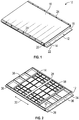
FIG. 1 is a perspective view of an embodiment of an electronic component assembly module; -
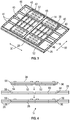
FIG. 2 is an illustration of an embodiment of a stiffener assembly of an assembly module; -
FIG. 3 is another illustration of an embodiment of a stiffener assembly of an assembly module; -
FIG. 4 is an illustration of a process of assembly of an embodiment of a stiffener assembly; -
FIG. 5 is an illustration of a process of assembly of an embodiment of an assembly module; and -
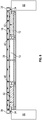
FIG. 6 is an illustration of thermal energy conduction in an embodiment of an assembly module. - A detailed description of one or more embodiments of the disclosed apparatus and method are presented herein by way of exemplification and not limitation with reference to the Figures.
- Referring now to
FIG. 1 , shown is a perspective view of an electroniccomponent assembly module 10. Theassembly module 10 includes a printed wiring board (PWB) 12, andstiffener assembly 14 secured to thePWB 12, afirst cover 16 disposed at afirst side 18 of thePWB 12 over thestiffener assembly 14, and asecond cover 20 disposed at asecond side 22 of thePWB 12 opposite thefirst side 18.Wedge locks 24, or other securing mechanism are utilized to secure theassembly module 10 into its completed form in an electronic box. - Referring now to
FIGs. 2 and3 , shown are partially disassembled views of theassembly module 10.FIG. 2 illustrates thestiffener assembly 14 assembled to thePWB 12. Thestiffener assembly 14 includes anouter stiffener 26 and aninner stiffener 28 installed into theouter stiffener 26. Theouter stiffener 26 and theinner stiffener 28 are formed from highly thermally conductive materials, such as aluminum or an aluminum alloy. As shown, theinner stiffener 28 is located inside theouter stiffener 26 in alengthwise direction 30 of thestiffener assembly 14. Thestiffener assembly 14 includes abottom side 32 and atop side 34 opposite thebottom side 32, with the anouter stiffener portion 36 of thebottom side 32 bonded to thePWB 12 by, for example, an adhesive material between theouter stiffener portion 36 and thePWB 12. Theinner stiffener 28 is not in bonded contact with thePWB 12 and is easily removable from theouter stiffener 26 and from thePWB 12. Theinner stiffener 28 is secured to theouter stiffener 26 via thewedge locks 24. Theinner stiffener 28 and theouter stiffener 26 includewedge lock rails 38 extending in thelengthwise direction 30 onto which thewedge locks 24 are installed. - Referring now to
FIG. 3 , shown is a view of thestiffener assembly 14 removed from thePWB 12, with thefirst cover 16 installed to thetop side 34 of thestiffener assembly 14. As can be seen inFIG. 3 thestiffener assembly 14 includes a plurality ofinner stiffener ribs 40 in theinner stiffener 28, which define a plurality ofinner stiffener pockets 42 therebetween. Similarly, theouter stiffener 26 includes a plurality ofouter stiffener ribs 44 defining a plurality ofouter stiffener pockets 46 therebetween. Theinner stiffener 28 may include acenter rail 48 extending across theinner stiffener 28 in awidthwise direction 50 perpendicular to the lengthwise direction. In some embodiments, theinner stiffener 28 is symmetrical about thecenter rail 48. Further, in some embodiments, thecenter rail 48 has a larger cross-sectional area than theinner stiffener ribs 40. - One or more electronic components are installed in the plurality of inner stiffener pockets 42 such that when the
assembly module 10 is completed, the one or more electronic components are electrically connected to thePWB 12. For example, in the embodiment ofFIG. 3 , the electronic components are four half-bridge modules 52. Thehalf bridge modules 52 are each secured in aninner stiffener pocket 42 with, for example one or more screws or other fasteners. While four half-bridge modules 52 are shown installed to the inner stiffener pockets 42, one skilled in the design of a printed wiring board will readily appreciate that additional electronic components, and/or components other than half-bridge assemblies 52 may be installed to the inner stiffener pockets 42. Examples of such other electronic components include MOSFETs, diodes, transistors or the like. - The
assembly module 10 is configured for ease of assembly of thehalf bridge modules 52 into theassembly module 10 and also ease of replacement of thehalf bridge modules 52 via installation and removal of theinner stiffener 28. To assemble theassembly module 10, referring toFIG. 4 , thehalf bridge modules 52 are installed at an inner stiffenerbottom side 54. Theinner stiffener 28 is then installed to theouter stiffener 26. Theinner stiffener 28 includes a tapered innerstiffener end 56, and theouter stiffener 26 includes a complimentary tapered outerstiffener end 58. The tapered outerstiffener end 58 defines an opening 62 into which theinner stiffener 28 is installed, with the tapered outerstiffener end 58 and the tapered innerstiffener end 56 acting as a guide for alignment and installation of theinner stiffener 28 into theouter stiffener 26. - Referring now to
FIG. 5 , after theinner stiffener 28 is installed to theouter stiffener 26 to form thestiffener assembly 14, thestiffener assembly 14 is installed to thePWB 12, with theouter stiffener 26 secured to thePWB 12 via an adhesive to define a bonded, inseparable joint between thePWB 12 and theouter stiffener 26. Eachhalf bridge module 52 is electrically connected to thePWB 12 via a plurality of fasteners. Thefirst cover 16 and thesecond cover 20 are then installed to thestiffener assembly 14 andPWB 12. Wedge locks 24 are installed at the wedge lock rails 38 to complete theassembly module 10. - Referring now to
FIG. 6 , illustrated is a cross-sectional view of theassembly module 10 illustrating the conduction heat transfer in theassembly module 10 to dissipate thermal energy from thehalf bridge modules 52. Thehalf bridge modules 52 generate heat during operation, and the heat is conducted in the upward direction from thehalf bridge modules 52 into theinner stiffener 28. From thehalf bridge modules 52, the thermal energy is conducted into theinner stiffener 28 and into theouter stiffener 26 via, for example, theinner stiffener ribs 40 and into theouter stiffener 26 via theouter stiffener ribs 44. The thermal energy is conducted toward and into the wedge lock rails 38, where the thermal energy is removed from theassembly module 10 via aheat removal device 60 such as, for example, a cold plate or a fan. Additionally, a small part of the thermal energy from the half bridge modules is conducted through thefirst cover 16 toward the wedge lock rails 38 for additional heat removal capability from thehalf bridge modules 52. - The
assembly module 10 andstiffener assembly 14 described herein provides a unique thermal management solution for thehalf bridge modules 52. Further, the structure provides for improved ease of assembly and improved ease of disassembly of thehalf bridge modules 52 in theassembly module 10, thus improving ease of repair and/or replacement of thehalf bridge modules 52. Further, theassembly module 10 may be utilized in a myriad of applications, such as deep space, ground-based or underwater-based applications. - The term "about" is intended to include the degree of error associated with measurement of the particular quantity based upon the equipment available at the time of filing the application.
- The terminology used herein is for the purpose of describing particular embodiments only and is not intended to be limiting of the present disclosure. As used herein, the singular forms "a", "an" and "the" are intended to include the plural forms as well, unless the context clearly indicates otherwise. It will be further understood that the terms "comprises" and/or "comprising," when used in this specification, specify the presence of stated features, integers, steps, operations, elements, and/or components, but do not preclude the presence or addition of one or more other features, integers, steps, operations, element components, and/or groups thereof.
- While the present disclosure has been described with reference to an exemplary embodiment or embodiments, it will be understood by those skilled in the art that various changes may be made and equivalents may be substituted for elements thereof without departing from the scope of the present disclosure. In addition, many modifications may be made to adapt a particular situation or material to the teachings of the present disclosure without departing from the essential scope thereof. Therefore, it is intended that the present disclosure not be limited to the particular embodiment disclosed as the best mode contemplated for carrying out this present disclosure, but that the present disclosure will include all embodiments falling within the scope of the claims.
Claims (14)
Applications Claiming Priority (1)
| Application Number | Priority Date | Filing Date | Title |
|---|---|---|---|
| US16/810,342 US11259445B2 (en) | 2020-03-05 | 2020-03-05 | Cooling mechanism for electrionic component mounted on a printed wiring board |
Publications (2)
| Publication Number | Publication Date |
|---|---|
| EP3893613A1 true EP3893613A1 (en) | 2021-10-13 |
| EP3893613B1 EP3893613B1 (en) | 2024-02-21 |
Family
ID=74856635
Family Applications (1)
| Application Number | Title | Priority Date | Filing Date |
|---|---|---|---|
| EP21160244.6A Active EP3893613B1 (en) | 2020-03-05 | 2021-03-02 | Cooling mechanism for electrionic component mounted on a printed wiring board |
Country Status (3)
| Country | Link |
|---|---|
| US (1) | US11259445B2 (en) |
| EP (1) | EP3893613B1 (en) |
| JP (1) | JP7633041B2 (en) |
Citations (3)
| Publication number | Priority date | Publication date | Assignee | Title |
|---|---|---|---|---|
| US7381908B1 (en) * | 2005-07-07 | 2008-06-03 | Cosimo Cantatore | Circuit board stiffener |
| US20140048326A1 (en) * | 2012-08-14 | 2014-02-20 | Bridge Semiconductor Corporation | Multi-cavity wiring board for semiconductor assembly with internal electromagnetic shielding |
| US20190115269A1 (en) * | 2017-03-08 | 2019-04-18 | Mediatek Inc. | Semiconductor package having a stiffener ring |
Family Cites Families (26)
| Publication number | Priority date | Publication date | Assignee | Title |
|---|---|---|---|---|
| DE2443122B2 (en) * | 1974-09-09 | 1979-05-17 | Siemens Ag, 1000 Berlin Und 8000 Muenchen | Device for high frequency and communications engineering |
| US5003429A (en) * | 1990-07-09 | 1991-03-26 | International Business Machines Corporation | Electronic assembly with enhanced heat sinking |
| US5339221A (en) * | 1992-07-31 | 1994-08-16 | Hughes Aircraft Company | Printed circuit board mounting cage |
| IL130775A (en) | 1999-07-02 | 2007-03-08 | Elta Systems Ltd | Conduction cooled electronic card module and method of producing the same utilizing an electronic circuit card originally designed for convection cooling |
| US6285556B1 (en) | 1999-08-05 | 2001-09-04 | Eaton Corporation | Electrical board securement and voltage isolation device |
| US6239972B1 (en) | 1999-12-13 | 2001-05-29 | Honeywell International Inc. | Integrated convection and conduction heat sink for multiple mounting positions |
| FR2809281B1 (en) | 2000-05-22 | 2002-07-12 | Alstom | ELECTRONIC POWER DEVICE |
| US6634095B2 (en) * | 2001-06-27 | 2003-10-21 | International Business Machines Corporation | Apparatus for mounting a land grid array module |
| US6760220B2 (en) * | 2002-11-25 | 2004-07-06 | Lockheed Martin Corporation | Rugged modular PC 104 chassis with blind mate connector and forced convection cooling capabilities |
| US20060109631A1 (en) | 2004-11-02 | 2006-05-25 | Data Device Corporation | Method and apparatus for connecting circuit cards employing a cooling technique to achieve desired temperature thresholds and card alignment |
| US7180737B2 (en) * | 2004-12-20 | 2007-02-20 | Harris Corporation | Heat exchanger system for circuit card assemblies |
| US8223494B2 (en) | 2007-12-31 | 2012-07-17 | General Electric Company | Conduction cooled circuit board assembly |
| US8009420B1 (en) | 2008-09-30 | 2011-08-30 | Lockheed Martin Corporation | Heat transfer of processing systems |
| US8942005B2 (en) | 2009-05-21 | 2015-01-27 | Raytheon Company | Low cost, high strength electronics module for airborne object |
| ITMI20111213A1 (en) | 2011-06-30 | 2012-12-31 | St Microelectronics Srl | SEMI-BRIDGE ELECTRONIC DEVICE WITH COMMON AUXILIARY HEAT SINK |
| US8987777B2 (en) | 2011-07-11 | 2015-03-24 | International Rectifier Corporation | Stacked half-bridge power module |
| JP2014175188A (en) | 2013-03-08 | 2014-09-22 | Funai Electric Co Ltd | Lighting device |
| CN203746840U (en) | 2014-01-24 | 2014-07-30 | 嘉兴斯达微电子有限公司 | High-power half-bridge module |
| JP2017054988A (en) | 2015-09-10 | 2017-03-16 | 日本精工株式会社 | Electronic component mounting board |
| FR3047869B1 (en) | 2016-02-11 | 2019-08-16 | Alstom Transport Technologies | DEVICE FOR SUPPORTING AT LEAST TWO ELECTRONIC CARDS, ELECTRONIC MODULE AND ELECTRONIC SYSTEM THEREOF |
| US9781867B2 (en) | 2016-02-19 | 2017-10-03 | Ford Global Technologies, Llc | Power module assembly for a vehicle power inverter |
| KR101841836B1 (en) | 2016-07-05 | 2018-03-26 | 김구용 | PCB module having multi-directional heat-radiation structure, and radiation plate, multi-layer PCB assembly, and module case used in the same PCB module |
| US10791652B2 (en) | 2018-06-12 | 2020-09-29 | Eagle Technology, Llc | Systems and methods for heatsink to rail thermal interface enhancement |
| CN110254247A (en) | 2019-06-18 | 2019-09-20 | 深圳市麦格米特驱动技术有限公司 | A kind of half-bridge power module component, electric machine controller (PCC) power and electric car |
| CN110266193B (en) | 2019-06-28 | 2020-05-22 | 西安交通大学 | Structure suitable for high-power boost LLC resonant converter |
| CN110601615A (en) | 2019-09-26 | 2019-12-20 | 黄山学院 | Direct current motor driving device with good heat dissipation |
-
2020
- 2020-03-05 US US16/810,342 patent/US11259445B2/en active Active
-
2021
- 2021-03-02 EP EP21160244.6A patent/EP3893613B1/en active Active
- 2021-03-03 JP JP2021033104A patent/JP7633041B2/en active Active
Patent Citations (3)
| Publication number | Priority date | Publication date | Assignee | Title |
|---|---|---|---|---|
| US7381908B1 (en) * | 2005-07-07 | 2008-06-03 | Cosimo Cantatore | Circuit board stiffener |
| US20140048326A1 (en) * | 2012-08-14 | 2014-02-20 | Bridge Semiconductor Corporation | Multi-cavity wiring board for semiconductor assembly with internal electromagnetic shielding |
| US20190115269A1 (en) * | 2017-03-08 | 2019-04-18 | Mediatek Inc. | Semiconductor package having a stiffener ring |
Also Published As
| Publication number | Publication date |
|---|---|
| US11259445B2 (en) | 2022-02-22 |
| JP2021141324A (en) | 2021-09-16 |
| EP3893613B1 (en) | 2024-02-21 |
| US20210282299A1 (en) | 2021-09-09 |
| JP7633041B2 (en) | 2025-02-19 |
Similar Documents
| Publication | Publication Date | Title |
|---|---|---|
| US6873528B2 (en) | Supplemental heat conduction path for card to chassis heat dissipation | |
| US20170273218A1 (en) | Electronic device and method of assembling such a device | |
| US6151215A (en) | Single mount and cooling for two two-sided printed circuit boards | |
| US6970358B2 (en) | Stack up assembly | |
| US5305185A (en) | Coplanar heatsink and electronics assembly | |
| US6832410B2 (en) | High performance cooling device with side mount fan | |
| EP1770774A2 (en) | Heatsink Assembly | |
| EP3557964B1 (en) | Electronics cooling module | |
| CN100579349C (en) | Support assemblies for printed circuit boards | |
| US10522442B2 (en) | Dissipating heat from an electronic device in a protective housing | |
| US9648789B2 (en) | Apparatus for cooling and mounting a circuit board | |
| US11259445B2 (en) | Cooling mechanism for electrionic component mounted on a printed wiring board | |
| US20220359342A1 (en) | Securing power semiconductor components to curved surfaces | |
| EP3882963B1 (en) | Conductive thermal management architecture employing a stiffener of a printed wiring board assembly | |
| EP3206470A1 (en) | Frame for holding an electronic board, housing, and rack including frame and housing | |
| US11140767B2 (en) | Conductive thermal management architecture for electronic modules in a two-card assembly | |
| EP3996480B1 (en) | Conductive thermal management architecture for electronic devices | |
| US20180347915A1 (en) | Heat dissipation apparatus and assembly method for heat dissipation apparatus | |
| CN117204129A (en) | Cooling device for cooling semiconductor modules and converter with cooling device | |
| US12557231B2 (en) | Two-piece separable wedge clamp for thermal mechanical interface | |
| SU1051750A1 (en) | Radioelectronic unit | |
| SU1630000A1 (en) | RADIO ELECTRONIC UNIT | |
| CN116017930A (en) | Sealing of thermal interface materials for power electronics modules |
Legal Events
| Date | Code | Title | Description |
|---|---|---|---|
| PUAI | Public reference made under article 153(3) epc to a published international application that has entered the european phase |
Free format text: ORIGINAL CODE: 0009012 |
|
| STAA | Information on the status of an ep patent application or granted ep patent |
Free format text: STATUS: THE APPLICATION HAS BEEN PUBLISHED |
|
| AK | Designated contracting states |
Kind code of ref document: A1 Designated state(s): AL AT BE BG CH CY CZ DE DK EE ES FI FR GB GR HR HU IE IS IT LI LT LU LV MC MK MT NL NO PL PT RO RS SE SI SK SM TR |
|
| STAA | Information on the status of an ep patent application or granted ep patent |
Free format text: STATUS: REQUEST FOR EXAMINATION WAS MADE |
|
| 17P | Request for examination filed |
Effective date: 20220408 |
|
| RBV | Designated contracting states (corrected) |
Designated state(s): AL AT BE BG CH CY CZ DE DK EE ES FI FR GB GR HR HU IE IS IT LI LT LU LV MC MK MT NL NO PL PT RO RS SE SI SK SM TR |
|
| GRAP | Despatch of communication of intention to grant a patent |
Free format text: ORIGINAL CODE: EPIDOSNIGR1 |
|
| STAA | Information on the status of an ep patent application or granted ep patent |
Free format text: STATUS: GRANT OF PATENT IS INTENDED |
|
| INTG | Intention to grant announced |
Effective date: 20230913 |
|
| GRAS | Grant fee paid |
Free format text: ORIGINAL CODE: EPIDOSNIGR3 |
|
| GRAA | (expected) grant |
Free format text: ORIGINAL CODE: 0009210 |
|
| STAA | Information on the status of an ep patent application or granted ep patent |
Free format text: STATUS: THE PATENT HAS BEEN GRANTED |
|
| AK | Designated contracting states |
Kind code of ref document: B1 Designated state(s): AL AT BE BG CH CY CZ DE DK EE ES FI FR GB GR HR HU IE IS IT LI LT LU LV MC MK MT NL NO PL PT RO RS SE SI SK SM TR |
|
| REG | Reference to a national code |
Ref country code: GB Ref legal event code: FG4D |
|
| REG | Reference to a national code |
Ref country code: CH Ref legal event code: EP |
|
| REG | Reference to a national code |
Ref country code: IE Ref legal event code: FG4D |
|
| REG | Reference to a national code |
Ref country code: DE Ref legal event code: R096 Ref document number: 602021009478 Country of ref document: DE |
|
| REG | Reference to a national code |
Ref country code: LT Ref legal event code: MG9D |
|
| REG | Reference to a national code |
Ref country code: NL Ref legal event code: MP Effective date: 20240221 |
|
| PG25 | Lapsed in a contracting state [announced via postgrant information from national office to epo] |
Ref country code: IS Free format text: LAPSE BECAUSE OF FAILURE TO SUBMIT A TRANSLATION OF THE DESCRIPTION OR TO PAY THE FEE WITHIN THE PRESCRIBED TIME-LIMIT Effective date: 20240621 |
|
| PG25 | Lapsed in a contracting state [announced via postgrant information from national office to epo] |
Ref country code: LT Free format text: LAPSE BECAUSE OF FAILURE TO SUBMIT A TRANSLATION OF THE DESCRIPTION OR TO PAY THE FEE WITHIN THE PRESCRIBED TIME-LIMIT Effective date: 20240221 |
|
| PG25 | Lapsed in a contracting state [announced via postgrant information from national office to epo] |
Ref country code: GR Free format text: LAPSE BECAUSE OF FAILURE TO SUBMIT A TRANSLATION OF THE DESCRIPTION OR TO PAY THE FEE WITHIN THE PRESCRIBED TIME-LIMIT Effective date: 20240522 |
|
| REG | Reference to a national code |
Ref country code: AT Ref legal event code: MK05 Ref document number: 1660248 Country of ref document: AT Kind code of ref document: T Effective date: 20240221 |
|
| PG25 | Lapsed in a contracting state [announced via postgrant information from national office to epo] |
Ref country code: NL Free format text: LAPSE BECAUSE OF FAILURE TO SUBMIT A TRANSLATION OF THE DESCRIPTION OR TO PAY THE FEE WITHIN THE PRESCRIBED TIME-LIMIT Effective date: 20240221 Ref country code: HR Free format text: LAPSE BECAUSE OF FAILURE TO SUBMIT A TRANSLATION OF THE DESCRIPTION OR TO PAY THE FEE WITHIN THE PRESCRIBED TIME-LIMIT Effective date: 20240221 Ref country code: RS Free format text: LAPSE BECAUSE OF FAILURE TO SUBMIT A TRANSLATION OF THE DESCRIPTION OR TO PAY THE FEE WITHIN THE PRESCRIBED TIME-LIMIT Effective date: 20240521 |
|
| PG25 | Lapsed in a contracting state [announced via postgrant information from national office to epo] |
Ref country code: ES Free format text: LAPSE BECAUSE OF FAILURE TO SUBMIT A TRANSLATION OF THE DESCRIPTION OR TO PAY THE FEE WITHIN THE PRESCRIBED TIME-LIMIT Effective date: 20240221 |
|
| PG25 | Lapsed in a contracting state [announced via postgrant information from national office to epo] |
Ref country code: AT Free format text: LAPSE BECAUSE OF FAILURE TO SUBMIT A TRANSLATION OF THE DESCRIPTION OR TO PAY THE FEE WITHIN THE PRESCRIBED TIME-LIMIT Effective date: 20240221 |
|
| PG25 | Lapsed in a contracting state [announced via postgrant information from national office to epo] |
Ref country code: RS Free format text: LAPSE BECAUSE OF FAILURE TO SUBMIT A TRANSLATION OF THE DESCRIPTION OR TO PAY THE FEE WITHIN THE PRESCRIBED TIME-LIMIT Effective date: 20240521 Ref country code: NO Free format text: LAPSE BECAUSE OF FAILURE TO SUBMIT A TRANSLATION OF THE DESCRIPTION OR TO PAY THE FEE WITHIN THE PRESCRIBED TIME-LIMIT Effective date: 20240521 Ref country code: NL Free format text: LAPSE BECAUSE OF FAILURE TO SUBMIT A TRANSLATION OF THE DESCRIPTION OR TO PAY THE FEE WITHIN THE PRESCRIBED TIME-LIMIT Effective date: 20240221 Ref country code: LT Free format text: LAPSE BECAUSE OF FAILURE TO SUBMIT A TRANSLATION OF THE DESCRIPTION OR TO PAY THE FEE WITHIN THE PRESCRIBED TIME-LIMIT Effective date: 20240221 Ref country code: IS Free format text: LAPSE BECAUSE OF FAILURE TO SUBMIT A TRANSLATION OF THE DESCRIPTION OR TO PAY THE FEE WITHIN THE PRESCRIBED TIME-LIMIT Effective date: 20240621 Ref country code: HR Free format text: LAPSE BECAUSE OF FAILURE TO SUBMIT A TRANSLATION OF THE DESCRIPTION OR TO PAY THE FEE WITHIN THE PRESCRIBED TIME-LIMIT Effective date: 20240221 Ref country code: GR Free format text: LAPSE BECAUSE OF FAILURE TO SUBMIT A TRANSLATION OF THE DESCRIPTION OR TO PAY THE FEE WITHIN THE PRESCRIBED TIME-LIMIT Effective date: 20240522 Ref country code: FI Free format text: LAPSE BECAUSE OF FAILURE TO SUBMIT A TRANSLATION OF THE DESCRIPTION OR TO PAY THE FEE WITHIN THE PRESCRIBED TIME-LIMIT Effective date: 20240221 Ref country code: ES Free format text: LAPSE BECAUSE OF FAILURE TO SUBMIT A TRANSLATION OF THE DESCRIPTION OR TO PAY THE FEE WITHIN THE PRESCRIBED TIME-LIMIT Effective date: 20240221 Ref country code: BG Free format text: LAPSE BECAUSE OF FAILURE TO SUBMIT A TRANSLATION OF THE DESCRIPTION OR TO PAY THE FEE WITHIN THE PRESCRIBED TIME-LIMIT Effective date: 20240221 Ref country code: AT Free format text: LAPSE BECAUSE OF FAILURE TO SUBMIT A TRANSLATION OF THE DESCRIPTION OR TO PAY THE FEE WITHIN THE PRESCRIBED TIME-LIMIT Effective date: 20240221 |
|
| PG25 | Lapsed in a contracting state [announced via postgrant information from national office to epo] |
Ref country code: PT Free format text: LAPSE BECAUSE OF FAILURE TO SUBMIT A TRANSLATION OF THE DESCRIPTION OR TO PAY THE FEE WITHIN THE PRESCRIBED TIME-LIMIT Effective date: 20240621 Ref country code: PL Free format text: LAPSE BECAUSE OF FAILURE TO SUBMIT A TRANSLATION OF THE DESCRIPTION OR TO PAY THE FEE WITHIN THE PRESCRIBED TIME-LIMIT Effective date: 20240221 |
|
| PG25 | Lapsed in a contracting state [announced via postgrant information from national office to epo] |
Ref country code: SE Free format text: LAPSE BECAUSE OF FAILURE TO SUBMIT A TRANSLATION OF THE DESCRIPTION OR TO PAY THE FEE WITHIN THE PRESCRIBED TIME-LIMIT Effective date: 20240221 Ref country code: PT Free format text: LAPSE BECAUSE OF FAILURE TO SUBMIT A TRANSLATION OF THE DESCRIPTION OR TO PAY THE FEE WITHIN THE PRESCRIBED TIME-LIMIT Effective date: 20240621 Ref country code: PL Free format text: LAPSE BECAUSE OF FAILURE TO SUBMIT A TRANSLATION OF THE DESCRIPTION OR TO PAY THE FEE WITHIN THE PRESCRIBED TIME-LIMIT Effective date: 20240221 Ref country code: LV Free format text: LAPSE BECAUSE OF FAILURE TO SUBMIT A TRANSLATION OF THE DESCRIPTION OR TO PAY THE FEE WITHIN THE PRESCRIBED TIME-LIMIT Effective date: 20240221 |
|
| PG25 | Lapsed in a contracting state [announced via postgrant information from national office to epo] |
Ref country code: DK Free format text: LAPSE BECAUSE OF FAILURE TO SUBMIT A TRANSLATION OF THE DESCRIPTION OR TO PAY THE FEE WITHIN THE PRESCRIBED TIME-LIMIT Effective date: 20240221 |
|
| PG25 | Lapsed in a contracting state [announced via postgrant information from national office to epo] |
Ref country code: SM Free format text: LAPSE BECAUSE OF FAILURE TO SUBMIT A TRANSLATION OF THE DESCRIPTION OR TO PAY THE FEE WITHIN THE PRESCRIBED TIME-LIMIT Effective date: 20240221 |
|
| PG25 | Lapsed in a contracting state [announced via postgrant information from national office to epo] |
Ref country code: EE Free format text: LAPSE BECAUSE OF FAILURE TO SUBMIT A TRANSLATION OF THE DESCRIPTION OR TO PAY THE FEE WITHIN THE PRESCRIBED TIME-LIMIT Effective date: 20240221 Ref country code: CZ Free format text: LAPSE BECAUSE OF FAILURE TO SUBMIT A TRANSLATION OF THE DESCRIPTION OR TO PAY THE FEE WITHIN THE PRESCRIBED TIME-LIMIT Effective date: 20240221 |
|
| PG25 | Lapsed in a contracting state [announced via postgrant information from national office to epo] |
Ref country code: SK Free format text: LAPSE BECAUSE OF FAILURE TO SUBMIT A TRANSLATION OF THE DESCRIPTION OR TO PAY THE FEE WITHIN THE PRESCRIBED TIME-LIMIT Effective date: 20240221 |
|
| PG25 | Lapsed in a contracting state [announced via postgrant information from national office to epo] |
Ref country code: SM Free format text: LAPSE BECAUSE OF FAILURE TO SUBMIT A TRANSLATION OF THE DESCRIPTION OR TO PAY THE FEE WITHIN THE PRESCRIBED TIME-LIMIT Effective date: 20240221 Ref country code: SK Free format text: LAPSE BECAUSE OF FAILURE TO SUBMIT A TRANSLATION OF THE DESCRIPTION OR TO PAY THE FEE WITHIN THE PRESCRIBED TIME-LIMIT Effective date: 20240221 Ref country code: RO Free format text: LAPSE BECAUSE OF FAILURE TO SUBMIT A TRANSLATION OF THE DESCRIPTION OR TO PAY THE FEE WITHIN THE PRESCRIBED TIME-LIMIT Effective date: 20240221 Ref country code: EE Free format text: LAPSE BECAUSE OF FAILURE TO SUBMIT A TRANSLATION OF THE DESCRIPTION OR TO PAY THE FEE WITHIN THE PRESCRIBED TIME-LIMIT Effective date: 20240221 Ref country code: DK Free format text: LAPSE BECAUSE OF FAILURE TO SUBMIT A TRANSLATION OF THE DESCRIPTION OR TO PAY THE FEE WITHIN THE PRESCRIBED TIME-LIMIT Effective date: 20240221 Ref country code: CZ Free format text: LAPSE BECAUSE OF FAILURE TO SUBMIT A TRANSLATION OF THE DESCRIPTION OR TO PAY THE FEE WITHIN THE PRESCRIBED TIME-LIMIT Effective date: 20240221 |
|
| REG | Reference to a national code |
Ref country code: CH Ref legal event code: PL |
|
| PG25 | Lapsed in a contracting state [announced via postgrant information from national office to epo] |
Ref country code: LU Free format text: LAPSE BECAUSE OF NON-PAYMENT OF DUE FEES Effective date: 20240302 |
|
| PG25 | Lapsed in a contracting state [announced via postgrant information from national office to epo] |
Ref country code: MC Free format text: LAPSE BECAUSE OF FAILURE TO SUBMIT A TRANSLATION OF THE DESCRIPTION OR TO PAY THE FEE WITHIN THE PRESCRIBED TIME-LIMIT Effective date: 20240221 |
|
| REG | Reference to a national code |
Ref country code: DE Ref legal event code: R097 Ref document number: 602021009478 Country of ref document: DE |
|
| PG25 | Lapsed in a contracting state [announced via postgrant information from national office to epo] |
Ref country code: MC Free format text: LAPSE BECAUSE OF FAILURE TO SUBMIT A TRANSLATION OF THE DESCRIPTION OR TO PAY THE FEE WITHIN THE PRESCRIBED TIME-LIMIT Effective date: 20240221 Ref country code: LU Free format text: LAPSE BECAUSE OF NON-PAYMENT OF DUE FEES Effective date: 20240302 |
|
| PG25 | Lapsed in a contracting state [announced via postgrant information from national office to epo] |
Ref country code: IT Free format text: LAPSE BECAUSE OF FAILURE TO SUBMIT A TRANSLATION OF THE DESCRIPTION OR TO PAY THE FEE WITHIN THE PRESCRIBED TIME-LIMIT Effective date: 20240221 |
|
| REG | Reference to a national code |
Ref country code: BE Ref legal event code: MM Effective date: 20240331 |
|
| PLBE | No opposition filed within time limit |
Free format text: ORIGINAL CODE: 0009261 |
|
| STAA | Information on the status of an ep patent application or granted ep patent |
Free format text: STATUS: NO OPPOSITION FILED WITHIN TIME LIMIT |
|
| PG25 | Lapsed in a contracting state [announced via postgrant information from national office to epo] |
Ref country code: IT Free format text: LAPSE BECAUSE OF FAILURE TO SUBMIT A TRANSLATION OF THE DESCRIPTION OR TO PAY THE FEE WITHIN THE PRESCRIBED TIME-LIMIT Effective date: 20240221 |
|
| PG25 | Lapsed in a contracting state [announced via postgrant information from national office to epo] |
Ref country code: BE Free format text: LAPSE BECAUSE OF NON-PAYMENT OF DUE FEES Effective date: 20240331 |
|
| PG25 | Lapsed in a contracting state [announced via postgrant information from national office to epo] |
Ref country code: IE Free format text: LAPSE BECAUSE OF NON-PAYMENT OF DUE FEES Effective date: 20240302 |
|
| 26N | No opposition filed |
Effective date: 20241122 |
|
| PG25 | Lapsed in a contracting state [announced via postgrant information from national office to epo] |
Ref country code: IE Free format text: LAPSE BECAUSE OF NON-PAYMENT OF DUE FEES Effective date: 20240302 Ref country code: BE Free format text: LAPSE BECAUSE OF NON-PAYMENT OF DUE FEES Effective date: 20240331 Ref country code: CH Free format text: LAPSE BECAUSE OF NON-PAYMENT OF DUE FEES Effective date: 20240331 |
|
| PG25 | Lapsed in a contracting state [announced via postgrant information from national office to epo] |
Ref country code: SI Free format text: LAPSE BECAUSE OF FAILURE TO SUBMIT A TRANSLATION OF THE DESCRIPTION OR TO PAY THE FEE WITHIN THE PRESCRIBED TIME-LIMIT Effective date: 20240221 |
|
| PG25 | Lapsed in a contracting state [announced via postgrant information from national office to epo] |
Ref country code: CY Free format text: LAPSE BECAUSE OF FAILURE TO SUBMIT A TRANSLATION OF THE DESCRIPTION OR TO PAY THE FEE WITHIN THE PRESCRIBED TIME-LIMIT; INVALID AB INITIO Effective date: 20210302 |
|
| PG25 | Lapsed in a contracting state [announced via postgrant information from national office to epo] |
Ref country code: HU Free format text: LAPSE BECAUSE OF FAILURE TO SUBMIT A TRANSLATION OF THE DESCRIPTION OR TO PAY THE FEE WITHIN THE PRESCRIBED TIME-LIMIT; INVALID AB INITIO Effective date: 20210302 |
|
| PG25 | Lapsed in a contracting state [announced via postgrant information from national office to epo] |
Ref country code: TR Free format text: LAPSE BECAUSE OF FAILURE TO SUBMIT A TRANSLATION OF THE DESCRIPTION OR TO PAY THE FEE WITHIN THE PRESCRIBED TIME-LIMIT Effective date: 20240221 |
|
| PGFP | Annual fee paid to national office [announced via postgrant information from national office to epo] |
Ref country code: GB Payment date: 20260220 Year of fee payment: 6 |
|
| PGFP | Annual fee paid to national office [announced via postgrant information from national office to epo] |
Ref country code: DE Payment date: 20260219 Year of fee payment: 6 |
|
| PGFP | Annual fee paid to national office [announced via postgrant information from national office to epo] |
Ref country code: FR Payment date: 20260220 Year of fee payment: 6 |