EP3893389A1 - Inductor-capacitor oscillator with embedded second harmonic filter and associated dual core oscillator - Google Patents
Inductor-capacitor oscillator with embedded second harmonic filter and associated dual core oscillator Download PDFInfo
- Publication number
- EP3893389A1 EP3893389A1 EP20216423.2A EP20216423A EP3893389A1 EP 3893389 A1 EP3893389 A1 EP 3893389A1 EP 20216423 A EP20216423 A EP 20216423A EP 3893389 A1 EP3893389 A1 EP 3893389A1
- Authority
- EP
- European Patent Office
- Prior art keywords
- inductor
- oscillator
- transistor
- coupled
- capacitor
- Prior art date
- Legal status (The legal status is an assumption and is not a legal conclusion. Google has not performed a legal analysis and makes no representation as to the accuracy of the status listed.)
- Granted
Links
Images




Classifications
-
- H—ELECTRICITY
- H03—ELECTRONIC CIRCUITRY
- H03B—GENERATION OF OSCILLATIONS, DIRECTLY OR BY FREQUENCY-CHANGING, BY CIRCUITS EMPLOYING ACTIVE ELEMENTS WHICH OPERATE IN A NON-SWITCHING MANNER; GENERATION OF NOISE BY SUCH CIRCUITS
- H03B5/00—Generation of oscillations using amplifier with regenerative feedback from output to input
- H03B5/08—Generation of oscillations using amplifier with regenerative feedback from output to input with frequency-determining element comprising lumped inductance and capacitance
- H03B5/12—Generation of oscillations using amplifier with regenerative feedback from output to input with frequency-determining element comprising lumped inductance and capacitance active element in amplifier being semiconductor device
- H03B5/1206—Generation of oscillations using amplifier with regenerative feedback from output to input with frequency-determining element comprising lumped inductance and capacitance active element in amplifier being semiconductor device using multiple transistors for amplification
- H03B5/1212—Generation of oscillations using amplifier with regenerative feedback from output to input with frequency-determining element comprising lumped inductance and capacitance active element in amplifier being semiconductor device using multiple transistors for amplification the amplifier comprising a pair of transistors, wherein an output terminal of each being connected to an input terminal of the other, e.g. a cross coupled pair
-
- H—ELECTRICITY
- H03—ELECTRONIC CIRCUITRY
- H03B—GENERATION OF OSCILLATIONS, DIRECTLY OR BY FREQUENCY-CHANGING, BY CIRCUITS EMPLOYING ACTIVE ELEMENTS WHICH OPERATE IN A NON-SWITCHING MANNER; GENERATION OF NOISE BY SUCH CIRCUITS
- H03B5/00—Generation of oscillations using amplifier with regenerative feedback from output to input
- H03B5/08—Generation of oscillations using amplifier with regenerative feedback from output to input with frequency-determining element comprising lumped inductance and capacitance
- H03B5/12—Generation of oscillations using amplifier with regenerative feedback from output to input with frequency-determining element comprising lumped inductance and capacitance active element in amplifier being semiconductor device
- H03B5/1228—Generation of oscillations using amplifier with regenerative feedback from output to input with frequency-determining element comprising lumped inductance and capacitance active element in amplifier being semiconductor device the amplifier comprising one or more field effect transistors
-
- H—ELECTRICITY
- H03—ELECTRONIC CIRCUITRY
- H03B—GENERATION OF OSCILLATIONS, DIRECTLY OR BY FREQUENCY-CHANGING, BY CIRCUITS EMPLOYING ACTIVE ELEMENTS WHICH OPERATE IN A NON-SWITCHING MANNER; GENERATION OF NOISE BY SUCH CIRCUITS
- H03B5/00—Generation of oscillations using amplifier with regenerative feedback from output to input
- H03B5/02—Details
- H03B5/04—Modifications of generator to compensate for variations in physical values, e.g. power supply, load, temperature
-
- H—ELECTRICITY
- H03—ELECTRONIC CIRCUITRY
- H03B—GENERATION OF OSCILLATIONS, DIRECTLY OR BY FREQUENCY-CHANGING, BY CIRCUITS EMPLOYING ACTIVE ELEMENTS WHICH OPERATE IN A NON-SWITCHING MANNER; GENERATION OF NOISE BY SUCH CIRCUITS
- H03B1/00—Details
- H03B1/04—Reducing undesired oscillations, e.g. harmonics
-
- H—ELECTRICITY
- H03—ELECTRONIC CIRCUITRY
- H03B—GENERATION OF OSCILLATIONS, DIRECTLY OR BY FREQUENCY-CHANGING, BY CIRCUITS EMPLOYING ACTIVE ELEMENTS WHICH OPERATE IN A NON-SWITCHING MANNER; GENERATION OF NOISE BY SUCH CIRCUITS
- H03B2200/00—Indexing scheme relating to details of oscillators covered by H03B
- H03B2200/006—Functional aspects of oscillators
- H03B2200/007—Generation of oscillations based on harmonic frequencies, e.g. overtone oscillators
-
- H—ELECTRICITY
- H03—ELECTRONIC CIRCUITRY
- H03B—GENERATION OF OSCILLATIONS, DIRECTLY OR BY FREQUENCY-CHANGING, BY CIRCUITS EMPLOYING ACTIVE ELEMENTS WHICH OPERATE IN A NON-SWITCHING MANNER; GENERATION OF NOISE BY SUCH CIRCUITS
- H03B2200/00—Indexing scheme relating to details of oscillators covered by H03B
- H03B2200/006—Functional aspects of oscillators
- H03B2200/0076—Power combination of several oscillators oscillating at the same frequency
-
- H—ELECTRICITY
- H03—ELECTRONIC CIRCUITRY
- H03B—GENERATION OF OSCILLATIONS, DIRECTLY OR BY FREQUENCY-CHANGING, BY CIRCUITS EMPLOYING ACTIVE ELEMENTS WHICH OPERATE IN A NON-SWITCHING MANNER; GENERATION OF NOISE BY SUCH CIRCUITS
- H03B2200/00—Indexing scheme relating to details of oscillators covered by H03B
- H03B2200/006—Functional aspects of oscillators
- H03B2200/0088—Reduction of noise
- H03B2200/009—Reduction of phase noise
-
- H—ELECTRICITY
- H03—ELECTRONIC CIRCUITRY
- H03B—GENERATION OF OSCILLATIONS, DIRECTLY OR BY FREQUENCY-CHANGING, BY CIRCUITS EMPLOYING ACTIVE ELEMENTS WHICH OPERATE IN A NON-SWITCHING MANNER; GENERATION OF NOISE BY SUCH CIRCUITS
- H03B2202/00—Aspects of oscillators relating to reduction of undesired oscillations
- H03B2202/05—Reduction of undesired oscillations through filtering or through special resonator characteristics
Definitions
- the present invention is related to inductor-capacitor (LC) oscillator, and more particularly, to an LC oscillator with an embedded second harmonic filter and an associated dual core oscillator.
- LC inductor-capacitor
- an oscillator not only generates a fundamental frequency which is determined by a main resonant tank, but also generates unwanted second harmonic frequency which may cause noise up-conversion.
- An extra tank may be adapted to filter the second harmonic frequency in order to block or weaken the second harmonic frequency in related arts.
- An objective of the present invention is to provide an inductor-capacitor (LC) oscillator with an embedded second harmonic filter and an associated dual core oscillator, which have less sensitivity regarding the process variation and better noise-related performance (e.g. less phase noise) in comparison with the related arts.
- LC inductor-capacitor
- the LC oscillator may comprise a first transistor, a second transistor, a first part-one inductor, a second part-one inductor, a part-one capacitor, a part-two inductor and at least one part-two capacitor.
- a first end of the first part-one inductor and a first end of the second part-one inductor are coupled to gate terminals of the second transistor and the first transistor, respectively.
- the part-one capacitor is coupled between the first end of the first part-one inductor and the first end of the second part-one inductor.
- the part-two inductor is coupled between a second end of the first part-one inductor and a second end of the second part-one inductor.
- the at least one part-two capacitor is coupled to drain terminals of the first transistor and the second transistor.
- At least one embodiment of the present invention provides a dual core oscillator, wherein the dual core oscillator may comprise a first LC oscillator and a second LC oscillator identical to each other.
- Each of the first LC oscillator and the second LC oscillator may comprise a first transistor, a second transistor, a first part-one inductor, a second part-one inductor, a part-one capacitor, a part-two inductor and at least one part-two capacitor.
- a first end of the first part-one inductor and a first end of the second part-one inductor are coupled to gate terminals of the second transistor and the first transistor, respectively.
- the part-one capacitor is coupled between the first end of the first part-one inductor and the first end of the second part-one inductor.
- the part-two inductor is coupled between a second end of the first part-one inductor and a second end of the second part-one inductor.
- the at least one part-two capacitor is coupled to drain terminals of the first transistor and the second transistor. More particularly, the part-two inductor of the first LC oscillator is coupled to the part-two inductor of the second LC oscillator.
- the dual core oscillator may comprise an LC oscillator, wherein the LC oscillator may comprise a first transistor, a second transistor and a first LC tank.
- the first LC tank may comprise a first part-one inductor, a second part-one inductor, a part-one capacitor, a part-two inductor and at least one part-two capacitor.
- a first end of the first part-one inductor and a first end of the second part-one inductor are coupled to gate terminals of the second transistor and the first transistor, respectively.
- the part-one capacitor is coupled between the first end of the first part-one inductor and the first end of the second part-one inductor.
- the part-two inductor coupled between a second end of the first part-one inductor and a second end of the second part-one inductor.
- the at least one part-two capacitor coupled to drain terminals of the first transistor and the second transistor.
- the dual core oscillator may further comprise a second LC tank, which comprises at least one inductor and at least one capacitor. More particularly, the part-two inductor of the first LC oscillator is coupled to the at least one inductor of the second LC tank.
- the LC oscillator provided by embodiments of the present invention has an LC tank with an embedded second harmonic filter therein. All components (e.g. inductors and capacitors) within the LC tank can be laid out together, which greatly reduce sensitivity to the process variation in comparison with using a standalone second harmonic filter tank. In addition, embodiments of the present invention will not greatly increase overall costs. Thus, the present invention can solve the problem of the related art without introducing any side effect or in a way that is less likely to introduce side effects.
- FIG. 1A is a diagram illustrating an inductor-capacitor (LC) oscillator 10 with an embedded second harmonic filter according to an embodiment of the present invention.
- the LC oscillator 10 may comprise a first transistor such as a P-type transistor MP (e.g. P-type Metal-Oxide-Semiconductor Field-Effect Transistor (MOSFET)), a second transistor such as an N-type transistor MN (e.g.
- a P-type transistor MP e.g. P-type Metal-Oxide-Semiconductor Field-Effect Transistor (MOSFET)
- MOSFET Metal-Oxide-Semiconductor Field-Effect Transistor
- N-type MOSFET N-type MOSFET
- a first part-one inductor such as an inductor L 11
- a second part-one inductor such as an inductor L 12
- a part-one capacitor such as a capacitor C 1
- a part-two inductor such as an inductor L 2
- at least one part-two capacitor C 2 A first end of the inductor L 11 and a first end of the inductor L 12 are coupled to gate terminals of the N-type transistor MN and the P-type transistor MP, respectively.
- the capacitor C 1 is coupled between the first end of the inductor L 11 and the first end of the inductor L 12 .
- the inductor L 2 is coupled between a second end of the inductor L 11 and a second end of the inductor L 12 .
- the at least one part-two capacitor is coupled to drain terminals of the first transistor and the second transistor.
- the capacitor C 2 is coupled between the drain terminals of the P-type transistor MP and the N-type transistor MN.
- Source terminals of the P-type transistor MP and the N-type transistor MN are coupled to a supply voltage terminal (e.g. a terminal providing the highest fixed voltage level within the LC oscillator 10) and a ground voltage terminal (e.g. a terminal providing the lowest fixed voltage level within the LC oscillator 10), respectively.
- the LC oscillator 10 may further comprise a first part-three inductor such as an inductor L 31 and a second part-three inductor such as an inductor L 32 , where the inductor L 31 is coupled between the second end of the inductor L 11 and the drain terminal of the P-type transistor MP, and the inductor L 32 is coupled between the second end of the inductor L 12 and the drain terminal of the N-type transistor MN
- inductance and capacitance of corresponding components are indicated by italic of the same/similar symbols of the corresponding components.
- capacitance of the capacitor C 1 and capacitance of the capacitor C 2 are represented by C 1 and C 2 , respectively
- inductance of each of the inductors L 11 and L 12 is represented by L 1
- inductance of the inductor L2 is represented by L2
- inductance of each of the inductors L 31 and L 32 is represented by L 3 , where a symbol "s" may represent a variable associated with frequency and phase.
- at least the inductor L 2 , the capacitor C 2 , the inductors L 31 and L 32 constitute a second harmonic filter to block or weaken second harmonic signals of the LC oscillator 10.
- the inductors L 31 and L 32 may be omitted, e.g. the second end of inductor L 11 and the second end of the inductor L 12 may be directly connected to the drain terminals of the P-type transistor MP and the N-type transistor MN, respectively. Under this condition, at least the inductor L 2 and the capacitor C 2 constitute a second harmonic filter to block or weaken the second harmonic signals.
- the symbol ⁇ may represent a positive value, showing a larger C 2 multiplied by a factor for given 2fo, which is for illustrative purpose only, and is not meant to be a limitation of the present invention.
- a voltage gain Av from V 2 to V 1 is preferably as high as possible, where the voltage gain Av may be illustrated as follows:
- a V @ fo V 1
- V 2 1 + L 1 L 2 2 1 + s 2 L 3 2 C 2 1 + s 2 L 3 + L 2 2 2 C 2 ⁇ 1 + L 1 L 2
- the main purpose of the inductors L 31 and L 32 is to remove inevitable correlation between controlling the impedance Z in2 and controlling the voltage gain Av.
- the impedance Z in2 is desired to be as high as possible (more particularly, a peak resistance Rp of the impedance Z in2 is desired to be as high as possible) in order to block or weaken the second harmonic frequency 2fo.
- Q L Q C
- Q L Q C
- L 2 needs to be increased and C 2 needs to be reduced.
- the voltage gain Av will be decreasingly reached to unit.
- the LC oscillator 10 shown in FIG. 1A can effectively increase the impedance Z in2 at the second harmonic frequency 2 fo , and therefore improve the noise-related performance (e.g. less phase noise) and efficiency (e.g. figure of merit (FOM), which is related to power consumption, noise and signal swing).
- Another advantage of the LC oscillator 10 shown in FIG. 1A is that the second harmonic filter tracks variation caused by the fundamental frequency resonant tank. For example, when the capacitance C 1 varies and the resonant frequency of the fundamental frequency resonant tank is accordingly reduced (e.g. fo is reduced), the resonant frequency of the second harmonic filter will be reduced as well, substantially tracking the second harmonic frequency (e.g. tracking 2/0).
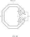
- the inductors L 11 , L 12 , L 2 , L 31 and L 32 can be laid out together, and more particularly, as shown in FIG. 1B , the inductors L 11 , L 12 , L 2 , L 31 and L 32 can be implemented by a continuous metal layer without segmentation. Even if the inductors L 31 and L 32 are omitted in some embodiments, the inductors L 11 , L 12 and L 2 also have the similar advantage of being implemented by a continuous metal layer without segmentation. Under this condition, impacts of process variation upon these components can be quite similar or substantially identical to each other, and mismatch (e.g. relative difference) between these components due to process variation can be minimized, which can minimize performance sensitivity to the process variation.
- mismatch e.g. relative difference
- FIG. 2 is a diagram illustrating an LC oscillator 20 according to an embodiment of the present invention.
- the LC oscillator 20 is quite similar to the LC oscillator 10 shown in FIG. 1A .
- the main difference is both of the first transistor and the second transistor are implemented by P-type transistors MP1 and MP2, the at least one capacitor is implemented by capacitors C 21 and C 22 , where the source terminal of the P-type transistors MP1 and MP2 are coupled to the supply voltage terminal, the capacitor C 21 is coupled between a drain terminal of the P-type transistor MP1 and the ground voltage terminal, the capacitor C 22 is coupled between a drain terminal of the P-type transistor MP2 and the ground voltage terminal, and a center tap of the inductor L 2 is coupled to the ground voltage terminal.
- the advantages and performance of the LC oscillator 20 are similar to that of the LC oscillator 10, and related details are not repeated here for brevity.
- FIG. 3 is a diagram illustrating an LC oscillator 30 according to an embodiment of the present invention.
- the LC oscillator 30 is quite similar to the LC oscillator 20 shown in FIG. 2 .
- the main difference is both of the first transistor and the second transistor are implemented by N-type transistors MN1 and MN2, where the source terminal of the N-type transistors MN1 and MN2 are coupled to the ground voltage terminal, the capacitor C 21 is coupled between a drain terminal of the N-type transistor MN1 and the supply voltage terminal, the capacitor C 22 is coupled between a drain terminal of the N-type transistor MN2 and the supply voltage terminal, and the center tap of the inductor L 2 is coupled to the supply voltage terminal.
- the advantages and performance of the LC oscillator 30 are similar to that of the LC oscillator 10, and related details are not repeated here for brevity.
- any additional filter can be further added on a path where the common mode current flows through, in order to build double second harmonic filtering.
- a tail filter can be added on a path where common mode current flow through in the LC oscillator 20 shown in FIG. 2 or the LC oscillator 30 shown in FIG. 3 .
- the tail filter e.g. an inductor L tail and a capacitor C tail connected in parallel
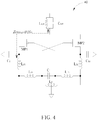
- the P-type transistors MP1 and MP2 can be coupled to source terminals of the P-type transistors MP1 and MP2, to configure an LC oscillator 40 as shown in FIG.
- an impedance Zcm high at the second harmonic frequency 2fo on a common mode signal path of the LC oscillator 40 are labeled "Zcm high@ 2fo" in FIG. 4 for brevity.
- the tail filter e.g. the inductor L tail and the capacitor C tail connected in parallel
- the impedance Zcm high at the second harmonic frequency 2fo on a common mode signal path of the LC oscillator 50 are labeled "Zcm high@ 2fo" in FIG. 5 for brevity.
- phase noise sensitivity of the LC oscillator 40 or 50 regarding capacitor variation can be greatly reduced.
- the configuration of adding the tail filter into the oscillator 30 may be deduced by analogy, and is therefore omitted here for brevity.
- FIG. 6A is a diagram illustrating a dual core oscillator 60 according to an embodiment of the present invention.
- the dual core oscillator may comprise a first LC oscillator and a second LC oscillator identical to each other.
- an upper half portion of the dual core oscillator 60 may be regarded as the first LC oscillator
- a lower half portion of the dual core oscillator 60 may be regarded as the second LC oscillator
- each of the first LC oscillator and the second LC oscillator may be implemented by the LC oscillator 10 shown in FIG. 1A , and the part-two inductor of the first LC oscillator is coupled to the part-two inductor of the second LC oscillator.
- the part-two inductor of the first LC oscillator and the part-two inductor of the second LC oscillator are implemented by inductors L 21 and L 22 , where a center tap of the inductor L 21 is coupled to a center tap of the inductor L 22 , and both of the inductors L 21 and L 22 have the inductance L 2 . More particularly, combination of an upper portion of the inductor L 21 and an upper portion of the inductor L 22 may be regarded as the part-two inductor of the first LC oscillator, and combination of a lower portion of the inductor L 21 and a lower portion of the inductor L 22 may be regarded as the part-two inductor of the second LC oscillator.
- all inductors e.g. the inductor L 11 /L 12 and the inductors L 31 /L 32 within both of the first LC oscillator and the second LC oscillator, and the inductors L 21 /L 22
- alternative designs of the LC oscillator 10 may be applied to the dual core oscillator 60, e.g. the inductors L 31 and L 32 within the first LC oscillator and the second LC oscillator of the dual core oscillator 60 may be omitted.
- all inductors e.g. the inductor L 11 /L 12 within both of the first LC oscillator and the second LC oscillator, and the inductors L 21 /L 22
- Design considerations of the dual core oscillator 60 with/without the inductors L 31 and L 32 may refer to the description related to the embodiment of FIG. 1A , and are not repeated here for brevity.
- the P-type transistor MP and the N-type transistor MN within the second LC oscillator shown in FIGs. 6A and 6B may be omitted.
- the second LC oscillator can be replaced with a second LC tank (e.g. without transistor therein), as shown by the lower half portion of a dual core oscillator 70 shown in FIG. 7A .
- the dual core oscillator 60 and the dual core oscillator 70 are whether to configure the P-type transistor MP and the N-type transistor MN in the second LC oscillator, other details of the dual core oscillator 70 are not repeated here for brevity.
- all inductors e.g.
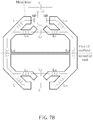
- the inductor L 11 /L 12 and the inductors L 31 /L 32 within both of the first LC oscillator and the second LC tank, and the inductors L 21 /L 22 ) can be implemented by a continuous metal layer without segmentation as shown in FIG. 7B .
- the dual core oscillators 60 and 70 are based on the architecture shown in FIG. 1A , the dual core oscillators 60 and 70 also have all the advantages of the LC oscillator 10. Furthermore, in comparison with utilizing a single LC oscillator (e.g. any of the LC oscillators 10, 20, 30, 40 and 50), the dual core oscillators 60 and 70 may effectively double output signal swing/power, and thereby equivalently reduce overall phase noise (e.g. improve 3dB) under a condition where the efficiency (e.g. FOM) is unchanged.
- overall phase noise e.g. improve 3dB
- the embodiments of the present invention provides an LC oscillator with an embedded second harmonic filter, which combines a fundamental resonant tank and a second harmonic filter into one LC network.
- the LC oscillator can effectively increase the impedance regarding second harmonic signals without sacrificing the voltage gain, and impact of process variation upon overall performance can be minimized, since capacitors and inductors mismatch can be minimized by properly layout as shown in the embodiments.
- the embodiments of the present invention will not greatly increase overall cost.
- the present invention can improve overall performance of the LC oscillator without introducing any side effect or in a way that is less likely to introduce side effects.
- the present invention may also be defined by means of the following numbered clauses.
Landscapes
- Inductance-Capacitance Distribution Constants And Capacitance-Resistance Oscillators (AREA)
Abstract
Description
- This application claims the benefit of
U.S. provisional application No. 63/006,810 - The present invention is related to inductor-capacitor (LC) oscillator, and more particularly, to an LC oscillator with an embedded second harmonic filter and an associated dual core oscillator.
- In general, an oscillator not only generates a fundamental frequency which is determined by a main resonant tank, but also generates unwanted second harmonic frequency which may cause noise up-conversion. An extra tank may be adapted to filter the second harmonic frequency in order to block or weaken the second harmonic frequency in related arts. Some disadvantages still exist in this architecture, however. For example, the main resonant tank and the extra tank may be independent and apart from each other, and process variation of components such as inductors and capacitors within the main resonant tank and the extra tank may degrade the performance of second harmonic filtering since their variations are typically also independent. Furthermore, the extra tank is usually designed to have low-quality factor (low-Q) because of the area limitation, and therefore has poor noise-related performance.
- Thus, there is a need for a novel architecture of an LC oscillator, which has less sensitivity regarding the process variation and better noise-related performance (e.g. less phase noise) in comparison with the related arts.
- An objective of the present invention is to provide an inductor-capacitor (LC) oscillator with an embedded second harmonic filter and an associated dual core oscillator, which have less sensitivity regarding the process variation and better noise-related performance (e.g. less phase noise) in comparison with the related arts.
- At least one embodiment of the present invention provides an LC oscillator with an embedded second harmonic filter. The LC oscillator may comprise a first transistor, a second transistor, a first part-one inductor, a second part-one inductor, a part-one capacitor, a part-two inductor and at least one part-two capacitor. A first end of the first part-one inductor and a first end of the second part-one inductor are coupled to gate terminals of the second transistor and the first transistor, respectively. The part-one capacitor is coupled between the first end of the first part-one inductor and the first end of the second part-one inductor. The part-two inductor is coupled between a second end of the first part-one inductor and a second end of the second part-one inductor. The at least one part-two capacitor is coupled to drain terminals of the first transistor and the second transistor.
- At least one embodiment of the present invention provides a dual core oscillator, wherein the dual core oscillator may comprise a first LC oscillator and a second LC oscillator identical to each other. Each of the first LC oscillator and the second LC oscillator may comprise a first transistor, a second transistor, a first part-one inductor, a second part-one inductor, a part-one capacitor, a part-two inductor and at least one part-two capacitor. A first end of the first part-one inductor and a first end of the second part-one inductor are coupled to gate terminals of the second transistor and the first transistor, respectively. The part-one capacitor is coupled between the first end of the first part-one inductor and the first end of the second part-one inductor. The part-two inductor is coupled between a second end of the first part-one inductor and a second end of the second part-one inductor. The at least one part-two capacitor is coupled to drain terminals of the first transistor and the second transistor. More particularly, the part-two inductor of the first LC oscillator is coupled to the part-two inductor of the second LC oscillator.
- At least one embodiment of the present invention provides a dual core oscillator. The dual core oscillator may comprise an LC oscillator, wherein the LC oscillator may comprise a first transistor, a second transistor and a first LC tank. The first LC tank may comprise a first part-one inductor, a second part-one inductor, a part-one capacitor, a part-two inductor and at least one part-two capacitor. A first end of the first part-one inductor and a first end of the second part-one inductor are coupled to gate terminals of the second transistor and the first transistor, respectively. The part-one capacitor is coupled between the first end of the first part-one inductor and the first end of the second part-one inductor. The part-two inductor, coupled between a second end of the first part-one inductor and a second end of the second part-one inductor. The at least one part-two capacitor, coupled to drain terminals of the first transistor and the second transistor. The dual core oscillator may further comprise a second LC tank, which comprises at least one inductor and at least one capacitor. More particularly, the part-two inductor of the first LC oscillator is coupled to the at least one inductor of the second LC tank.
- The LC oscillator provided by embodiments of the present invention has an LC tank with an embedded second harmonic filter therein. All components (e.g. inductors and capacitors) within the LC tank can be laid out together, which greatly reduce sensitivity to the process variation in comparison with using a standalone second harmonic filter tank. In addition, embodiments of the present invention will not greatly increase overall costs. Thus, the present invention can solve the problem of the related art without introducing any side effect or in a way that is less likely to introduce side effects.
- These and other objectives of the present invention will no doubt become obvious to those of ordinary skill in the art after reading the following detailed description of the preferred embodiment that is illustrated in the various figures and drawings.
-
-
FIG. 1A is a diagram illustrating an LC oscillator with an embedded second harmonic filter according to an embodiment of the present invention. -
FIG. 1B shows layout of inductors within the LC oscillator shown inFIG. 1A according to an embodiment of the present invention. -
FIG. 2 is a diagram illustrating an LC oscillator according to an embodiment of the present invention. -
FIG. 3 is a diagram illustrating an LC oscillator according to an embodiment of the present invention. -
FIG. 4 is a diagram illustrating an LC oscillator according to an embodiment of the present invention. -
FIG. 5 is a diagram illustrating an LC oscillator according to an embodiment of the present invention. -
FIG. 6A is a diagram illustrating a dual core oscillator according to an embodiment of the present invention. -
FIG. 6B shows layout of inductors within the dual core oscillator shown inFIG. 6A according to an embodiment of the present invention. -
FIG. 7A is a diagram illustrating a dual core oscillator according to another embodiment of the present invention. -
FIG. 7B shows layout of inductors within the dual core oscillator shown inFIG. 7A according to another embodiment of the present invention. - Certain terms are used throughout the following description and claims, which refer to particular components. As one skilled in the art will appreciate, electronic equipment manufacturers may refer to a component by different names. This document does not intend to distinguish between components that differ in name but not in function. In the following description and in the claims, the terms "include" and "comprise" are used in an open-ended fashion, and thus should be interpreted to mean "include, but not limited to ...". Also, the term "couple" is intended to mean either an indirect or direct electrical connection. Accordingly, if one device is coupled to another device, that connection may be through a direct electrical connection, or through an indirect electrical connection via other devices and connections.
-
FIG. 1A is a diagram illustrating an inductor-capacitor (LC)oscillator 10 with an embedded second harmonic filter according to an embodiment of the present invention. As shown inFIG. 1A , theLC oscillator 10 may comprise a first transistor such as a P-type transistor MP (e.g. P-type Metal-Oxide-Semiconductor Field-Effect Transistor (MOSFET)), a second transistor such as an N-type transistor MN (e.g. N-type MOSFET), a first part-one inductor such as an inductor L11, a second part-one inductor such as an inductor L12, a part-one capacitor such as a capacitor C1, a part-two inductor such as an inductor L2, and at least one part-two capacitor C2. A first end of the inductor L11 and a first end of the inductor L12 are coupled to gate terminals of the N-type transistor MN and the P-type transistor MP, respectively. The capacitor C1 is coupled between the first end of the inductor L11 and the first end of the inductor L12. The inductor L2 is coupled between a second end of the inductor L11 and a second end of the inductor L12. The at least one part-two capacitor is coupled to drain terminals of the first transistor and the second transistor. For example, the capacitor C2 is coupled between the drain terminals of the P-type transistor MP and the N-type transistor MN. Source terminals of the P-type transistor MP and the N-type transistor MN are coupled to a supply voltage terminal (e.g. a terminal providing the highest fixed voltage level within the LC oscillator 10) and a ground voltage terminal (e.g. a terminal providing the lowest fixed voltage level within the LC oscillator 10), respectively. - As shown in
FIG. 1A , theLC oscillator 10 may further comprise a first part-three inductor such as an inductor L31 and a second part-three inductor such as an inductor L32, where the inductor L31 is coupled between the second end of the inductor L11 and the drain terminal of the P-type transistor MP, and the inductor L32 is coupled between the second end of the inductor L12 and the drain terminal of the N-type transistor MN - For better illustration, inductance and capacitance of corresponding components are indicated by italic of the same/similar symbols of the corresponding components. For example, capacitance of the capacitor C1 and capacitance of the capacitor C2 are represented by C1 and C2, respectively, inductance of each of the inductors L11 and L12 is represented by L1 , inductance of the inductor L2 is represented by L2, inductance of each of the inductors L31 and L32 is represented by L3, where a symbol "s" may represent a variable associated with frequency and phase. As for the architecture which has the inductors L31 and L32 shown in
FIG. 1A , at least the inductors L11 and L12, the inductor L2 and the capacitor C1 constitute a fundamental frequency resonant tank. In detail, an impedance Zin1 at a fundamental frequency fo may be illustrated as follows:
LC oscillator 10. In detail, an impedance Zin2 at a second harmonic frequency 2fo may be illustrated as follows:
- In some embodiments, the inductors L31 and L32 may be omitted, e.g. the second end of inductor L11 and the second end of the inductor L12 may be directly connected to the drain terminals of the P-type transistor MP and the N-type transistor MN, respectively. Under this condition, at least the inductor L2 and the capacitor C2 constitute a second harmonic filter to block or weaken the second harmonic signals. In detail, the impedance Zin2 under the condition where the inductors L31 and L32 are omitted may be illustrated as follows:

- In general, a voltage gain Av from V2 to V1 is preferably as high as possible, where the voltage gain Av may be illustrated as follows:


LC oscillator 10. - In comparison with the related art, the
LC oscillator 10 shown inFIG. 1A can effectively increase the impedance Zin2 at the second harmonic frequency 2fo, and therefore improve the noise-related performance (e.g. less phase noise) and efficiency (e.g. figure of merit (FOM), which is related to power consumption, noise and signal swing). Another advantage of theLC oscillator 10 shown inFIG. 1A is that the second harmonic filter tracks variation caused by the fundamental frequency resonant tank. For example, when the capacitance C1 varies and the resonant frequency of the fundamental frequency resonant tank is accordingly reduced (e.g. fo is reduced), the resonant frequency of the second harmonic filter will be reduced as well, substantially tracking the second harmonic frequency (e.g. tracking 2/0). In addition, as both the fundamental frequency resonant tank and the second harmonic filter will not be separated by transistors (e.g. the P-type transistor MP and the N-type transistors MN), all of the inductors L11, L12, L2, L31 and L32 can be laid out together, and more particularly, as shown inFIG. 1B , the inductors L11, L12, L2, L31 and L32 can be implemented by a continuous metal layer without segmentation. Even if the inductors L31 and L32 are omitted in some embodiments, the inductors L11, L12 and L2 also have the similar advantage of being implemented by a continuous metal layer without segmentation. Under this condition, impacts of process variation upon these components can be quite similar or substantially identical to each other, and mismatch (e.g. relative difference) between these components due to process variation can be minimized, which can minimize performance sensitivity to the process variation. - It should be noted that the first transistor and the second transistor are not limited to utilizing different types of transistor.
FIG. 2 is a diagram illustrating anLC oscillator 20 according to an embodiment of the present invention. TheLC oscillator 20 is quite similar to theLC oscillator 10 shown inFIG. 1A . The main difference is both of the first transistor and the second transistor are implemented by P-type transistors MP1 and MP2, the at least one capacitor is implemented by capacitors C21 and C22, where the source terminal of the P-type transistors MP1 and MP2 are coupled to the supply voltage terminal, the capacitor C21 is coupled between a drain terminal of the P-type transistor MP1 and the ground voltage terminal, the capacitor C22 is coupled between a drain terminal of the P-type transistor MP2 and the ground voltage terminal, and a center tap of the inductor L2 is coupled to the ground voltage terminal. The advantages and performance of theLC oscillator 20 are similar to that of theLC oscillator 10, and related details are not repeated here for brevity. -
FIG. 3 is a diagram illustrating anLC oscillator 30 according to an embodiment of the present invention. TheLC oscillator 30 is quite similar to theLC oscillator 20 shown inFIG. 2 . The main difference is both of the first transistor and the second transistor are implemented by N-type transistors MN1 and MN2, where the source terminal of the N-type transistors MN1 and MN2 are coupled to the ground voltage terminal, the capacitor C21 is coupled between a drain terminal of the N-type transistor MN1 and the supply voltage terminal, the capacitor C22 is coupled between a drain terminal of the N-type transistor MN2 and the supply voltage terminal, and the center tap of the inductor L2 is coupled to the supply voltage terminal. The advantages and performance of theLC oscillator 30 are similar to that of theLC oscillator 10, and related details are not repeated here for brevity. - As the second harmonic filtering is aimed to filter common mode current, any additional filter can be further added on a path where the common mode current flows through, in order to build double second harmonic filtering. More specifically, a tail filter can be added on a path where common mode current flow through in the
LC oscillator 20 shown inFIG. 2 or theLC oscillator 30 shown inFIG. 3 . Taking theLC oscillator 20 as an example, the tail filter (e.g. an inductor Ltail and a capacitor Ctail connected in parallel) can be coupled to source terminals of the P-type transistors MP1 and MP2, to configure anLC oscillator 40 as shown inFIG. 4 , and an impedance Zcmhigh at the second harmonic frequency 2fo on a common mode signal path of theLC oscillator 40 are labeled "Zcmhigh@2fo" inFIG. 4 for brevity. Similarly, the tail filter (e.g. the inductor Ltail and the capacitor Ctail connected in parallel) can be coupled to a center tap of the inductor L2, to configure anLC oscillator 50 as shown inFIG. 5 , and the impedance Zcmhigh at the second harmonic frequency 2fo on a common mode signal path of theLC oscillator 50 are labeled "Zcmhigh@2fo" inFIG. 5 for brevity. In comparison with merely utilizing the tail filter, phase noise sensitivity of theLC oscillator oscillator 30 may be deduced by analogy, and is therefore omitted here for brevity. -
FIG. 6A is a diagram illustrating a dual core oscillator 60 according to an embodiment of the present invention. In particularly, the dual core oscillator may comprise a first LC oscillator and a second LC oscillator identical to each other. For example, an upper half portion of the dual core oscillator 60 may be regarded as the first LC oscillator, and a lower half portion of the dual core oscillator 60 may be regarded as the second LC oscillator, where each of the first LC oscillator and the second LC oscillator may be implemented by theLC oscillator 10 shown inFIG. 1A , and the part-two inductor of the first LC oscillator is coupled to the part-two inductor of the second LC oscillator. It should be noted that the part-two inductor of the first LC oscillator and the part-two inductor of the second LC oscillator are implemented by inductors L21 and L22, where a center tap of the inductor L21 is coupled to a center tap of the inductor L22, and both of the inductors L21 and L22 have the inductance L2. More particularly, combination of an upper portion of the inductor L21 and an upper portion of the inductor L22 may be regarded as the part-two inductor of the first LC oscillator, and combination of a lower portion of the inductor L21 and a lower portion of the inductor L22 may be regarded as the part-two inductor of the second LC oscillator. Furthermore, all inductors (e.g. the inductor L11/L12 and the inductors L31/L32 within both of the first LC oscillator and the second LC oscillator, and the inductors L21/L22) can be implemented by a continuous metal layer without segmentation as shown inFIG. 6B . - In some embodiments, alternative designs of the
LC oscillator 10 may be applied to the dual core oscillator 60, e.g. the inductors L31 and L32 within the first LC oscillator and the second LC oscillator of the dual core oscillator 60 may be omitted. Similarly, when the inductors L31 and L32 within the first LC oscillator and the second LC oscillator may be omitted, all inductors (e.g. the inductor L11/L12 within both of the first LC oscillator and the second LC oscillator, and the inductors L21/L22) within the dual core oscillator 60 can also be implemented by a continuous metal layer without segmentation. Design considerations of the dual core oscillator 60 with/without the inductors L31 and L32 may refer to the description related to the embodiment ofFIG. 1A , and are not repeated here for brevity. - In some embodiments, the P-type transistor MP and the N-type transistor MN within the second LC oscillator shown in
FIGs. 6A and6B may be omitted. For example, the second LC oscillator can be replaced with a second LC tank (e.g. without transistor therein), as shown by the lower half portion of a dual core oscillator 70 shown inFIG. 7A . As the only difference between the dual core oscillator 60 and the dual core oscillator 70 is whether to configure the P-type transistor MP and the N-type transistor MN in the second LC oscillator, other details of the dual core oscillator 70 are not repeated here for brevity. Similarly, all inductors (e.g. the inductor L11/L12 and the inductors L31/L32 within both of the first LC oscillator and the second LC tank, and the inductors L21/L22) can be implemented by a continuous metal layer without segmentation as shown inFIG. 7B . - As the dual core oscillators 60 and 70 are based on the architecture shown in
FIG. 1A , the dual core oscillators 60 and 70 also have all the advantages of theLC oscillator 10. Furthermore, in comparison with utilizing a single LC oscillator (e.g. any of theLC oscillators - Briefly summarized, the embodiments of the present invention provides an LC oscillator with an embedded second harmonic filter, which combines a fundamental resonant tank and a second harmonic filter into one LC network. The LC oscillator can effectively increase the impedance regarding second harmonic signals without sacrificing the voltage gain, and impact of process variation upon overall performance can be minimized, since capacitors and inductors mismatch can be minimized by properly layout as shown in the embodiments. In comparison with the related art, the embodiments of the present invention will not greatly increase overall cost. Thus, the present invention can improve overall performance of the LC oscillator without introducing any side effect or in a way that is less likely to introduce side effects.
- Those skilled in the art will readily observe that numerous modifications and alterations of the device and method may be made while retaining the teachings of the invention. Accordingly, the above disclosure should be construed as limited only by the metes and bounds of the appended claims.
- The present invention may also be defined by means of the following numbered clauses.
- 1. An inductor-capacitor (LC) oscillator with an embedded second harmonic filter, comprising:
- a first transistor and a second transistor;
- a first part-one inductor and a second part-one inductor, wherein a first end of the first part-one inductor and a first end of the second part-one inductor are coupled to gate terminals of the second transistor and the first transistor, respectively;
- a part-one capacitor, coupled between the first end of the first part-one inductor and the first end of the second part-one inductor;
- a part-two inductor, coupled between a second end of the first part-one inductor and a second end of the second part-one inductor; and
- at least one part-two capacitor, coupled to drain terminals of the first transistor and the second transistor.
- 2. The LC oscillator of
clause 1, wherein at least the first part-one inductor, the second part-one inductor, the part-two inductor and the part-one capacitor constitute a fundamental frequency resonant tank. - 3. The LC oscillator of
clause 1 or clause 2, wherein at least the part-two inductor and the at least one part-two capacitor constitute a second harmonic filter to block or weaken second harmonic signals. - 4. The LC oscillator of any one of
clauses 1 to 3, wherein the first part-one inductor, the second part-one inductor and the part-two inductor are implemented by a continuous metal layer without segmentation. - 5. The LC oscillator of
clause 1, further comprising:
a first part-three inductor and a second part-three inductor, wherein the first part-three inductor is coupled between the second end of the first part-one inductor and the drain terminal of the first transistor, and the second part-three inductor is coupled between the second end of the second part-one inductor and the drain terminal of the second transistor. - 6. The LC oscillator of clause 5, wherein at least the part-two inductor, the at least one part-two capacitor, the first part-three inductor and the second part-three inductor constitute a second harmonic filter to block or weaken second harmonic signals of the LC oscillator.
- 7. The LC oscillator of clause 5 or clause 6, wherein the first part-one inductor, the second part-one inductor, the part-two inductor, the first part-three inductor and the second part-three inductor are implemented by a continuous metal layer without segmentation.
- 8. The LC oscillator of
clause 1, wherein the first transistor is a P-type transistor, the second transistor is an N-type transistor, and a first end and a second end of the at least one part-two capacitor are coupled to the drain terminals of the first transistor and the second transistor, respectively. - 9. The LC oscillator of
clause 1, wherein both of the first transistor and the second transistor are P-type transistors, or both of the first transistor and the second transistor are N-type transistors. - 10. The LC oscillator of
clause 1, further comprising a tail filter coupled to source terminals of the first transistor and the second transistor. - 11. The LC oscillator of
clause 1, further comprising a tail filter coupled to a center tap of the part-two inductor. - 12. A dual core oscillator, comprising:
- a first inductor-capacitor (LC) oscillator and a second LC oscillator identical to each other,
- wherein each of the first LC oscillator and the second LC oscillator comprises:
- a first transistor and a second transistor;
- a first part-one inductor and a second part-one inductor, wherein a first end of the first part-one inductor and a first end of the second part-one inductor are coupled to gate terminals of the second transistor and the first transistor, respectively;
- a part-one capacitor, coupled between the first end of the first part-one inductor and the first end of the second part-one inductor;
- a part-two inductor, coupled between a second end of the first part-one inductor and a second end of the second part-one inductor; and
- at least one part-two capacitor, coupled to drain terminals of the first transistor and the second transistor;
- wherein the part-two inductor of the first LC oscillator is coupled to the part-two inductor of the second LC oscillator.
- 13. The dual core oscillator of clause 12, wherein at least the first part-one inductor, the second part-one inductor, the part-two inductor and the part-one capacitor constitute a fundamental frequency resonant tank.
- 14. The dual core oscillator of clause 12 or clause 13, wherein at least the part-two inductor and the at least one part-two capacitor constitute a second harmonic filter to block or weaken second harmonic signals.
- 15. The dual core oscillator of any one of clauses 12 to 14, wherein the first part-one inductor, the second part-one inductor and the part-two inductor within the first LC oscillator and the first part-one inductor, the second part-one inductor and the part-two inductor within the second LC oscillator are implemented by a continuous metal layer without segmentation.
- 16. The dual core oscillator of clause 12, wherein each of the first LC oscillator and the second LC oscillator further comprises:
a first part-three inductor and a second part-three inductor, wherein the first part-three inductor is coupled between the second end of the first part-one inductor and the drain terminal of the first transistor, and the second part-three inductor is coupled between the second end of the second part-one inductor and the drain terminal of the second transistor. - 17. The dual core oscillator of clause 16, wherein at least the part-two inductor, the at least one part-two capacitor, the first part-three inductor and the second part-three inductor constitute a second harmonic filter to block or weaken second harmonic signals of the LC oscillator.
- 18. The dual core oscillator of clause 16, wherein the first part-one inductor, the second part-one inductor, the part-two inductor, the first part-three inductor and the second part-three inductor within the first LC oscillator and the first part-one inductor, the second part-one inductor, the part-two inductor, the first part-three inductor and the second part-three inductor within the second LC oscillator are implemented by a continuous metal layer without segmentation.
- 19. The dual core oscillator of clause 12, wherein the first transistor is a P-type transistor, the second transistor is an N-type transistor, and a first end and a second end of the at least one part-two capacitor are coupled to the drain terminals of the first transistor and the second transistor, respectively.
- 20. A dual core oscillator, comprising:
- an inductor-capacitor (LC) oscillator, comprising:
- a first transistor and a second transistor; and
- a first LC tank, comprising:
- a first part-one inductor and a second part-one inductor, wherein a first end of the first part-one inductor and a first end of the second part-one inductor are coupled to gate terminals of the second transistor and the first transistor, respectively;
- a part-one capacitor, coupled between the first end of the first part-one inductor and the first end of the second part-one inductor;
- a part-two inductor, coupled between a second end of the first part-one inductor and a second end of the second part-one inductor; and
- at least one part-two capacitor, coupled to drain terminals of the first transistor and the second transistor; and
- a second LC tank, comprising at least one inductor and at least one capacitor;
- wherein the part-two inductor of the first LC oscillator is coupled to the at least one inductor of the second LC tank.
- an inductor-capacitor (LC) oscillator, comprising:
Claims (15)
- An inductor-capacitor,(LC, (10, 20, 30, 40) oscillator with an embedded second harmonic filter, comprising:a first transistor (MP) and a second transistor (MN);a first part-one inductor (L11) and a second part-one inductor (L12), wherein a first end of the first part-one inductor (L11) and a first end of the second part-one inductor (L12) are coupled to gate terminals of the second transistor (MN) and the first transistor (MP), respectively;a part-one capacitor (C1), coupled between the first end of the first part-one inductor (L11) and the first end of the second part-one inductor (L12);a part-two inductor (L2), coupled between a second end of the first part-one inductor (L11) and a second end of the second part-one inductor (L12); andat least one part-two capacitor (C2), coupled to drain terminals of the first transistor (MP) and the second transistor (MN).
- The LC (10, 20, 30, 40) oscillator of claim 1, wherein at least the first part-one inductor (L11), the second part-one inductor (L12), the part-two inductor (L2) and the part-one capacitor (C1) constitute a fundamental frequency resonant tank; and/or
wherein at least the part-two inductor (L2) and the at least one part-two capacitor (C2) constitute a second harmonic filter to block or weaken second harmonic signals. - The LC (10, 20, 30, 40) oscillator of claim 1 or claim 2, wherein the first part-one inductor (L11), the second part-one inductor (L12) and the part-two inductor (L2) are implemented by a continuous metal layer without segmentation.
- The LC (10, 20, 30, 40) oscillator of claim 1, further comprising:
a first part-three inductor and a second part-three inductor, wherein the first part-three inductor is coupled between the second end of the first part-one inductor (L11) and the drain terminal of the first transistor (MP), and the second part-three inductor is coupled between the second end of the second part-one inductor (L12) and the drain terminal of the second transistor (MN). - The LC (10, 20, 30, 40) oscillator of claim 4, wherein at least the part-two inductor (L2), the at least one part-two capacitor (C2), the first part-three inductor and the second part-three inductor constitute a second harmonic filter to block or weaken second harmonic signals of the LC oscillator (10, 20, 30, 40); and/or
wherein the first part-one inductor (L11), the second part-one inductor (L12), the part-two inductor (L2), the first part-three inductor and the second part-three inductor are implemented by a continuous metal layer without segmentation. - The LC (10, 20, 30, 40) oscillator of claim 1, wherein the first transistor (MP) is a P-type transistor, the second transistor (MN) is an N-type transistor, and a first end and a second end of the at least one part-two capacitor (C2) are coupled to the drain terminals of the first transistor (MP) and the second transistor (MN), respectively.
- The LC (10, 20, 30, 40) oscillator of claim 1, wherein both of the first transistor (MP) and the second transistor (MN) are P-type transistors (MP), or both of the first transistor (MP) and the second transistor (MN) are N-type transistors.
- The LC (10, 20, 30, 40) oscillator of claim 1, further comprising a tail filter coupled to source terminals of the first transistor (MP) and the second transistor (MN); or
further comprising a tail filter coupled to a center tap of the part-two inductor (L2). - A dual core oscillator (60, 70), comprising:a first inductor-capacitor, LC, (10, 20, 30, 40) oscillator and a second LC (10, 20, 30, 40) oscillator identical to each other, wherein each of the first LC (10, 20, 30, 40) oscillator and the second LC (10, 20, 30, 40) oscillator comprises:a first transistor (MP) and a second transistor (MN);a first part-one inductor (L11) and a second part-one inductor (L12), wherein a first end of the first part-one inductor (L11) and a first end of the second part-one inductor (L12) are coupled to gate terminals of the second transistor (MN) and the first transistor (MP), respectively;a part-one capacitor (C1), coupled between the first end of the first part-one inductor (L11) and the first end of the second part-one inductor (L12);a part-two inductor (L2), coupled between a second end of the first part-one inductor (L11) and a second end of the second part-one inductor (L12); andat least one part-two capacitor (C2), coupled to drain terminals of the first transistor (MP) and the second transistor (MN);wherein the part-two inductor (L2) of the first LC (10, 20, 30, 40) oscillator is coupled to the part-two inductor (L2) of the second LC (10, 20, 30, 40) oscillator.
- The dual core oscillator (60, 70) of claim 9, wherein at least the first part-one inductor (L11), the second part-one inductor (L12), the part-two inductor (L2) and the part-one capacitor (C1) constitute a fundamental frequency resonant tank; and/or
wherein at least the part-two inductor (L2) and the at least one part-two capacitor (C2) constitute a second harmonic filter to block or weaken second harmonic signals. - The dual core oscillator (60, 70) of claim 9 or claim 10, wherein the first part-one inductor (L11), the second part-one inductor (L12) and the part-two inductor (L2) within the first LC (10, 20, 30, 40) oscillator and the first part-one inductor (L11), the second part-one inductor (L12) and the part-two inductor (L2) within the second LC (10, 20, 30, 40) oscillator are implemented by a continuous metal layer without segmentation.
- The dual core oscillator (60, 70) of claim 9, wherein each of the first LC (10, 20, 30, 40) oscillator and the second LC (10, 20, 30, 40) oscillator further comprises:
a first part-three inductor and a second part-three inductor, wherein the first part-three inductor is coupled between the second end of the first part-one inductor (L11) and the drain terminal of the first transistor (MP), and the second part-three inductor is coupled between the second end of the second part-one inductor (L12) and the drain terminal of the second transistor (MN). - The dual core oscillator (60, 70) of claim 12, wherein at least the part-two inductor (L2), the at least one part-two capacitor (C2), the first part-three inductor and the second part-three inductor constitute a second harmonic filter to block or weaken second harmonic signals of the LC (10, 20, 30, 40) oscillator; or
wherein the first part-one inductor (L11), the second part-one inductor (L12), the part-two inductor (L2), the first part-three inductor and the second part-three inductor within the first LC (10, 20, 30, 40) oscillator and the first part-one inductor (L11), the second part-one inductor (L12), the part-two inductor (L2), the first part-three inductor and the second part-three inductor within the second LC (10, 20, 30, 40) oscillator are implemented by a continuous metal layer without segmentation. - The dual core oscillator (60, 70) of claim 9, wherein the first transistor (MP) is a P-type transistor (MP), the second transistor (MN) is an N-type transistor, and a first end and a second end of the at least one part-two capacitor (C2) are coupled to the drain terminals of the first transistor (MP) and the second transistor (MN), respectively.
- A dual core oscillator (60, 70), comprising:an inductor-capacitor, LC, (10, 20, 30, 40) oscillator, comprising:a first transistor (MP) and a second transistor (MN); anda first LC tank, comprising:a first part-one inductor (L11) and a second part-one inductor (L12), wherein a first end of the first part-one inductor (L11) and a first end of the second part-one inductor (L12) are coupled to gate terminals of the second transistor (MN) and the first transistor (MP), respectively;a part-one capacitor (C1), coupled between the first end of the first part-one inductor (L11) and the first end of the second part-one inductor (L12);a part-two inductor (L2), coupled between a second end of the first part-one inductor (L11) and a second end of the second part-one inductor (L12); andat least one part-two capacitor (C2), coupled to drain terminals of the first transistor (MP) and the second transistor (MN); anda second LC tank, comprising at least one inductor and at least one capacitor;wherein the part-two inductor (L2) of the first LC (10) oscillator is coupled to the at least one inductor of the second LC tank.
Applications Claiming Priority (2)
| Application Number | Priority Date | Filing Date | Title |
|---|---|---|---|
| US202063006810P | 2020-04-08 | 2020-04-08 | |
| US17/114,410 US11152891B1 (en) | 2020-04-08 | 2020-12-07 | Inductor-capacitor oscillator with embedded second harmonic filter and associated dual core oscillator |
Publications (2)
| Publication Number | Publication Date |
|---|---|
| EP3893389A1 true EP3893389A1 (en) | 2021-10-13 |
| EP3893389B1 EP3893389B1 (en) | 2024-05-29 |
Family
ID=73856772
Family Applications (1)
| Application Number | Title | Priority Date | Filing Date |
|---|---|---|---|
| EP20216423.2A Active EP3893389B1 (en) | 2020-04-08 | 2020-12-22 | Inductor-capacitor oscillator with embedded second harmonic filter and associated dual core oscillator |
Country Status (4)
| Country | Link |
|---|---|
| US (1) | US11152891B1 (en) |
| EP (1) | EP3893389B1 (en) |
| CN (1) | CN113556089B (en) |
| TW (1) | TWI771867B (en) |
Families Citing this family (2)
| Publication number | Priority date | Publication date | Assignee | Title |
|---|---|---|---|---|
| CN114586280B (en) * | 2019-10-31 | 2025-08-08 | 华为技术有限公司 | An oscillator circuit |
| CN120074382B (en) * | 2025-02-12 | 2025-11-18 | 电子科技大学 | Complementary inverse F-type voltage-controlled oscillator and nested voltage-controlled oscillator thereof |
Citations (4)
| Publication number | Priority date | Publication date | Assignee | Title |
|---|---|---|---|---|
| US20110109396A1 (en) * | 2009-11-09 | 2011-05-12 | Renesas Electronics Corporation | Resonance type oscillation circuit and semiconductor device |
| US20130063219A1 (en) * | 2011-09-09 | 2013-03-14 | Analog Devices, Inc. | Low noise oscillator having switching network |
| US9742352B2 (en) * | 2014-12-24 | 2017-08-22 | National Chi Nan University | Voltage-controlled oscillator |
| US9742353B2 (en) * | 2015-06-22 | 2017-08-22 | Avago Technologies General Ip (Singapore) Pte. Ltd. | CMOS VCO with implicit common-mode resonance |
Family Cites Families (7)
| Publication number | Priority date | Publication date | Assignee | Title |
|---|---|---|---|---|
| US7847650B2 (en) * | 2006-12-15 | 2010-12-07 | Pentomics, Inc | Low phase-noise oscillator |
| US8665030B2 (en) * | 2011-12-14 | 2014-03-04 | Taiwan Semiconductor Manufacturing Company, Ltd. | Voltage-controlled oscillator |
| CN104272583B (en) * | 2013-02-15 | 2017-07-14 | 华为技术有限公司 | A kind of LC oscillator with tail current source and the oscillation circuit based on transformer |
| DE102014102940A1 (en) * | 2013-03-13 | 2014-09-18 | Analog Devices, Inc. | Oscillator with LC primary and secondary oscillations |
| US9008601B2 (en) | 2013-07-26 | 2015-04-14 | Broadcom Corporation | Single differential-inductor VCO with implicit common-mode resonance |
| US10608583B2 (en) * | 2016-09-14 | 2020-03-31 | Qualcomm Incorporated | Phase noise reduction techniques for voltage-controlled oscillators (VCOs) |
| CN108199687B (en) * | 2018-01-16 | 2021-06-01 | 重庆西南集成电路设计有限责任公司 | Transconductance linearization broadband LC type voltage-controlled oscillator and adjustable capacitor array circuit |
-
2020
- 2020-12-07 US US17/114,410 patent/US11152891B1/en active Active
- 2020-12-22 EP EP20216423.2A patent/EP3893389B1/en active Active
-
2021
- 2021-01-05 CN CN202110007577.5A patent/CN113556089B/en active Active
- 2021-01-12 TW TW110101103A patent/TWI771867B/en active
Patent Citations (4)
| Publication number | Priority date | Publication date | Assignee | Title |
|---|---|---|---|---|
| US20110109396A1 (en) * | 2009-11-09 | 2011-05-12 | Renesas Electronics Corporation | Resonance type oscillation circuit and semiconductor device |
| US20130063219A1 (en) * | 2011-09-09 | 2013-03-14 | Analog Devices, Inc. | Low noise oscillator having switching network |
| US9742352B2 (en) * | 2014-12-24 | 2017-08-22 | National Chi Nan University | Voltage-controlled oscillator |
| US9742353B2 (en) * | 2015-06-22 | 2017-08-22 | Avago Technologies General Ip (Singapore) Pte. Ltd. | CMOS VCO with implicit common-mode resonance |
Non-Patent Citations (1)
| Title |
|---|
| MANSTRETTA DANILO ET AL: "An intuitive analysis of phase noise fundamental limits in LC oscillators", 2015 INTERNATIONAL CONFERENCE ON NOISE AND FLUCTUATIONS (ICNF), IEEE, 2 June 2015 (2015-06-02), pages 1 - 6, XP033224200, DOI: 10.1109/ICNF.2015.7288610 * |
Also Published As
| Publication number | Publication date |
|---|---|
| US11152891B1 (en) | 2021-10-19 |
| TWI771867B (en) | 2022-07-21 |
| US20210320622A1 (en) | 2021-10-14 |
| CN113556089B (en) | 2024-09-27 |
| CN113556089A (en) | 2021-10-26 |
| EP3893389B1 (en) | 2024-05-29 |
| TW202139590A (en) | 2021-10-16 |
Similar Documents
| Publication | Publication Date | Title |
|---|---|---|
| KR101452841B1 (en) | Variable class characteristic amplifier | |
| Babaie et al. | A class-f cmos oscillator | |
| US9337847B2 (en) | Oscillator | |
| US20080266007A1 (en) | Oscillating apparatus having current compensating device for providing compensating current to compensate for current reduction of transconductive device and method thereof | |
| US12381518B2 (en) | Low-noise amplifier (LNA) input impedance adjustment circuit | |
| Mazzanti et al. | A push–pull class-c cmos vco | |
| US11323069B2 (en) | Resonator circuit | |
| JP4402143B2 (en) | Oscillator and communication system using the same | |
| US20040066241A1 (en) | Quadrature voltage controlled oscillator utilizing common-mode inductive coupling | |
| EP3893389B1 (en) | Inductor-capacitor oscillator with embedded second harmonic filter and associated dual core oscillator | |
| US20090243110A1 (en) | Voltage controlled oscillator | |
| US20080284534A1 (en) | Oscillator | |
| CN112953392A (en) | Millimeter wave voltage-controlled oscillator with third harmonic enhancement | |
| US8665030B2 (en) | Voltage-controlled oscillator | |
| Glaser et al. | A 500 W push-pull dc-dc power converter with a 30 MHz switching frequency | |
| US20130049840A1 (en) | Implementing differential resonant clock with dc blocking capacitor | |
| US11075603B1 (en) | Integrated LC oscillator and method thereof | |
| US20080079507A1 (en) | Oscillator Circuit | |
| KR20090040640A (en) | Transformer-Based Differential Tuning LC Tanks and Differential Tuning Voltage-Controlled Oscillators Using the Same | |
| Babaie et al. | RF CMOS oscillators for modern wireless applications | |
| EP0647371B1 (en) | Circuit arrangement for mitigating power switch capacitance | |
| KR102855191B1 (en) | Apparatus for driving power semiconductor device and power switching apparatus using the same | |
| CN1074211C (en) | Oscillating circuit | |
| US6593825B1 (en) | Oscillator having unidirectional current flow between resonant circuit and active devices | |
| Gagliolo et al. | Differential cross-coupled CMOS VCOs with resistive and inductive tail biasing |
Legal Events
| Date | Code | Title | Description |
|---|---|---|---|
| PUAI | Public reference made under article 153(3) epc to a published international application that has entered the european phase |
Free format text: ORIGINAL CODE: 0009012 |
|
| STAA | Information on the status of an ep patent application or granted ep patent |
Free format text: STATUS: THE APPLICATION HAS BEEN PUBLISHED |
|
| AK | Designated contracting states |
Kind code of ref document: A1 Designated state(s): AL AT BE BG CH CY CZ DE DK EE ES FI FR GB GR HR HU IE IS IT LI LT LU LV MC MK MT NL NO PL PT RO RS SE SI SK SM TR |
|
| STAA | Information on the status of an ep patent application or granted ep patent |
Free format text: STATUS: REQUEST FOR EXAMINATION WAS MADE |
|
| 17P | Request for examination filed |
Effective date: 20220412 |
|
| RBV | Designated contracting states (corrected) |
Designated state(s): AL AT BE BG CH CY CZ DE DK EE ES FI FR GB GR HR HU IE IS IT LI LT LU LV MC MK MT NL NO PL PT RO RS SE SI SK SM TR |
|
| P01 | Opt-out of the competence of the unified patent court (upc) registered |
Effective date: 20230607 |
|
| GRAP | Despatch of communication of intention to grant a patent |
Free format text: ORIGINAL CODE: EPIDOSNIGR1 |
|
| STAA | Information on the status of an ep patent application or granted ep patent |
Free format text: STATUS: GRANT OF PATENT IS INTENDED |
|
| INTG | Intention to grant announced |
Effective date: 20231201 |
|
| GRAS | Grant fee paid |
Free format text: ORIGINAL CODE: EPIDOSNIGR3 |
|
| GRAA | (expected) grant |
Free format text: ORIGINAL CODE: 0009210 |
|
| STAA | Information on the status of an ep patent application or granted ep patent |
Free format text: STATUS: THE PATENT HAS BEEN GRANTED |
|
| AK | Designated contracting states |
Kind code of ref document: B1 Designated state(s): AL AT BE BG CH CY CZ DE DK EE ES FI FR GB GR HR HU IE IS IT LI LT LU LV MC MK MT NL NO PL PT RO RS SE SI SK SM TR |
|
| REG | Reference to a national code |
Ref country code: CH Ref legal event code: EP |
|
| REG | Reference to a national code |
Ref country code: IE Ref legal event code: FG4D |
|
| REG | Reference to a national code |
Ref country code: DE Ref legal event code: R096 Ref document number: 602020031594 Country of ref document: DE |
|
| REG | Reference to a national code |
Ref country code: LT Ref legal event code: MG9D |
|
| REG | Reference to a national code |
Ref country code: NL Ref legal event code: MP Effective date: 20240529 |
|
| PG25 | Lapsed in a contracting state [announced via postgrant information from national office to epo] |
Ref country code: IS Free format text: LAPSE BECAUSE OF FAILURE TO SUBMIT A TRANSLATION OF THE DESCRIPTION OR TO PAY THE FEE WITHIN THE PRESCRIBED TIME-LIMIT Effective date: 20240929 |
|
| PG25 | Lapsed in a contracting state [announced via postgrant information from national office to epo] |
Ref country code: BG Free format text: LAPSE BECAUSE OF FAILURE TO SUBMIT A TRANSLATION OF THE DESCRIPTION OR TO PAY THE FEE WITHIN THE PRESCRIBED TIME-LIMIT Effective date: 20240529 |
|
| PG25 | Lapsed in a contracting state [announced via postgrant information from national office to epo] |
Ref country code: FI Free format text: LAPSE BECAUSE OF FAILURE TO SUBMIT A TRANSLATION OF THE DESCRIPTION OR TO PAY THE FEE WITHIN THE PRESCRIBED TIME-LIMIT Effective date: 20240529 Ref country code: HR Free format text: LAPSE BECAUSE OF FAILURE TO SUBMIT A TRANSLATION OF THE DESCRIPTION OR TO PAY THE FEE WITHIN THE PRESCRIBED TIME-LIMIT Effective date: 20240529 |
|
| PG25 | Lapsed in a contracting state [announced via postgrant information from national office to epo] |
Ref country code: GR Free format text: LAPSE BECAUSE OF FAILURE TO SUBMIT A TRANSLATION OF THE DESCRIPTION OR TO PAY THE FEE WITHIN THE PRESCRIBED TIME-LIMIT Effective date: 20240830 |
|
| REG | Reference to a national code |
Ref country code: AT Ref legal event code: MK05 Ref document number: 1691489 Country of ref document: AT Kind code of ref document: T Effective date: 20240529 |
|
| PG25 | Lapsed in a contracting state [announced via postgrant information from national office to epo] |
Ref country code: ES Free format text: LAPSE BECAUSE OF FAILURE TO SUBMIT A TRANSLATION OF THE DESCRIPTION OR TO PAY THE FEE WITHIN THE PRESCRIBED TIME-LIMIT Effective date: 20240529 |
|
| PG25 | Lapsed in a contracting state [announced via postgrant information from national office to epo] |
Ref country code: AT Free format text: LAPSE BECAUSE OF FAILURE TO SUBMIT A TRANSLATION OF THE DESCRIPTION OR TO PAY THE FEE WITHIN THE PRESCRIBED TIME-LIMIT Effective date: 20240529 |
|
| PG25 | Lapsed in a contracting state [announced via postgrant information from national office to epo] |
Ref country code: PL Free format text: LAPSE BECAUSE OF FAILURE TO SUBMIT A TRANSLATION OF THE DESCRIPTION OR TO PAY THE FEE WITHIN THE PRESCRIBED TIME-LIMIT Effective date: 20240529 |
|
| PG25 | Lapsed in a contracting state [announced via postgrant information from national office to epo] |
Ref country code: LV Free format text: LAPSE BECAUSE OF FAILURE TO SUBMIT A TRANSLATION OF THE DESCRIPTION OR TO PAY THE FEE WITHIN THE PRESCRIBED TIME-LIMIT Effective date: 20240529 |
|
| PG25 | Lapsed in a contracting state [announced via postgrant information from national office to epo] |
Ref country code: PL Free format text: LAPSE BECAUSE OF FAILURE TO SUBMIT A TRANSLATION OF THE DESCRIPTION OR TO PAY THE FEE WITHIN THE PRESCRIBED TIME-LIMIT Effective date: 20240529 Ref country code: NO Free format text: LAPSE BECAUSE OF FAILURE TO SUBMIT A TRANSLATION OF THE DESCRIPTION OR TO PAY THE FEE WITHIN THE PRESCRIBED TIME-LIMIT Effective date: 20240829 Ref country code: LV Free format text: LAPSE BECAUSE OF FAILURE TO SUBMIT A TRANSLATION OF THE DESCRIPTION OR TO PAY THE FEE WITHIN THE PRESCRIBED TIME-LIMIT Effective date: 20240529 Ref country code: IS Free format text: LAPSE BECAUSE OF FAILURE TO SUBMIT A TRANSLATION OF THE DESCRIPTION OR TO PAY THE FEE WITHIN THE PRESCRIBED TIME-LIMIT Effective date: 20240929 Ref country code: HR Free format text: LAPSE BECAUSE OF FAILURE TO SUBMIT A TRANSLATION OF THE DESCRIPTION OR TO PAY THE FEE WITHIN THE PRESCRIBED TIME-LIMIT Effective date: 20240529 Ref country code: GR Free format text: LAPSE BECAUSE OF FAILURE TO SUBMIT A TRANSLATION OF THE DESCRIPTION OR TO PAY THE FEE WITHIN THE PRESCRIBED TIME-LIMIT Effective date: 20240830 Ref country code: FI Free format text: LAPSE BECAUSE OF FAILURE TO SUBMIT A TRANSLATION OF THE DESCRIPTION OR TO PAY THE FEE WITHIN THE PRESCRIBED TIME-LIMIT Effective date: 20240529 Ref country code: ES Free format text: LAPSE BECAUSE OF FAILURE TO SUBMIT A TRANSLATION OF THE DESCRIPTION OR TO PAY THE FEE WITHIN THE PRESCRIBED TIME-LIMIT Effective date: 20240529 Ref country code: BG Free format text: LAPSE BECAUSE OF FAILURE TO SUBMIT A TRANSLATION OF THE DESCRIPTION OR TO PAY THE FEE WITHIN THE PRESCRIBED TIME-LIMIT Effective date: 20240529 Ref country code: AT Free format text: LAPSE BECAUSE OF FAILURE TO SUBMIT A TRANSLATION OF THE DESCRIPTION OR TO PAY THE FEE WITHIN THE PRESCRIBED TIME-LIMIT Effective date: 20240529 Ref country code: RS Free format text: LAPSE BECAUSE OF FAILURE TO SUBMIT A TRANSLATION OF THE DESCRIPTION OR TO PAY THE FEE WITHIN THE PRESCRIBED TIME-LIMIT Effective date: 20240829 |
|
| PG25 | Lapsed in a contracting state [announced via postgrant information from national office to epo] |
Ref country code: NL Free format text: LAPSE BECAUSE OF FAILURE TO SUBMIT A TRANSLATION OF THE DESCRIPTION OR TO PAY THE FEE WITHIN THE PRESCRIBED TIME-LIMIT Effective date: 20240529 |
|
| PG25 | Lapsed in a contracting state [announced via postgrant information from national office to epo] |
Ref country code: NL Free format text: LAPSE BECAUSE OF FAILURE TO SUBMIT A TRANSLATION OF THE DESCRIPTION OR TO PAY THE FEE WITHIN THE PRESCRIBED TIME-LIMIT Effective date: 20240529 |
|
| PG25 | Lapsed in a contracting state [announced via postgrant information from national office to epo] |
Ref country code: DK Free format text: LAPSE BECAUSE OF FAILURE TO SUBMIT A TRANSLATION OF THE DESCRIPTION OR TO PAY THE FEE WITHIN THE PRESCRIBED TIME-LIMIT Effective date: 20240529 |
|
| PG25 | Lapsed in a contracting state [announced via postgrant information from national office to epo] |
Ref country code: EE Free format text: LAPSE BECAUSE OF FAILURE TO SUBMIT A TRANSLATION OF THE DESCRIPTION OR TO PAY THE FEE WITHIN THE PRESCRIBED TIME-LIMIT Effective date: 20240529 |
|
| PG25 | Lapsed in a contracting state [announced via postgrant information from national office to epo] |
Ref country code: CZ Free format text: LAPSE BECAUSE OF FAILURE TO SUBMIT A TRANSLATION OF THE DESCRIPTION OR TO PAY THE FEE WITHIN THE PRESCRIBED TIME-LIMIT Effective date: 20240529 |
|
| PG25 | Lapsed in a contracting state [announced via postgrant information from national office to epo] |
Ref country code: RO Free format text: LAPSE BECAUSE OF FAILURE TO SUBMIT A TRANSLATION OF THE DESCRIPTION OR TO PAY THE FEE WITHIN THE PRESCRIBED TIME-LIMIT Effective date: 20240529 Ref country code: SK Free format text: LAPSE BECAUSE OF FAILURE TO SUBMIT A TRANSLATION OF THE DESCRIPTION OR TO PAY THE FEE WITHIN THE PRESCRIBED TIME-LIMIT Effective date: 20240529 |
|
| PG25 | Lapsed in a contracting state [announced via postgrant information from national office to epo] |
Ref country code: SM Free format text: LAPSE BECAUSE OF FAILURE TO SUBMIT A TRANSLATION OF THE DESCRIPTION OR TO PAY THE FEE WITHIN THE PRESCRIBED TIME-LIMIT Effective date: 20240529 |
|
| PG25 | Lapsed in a contracting state [announced via postgrant information from national office to epo] |
Ref country code: SM Free format text: LAPSE BECAUSE OF FAILURE TO SUBMIT A TRANSLATION OF THE DESCRIPTION OR TO PAY THE FEE WITHIN THE PRESCRIBED TIME-LIMIT Effective date: 20240529 Ref country code: SK Free format text: LAPSE BECAUSE OF FAILURE TO SUBMIT A TRANSLATION OF THE DESCRIPTION OR TO PAY THE FEE WITHIN THE PRESCRIBED TIME-LIMIT Effective date: 20240529 Ref country code: RO Free format text: LAPSE BECAUSE OF FAILURE TO SUBMIT A TRANSLATION OF THE DESCRIPTION OR TO PAY THE FEE WITHIN THE PRESCRIBED TIME-LIMIT Effective date: 20240529 Ref country code: EE Free format text: LAPSE BECAUSE OF FAILURE TO SUBMIT A TRANSLATION OF THE DESCRIPTION OR TO PAY THE FEE WITHIN THE PRESCRIBED TIME-LIMIT Effective date: 20240529 Ref country code: DK Free format text: LAPSE BECAUSE OF FAILURE TO SUBMIT A TRANSLATION OF THE DESCRIPTION OR TO PAY THE FEE WITHIN THE PRESCRIBED TIME-LIMIT Effective date: 20240529 Ref country code: CZ Free format text: LAPSE BECAUSE OF FAILURE TO SUBMIT A TRANSLATION OF THE DESCRIPTION OR TO PAY THE FEE WITHIN THE PRESCRIBED TIME-LIMIT Effective date: 20240529 |
|
| PG25 | Lapsed in a contracting state [announced via postgrant information from national office to epo] |
Ref country code: IT Free format text: LAPSE BECAUSE OF FAILURE TO SUBMIT A TRANSLATION OF THE DESCRIPTION OR TO PAY THE FEE WITHIN THE PRESCRIBED TIME-LIMIT Effective date: 20240529 |
|
| REG | Reference to a national code |
Ref country code: DE Ref legal event code: R097 Ref document number: 602020031594 Country of ref document: DE |
|
| PLBE | No opposition filed within time limit |
Free format text: ORIGINAL CODE: 0009261 |
|
| STAA | Information on the status of an ep patent application or granted ep patent |
Free format text: STATUS: NO OPPOSITION FILED WITHIN TIME LIMIT |
|
| PG25 | Lapsed in a contracting state [announced via postgrant information from national office to epo] |
Ref country code: SI Free format text: LAPSE BECAUSE OF FAILURE TO SUBMIT A TRANSLATION OF THE DESCRIPTION OR TO PAY THE FEE WITHIN THE PRESCRIBED TIME-LIMIT Effective date: 20240529 |
|
| 26N | No opposition filed |
Effective date: 20250303 |
|
| PG25 | Lapsed in a contracting state [announced via postgrant information from national office to epo] |
Ref country code: MC Free format text: LAPSE BECAUSE OF FAILURE TO SUBMIT A TRANSLATION OF THE DESCRIPTION OR TO PAY THE FEE WITHIN THE PRESCRIBED TIME-LIMIT Effective date: 20240529 |
|
| REG | Reference to a national code |
Ref country code: CH Ref legal event code: PL |
|
| PG25 | Lapsed in a contracting state [announced via postgrant information from national office to epo] |
Ref country code: LU Free format text: LAPSE BECAUSE OF NON-PAYMENT OF DUE FEES Effective date: 20241222 |
|
| PG25 | Lapsed in a contracting state [announced via postgrant information from national office to epo] |
Ref country code: SE Free format text: LAPSE BECAUSE OF FAILURE TO SUBMIT A TRANSLATION OF THE DESCRIPTION OR TO PAY THE FEE WITHIN THE PRESCRIBED TIME-LIMIT Effective date: 20240529 |
|
| REG | Reference to a national code |
Ref country code: BE Ref legal event code: MM Effective date: 20241231 |
|
| PG25 | Lapsed in a contracting state [announced via postgrant information from national office to epo] |
Ref country code: BE Free format text: LAPSE BECAUSE OF NON-PAYMENT OF DUE FEES Effective date: 20241231 |
|
| PG25 | Lapsed in a contracting state [announced via postgrant information from national office to epo] |
Ref country code: CH Free format text: LAPSE BECAUSE OF NON-PAYMENT OF DUE FEES Effective date: 20241231 |
|
| PG25 | Lapsed in a contracting state [announced via postgrant information from national office to epo] |
Ref country code: IE Free format text: LAPSE BECAUSE OF NON-PAYMENT OF DUE FEES Effective date: 20241222 |
|
| PGFP | Annual fee paid to national office [announced via postgrant information from national office to epo] |
Ref country code: DE Payment date: 20250930 Year of fee payment: 6 |
|
| PGFP | Annual fee paid to national office [announced via postgrant information from national office to epo] |
Ref country code: GB Payment date: 20251001 Year of fee payment: 6 |
|
| PGFP | Annual fee paid to national office [announced via postgrant information from national office to epo] |
Ref country code: FR Payment date: 20251110 Year of fee payment: 6 |
|
| PG25 | Lapsed in a contracting state [announced via postgrant information from national office to epo] |
Ref country code: PT Free format text: LAPSE BECAUSE OF NON-PAYMENT OF DUE FEES Effective date: 20240529 |