EP3893235A1 - Pixel control architecture for micro-led micro-display with reduced transistor count - Google Patents
Pixel control architecture for micro-led micro-display with reduced transistor count Download PDFInfo
- Publication number
- EP3893235A1 EP3893235A1 EP21167219.1A EP21167219A EP3893235A1 EP 3893235 A1 EP3893235 A1 EP 3893235A1 EP 21167219 A EP21167219 A EP 21167219A EP 3893235 A1 EP3893235 A1 EP 3893235A1
- Authority
- EP
- European Patent Office
- Prior art keywords
- subpixel
- display
- control
- led
- pixel
- Prior art date
- Legal status (The legal status is an assumption and is not a legal conclusion. Google has not performed a legal analysis and makes no representation as to the accuracy of the status listed.)
- Withdrawn
Links
Images



Classifications
-
- G—PHYSICS
- G09—EDUCATION; CRYPTOGRAPHY; DISPLAY; ADVERTISING; SEALS
- G09G—ARRANGEMENTS OR CIRCUITS FOR CONTROL OF INDICATING DEVICES USING STATIC MEANS TO PRESENT VARIABLE INFORMATION
- G09G3/00—Control arrangements or circuits, of interest only in connection with visual indicators other than cathode-ray tubes
- G09G3/20—Control arrangements or circuits, of interest only in connection with visual indicators other than cathode-ray tubes for presentation of an assembly of a number of characters, e.g. a page, by composing the assembly by combination of individual elements arranged in a matrix no fixed position being assigned to or needed to be assigned to the individual characters or partial characters
- G09G3/22—Control arrangements or circuits, of interest only in connection with visual indicators other than cathode-ray tubes for presentation of an assembly of a number of characters, e.g. a page, by composing the assembly by combination of individual elements arranged in a matrix no fixed position being assigned to or needed to be assigned to the individual characters or partial characters using controlled light sources
- G09G3/30—Control arrangements or circuits, of interest only in connection with visual indicators other than cathode-ray tubes for presentation of an assembly of a number of characters, e.g. a page, by composing the assembly by combination of individual elements arranged in a matrix no fixed position being assigned to or needed to be assigned to the individual characters or partial characters using controlled light sources using electroluminescent panels
- G09G3/32—Control arrangements or circuits, of interest only in connection with visual indicators other than cathode-ray tubes for presentation of an assembly of a number of characters, e.g. a page, by composing the assembly by combination of individual elements arranged in a matrix no fixed position being assigned to or needed to be assigned to the individual characters or partial characters using controlled light sources using electroluminescent panels semiconductive, e.g. using light-emitting diodes [LED]
-
- G—PHYSICS
- G09—EDUCATION; CRYPTOGRAPHY; DISPLAY; ADVERTISING; SEALS
- G09G—ARRANGEMENTS OR CIRCUITS FOR CONTROL OF INDICATING DEVICES USING STATIC MEANS TO PRESENT VARIABLE INFORMATION
- G09G2300/00—Aspects of the constitution of display devices
- G09G2300/04—Structural and physical details of display devices
- G09G2300/0439—Pixel structures
- G09G2300/0452—Details of colour pixel setup, e.g. pixel composed of a red, a blue and two green components
-
- G—PHYSICS
- G09—EDUCATION; CRYPTOGRAPHY; DISPLAY; ADVERTISING; SEALS
- G09G—ARRANGEMENTS OR CIRCUITS FOR CONTROL OF INDICATING DEVICES USING STATIC MEANS TO PRESENT VARIABLE INFORMATION
- G09G2300/00—Aspects of the constitution of display devices
- G09G2300/08—Active matrix structure, i.e. with use of active elements, inclusive of non-linear two terminal elements, in the pixels together with light emitting or modulating elements
- G09G2300/0804—Sub-multiplexed active matrix panel, i.e. wherein one active driving circuit is used at pixel level for multiple image producing elements
-
- G—PHYSICS
- G09—EDUCATION; CRYPTOGRAPHY; DISPLAY; ADVERTISING; SEALS
- G09G—ARRANGEMENTS OR CIRCUITS FOR CONTROL OF INDICATING DEVICES USING STATIC MEANS TO PRESENT VARIABLE INFORMATION
- G09G2320/00—Control of display operating conditions
- G09G2320/06—Adjustment of display parameters
- G09G2320/0626—Adjustment of display parameters for control of overall brightness
- G09G2320/0646—Modulation of illumination source brightness and image signal correlated to each other
Definitions
- Helmet mounted or head worn micro-displays require high brightness and high resolution in a small area (such as a one-inch square).
- Some state-of-the-art displays include four subpixels that comprise each pixel. Such displays require separate control circuitry for each addressable display element.
- a current drive transistor is required for each subpixel and occupies a significant portion of the area available for display control.
- High-quality graphics requires very fine control of gray scale (brightness levels) for each subpixel.
- Such control requires a complicated control circuit with many transistors.
- High transistor count leads to poor process yields and correspondingly high product costs.
- the control transistors must be made very small to fit within the available space. Space constraints necessitate the use of very small geometry semiconductor processes with high recurring and non-recurring costs and waste.
- embodiments of the inventive concepts disclosed herein are directed to a display with subpixel LEDs where two of the subpixel LEDs are controlled via a shared control circuit and switching element.
- Switching element logic allows one set of brightness control transistors to alternatively control two subpixels.
- the driving and control elements of a display backplane are organized into pixels units of four driving elements and three control elements.
- each pixel comprises two green subpixels controlled via the switching element.
- each pixel comprises a white subpixel that only illuminates when the colored pixels are off; the green and white subpixels are controlled via the switching element.
- inventive concepts are not limited in their application to the details of construction and the arrangement of the components or steps or methodologies set forth in the following description or illustrated in the drawings.
- inventive concepts disclosed herein may be practiced without these specific details.
- well-known features may not be described in detail to avoid unnecessarily complicating the instant disclosure.
- inventive concepts disclosed herein are capable of other embodiments or of being practiced or carried out in various ways. Also, it is to be understood that the phraseology and terminology employed herein is for the purpose of description and should not be regarded as limiting.
- a letter following a reference numeral is intended to reference an embodiment of the feature or element that may be similar, but not necessarily identical, to a previously described element or feature bearing the same reference numeral (e.g., 1, 1a, 1b).
- reference numeral e.g. 1, 1a, 1b
- Such shorthand notations are used for purposes of convenience only, and should not be construed to limit the inventive concepts disclosed herein in any way unless expressly stated to the contrary.
- any reference to "one embodiment,” or “some embodiments” means that a particular element, feature, structure, or characteristic described in connection with the embodiment is included in at least one embodiment of the inventive concepts disclosed herein.
- the appearances of the phrase “in some embodiments” in various places in the specification are not necessarily all referring to the same embodiment, and embodiments of the inventive concepts disclosed may include one or more of the features expressly described or inherently present herein, or any combination of sub-combination of two or more such features, along with any other features which may not necessarily be expressly described or inherently present in the instant disclosure.
- embodiments of the inventive concepts disclosed herein are directed to a display with subpixel LEDs where two of the subpixel LEDs are controlled via a shared control circuit and switching element.
- Switching element logic allows one set of brightness control transistors to alternatively control two subpixels.
- the driving and control elements of a display backplane are organized into pixels units of four driving elements and three control elements.
- the architecture of a pixel comprising four subpixels and the corresponding drive elements may be more fully understood with respect to U.S. Patent App. No. 16/704322 "DISPLAY ELEMENT, SYSTEM, AND METHOD” (filed December 5, 2019).
- FIG. 1 a block diagram of a pixel 100, including subpixels 102, 106, 110, 112, and control elements 104, 108, 114 according to an exemplary embodiment is shown.
- Each subpixel 102, 106, 110, 112 is driven by an independent current drive transistor.
- the brightness of each subpixel 102, 106, 110, 112 is controlled via a set of transistors embodying a corresponding control element 104, 108, 114.
- One of the control elements 104, 108, 114 is configured to control the brightness level of two related subpixels 110, 112 in the alternative or in concert.
- the pixel 100 comprises a first, red subpixel 102 controlled by a first control element 104 and a second, blue subpixel 106 controlled by a second control element 108.
- a third, green subpixel 110 and a fourth, white subpixel 112 are controlled by a third control element 114.
- a switching element 116 alternatively diverts a control signal to either the third, green subpixel 110 or the fourth, white subpixel 112 based on a set of inputs as more fully described herein.
- the fourth, white subpixel 112 is never driven at the same time as the other subpixels 102, 106, 110.
- the pixel 100 comprises a first, red subpixel 102 controlled by a first control element 104 and a second, blue subpixel 106 controlled by a second control element 108.
- a third, primary green subpixel 110 and a fourth, secondary green subpixel 112 are controlled by a third control element 114.
- a switching element 116 may apply a control signal to the third, primary green subpixel 110 alone, or also to the fourth, secondary green subpixel 112 based on a set of inputs. In such embodiment, the fourth, secondary green subpixel 112, if driven, is driven at the same brightness as the third, primary green subpixel 110.
- each subpixel 102, 106, 110, 112 comprises a green subpixel 102, 106, 110, 112.
- the control elements 104, 108, 114 may set the brightness for each subpixel 102, 106, 110, 112 at substantially the same value.
- the switching element 116 may be connected to and apply the same signal to each subpixel 102, 106, 110, 112.
- a first set of subpixels 102, 106 may be controlled via corresponding control elements 104, 108 and related subpixels 110, 112 are controlled via a combined control element 114 via the switching element 116.
- control elements 104, 108, 114 and switching element 116 may be embodied in a backplane while the subpixels 102, 106, 110, 112 are embodied in a separate LED plane. Because the switching element 116 may be addressed via inputs to drive either or both of the connected subpixels 110, 112, the same backplane architecture may be utilized for a monochrome LED plane, a red-green-blue-white LED plane, and a red-green-blue-green LED plane.
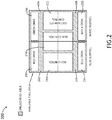
- the pixel 200 comprises four subpixels 202, 204, 206, 208. Each subpixel 202, 204, 206, 208 is driven by a corresponding current drive transistor 210, 214, 218, 220. In at least one embodiment, the current drive transistors 210, 214, 218, 220 may be disposed to maximize available space for control elements 212, 216, 222.
- one of the control elements 212, 216, 222 may comprise a combined control element 222 configured to control the brightness of two related subpixels 206, 208, either alternatively or in concert.
- the combined control element 222 may include a switching element / selection logic for determining which of the related subpixels 206, 208 to illuminate.
- the current drive transistors 210, 214, 218, 220 and control elements 212, 216, 222 may be embodied in a backplane, separate from an LED plane, such that the backplane may be configured to drive subpixels 202, 204, 206, 208 in any LED plane with substantially similar layout, regardless of the composition of the subpixels 202, 204, 206, 208.
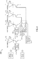
- FIG. 4 a block diagram of a pixel 400, including subpixels 402, 406, 410, 412, and control elements 404, 408, 414 according to an exemplary embodiment is shown.
- Each subpixel 402, 406, 410, 412 is driven by an independent current drive transistor, controlled via corresponding control element 404, 408, 414.
- One of the control elements 404, 408, 414 is configured to control the brightness level of two related subpixels 410, 412 in the alternative or in concert.
- the pixel 400 may comprise a red-blue-green-white subpixel layout, a green monochrome subpixel layout, a red-green-blue-green subpixel layout, or any other subpixel layout wherein at least two subpixels 402, 406, 410, 412 are sufficiently related to allow their brightness values to be set in the alternative or in concert.
- a switching element 416 comprises selection logic that receives a plurality of inputs to determine which of the two related subpixels 410, 412 to illuminate.
- the inputs may receive a set of bits indicating the type of LED plane (e.g. monochrome or red-green-blue-green) and whether a secondary green subpixel should be driven.
- the inputs may also comprise one or more input bits of other control elements 404, 408.
- the inputs may also comprise one or more input bits of other control elements 404, 408.
- least significant bits intended for a blue subpixel control element 408 may be received by the switching element 416.
- FIG. 3 One exemplary chart of inputs and corresponding outputs are shown in FIG. 3 (output "G” indicating corresponding related subpixel 404, 408 is illuminated and output "0" indicating it is not).
- a combined control element 414 will always drive both related pixels 410, 412.
- an input bit indicates a red-green-blue-green LED plane ("RGBG" equals 1 in FIG. 3 )
- the combined control element 414 will illuminate a secondary green subpixel in the related subpixels 410, 412 to the same brightness as a primary green subpixel if another bit indicates that the least significant bit of the blue sub pixel control element 408 should be used to determine which of the related subpixels 410, 412 to drive ("Video" equals 1 in FIG. 3 ).
- the least significant bit of a color channel is only an exemplary embodiment; any bit in the video stream may be used.
- the LED plane may be assumed to be a red-green-blue-white LED plane.
- a least significant bit of one or more control signals to the non-combined control elements 404, 408 may indicate if the combined control element 414 should illuminate the white subpixel 412 ("B0 equals 1 in FIG. 3 ).
- FIG. 5 shows a similar chart of digital inputs to the switching element 416 wherein the RGBG input is removed. The switching element 416 may still be addressable to illuminate one or both of the related subpixels 410, 412.
- a display according to the present disclosure may have a backplane with a 25% reduction in the number of control transistors; improving yield up to 25% and reducing recurring cost.
- the required chip area is also reduced, allowing larger, cheaper semiconductor node size to be used (75 nm or larger as compared to 65 nm), reducing process waste.
- space and complexity savings may allow for a corresponding increase in brightness control complexity from eight-bit to ten-bit.
Landscapes
- Engineering & Computer Science (AREA)
- Physics & Mathematics (AREA)
- Computer Hardware Design (AREA)
- General Physics & Mathematics (AREA)
- Theoretical Computer Science (AREA)
- Control Of Indicators Other Than Cathode Ray Tubes (AREA)
- Control Of El Displays (AREA)
Abstract
Description
- The present application claims the benefit under 35 U.S.C. § 119(e) of
U.S. Provisional App. No. 63/006,562 (filed April 7, 2020 - Helmet mounted or head worn micro-displays require high brightness and high resolution in a small area (such as a one-inch square). Some state-of-the-art displays include four subpixels that comprise each pixel. Such displays require separate control circuitry for each addressable display element.
- To enable the required brightness, a current drive transistor is required for each subpixel and occupies a significant portion of the area available for display control. High-quality graphics requires very fine control of gray scale (brightness levels) for each subpixel. Such control requires a complicated control circuit with many transistors. High transistor count leads to poor process yields and correspondingly high product costs. Simultaneously, the control transistors must be made very small to fit within the available space. Space constraints necessitate the use of very small geometry semiconductor processes with high recurring and non-recurring costs and waste.
- In one aspect, embodiments of the inventive concepts disclosed herein are directed to a display with subpixel LEDs where two of the subpixel LEDs are controlled via a shared control circuit and switching element. Switching element logic allows one set of brightness control transistors to alternatively control two subpixels. The driving and control elements of a display backplane are organized into pixels units of four driving elements and three control elements.
- In a further aspect, each pixel comprises two green subpixels controlled via the switching element. Alternatively, each pixel comprises a white subpixel that only illuminates when the colored pixels are off; the green and white subpixels are controlled via the switching element.
- It is to be understood that both the foregoing general description and the following detailed description are exemplary and explanatory only and should not restrict the scope of the claims. The accompanying drawings, which are incorporated in and constitute a part of the specification, illustrate exemplary embodiments of the inventive concepts disclosed herein and together with the general description, serve to explain the principles.
- The numerous advantages of the embodiments of the inventive concepts disclosed herein may be better understood by those skilled in the art by reference to the accompanying figures in which:
- FIG. 1
- shows a block diagram of a pixel, including subpixels, and control elements according to an exemplary embodiment;
- FIG. 2
- shows a block diagram of a pixel according to an exemplary embodiment;
- FIG. 3
- shows a chart of digital inputs and outputs for a switching element according to an exemplary embodiment;
- FIG. 4
- shows a block diagram of a pixel, including subpixels, and control elements according to an exemplary embodiment;
- FIG. 5
- shows a chart of digital inputs and outputs for a switching element according to an exemplary embodiment;
- Before explaining at least one embodiment of the inventive concepts disclosed herein in detail, it is to be understood that the inventive concepts are not limited in their application to the details of construction and the arrangement of the components or steps or methodologies set forth in the following description or illustrated in the drawings. In the following detailed description of embodiments of the instant inventive concepts, numerous specific details are set forth in order to provide a more thorough understanding of the inventive concepts. However, it will be apparent to one of ordinary skill in the art having the benefit of the instant disclosure that the inventive concepts disclosed herein may be practiced without these specific details. In other instances, well-known features may not be described in detail to avoid unnecessarily complicating the instant disclosure. The inventive concepts disclosed herein are capable of other embodiments or of being practiced or carried out in various ways. Also, it is to be understood that the phraseology and terminology employed herein is for the purpose of description and should not be regarded as limiting.
- As used herein a letter following a reference numeral is intended to reference an embodiment of the feature or element that may be similar, but not necessarily identical, to a previously described element or feature bearing the same reference numeral (e.g., 1, 1a, 1b). Such shorthand notations are used for purposes of convenience only, and should not be construed to limit the inventive concepts disclosed herein in any way unless expressly stated to the contrary.
- Further, unless expressly stated to the contrary, "or" refers to an inclusive or and not to an exclusive or. For example, a condition A or B is satisfied by anyone of the following: A is true (or present) and B is false (or not present), A is false (or not present) and B is true (or present), and both A and B are true (or present).
- In addition, use of the "a" or "an" are employed to describe elements and components of embodiments of the instant inventive concepts. This is done merely for convenience and to give a general sense of the inventive concepts, and "a" and "an" are intended to include one or at least one and the singular also includes the plural unless it is obvious that it is meant otherwise.
- Finally, as used herein any reference to "one embodiment," or "some embodiments" means that a particular element, feature, structure, or characteristic described in connection with the embodiment is included in at least one embodiment of the inventive concepts disclosed herein. The appearances of the phrase "in some embodiments" in various places in the specification are not necessarily all referring to the same embodiment, and embodiments of the inventive concepts disclosed may include one or more of the features expressly described or inherently present herein, or any combination of sub-combination of two or more such features, along with any other features which may not necessarily be expressly described or inherently present in the instant disclosure.
- Broadly, embodiments of the inventive concepts disclosed herein are directed to a display with subpixel LEDs where two of the subpixel LEDs are controlled via a shared control circuit and switching element. Switching element logic allows one set of brightness control transistors to alternatively control two subpixels. The driving and control elements of a display backplane are organized into pixels units of four driving elements and three control elements. The architecture of a pixel comprising four subpixels and the corresponding drive elements may be more fully understood with respect to
U.S. Patent App. No. 16/704322 - Referring to
FIG. 1 , a block diagram of apixel 100, includingsubpixels control elements subpixel subpixel corresponding control element control elements related subpixels - In at least one embodiment, the
pixel 100 comprises a first,red subpixel 102 controlled by afirst control element 104 and a second,blue subpixel 106 controlled by asecond control element 108. A third,green subpixel 110 and a fourth,white subpixel 112 are controlled by athird control element 114. Aswitching element 116 alternatively diverts a control signal to either the third,green subpixel 110 or the fourth,white subpixel 112 based on a set of inputs as more fully described herein. In such embodiment, the fourth,white subpixel 112 is never driven at the same time as theother subpixels - In at least one embodiment, the
pixel 100 comprises a first,red subpixel 102 controlled by afirst control element 104 and a second,blue subpixel 106 controlled by asecond control element 108. A third, primarygreen subpixel 110 and a fourth, secondarygreen subpixel 112 are controlled by athird control element 114. Aswitching element 116 may apply a control signal to the third, primarygreen subpixel 110 alone, or also to the fourth, secondarygreen subpixel 112 based on a set of inputs. In such embodiment, the fourth, secondarygreen subpixel 112, if driven, is driven at the same brightness as the third, primarygreen subpixel 110. - In at least one embodiment, where the display is monochrome, each
subpixel green subpixel control elements subpixel element 116 may be connected to and apply the same signal to eachsubpixel subpixels control elements related subpixels control element 114 via theswitching element 116. - In at least one embodiment, the
control elements element 116 may be embodied in a backplane while thesubpixels switching element 116 may be addressed via inputs to drive either or both of theconnected subpixels - Referring to
FIG. 2 , a block diagram of apixel 200 according to an exemplary embodiment is shown. Thepixel 200 comprises foursubpixels subpixel current drive transistor current drive transistors control elements - In at least one embodiment, one of the
control elements control element 222 configured to control the brightness of tworelated subpixels control element 222 may include a switching element / selection logic for determining which of therelated subpixels - In at least one embodiment, the
current drive transistors elements subpixels subpixels - Referring to
FIG. 4 , a block diagram of apixel 400, includingsubpixels elements subpixel corresponding control element control elements related subpixels pixel 400 may comprise a red-blue-green-white subpixel layout, a green monochrome subpixel layout, a red-green-blue-green subpixel layout, or any other subpixel layout wherein at least twosubpixels - In at least one embodiment, a
switching element 416 comprises selection logic that receives a plurality of inputs to determine which of the tworelated subpixels - In at least one embodiment, the inputs may also comprise one or more input bits of
other control elements 404, 408. For example, least significant bits intended for a blue subpixel control element 408 may be received by the switchingelement 416. One exemplary chart of inputs and corresponding outputs are shown inFIG. 3 (output "G" indicating correspondingrelated subpixel 404, 408 is illuminated and output "0" indicating it is not). - In one exemplary embodiment, where an input bit indicates a monochrome LED plane ("Mono" equals 1 in
FIG. 3 ), a combinedcontrol element 414 will always drive bothrelated pixels FIG. 3 ), the combinedcontrol element 414 will illuminate a secondary green subpixel in therelated subpixels related subpixels FIG. 3 ). It may be appreciated that the least significant bit of a color channel is only an exemplary embodiment; any bit in the video stream may be used. Where none of the Mono, RBGB, or Video inputs indicates those states, the LED plane may be assumed to be a red-green-blue-white LED plane. In that case, because none of the colorspecific subpixels white subpixel 412, a least significant bit of one or more control signals to thenon-combined control elements 404, 408 may indicate if the combinedcontrol element 414 should illuminate the white subpixel 412 ("B0 equals 1 inFIG. 3 ). It may be appreciated that the actual values may depend on the architecture of the selection logic in theswitching element 416. For clarity and simplicity,FIG. 5 shows a similar chart of digital inputs to theswitching element 416 wherein the RGBG input is removed. The switchingelement 416 may still be addressable to illuminate one or both of therelated subpixels - A display according to the present disclosure may have a backplane with a 25% reduction in the number of control transistors; improving yield up to 25% and reducing recurring cost. The required chip area is also reduced, allowing larger, cheaper semiconductor node size to be used (75 nm or larger as compared to 65 nm), reducing process waste. Furthermore, space and complexity savings may allow for a corresponding increase in brightness control complexity from eight-bit to ten-bit.
- It should be appreciated that while exemplary embodiments described herein were directed to pixels comprised of four subpixels, other embodiments are envisioned. For example, five or six subpixels are also possible. Any embodiment wherein at least two subpixels are controlled by a single control element is envisioned. Furthermore, multiple sets of related subpixels within a pixel may each be controlled a separate single control element.
- It is believed that the inventive concepts disclosed herein and many of their attendant advantages will be understood by the foregoing description of embodiments of the inventive concepts disclosed, and it will be apparent that various changes may be made in the form, construction, and arrangement of the components thereof without departing from the broad scope of the inventive concepts disclosed herein or without sacrificing all of their material advantages; and individual features from various embodiments may be combined to arrive at other embodiments. The form herein before described being merely an explanatory embodiment thereof, it is the intention of the following claims to encompass and include such changes. Furthermore, any of the features disclosed in relation to any of the individual embodiments may be incorporated into any other embodiment.
Claims (15)
- A backplane element for a display comprising: a plurality of pixel driving elements, each pixel driving element comprising:four subpixel power elements, each configured to drive a subpixel;three subpixel control elements; anda control switch (116),wherein:a first subpixel control element (104) is configured to set a brightness level of a first subpixel (102);a second subpixel control element (108) is configured to set a brightness level of a second subpixel (106);a third subpixel control element (114) is configured to set a brightness level of a third subpixel (110) or a fourth subpixel (112); andthe control switch is configured to switch the third subpixel control element between the third subpixel and the fourth subpixel.
- The backplane element of Claim 1, wherein the control switch (116) comprises a plurality of gates, the plurality of gates being driven by a plurality of inputs.
- The backplane element of Claim 2, wherein one of the plurality of inputs comprises bits in a video stream, each bit associated with one of the plurality of pixel driving elements such that the plurality of gates for each pixel driving element is individually addressable via the video stream.
- The backplane element of any of Claims 1-3, wherein the plurality of pixel driving elements comprise a semiconductor node size of at least 75 nm.
- The backplane element of any of Claims 1-4, wherein the three subpixel control elements are each configured to receive a ten-bit brightness level control signal.
- A display comprising:a. an LED plane comprising a plurality of pixels, each pixel comprising four subpixel LEDs; andb. a backplane element as claimed in claim 1 configured to drive the subpixel LEDs in the LED plane.
- The display of Claim 6, wherein the control switch (116) comprises a plurality of gates, the plurality of gates being driven by a plurality of inputs.
- The display of Claim 7, wherein one of the plurality of inputs comprises bits in a video stream, each bit associated with one of the pixels such that the plurality of gates for each pixel is individually addressable via the video stream.
- The display of any of Claims 6-8, wherein the plurality of pixel driving elements comprise a semiconductor node size of at least 75 nm.
- The display of any of Claims 6-9, wherein the three subpixel control elements are each configured to receive a ten-bit brightness level control signal.
- The display of Claim 6, wherein each pixel of the LED plane comprises four green subpixel LEDs.
- The display of Claim 6, wherein each pixel of the LED plane comprises one red subpixel LED, one blue subpixel LED, and two green subpixel LEDs.
- The display of Claim 12, wherein the two green subpixel LEDs are controlled via the third subpixel control element.
- The display of Claim 6, wherein each pixel of the LED plane comprises one red subpixel LED, one blue subpixel LED, one green subpixel LED, and one white subpixel LED.
- The display of Claim 14, wherein the green subpixel LED and the white subpixel LED are controlled via the third subpixel control element.
Applications Claiming Priority (2)
| Application Number | Priority Date | Filing Date | Title |
|---|---|---|---|
| US202063006562P | 2020-04-07 | 2020-04-07 | |
| US17/210,118 US11386835B2 (en) | 2020-04-07 | 2021-03-23 | Pixel control architecture for micro-LED micro-display with reduced transistor count |
Publications (1)
| Publication Number | Publication Date |
|---|---|
| EP3893235A1 true EP3893235A1 (en) | 2021-10-13 |
Family
ID=75426490
Family Applications (1)
| Application Number | Title | Priority Date | Filing Date |
|---|---|---|---|
| EP21167219.1A Withdrawn EP3893235A1 (en) | 2020-04-07 | 2021-04-07 | Pixel control architecture for micro-led micro-display with reduced transistor count |
Country Status (2)
| Country | Link |
|---|---|
| US (1) | US11386835B2 (en) |
| EP (1) | EP3893235A1 (en) |
Families Citing this family (1)
| Publication number | Priority date | Publication date | Assignee | Title |
|---|---|---|---|---|
| KR20250125777A (en) * | 2024-02-15 | 2025-08-22 | 엘지디스플레이 주식회사 | Micro display apparatus |
Citations (4)
| Publication number | Priority date | Publication date | Assignee | Title |
|---|---|---|---|---|
| US20150332628A1 (en) * | 2013-09-03 | 2015-11-19 | Boe Technology Group Co., Ltd. | Pixel circuit, its driving method, array substrate and display device |
| US20170345370A1 (en) * | 2016-05-31 | 2017-11-30 | Universal Display Corporation | Novel Architecture for Very High Resolution AMOLED Display Backplane |
| US20180293942A1 (en) * | 2016-01-13 | 2018-10-11 | Shenzhen Yunyinggu Technology Co., Ltd. | Apparatus and method for pixel data reordering |
| CN110706653A (en) * | 2019-10-21 | 2020-01-17 | 京东方科技集团股份有限公司 | Driving circuit, display panel, driving method and display device |
Family Cites Families (4)
| Publication number | Priority date | Publication date | Assignee | Title |
|---|---|---|---|---|
| WO2005091263A1 (en) * | 2004-03-19 | 2005-09-29 | Koninklijke Philips Electronics N.V. | Active matrix display with pixel to pixel non-uniformity improvement at low luminance level |
| JP5377057B2 (en) * | 2008-06-30 | 2013-12-25 | 株式会社ジャパンディスプレイ | Image display apparatus driving method, image display apparatus assembly and driving method thereof |
| JP2014186257A (en) * | 2013-03-25 | 2014-10-02 | Sony Corp | Display device and electronic apparatus |
| JP2014212080A (en) * | 2013-04-19 | 2014-11-13 | 株式会社ジャパンディスプレイ | Display device |
-
2021
- 2021-03-23 US US17/210,118 patent/US11386835B2/en active Active
- 2021-04-07 EP EP21167219.1A patent/EP3893235A1/en not_active Withdrawn
Patent Citations (5)
| Publication number | Priority date | Publication date | Assignee | Title |
|---|---|---|---|---|
| US20150332628A1 (en) * | 2013-09-03 | 2015-11-19 | Boe Technology Group Co., Ltd. | Pixel circuit, its driving method, array substrate and display device |
| US20180293942A1 (en) * | 2016-01-13 | 2018-10-11 | Shenzhen Yunyinggu Technology Co., Ltd. | Apparatus and method for pixel data reordering |
| US20170345370A1 (en) * | 2016-05-31 | 2017-11-30 | Universal Display Corporation | Novel Architecture for Very High Resolution AMOLED Display Backplane |
| CN110706653A (en) * | 2019-10-21 | 2020-01-17 | 京东方科技集团股份有限公司 | Driving circuit, display panel, driving method and display device |
| US20210118366A1 (en) * | 2019-10-21 | 2021-04-22 | Boe Technology Group Co., Ltd. | Driving circuit, display panel, driving method and display device |
Also Published As
| Publication number | Publication date |
|---|---|
| US20210312857A1 (en) | 2021-10-07 |
| US11386835B2 (en) | 2022-07-12 |
Similar Documents
| Publication | Publication Date | Title |
|---|---|---|
| US8537092B2 (en) | Shared buffer display panel drive methods and systems | |
| US10614742B2 (en) | Pixel structure, array substrate, display device and method for driving the display device | |
| US6323871B1 (en) | Display device and its driving method | |
| CN111986604B (en) | Pixel driving structure and display device | |
| US20150161927A1 (en) | Driving apparatus with 1:2 mux for 2-column inversion scheme | |
| US8179345B2 (en) | Shared buffer display panel drive methods and systems | |
| US12315438B2 (en) | Column interchangeable demultiplexer structure in displays | |
| US10692436B2 (en) | Display panel and display device | |
| CN219418467U (en) | LED display screen control system and display device | |
| US11386835B2 (en) | Pixel control architecture for micro-LED micro-display with reduced transistor count | |
| CN111369931B (en) | Display module, driving method thereof and display device | |
| US11694611B2 (en) | Four-way dual scanning electronic display board capable of scan control | |
| US12211884B2 (en) | Micro-LED display device | |
| CN113012645A (en) | Gamma reference voltage output circuit of display device | |
| CN100511382C (en) | Method and system for shared buffer display panel drive | |
| CN113012627B (en) | Constant current drive circuit and display panel | |
| JPH04241384A (en) | Color led display device | |
| JP3564359B2 (en) | Light emitting diode drive circuit | |
| US8471806B2 (en) | Display panel drive circuit and display | |
| US11908387B1 (en) | Display backplane with shared drivers for light source devices | |
| US20250124847A1 (en) | Display apparatus and method of driving display panel using the same | |
| US20260080837A1 (en) | Display Device | |
| US20050212739A1 (en) | Driving circuit for liquid crystal device | |
| US12615702B2 (en) | Luminous film, display element and method for operating a luminous film | |
| KR102895204B1 (en) | Data driving device and panel driving method of data driving device |
Legal Events
| Date | Code | Title | Description |
|---|---|---|---|
| PUAI | Public reference made under article 153(3) epc to a published international application that has entered the european phase |
Free format text: ORIGINAL CODE: 0009012 |
|
| STAA | Information on the status of an ep patent application or granted ep patent |
Free format text: STATUS: THE APPLICATION HAS BEEN PUBLISHED |
|
| AK | Designated contracting states |
Kind code of ref document: A1 Designated state(s): AL AT BE BG CH CY CZ DE DK EE ES FI FR GB GR HR HU IE IS IT LI LT LU LV MC MK MT NL NO PL PT RO RS SE SI SK SM TR |
|
| STAA | Information on the status of an ep patent application or granted ep patent |
Free format text: STATUS: REQUEST FOR EXAMINATION WAS MADE |
|
| 17P | Request for examination filed |
Effective date: 20220407 |
|
| RBV | Designated contracting states (corrected) |
Designated state(s): AL AT BE BG CH CY CZ DE DK EE ES FI FR GB GR HR HU IE IS IT LI LT LU LV MC MK MT NL NO PL PT RO RS SE SI SK SM TR |
|
| STAA | Information on the status of an ep patent application or granted ep patent |
Free format text: STATUS: EXAMINATION IS IN PROGRESS |
|
| 17Q | First examination report despatched |
Effective date: 20230811 |
|
| STAA | Information on the status of an ep patent application or granted ep patent |
Free format text: STATUS: THE APPLICATION HAS BEEN WITHDRAWN |
|
| 18W | Application withdrawn |
Effective date: 20251205 |