EP3893166A1 - Device and method for convolution operation - Google Patents
Device and method for convolution operation Download PDFInfo
- Publication number
- EP3893166A1 EP3893166A1 EP20876067.8A EP20876067A EP3893166A1 EP 3893166 A1 EP3893166 A1 EP 3893166A1 EP 20876067 A EP20876067 A EP 20876067A EP 3893166 A1 EP3893166 A1 EP 3893166A1
- Authority
- EP
- European Patent Office
- Prior art keywords
- read control
- matrix
- distributed caches
- elements
- distributed
- Prior art date
- Legal status (The legal status is an assumption and is not a legal conclusion. Google has not performed a legal analysis and makes no representation as to the accuracy of the status listed.)
- Granted
Links
Images

Classifications
-
- G—PHYSICS
- G06—COMPUTING OR CALCULATING; COUNTING
- G06F—ELECTRIC DIGITAL DATA PROCESSING
- G06F7/00—Methods or arrangements for processing data by operating upon the order or content of the data handled
- G06F7/38—Methods or arrangements for performing computations using exclusively denominational number representation, e.g. using binary, ternary, decimal representation
- G06F7/48—Methods or arrangements for performing computations using exclusively denominational number representation, e.g. using binary, ternary, decimal representation using non-contact-making devices, e.g. tube, solid state device; using unspecified devices
- G06F7/544—Methods or arrangements for performing computations using exclusively denominational number representation, e.g. using binary, ternary, decimal representation using non-contact-making devices, e.g. tube, solid state device; using unspecified devices for evaluating functions by calculation
- G06F7/5443—Sum of products
-
- G—PHYSICS
- G06—COMPUTING OR CALCULATING; COUNTING
- G06F—ELECTRIC DIGITAL DATA PROCESSING
- G06F17/00—Digital computing or data processing equipment or methods, specially adapted for specific functions
- G06F17/10—Complex mathematical operations
- G06F17/15—Correlation function computation including computation of convolution operations
- G06F17/153—Multidimensional correlation or convolution
-
- G—PHYSICS
- G06—COMPUTING OR CALCULATING; COUNTING
- G06F—ELECTRIC DIGITAL DATA PROCESSING
- G06F17/00—Digital computing or data processing equipment or methods, specially adapted for specific functions
- G06F17/10—Complex mathematical operations
- G06F17/16—Matrix or vector computation, e.g. matrix-matrix or matrix-vector multiplication, matrix factorization
-
- G—PHYSICS
- G06—COMPUTING OR CALCULATING; COUNTING
- G06F—ELECTRIC DIGITAL DATA PROCESSING
- G06F7/00—Methods or arrangements for processing data by operating upon the order or content of the data handled
- G06F7/38—Methods or arrangements for performing computations using exclusively denominational number representation, e.g. using binary, ternary, decimal representation
- G06F7/48—Methods or arrangements for performing computations using exclusively denominational number representation, e.g. using binary, ternary, decimal representation using non-contact-making devices, e.g. tube, solid state device; using unspecified devices
- G06F7/52—Multiplying; Dividing
-
- G—PHYSICS
- G06—COMPUTING OR CALCULATING; COUNTING
- G06N—COMPUTING ARRANGEMENTS BASED ON SPECIFIC COMPUTATIONAL MODELS
- G06N3/00—Computing arrangements based on biological models
- G06N3/02—Neural networks
- G06N3/06—Physical realisation, i.e. hardware implementation of neural networks, neurons or parts of neurons
- G06N3/063—Physical realisation, i.e. hardware implementation of neural networks, neurons or parts of neurons using electronic means
-
- G—PHYSICS
- G06—COMPUTING OR CALCULATING; COUNTING
- G06N—COMPUTING ARRANGEMENTS BASED ON SPECIFIC COMPUTATIONAL MODELS
- G06N3/00—Computing arrangements based on biological models
- G06N3/02—Neural networks
- G06N3/08—Learning methods
Definitions
- Embodiments of the present disclosure mainly relate to the field of data processing, and more specifically to an apparatus and a method for convolution operation.
- Convolution algorithm is the core algorithm of the convolutional neural network, and accounts for 90% of operation time of a convolutional neural network. Therefore, convolution operations are the primary optimization objects for designing a neural network hardware accelerator based on a field programmable gate array (FPGA). Hardware circuit design for convolution algorithm directly affects resource usage of the hardware accelerator and computing power that can be achieved.
- FPGA field programmable gate array
- An adder tree structure which is defined based on a convolution algorithm, is employed in one of conventional solutions.
- adder tree for convolution six dimensions of convolution calculation are fully expanded based on a 6-layer loop characteristics of the convolution algorithm.
- multiplication is first performed between corresponding points in a filter matrix and in an input data matrix, and then accumulation is performed per point within a window of the filter matrix and in the direction of a channel.
- This implementation is simple and straightforward. However, this implementation also has obvious shortcomings. If the dimension of computing is increased, the depth of an adder needs to be increased, and the amount of consumed resource increases exponentially, which is unacceptable for a resource-sensitive FPGA.
- an apparatus and a method for convolution operation with improved performance are provided.
- an apparatus for convolution operation comprises: a plurality of multipliers configured to receive matrix elements from a first matrix and from a second matrix, respectively, and to generate a plurality of product elements, wherein each product element of the plurality of product element is obtained by multiplying, by a respective multiplier, a number of matrix elements of the first matrix and corresponding matrix elements of the second matrix; a plurality of distributed caches respectively coupled to the plurality of multipliers and each distributed cache of the plurality of distributed caches comprising a plurality of cache units, wherein the plurality of distributed caches is each configured to store a respective one of the plurality of product elements in a respective cache unit thereof; a register delay chain coupled to the plurality of distributed caches and comprising a plurality of registers coupled in series, wherein the register delay chain is configured to receive a read control signal, to delay the read control signal per stage to output a plurality of per-stage delayed read control signals, and to respectively provide, to the plurality of distributed
- a method for convolution operation comprises: receiving matrix elements from a first matrix and from a second matrix, and multiplying matrix elements of the first matrix with corresponding matrix elements of the second matrix to generate a plurality of product elements; respectively storing the plurality of product elements in respective cache units of a plurality of distributed caches; receiving a read control signal, delaying the read control signal per stage to output a plurality of per-stage delayed read control signals, and respectively providing, to the plurality of distributed caches, the read control signal and the plurality of per-stage delayed read control signals; receiving, from the plurality of distributed caches, product elements in cache units corresponding to the read control signal and the plurality of per-stage delayed read control signals; and generating accumulation data based on the received product elements in the respective cache units of the plurality of distributed caches.
- the term “comprise” and similar terms should be understood as non-exclusive inclusion, that is, “including but not limited to”.
- the term “based on” should be understood as “at least partially based on”.
- the terms “an embodiment” or “the embodiment” should be understood as “at least one embodiment”.
- the terms “first”, “second”, and the like may refer to different or the same objects. Other explicit and implicit definitions may also be included below.
- a systolic array implementation involves a spatially expansion of the five dimensions of a convolution calculation and a temporally expansion of the dimension of a channel.
- This solution can effectively utilize resources because when the dimensions of convolution calculation increases, resources required for the systolic array implementation do not need to be increased, but only the accumulation in the direction of the channel is extended in the time dimension.
- This conventional solution implements a delay chain in the dimension of the channel by using register resources in an FPGA. For example, in this conventional solution, registers are used to delay intermediate calculation data by six clock cycles before accumulation.
- FPGA overall resources usually comprise a lookup table (LUT), an LUT memory (LUTM), a register, and a digital signal processor (DSP). Excessive consumption of register resources will cause the unbalanced use of the FPGA overall resources, which leads to the "bucket effect”.
- LUT lookup table
- LUT memory LUT memory
- DSP digital signal processor
- the embodiments of the present disclosure provide a convolution operation solution that can save hardware resources and balance the required hardware resources.
- a product of two corresponding matrix elements, each in one matrix is stored in a respective cache unit of a plurality of distributed caches.
- a read control signal for the respective cache unit of the plurality of distributed caches is delayed per stage by a register delay chain.
- An accumulation result is generated based on products which are received from the plurality of distributed caches and which were stored in respective cache units corresponding to read control signals.
- a functionality similar to that of a register delay chain for intermediate calculation data in the systolic array structure is achieved, which facilitates the implementation of convolution operation. Therefore, the read control signal is delayed per stage while the products are maintained in the distributed caches, so as to prevent the transfer of intermediate calculation data by the register delay chain as in the systolic array structure. In this way, the convolution operation solution according to the embodiments of the present disclosure reduces overall power consumption while saving register resources.
- utilizing distributed caches that are usually idle, such as LUTMs in an FPGA can save overall design resources and achieve resource balancing.
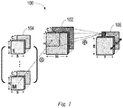
- Fig. 1 is a schematic diagram showing a model 100 for convolution operation.
- an input data set matrix comprises a plurality of input data matrices 102
- a filter set matrix comprises a plurality of filter matrices 104.
- the input data matrix 102 is a matrix of various data output by a sensor
- the filter matrix 104 is a window matrix for performing a convolution operation.
- annotation C shown in Fig. 1 represents the number of channels of input data matrices 102 in the input data set matrix or the number of channels of filter matrices 104 in the filter set matrix.
- the dimensions of each input data matrix 102 are H ⁇ W
- the dimensions of each filter matrix 104 are R ⁇ S.
- convolution operations are performed on a plurality of filter matrices 104 in each filter set matrix and the plurality of input data matrices 102 in the input data set matrix, to generate one output matrix 106. Therefore, when a plurality of filter set matrices are used for convolution operation, a plurality of output channels of output matrices 106 are generated. For example, when M filter set matrices are used, M channels of output matrices 106 are generated, and the dimensions of each output matrix 106 are E ⁇ F.
- performing a convolution operation on a filter matrix 104 and a corresponding input data matrix 102 at one window means multiplying matrix elements in a submatrix of the input data matrix 102 that corresponds to the window by corresponding matrix elements of the filter matrix 104 to generate product elements, and these product elements are summed up to generate an accumulation data.
- convolution operations are performed on C filter matrices 104 and C input data matrices 102 at the window shown to generate C pieces of accumulation data, and these C pieces of accumulation data are summed up to generate one matrix element in the output matrix 106.
- Matrix elements in the output matrix 106 are generated by shifting the window within the input data matrix 102.
- M filter set matrices instead of one matrix are used, M output matrices 106 are generated as described above for use in calculation in following stages.
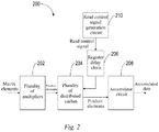
- Fig. 2 is a block diagram showing an apparatus 200 for convolution operation according to an embodiment of the present disclosure.
- the apparatus 200 comprises a plurality of multipliers 202, a plurality of distributed caches 204, a register delay chain 206, and an accumulator circuit 208.
- the plurality of multipliers 202 are configured to receive matrix elements from a first matrix and from a second matrix, respectively, and to generate a plurality of product elements, wherein each product element of the plurality of product element is obtained by multiplying, by a respective multiplier, a number of matrix elements of the first matrix and corresponding matrix elements of the second matrix.
- the first matrix is an input data set matrix of input data matrices including a plurality of channels
- the second matrix is a filter set matrix of filter matrices including a plurality of channels.
- the plurality of multipliers 202 receive matrix elements and generate a plurality of product elements.
- the input data set matrix includes input data matrices with C channels
- the filter set matrix includes filter matrices with C channels.
- the plurality of multipliers 202 receive matrix elements of input data matrix from one channel and of filter matrix from one corresponding channel, and generate a plurality of product elements.
- the plurality of distributed caches 204 are respectively coupled to the plurality of multipliers 202 and each comprise a plurality of cache units.
- the plurality of distributed caches 204 are each configured to store a respective one of the plurality of product elements in a respective cache unit thereof.
- the plurality of distributed caches 204 receive a plurality of product elements from a plurality of multipliers 202, and store each of the plurality of product elements in a respective cache unit that correspond to the clock cycle in a respective one of the plurality of distributed caches, respectively.
- each of the plurality of distributed caches 204 sequentially stores a plurality of product elements in respective cache units thereof.
- the register delay chain 206 is coupled to the plurality of distributed caches 204 and includes a plurality of registers coupled in series.
- the register delay chain 206 is configured to receive a read control signal, delay the read control signal per stage to output a plurality of per-stage delayed read control signals, and respectively provide, to the plurality of distributed caches 204, the read control signal and the plurality of per-stage delayed read control signals.
- the register delay chain 206 receives a read control signal which corresponds to a respective cache unit of each distributed cache.
- a first distributed cache in the plurality of distributed caches 204 receives an undelayed read control signal.
- each register in the register delay chain 206 delays a read control signal received by the register, and provides, in a next clock cycle, the delayed read control signal to the corresponding cache unit and a register of the next stage.
- the accumulator circuit 208 is coupled to the plurality of distributed caches 204.
- the accumulator circuit 208 is configured to receive, from the plurality of distributed caches 204, product elements in cache units corresponding to the read control signal and the plurality of per-stage delayed read control signals, and to generate an accumulation data based on the received product elements in the respective cache units of the plurality of distributed caches.
- the accumulator circuit 208 receives, from the plurality of distributed caches 204, product elements in cache units corresponding to the read control signals received by the distributed caches.
- the accumulator circuit 208 accumulates product elements received from cache units of the plurality of distributed caches 204 that correspond to the same clock cycle.
- the accumulator circuit 208 accumulates product elements generated in the same clock cycle. In some embodiments, when the input data set matrix includes input data matrices with C channels and the filter set matrix includes filter matrices with C channels, after C clock cycles, the accumulator circuit 208 outputs a result of a convolution operation on one channel of input data matrix and one corresponding channel of filter matrix within a certain window, and after another clock cycle, the accumulator circuit 208 outputs a result of a convolution operation on another channel of input data matrix and one corresponding channel of filter matrix within a certain window, and so on.
- the apparatus 200 may further include a read control signal generation circuit 210.
- the read control signal generation circuit 210 is configured to sequentially generate read control signals that correspond to the plurality of cache units of the plurality of distributed caches, respectively 204.
- the read control signal generation circuit 210 in each clock cycle of a plurality of clock cycles, the read control signal generation circuit 210 generates read control signals corresponding to the respective cache units of the plurality of distributed caches 204.
- the read control signal generation circuit 210 in each clock cycle of a plurality of clock cycles, the read control signal generation circuit 210 generates a read control signal that includes a read address for one of the plurality of cache units, and increase the read address by one address unit in a next clock cycle.
- the read address corresponds to a cache unit, a clock cycle phase, and a product element generated in the clock cycle.
- the plurality of distributed caches 204 in response to receiving, by each of the plurality of distributed caches 204, the read control signal and the plurality of per-stage delayed read control signals, the plurality of distributed caches 204 output, to the accumulator circuit 208, product elements in cache units corresponding to the read address in the read control signal.
- an apparatus 200 by configuring a plurality of distributed caches and a register delay chain for read control signals for the plurality of distributed caches, the read control signal are delayed per stage while the products are maintained in the distributed caches, so as to prevent the transfer of intermediate calculation data by the register delay chain as in the systolic array structure. In this way, an apparatus 200 according to embodiments of the present disclosure reduces overall power consumption while saving register resources.
- the apparatus 200 is included in an FPGA. In an alternative embodiment, the apparatus 200 is included in an application-specific integrated circuit.
- each distributed cache is an LUTM resource in the FPGA.
- the FGPA is a Xilinx FPGA.
- a usually idle LUTM in the FPGA is used as the distributed cache, such that overall design resources are saved and resource balancing is achieved.
- the LUTM is easily operated and does not involve complex control logic, a higher design dominant frequency can be supported, and the overall computing power of a neural network accelerator can be improved.
- Fig. 3 is a schematic diagram showing an apparatus 300 for convolution operation according to an embodiment of the present disclosure.
- the apparatus 300 of Fig. 3 includes a plurality of multipliers 202, a plurality of distributed caches 204, a register delay chain 206, and an accumulator circuit 208.
- the apparatus 300 may be considered as an implementation of the apparatus 200. It should be understood that for simplicity of illustration, Fig. 3 shows a read control signal ADDR_n without illustrating the configuration of any read control signal generation circuit 210 .
- the read control signal generation circuit 210 can be implemented by any circuit known to the art.
- the plurality of multipliers 202 includes multipliers M0 to M15
- the plurality of distributed caches 204 includes distributed caches LUTMO to LUTM15
- the register delay chain 206 includes a plurality of registers reg1 to reg15
- the accumulator circuit 208 includes a multiplexer MUL module and accumulators ACC0 to ACC15.
- matrix elements w0 to w15 of a filter matrix are input to the multipliers M0 to M15, respectively, and the corresponding matrix elements i0 to i15 of an input data matrix are input to the multipliers M0 to M15, respectively.
- the distributed caches LUTM0 to LUTM15 each include a plurality of cache units Data0 to Data15. It should be understood that although Fig. 3 shows the number of various components, the apparatus 300 according to this embodiment of the present disclosure may include any other number of various components.
- the number of multipliers M0 to M15 is equal to the number of matrix elements in the filter matrix. In some embodiments, the number of distributed caches LUTM0 to LUTM15 is equal to the number of matrix elements in the filter matrix. In some embodiments, the number of cache units Data0 to Data15 of each of the distributed caches LUTM0 to LUTM15 is equal to the number of channels of filter matrices. In some embodiments, the number of accumulators ACC0 to ACC15 is equal to the number of cache units Data0 to Data15. In some embodiments, the number of registers reg1 to reg15 is less than the number of distributed caches LUTM0 to LUTM15 by a predetermined value. For example, the determined value is 1. As an example, in Fig. 3 , the number R ⁇ S of matrix elements of the filter matrix is equal to 16, and the number C of channels of filter matrices is equal to 16.
- the multipliers M0 to M15 are coupled to the distributed caches LUTM0 to LUTM15, respectively.
- the registers reg1 to reg15 are coupled in series with each other to form a delay chain, the register reg1 receives the read control signal ADDR_n as an input to the delay chain, and outputs of the registers reg1 to regl5 are coupled to the distributed caches LUTM1 to LUTM15, respectively.
- the distributed caches LUTM0 to LUTM15 are coupled to the multiplexer MUL module.
- each of the distributed caches LUTM0 to LUTM15 is a ring cache.
- the multiplexer MUL module is coupled to the accumulators ACC0 to ACC15.
- Each accumulator includes an adder and a register, the output of the adder being coupled to the register while the output of the register being coupled to the adder as one input of the adder to achieve accumulation.
- Each of the outputs of the multiplexer MUL module is coupled to the other input of a corresponding adder.
- the accumulator ACC0 includes an adder dsp0 and a register Reg0.
- the accumulator ACC1 includes an adder dsp1 and a register Reg1.
- the accumulator ACC15 includes an adder dsp15 and a register Reg15.
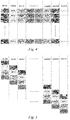
- Fig. 4 is a schematic diagram showing matrix elements that are input in various clock cycles and product elements that are generated in the clock cycles according to an embodiment of the present disclosure.
- Fig. 5 is a schematic diagram showing product elements that are read in the respective clock cycles according to an embodiment of the present disclosure.
- the multipliers M0 to M15 receive the matrix elements w0 to w15 and the matrix elements i0 to i15 in each clock cycle of a plurality of clock cycles clock0 to clock15, to generate product elements wo*i0 to w15*i15.
- each of the distributed caches LUTM0 to LUTM15 store a respective one of product elements wo*i0 to w15*i15 in a respective cache unit, which corresponds to the present clock cycle, of cache units Data0 to Data15 in the distributed caches, respectively.
- each the distributed caches LUTM0 to LUTM15 stores, in a cache unit Data0 thereof, a respective one of product elements wo*i0 to w15*i15 generated in clock cycle clock0. Further, each of the distributed caches LUTM0 to LUTM15 stores, in a cache unit Data1 thereof, a respective one of product elements wo*i0 to w15*i15 generated in clock cycle clock1. Analogously, each of the distributed caches LUTM0 to LUTM15 stores, in a cache units Data15 thereof, a respective one of product elements wo*i0 to w15*i15 generated in clock cycle clockl5.
- the 17th clock cycle clock16 may be considered as the start of a cycle of a convolution operation on the filter matrix and the input data matrix after the filter matrix is shifted to a next window position.
- a read control signal ADDR_n is generated in each of the plurality of clock cycles clock0 to clock15, where n is less than or equal to 0 and greater than or equal to 15.
- a read control signal ADDR_0 is generated in clock cycle clock0, which corresponds to a cache unit Data0 and is used for reading a respective product element in cache unit Data0 of a respective distributed cache
- a read control signal ADDR_1 is generated in clock cycle clock1, which corresponds to cache unit Data1 and is used for reading a respective product element in a cache unit Data1 of a respective distributed cache.
- a read control signal ADDR_15 is generated in clock cycle clock15, which corresponds to cache unit Data15 and is used for reading a respective product element in a cache unit Data15 of a respective distributed cache.
- the read control signal ADDR_0 generated in clock cycle clock0 is provided to the distributed cache LUTM0, and the product element wo*i0 in the cache unit Data0 of the distributed cache LUTM0 is read in clock cycle clock0.
- the read control signal ADDR_0 generated in clock cycle clock0 is input to the register reg1, and the register reg1 delays the read control signal ADDR_0.
- the register reg1 stores the read control signal ADDR_0 in clock cycle clock0, and outputs the read control signal ADDR_0 in the next clock cycle clock1.
- the register provides the delayed read control signal ADDR_0 to the distributed cache LUTM1 in the next clock cycle clock1, and the product element w1*il in the cache unit Data0 of the distributed cache LUTM1 is read in clock cycle clock1.
- the read control signal ADDR_1 generated in clock cycle clock1 is provided to the distributed cache LUTM0, and the product element wo*i0 in the cache unit Data1 of the distributed cache LUTM0 is read in clock cycle clockl.
- the read control signal ADDR_0 is input to the register reg2, and the register reg2 delays the read control signal ADDR_0; the read control signal ADDR_1 is input to the register reg1, and the register reg1 delays the read control signal ADDR_1.
- the product element w2*i2 in the cache unit Data0 of the distributed cache LUTM2 the product element w1*i1 in the cache unit Data1 of the distributed cache LUTM1, and the product element w0*i0 in the cache unit Data2 of the distributed cache LUTM0 are read.
- the product element w15*i15 in the cache unit Data0 of the distributed cache 5 the product element w14*i14 in the cache unit Data1 of the distributed cache LUTM14, ..., and the product element w0*i0 in the cache unit Data15 of the distributed cache LUTM0 are read.
- Fig. 3 shows a respective product element in a cache unit Data15, Data14, ..., Data0 that are received by the multiplexer MUL module in clock cycle clockl5.
- the multiplexer MUL module receives the product element wo*i0 in the cache unit Data0 of the distributed cache LUTM0, and provides the product element wo*i0 to the accumulator ACC0 corresponding to the cache unit Data0.
- the adder dsp0 in the accumulator ACC0 adds up the product element wo*i0 and null data, and stores an accumulation result in the register Reg0.
- the multiplexer MUL module receives the product element w1*i1 in the cache unit Data0 of the distributed cache LUTM1 and the product element wo*i0 in the cache unit Data1 of the distributed cache LUTM0, provides the product element w1*i1 in the cache unit Data0 of the distributed cache LUTM1 to the accumulator ACC0 corresponding to the cache unit Data0, and provides the product element wo*i0 in the cache unit Data1 of the distributed cache LUTM0 to the accumulator ACC1 corresponding to the cache unit Data1.
- the adder dsp0 in the accumulator ACC0 adds up the product element w1*i1 and the accumulation data generated in clock cycle clock0, and stores new accumulation data in the register Reg0
- the adder dsp1 in the accumulator ACC1 adds up the product element wo*i0 and null data, and stores an accumulation result in the register Reg1.
- the adder dsp0 in the accumulator ACC0 adds up the product element w15*i15 and the accumulation data generated in clock cycle clock14 , and stores new accumulation data in the register Reg0. In this way, the sum of a respective product element w0*i0 to w15*i15 generated in clock cycle clock0, that is, the result of the convolution operation, is obtained.
- the accumulator ACC0 outputs the result of the convolution operation on the respective matrix elements of the two matrices that are input in clock cycle clock0.
- the adder dsp1 in the accumulator ACC1 adds up the product element w15*i15 and the accumulation data generated in clock cycle clock15, and stores new accumulation data in the register Reg1. In this way, the sum of a respective product element w0*i0 to w15*i15 generated in clock cycle clock1, that is, the result of the convolution operation, is obtained.
- the accumulator ACC1 outputs the result of the convolution operation on the respective matrix elements of the two matrices that are input in clock cycle clock1, and so on.
- the accumulators ACC0 to ACC15 each accumulate a respective product element of the respective cache units that are read by a delay of one clock cycle with each other, that is, accumulate a respective product element on the diagonal lines shown in the figure to respectively generate a result of a convolution operation corresponding to a clock cycle in which a respective product element are generated.
- a convolution operation is implemented by configuring a plurality of distributed caches and a register delay chain for read control signal for the plurality of distributed caches.
- the read control signal is delayed per stage while the products are maintained in the distributed caches, so as to prevent the transfer of intermediate calculation data by the register delay chain as in the systolic array structure.
- the apparatus for convolution operation according to this embodiment of the present disclosure reduces overall power consumption while saving register resources.
- utilizing distributed caches that are usually idle, such as LUTMs in an FPGA can save overall design resources and achieve resource balancing.
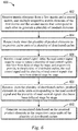
- Fig. 6 is a flowchart showing a method 600 for convolution operation according to an embodiment of the present disclosure. As shown in Fig. 6 , the method 600 includes blocks 602 to 610.
- the method 600 includes receiving matrix elements from a first matrix and from a second matrix, and multiplying matrix elements of the first matrix with corresponding matrix elements of the second matrix to generate a plurality of product elements.
- the method 600 includes respectively storing the plurality of product elements in respective cache units of a plurality of distributed caches.
- the method 600 includes receiving a read control signal, delaying the read control signal per stage to output a plurality of per-stage delayed read control signals, and respectively providing, to the plurality of distributed caches, the read control signal and the plurality of per-stage delayed read control signals.
- the method 600 includes receiving, from the plurality of distributed caches, product elements in cache units corresponding to the read control signal and the plurality of per-stage delayed read control signals.
- the method 600 includes generating accumulation data based on the received product elements in the respective cache units of the plurality of distributed caches.
- the method 600 may further include sequentially generating read control signals that correspond to the plurality of cache units of the plurality of distributed caches, respectively.
- storing the plurality of product elements includes: respectively storing, in each clock cycle of a plurality of clock cycles, the plurality of product elements in cache units of the plurality of distributed caches that correspond to clock cycle; and generating the read control signals includes: generating, in each clock cycle of a plurality of clock cycles, read control signals corresponding to the respective cache units of the plurality of distributed caches.
- storing the plurality of product elements includes: respectively and sequentially storing, in the respective cache units of the plurality of distributed caches, the plurality of product elements generated in each clock cycle; and generating the read control signals includes: generating, in each clock cycle of a plurality of clock cycles, the read control signals comprising a read address directed to one of the plurality of cache units, and adding one address unit to the read address in a next clock cycle.
- generating the accumulation data includes: generating the accumulation data based on product elements in cache units corresponding to the read address.
Landscapes
- Engineering & Computer Science (AREA)
- Physics & Mathematics (AREA)
- General Physics & Mathematics (AREA)
- Theoretical Computer Science (AREA)
- Mathematical Physics (AREA)
- Pure & Applied Mathematics (AREA)
- Computational Mathematics (AREA)
- Data Mining & Analysis (AREA)
- Mathematical Optimization (AREA)
- Mathematical Analysis (AREA)
- Computing Systems (AREA)
- General Engineering & Computer Science (AREA)
- Software Systems (AREA)
- Biophysics (AREA)
- Biomedical Technology (AREA)
- Life Sciences & Earth Sciences (AREA)
- Health & Medical Sciences (AREA)
- Databases & Information Systems (AREA)
- Algebra (AREA)
- Molecular Biology (AREA)
- General Health & Medical Sciences (AREA)
- Evolutionary Computation (AREA)
- Computational Linguistics (AREA)
- Artificial Intelligence (AREA)
- Neurology (AREA)
- Complex Calculations (AREA)
- Memory System Of A Hierarchy Structure (AREA)
Abstract
Description
- The present application claims priority to
Chinese Patent Application No. 201910977395.3 filed on October 15, 2019 - Embodiments of the present disclosure mainly relate to the field of data processing, and more specifically to an apparatus and a method for convolution operation.
- With the proposal and development of deep learning, convolutional neural networks have received increasing attention and have been developed. Convolution algorithm is the core algorithm of the convolutional neural network, and accounts for 90% of operation time of a convolutional neural network. Therefore, convolution operations are the primary optimization objects for designing a neural network hardware accelerator based on a field programmable gate array (FPGA). Hardware circuit design for convolution algorithm directly affects resource usage of the hardware accelerator and computing power that can be achieved.
- An adder tree structure, which is defined based on a convolution algorithm, is employed in one of conventional solutions. In the implementation of adder tree for convolution, six dimensions of convolution calculation are fully expanded based on a 6-layer loop characteristics of the convolution algorithm. To be specific, multiplication is first performed between corresponding points in a filter matrix and in an input data matrix, and then accumulation is performed per point within a window of the filter matrix and in the direction of a channel. This implementation is simple and straightforward. However, this implementation also has obvious shortcomings. If the dimension of computing is increased, the depth of an adder needs to be increased, and the amount of consumed resource increases exponentially, which is unacceptable for a resource-sensitive FPGA.
- According to embodiments of the present disclosure, an apparatus and a method for convolution operation with improved performance are provided.
- In a first aspect of the present disclosure, an apparatus for convolution operation is provided. The apparatus comprises: a plurality of multipliers configured to receive matrix elements from a first matrix and from a second matrix, respectively, and to generate a plurality of product elements, wherein each product element of the plurality of product element is obtained by multiplying, by a respective multiplier, a number of matrix elements of the first matrix and corresponding matrix elements of the second matrix; a plurality of distributed caches respectively coupled to the plurality of multipliers and each distributed cache of the plurality of distributed caches comprising a plurality of cache units, wherein the plurality of distributed caches is each configured to store a respective one of the plurality of product elements in a respective cache unit thereof; a register delay chain coupled to the plurality of distributed caches and comprising a plurality of registers coupled in series, wherein the register delay chain is configured to receive a read control signal, to delay the read control signal per stage to output a plurality of per-stage delayed read control signals, and to respectively provide, to the plurality of distributed caches, the read control signal and the plurality of per-stage delayed read control signals; and an accumulator circuit coupled to the plurality of distributed caches and configured to receive, from the plurality of distributed caches, product elements in cache units corresponding to the read control signal and the plurality of per-stage delayed read control signals, and to generate an accumulation data based on the received product elements in the respective cache units of the plurality of distributed caches.
- In a second aspect of the present disclosure, a method for convolution operation is provided. The method comprises: receiving matrix elements from a first matrix and from a second matrix, and multiplying matrix elements of the first matrix with corresponding matrix elements of the second matrix to generate a plurality of product elements; respectively storing the plurality of product elements in respective cache units of a plurality of distributed caches; receiving a read control signal, delaying the read control signal per stage to output a plurality of per-stage delayed read control signals, and respectively providing, to the plurality of distributed caches, the read control signal and the plurality of per-stage delayed read control signals; receiving, from the plurality of distributed caches, product elements in cache units corresponding to the read control signal and the plurality of per-stage delayed read control signals; and generating accumulation data based on the received product elements in the respective cache units of the plurality of distributed caches.
- It should be understood that the content described in the summary is not intended to limit critical or significant features of the embodiments of the present disclosure, nor is it intended to limit the scope of the present disclosure. Other features of the present disclosure will be easily comprehensible from the following description.
- The above and other features, advantages, and aspects of various embodiments of the present disclosure will become more apparent in conjunction with the drawings and with reference to the following detailed description. In the drawings, the same or similar reference numerals denote the same or similar elements. In the figures:
-
Fig. 1 is a schematic diagram showing a model for convolution operation; -
Fig. 2 is a block diagram showing an apparatus for convolution operation according to an embodiment of the present disclosure; -
Fig. 3 is a schematic diagram showing an apparatus for convolution operation according to an embodiment of the present disclosure; -
Fig. 4 is a schematic diagram showing matrix elements that are input in various clock cycles and product elements that are generated in the clock cycles according to an embodiment of the present disclosure; -
Fig. 5 is a schematic diagram showing product elements that are read in the clock cycles according to an embodiment of the present disclosure; and -
Fig. 6 is a flowchart showing a method for convolution operation according to an embodiment of the present disclosure. - Embodiments of the present disclosure will be described in more detail below with reference to the accompanying drawings. Although some embodiments of the present disclosure are shown in the accompanying drawings, it should be understood that the present disclosure can be implemented in various forms and should not be construed as being limited to the embodiments set forth herein. On the contrary, these embodiments are provided for a more thorough and complete understanding of the present disclosure. It should be understood that the accompanying drawings and the embodiments of the present disclosure are merely for illustrative purposes, and are not intended to limit the scope of protection of the present disclosure.
- In the description of the embodiments of the present disclosure, the term "comprise" and similar terms should be understood as non-exclusive inclusion, that is, "including but not limited to". The term "based on" should be understood as "at least partially based on". The terms "an embodiment" or "the embodiment" should be understood as "at least one embodiment". The terms "first", "second", and the like may refer to different or the same objects. Other explicit and implicit definitions may also be included below.
- Compared with the above-mentioned implementation of adder tree for convolution, in order to reduce the amount of resource to be used, a systolic array structure is used in another conventional solution. A systolic array implementation involves a spatially expansion of the five dimensions of a convolution calculation and a temporally expansion of the dimension of a channel. This solution can effectively utilize resources because when the dimensions of convolution calculation increases, resources required for the systolic array implementation do not need to be increased, but only the accumulation in the direction of the channel is extended in the time dimension. This conventional solution implements a delay chain in the dimension of the channel by using register resources in an FPGA. For example, in this conventional solution, registers are used to delay intermediate calculation data by six clock cycles before accumulation. However, such a solution also has a shortcoming that register resources are consumed excessively. FPGA overall resources usually comprise a lookup table (LUT), an LUT memory (LUTM), a register, and a digital signal processor (DSP). Excessive consumption of register resources will cause the unbalanced use of the FPGA overall resources, which leads to the "bucket effect".
- In order to solve at least the above-mentioned problems, the embodiments of the present disclosure provide a convolution operation solution that can save hardware resources and balance the required hardware resources. According to an embodiment of the present disclosure, a product of two corresponding matrix elements, each in one matrix, is stored in a respective cache unit of a plurality of distributed caches. A read control signal for the respective cache unit of the plurality of distributed caches is delayed per stage by a register delay chain. An accumulation result is generated based on products which are received from the plurality of distributed caches and which were stored in respective cache units corresponding to read control signals.
- In embodiments according to the present disclosure, by configuring a plurality of distributed caches and a register delay chain for read control signal for the plurality of distributed caches, a functionality similar to that of a register delay chain for intermediate calculation data in the systolic array structure is achieved, which facilitates the implementation of convolution operation. Therefore, the read control signal is delayed per stage while the products are maintained in the distributed caches, so as to prevent the transfer of intermediate calculation data by the register delay chain as in the systolic array structure. In this way, the convolution operation solution according to the embodiments of the present disclosure reduces overall power consumption while saving register resources. In some embodiments, utilizing distributed caches that are usually idle, such as LUTMs in an FPGA, can save overall design resources and achieve resource balancing.
- The present disclosure will be described in detail below in conjunction with the accompanying drawings and with reference to various embodiments.
-
Fig. 1 is a schematic diagram showing amodel 100 for convolution operation. As shown inFig. 1 , an input data set matrix comprises a plurality ofinput data matrices 102, and a filter set matrix comprises a plurality offilter matrices 104. Theinput data matrix 102 is a matrix of various data output by a sensor, and thefilter matrix 104 is a window matrix for performing a convolution operation. For example, annotation C shown inFig. 1 represents the number of channels ofinput data matrices 102 in the input data set matrix or the number of channels offilter matrices 104 in the filter set matrix. In addition, the dimensions of eachinput data matrix 102 are H × W, and the dimensions of eachfilter matrix 104 are R × S. - Referring to
Fig. 1 , convolution operations are performed on a plurality offilter matrices 104 in each filter set matrix and the plurality ofinput data matrices 102 in the input data set matrix, to generate oneoutput matrix 106. Therefore, when a plurality of filter set matrices are used for convolution operation, a plurality of output channels ofoutput matrices 106 are generated. For example, when M filter set matrices are used, M channels ofoutput matrices 106 are generated, and the dimensions of eachoutput matrix 106 are E × F. - In the convolution operation, performing a convolution operation on a
filter matrix 104 and a correspondinginput data matrix 102 at one window means multiplying matrix elements in a submatrix of theinput data matrix 102 that corresponds to the window by corresponding matrix elements of thefilter matrix 104 to generate product elements, and these product elements are summed up to generate an accumulation data. For example, as shown inFig. 1 , convolution operations are performed onC filter matrices 104 and Cinput data matrices 102 at the window shown to generate C pieces of accumulation data, and these C pieces of accumulation data are summed up to generate one matrix element in theoutput matrix 106. Matrix elements in theoutput matrix 106 are generated by shifting the window within theinput data matrix 102. Further, when M filter set matrices instead of one matrix are used,M output matrices 106 are generated as described above for use in calculation in following stages. - Hereinafter, a convolution operation on a plurality of
filter matrices 104 and the corresponding submatrices of a plurality ofinput data matrices 102 at one window will be taken as an example for description. -
Fig. 2 is a block diagram showing anapparatus 200 for convolution operation according to an embodiment of the present disclosure. As shown inFig. 2 , theapparatus 200 comprises a plurality ofmultipliers 202, a plurality of distributedcaches 204, aregister delay chain 206, and anaccumulator circuit 208. - The plurality of
multipliers 202 are configured to receive matrix elements from a first matrix and from a second matrix, respectively, and to generate a plurality of product elements, wherein each product element of the plurality of product element is obtained by multiplying, by a respective multiplier, a number of matrix elements of the first matrix and corresponding matrix elements of the second matrix. In some embodiments, the first matrix is an input data set matrix of input data matrices including a plurality of channels, and the second matrix is a filter set matrix of filter matrices including a plurality of channels. In some embodiments, in each clock cycle of a plurality of clock cycles, the plurality ofmultipliers 202 receive matrix elements and generate a plurality of product elements. In some embodiments, the input data set matrix includes input data matrices with C channels, the filter set matrix includes filter matrices with C channels. In each of the C clock cycles the plurality ofmultipliers 202 receive matrix elements of input data matrix from one channel and of filter matrix from one corresponding channel, and generate a plurality of product elements. - The plurality of distributed
caches 204 are respectively coupled to the plurality ofmultipliers 202 and each comprise a plurality of cache units. The plurality of distributedcaches 204 are each configured to store a respective one of the plurality of product elements in a respective cache unit thereof. In some embodiments, in each clock cycle of a plurality of clock cycles, the plurality of distributedcaches 204 receive a plurality of product elements from a plurality ofmultipliers 202, and store each of the plurality of product elements in a respective cache unit that correspond to the clock cycle in a respective one of the plurality of distributed caches, respectively. In some embodiments, in a plurality of clock cycles, each of the plurality of distributedcaches 204 sequentially stores a plurality of product elements in respective cache units thereof. - The
register delay chain 206 is coupled to the plurality of distributedcaches 204 and includes a plurality of registers coupled in series. Theregister delay chain 206 is configured to receive a read control signal, delay the read control signal per stage to output a plurality of per-stage delayed read control signals, and respectively provide, to the plurality of distributedcaches 204, the read control signal and the plurality of per-stage delayed read control signals. In some embodiments, in each clock cycle of a plurality of clock cycles, theregister delay chain 206 receives a read control signal which corresponds to a respective cache unit of each distributed cache. In some embodiments, in each of the plurality of clock cycles, a first distributed cache in the plurality of distributedcaches 204 receives an undelayed read control signal. In some embodiments, in each clock cycle of a plurality of clock cycles, each register in theregister delay chain 206 delays a read control signal received by the register, and provides, in a next clock cycle, the delayed read control signal to the corresponding cache unit and a register of the next stage. - The
accumulator circuit 208 is coupled to the plurality of distributedcaches 204. Theaccumulator circuit 208 is configured to receive, from the plurality of distributedcaches 204, product elements in cache units corresponding to the read control signal and the plurality of per-stage delayed read control signals, and to generate an accumulation data based on the received product elements in the respective cache units of the plurality of distributed caches. In some embodiments, in each clock cycle of a plurality of clock cycles, theaccumulator circuit 208 receives, from the plurality of distributedcaches 204, product elements in cache units corresponding to the read control signals received by the distributed caches. In some embodiments, theaccumulator circuit 208 accumulates product elements received from cache units of the plurality of distributedcaches 204 that correspond to the same clock cycle. In some embodiments, theaccumulator circuit 208 accumulates product elements generated in the same clock cycle. In some embodiments, when the input data set matrix includes input data matrices with C channels and the filter set matrix includes filter matrices with C channels, after C clock cycles, theaccumulator circuit 208 outputs a result of a convolution operation on one channel of input data matrix and one corresponding channel of filter matrix within a certain window, and after another clock cycle, theaccumulator circuit 208 outputs a result of a convolution operation on another channel of input data matrix and one corresponding channel of filter matrix within a certain window, and so on. - Referring to
Fig. 2 , in some embodiments, theapparatus 200 may further include a read controlsignal generation circuit 210. The read controlsignal generation circuit 210 is configured to sequentially generate read control signals that correspond to the plurality of cache units of the plurality of distributed caches, respectively 204. In some embodiments, in each clock cycle of a plurality of clock cycles, the read controlsignal generation circuit 210 generates read control signals corresponding to the respective cache units of the plurality of distributedcaches 204. In some embodiments, in each clock cycle of a plurality of clock cycles, the read controlsignal generation circuit 210 generates a read control signal that includes a read address for one of the plurality of cache units, and increase the read address by one address unit in a next clock cycle. In some embodiments, the read address corresponds to a cache unit, a clock cycle phase, and a product element generated in the clock cycle. - In some embodiments, in response to receiving, by each of the plurality of distributed
caches 204, the read control signal and the plurality of per-stage delayed read control signals, the plurality of distributedcaches 204 output, to theaccumulator circuit 208, product elements in cache units corresponding to the read address in the read control signal. - According to embodiments of the present disclosure, by configuring a plurality of distributed caches and a register delay chain for read control signals for the plurality of distributed caches, the read control signal are delayed per stage while the products are maintained in the distributed caches, so as to prevent the transfer of intermediate calculation data by the register delay chain as in the systolic array structure. In this way, an
apparatus 200 according to embodiments of the present disclosure reduces overall power consumption while saving register resources. - In some embodiments, the
apparatus 200 is included in an FPGA. In an alternative embodiment, theapparatus 200 is included in an application-specific integrated circuit. - In some embodiments, each distributed cache is an LUTM resource in the FPGA. For example, the FGPA is a Xilinx FPGA. In this way, a usually idle LUTM in the FPGA is used as the distributed cache, such that overall design resources are saved and resource balancing is achieved. In addition, because the LUTM is easily operated and does not involve complex control logic, a higher design dominant frequency can be supported, and the overall computing power of a neural network accelerator can be improved.
-
Fig. 3 is a schematic diagram showing anapparatus 300 for convolution operation according to an embodiment of the present disclosure. Theapparatus 300 ofFig. 3 includes a plurality ofmultipliers 202, a plurality of distributedcaches 204, aregister delay chain 206, and anaccumulator circuit 208. Theapparatus 300 may be considered as an implementation of theapparatus 200. It should be understood that for simplicity of illustration,Fig. 3 shows a read control signal ADDR_n without illustrating the configuration of any read controlsignal generation circuit 210 . The read controlsignal generation circuit 210 can be implemented by any circuit known to the art. - Referring to
Fig. 3 , the plurality ofmultipliers 202 includes multipliers M0 to M15, the plurality of distributedcaches 204 includes distributed caches LUTMO to LUTM15, theregister delay chain 206 includes a plurality of registers reg1 to reg15, and theaccumulator circuit 208 includes a multiplexer MUL module and accumulators ACC0 to ACC15. In addition, matrix elements w0 to w15 of a filter matrix are input to the multipliers M0 to M15, respectively, and the corresponding matrix elements i0 to i15 of an input data matrix are input to the multipliers M0 to M15, respectively. In addition, the distributed caches LUTM0 to LUTM15 each include a plurality of cache units Data0 to Data15. It should be understood that althoughFig. 3 shows the number of various components, theapparatus 300 according to this embodiment of the present disclosure may include any other number of various components. - In some embodiments, the number of multipliers M0 to M15 is equal to the number of matrix elements in the filter matrix. In some embodiments, the number of distributed caches LUTM0 to LUTM15 is equal to the number of matrix elements in the filter matrix. In some embodiments, the number of cache units Data0 to Data15 of each of the distributed caches LUTM0 to LUTM15 is equal to the number of channels of filter matrices. In some embodiments, the number of accumulators ACC0 to ACC15 is equal to the number of cache units Data0 to Data15. In some embodiments, the number of registers reg1 to reg15 is less than the number of distributed caches LUTM0 to LUTM15 by a predetermined value. For example, the determined value is 1. As an example, in
Fig. 3 , the number R × S of matrix elements of the filter matrix is equal to 16, and the number C of channels of filter matrices is equal to 16. - Referring to
Fig. 3 , the multipliers M0 to M15 are coupled to the distributed caches LUTM0 to LUTM15, respectively. The registers reg1 to reg15 are coupled in series with each other to form a delay chain, the register reg1 receives the read control signal ADDR_n as an input to the delay chain, and outputs of the registers reg1 to regl5 are coupled to the distributed caches LUTM1 to LUTM15, respectively. The distributed caches LUTM0 to LUTM15 are coupled to the multiplexer MUL module. In some embodiments, each of the distributed caches LUTM0 to LUTM15 is a ring cache. The multiplexer MUL module is coupled to the accumulators ACC0 to ACC15. Each accumulator includes an adder and a register, the output of the adder being coupled to the register while the output of the register being coupled to the adder as one input of the adder to achieve accumulation. Each of the outputs of the multiplexer MUL module is coupled to the other input of a corresponding adder. The accumulator ACC0 includes an adder dsp0 and a register Reg0. The accumulator ACC1 includes an adder dsp1 and a register Reg1. Analogously, the accumulator ACC15 includes an adder dsp15 and a register Reg15. - Operations of the
apparatus 300 for convolution operation shown inFig. 3 will be described below in conjunction withFigs. 4 and 5. Fig. 4 is a schematic diagram showing matrix elements that are input in various clock cycles and product elements that are generated in the clock cycles according to an embodiment of the present disclosure.Fig. 5 is a schematic diagram showing product elements that are read in the respective clock cycles according to an embodiment of the present disclosure. - Referring to
Figs. 3 and4 , the multipliers M0 to M15 receive the matrix elements w0 to w15 and the matrix elements i0 to i15 in each clock cycle of a plurality of clock cycles clock0 to clock15, to generate product elements wo*i0 to w15*i15. In each of the plurality of clock cycles clock0 to clock15, each of the distributed caches LUTM0 to LUTM15 store a respective one of product elements wo*i0 to w15*i15 in a respective cache unit, which corresponds to the present clock cycle, of cache units Data0 to Data15 in the distributed caches, respectively. As an example, each the distributed caches LUTM0 to LUTM15 stores, in a cache unit Data0 thereof, a respective one of product elements wo*i0 to w15*i15 generated in clock cycle clock0. Further, each of the distributed caches LUTM0 to LUTM15 stores, in a cache unit Data1 thereof, a respective one of product elements wo*i0 to w15*i15 generated in clock cycle clock1. Analogously, each of the distributed caches LUTM0 to LUTM15 stores, in a cache units Data15 thereof, a respective one of product elements wo*i0 to w15*i15 generated in clock cycle clockl5. - It is shown in
Fig. 4 that the product elements wo*i0 to w15*i15 are generated in a clock cycle clockl16. The 17th clock cycle clock16 may be considered as the start of a cycle of a convolution operation on the filter matrix and the input data matrix after the filter matrix is shifted to a next window position. - Referring to
Figs. 3 and4 , a read control signal ADDR_n is generated in each of the plurality of clock cycles clock0 to clock15, where n is less than or equal to 0 and greater than or equal to 15. As an example, a read control signal ADDR_0 is generated in clock cycle clock0, which corresponds to a cache unit Data0 and is used for reading a respective product element in cache unit Data0 of a respective distributed cache, and a read control signal ADDR_1 is generated in clock cycle clock1, which corresponds to cache unit Data1 and is used for reading a respective product element in a cache unit Data1 of a respective distributed cache. Analogously, a read control signal ADDR_15 is generated in clock cycle clock15, which corresponds to cache unit Data15 and is used for reading a respective product element in a cache unit Data15 of a respective distributed cache. - Referring to
Figs. 3 and5 , the read control signal ADDR_0 generated in clock cycle clock0 is provided to the distributed cache LUTM0, and the product element wo*i0 in the cache unit Data0 of the distributed cache LUTM0 is read in clock cycle clock0. The read control signal ADDR_0 generated in clock cycle clock0 is input to the register reg1, and the register reg1 delays the read control signal ADDR_0. In other words, the register reg1 stores the read control signal ADDR_0 in clock cycle clock0, and outputs the read control signal ADDR_0 in the next clock cycle clock1. The register regl provides the delayed read control signal ADDR_0 to the distributed cache LUTM1 in the next clock cycle clock1, and the product element w1*il in the cache unit Data0 of the distributed cache LUTM1 is read in clock cycle clock1. In addition, the read control signal ADDR_1 generated in clock cycle clock1 is provided to the distributed cache LUTM0, and the product element wo*i0 in the cache unit Data1 of the distributed cache LUTM0 is read in clock cycle clockl. In addition, in clock cycle clock1, the read control signal ADDR_0 is input to the register reg2, and the register reg2 delays the read control signal ADDR_0; the read control signal ADDR_1 is input to the register reg1, and the register reg1 delays the read control signal ADDR_1. - Analogously, in clock cycle clock2, the product element w2*i2 in the cache unit Data0 of the distributed cache LUTM2, the product element w1*i1 in the cache unit Data1 of the distributed cache LUTM1, and the product element w0*i0 in the cache unit Data2 of the distributed cache LUTM0 are read. In addition, in clock cycle clockl5, the product element w15*i15 in the cache unit Data0 of the distributed cache 5, the product element w14*i14 in the cache unit Data1 of the distributed cache LUTM14, ..., and the product element w0*i0 in the cache unit Data15 of the distributed cache LUTM0 are read.
Fig. 3 shows a respective product element in a cache unit Data15, Data14, ..., Data0 that are received by the multiplexer MUL module in clock cycle clockl5. - Referring to
Figs. 3 and5 , in clock cycle clock0, the multiplexer MUL module receives the product element wo*i0 in the cache unit Data0 of the distributed cache LUTM0, and provides the product element wo*i0 to the accumulator ACC0 corresponding to the cache unit Data0. In clock cycle clock0, the adder dsp0 in the accumulator ACC0 adds up the product element wo*i0 and null data, and stores an accumulation result in the register Reg0. In clock cycle clock1, the multiplexer MUL module receives the product element w1*i1 in the cache unit Data0 of the distributed cache LUTM1 and the product element wo*i0 in the cache unit Data1 of the distributed cache LUTM0, provides the product element w1*i1 in the cache unit Data0 of the distributed cache LUTM1 to the accumulator ACC0 corresponding to the cache unit Data0, and provides the product element wo*i0 in the cache unit Data1 of the distributed cache LUTM0 to the accumulator ACC1 corresponding to the cache unit Data1. In clock cycle clock1, the adder dsp0 in the accumulator ACC0 adds up the product element w1*i1 and the accumulation data generated in clock cycle clock0, and stores new accumulation data in the register Reg0, and the adder dsp1 in the accumulator ACC1 adds up the product element wo*i0 and null data, and stores an accumulation result in the register Reg1. - Analogously, in clock cycle clockl5, the adder dsp0 in the accumulator ACC0 adds up the product element w15*i15 and the accumulation data generated in clock cycle clock14, and stores new accumulation data in the register Reg0. In this way, the sum of a respective product element w0*i0 to w15*i15 generated in clock cycle clock0, that is, the result of the convolution operation, is obtained. In clock cycle clock16 after the 16 clock cycles, the accumulator ACC0 outputs the result of the convolution operation on the respective matrix elements of the two matrices that are input in clock cycle clock0. In addition, in clock cycle cloc16, the adder dsp1 in the accumulator ACC1 adds up the product element w15*i15 and the accumulation data generated in clock cycle clock15, and stores new accumulation data in the register Reg1. In this way, the sum of a respective product element w0*i0 to w15*i15 generated in clock cycle clock1, that is, the result of the convolution operation, is obtained. In clock cycle clock17 after the 17 clock cycles, the accumulator ACC1 outputs the result of the convolution operation on the respective matrix elements of the two matrices that are input in clock cycle clock1, and so on.
- Referring to
Fig. 5 , the accumulators ACC0 to ACC15 each accumulate a respective product element of the respective cache units that are read by a delay of one clock cycle with each other, that is, accumulate a respective product element on the diagonal lines shown in the figure to respectively generate a result of a convolution operation corresponding to a clock cycle in which a respective product element are generated. - According to this embodiment of the present disclosure, a convolution operation is implemented by configuring a plurality of distributed caches and a register delay chain for read control signal for the plurality of distributed caches. The read control signal is delayed per stage while the products are maintained in the distributed caches, so as to prevent the transfer of intermediate calculation data by the register delay chain as in the systolic array structure. In this way, the apparatus for convolution operation according to this embodiment of the present disclosure reduces overall power consumption while saving register resources. Further, utilizing distributed caches that are usually idle, such as LUTMs in an FPGA, can save overall design resources and achieve resource balancing.
-
Fig. 6 is a flowchart showing amethod 600 for convolution operation according to an embodiment of the present disclosure. As shown inFig. 6 , themethod 600 includesblocks 602 to 610. - At
block 602, themethod 600 includes receiving matrix elements from a first matrix and from a second matrix, and multiplying matrix elements of the first matrix with corresponding matrix elements of the second matrix to generate a plurality of product elements. - At
block 604, themethod 600 includes respectively storing the plurality of product elements in respective cache units of a plurality of distributed caches. - At
block 606, themethod 600 includes receiving a read control signal, delaying the read control signal per stage to output a plurality of per-stage delayed read control signals, and respectively providing, to the plurality of distributed caches, the read control signal and the plurality of per-stage delayed read control signals. - At
block 608, themethod 600 includes receiving, from the plurality of distributed caches, product elements in cache units corresponding to the read control signal and the plurality of per-stage delayed read control signals. - At
block 610, themethod 600 includes generating accumulation data based on the received product elements in the respective cache units of the plurality of distributed caches. - In some embodiments, the
method 600 may further include sequentially generating read control signals that correspond to the plurality of cache units of the plurality of distributed caches, respectively. - In some embodiments, storing the plurality of product elements includes: respectively storing, in each clock cycle of a plurality of clock cycles, the plurality of product elements in cache units of the plurality of distributed caches that correspond to clock cycle; and generating the read control signals includes: generating, in each clock cycle of a plurality of clock cycles, read control signals corresponding to the respective cache units of the plurality of distributed caches.
- In some embodiments, storing the plurality of product elements includes: respectively and sequentially storing, in the respective cache units of the plurality of distributed caches, the plurality of product elements generated in each clock cycle; and generating the read control signals includes: generating, in each clock cycle of a plurality of clock cycles, the read control signals comprising a read address directed to one of the plurality of cache units, and adding one address unit to the read address in a next clock cycle.
- In some embodiments, generating the accumulation data includes: generating the accumulation data based on product elements in cache units corresponding to the read address.
- It should be understood that the method for implementing this embodiment of the present disclosure can be written in any combination of one or more programming languages, to adapt to a system-on-chip (SoC) architecture. In addition, although the various operations are depicted in a order, it should be understood as requiring such operations to be performed in the order shown or in a sequential order, or requiring all illustrated operations to be performed to achieve desired results. Under certain circumstances, multitasking and parallel processing may be advantageous.
- Although details of several implementations are included in the foregoing discussions, these details should not be construed as limiting the scope of the present disclosure. Some features that are described in the context of separate embodiments can also be implemented in combination in a single implementation. In contrast, various features described in the context of a single implementation may alternatively be implemented in a plurality of implementations individually or in any suitable subcombination.
- Although the subject matter has been described in languages specific to structural features and/or logical actions of the method, it should be understood that the subject matter defined in the appended claims is not necessarily limited to the features or actions described above. On the contrary, the features and actions described above are merely exemplary forms for implementing the claims.
Claims (20)
- An apparatus for convolution operation, comprising:a plurality of multipliers configured to receive matrix elements from a first matrix and from a second matrix, respectively, and to generate a plurality of product elements, wherein each product element of the plurality of product element is obtained by multiplying, by a respective multiplier, a number of matrix elements of the first matrix and corresponding matrix elements of the second matrix;a plurality of distributed caches respectively coupled to the plurality of multipliers and each distributed cache of the plurality of distributed caches comprising a plurality of cache units, wherein the plurality of distributed caches is each configured to store a respective one of the plurality of product elements in a respective cache unit thereof;a register delay chain coupled to the plurality of distributed caches and comprising a plurality of registers coupled in series, wherein the register delay chain is configured to receive a read control signal, to delay the read control signal per stage to output a plurality of per-stage delayed read control signals, and to provide the read control signal and the plurality of per-stage delayed read control signals to the plurality of distributed caches, respectively; andan accumulator circuit coupled to the plurality of distributed caches and configured to receive, from the plurality of distributed caches, product elements in cache units corresponding to the read control signal and the plurality of per-stage delayed read control signals, and to generate accumulation data based on the received product elements in the respective cache units of the plurality of distributed caches.
- The apparatus according to claim 1, wherein the accumulator circuit comprises:a multiplexer module coupled to the plurality of distributed caches and configured to receive the product elements in the cache units corresponding to the read control signal and the plurality of per-stage delayed read control signals; anda plurality of accumulators, each accumulator of the plurality of accumulators being coupled to the multiplexer module and being configured to receive, from the multiplexer module, product elements in cache units of the plurality of distributed caches that correspond to the accumulator, and the plurality of accumulators being configured to generate the accumulation data based on the received product elements.
- The apparatus according to claim 2, wherein the number of the plurality of accumulators is equal to the number of the plurality of cache units of each distributed cache of the plurality of distributed caches.
- The apparatus according to claim 1, further comprising:
a read control signal generation circuit configured to sequentially generate read control signals that correspond to the plurality of cache units of the plurality of distributed caches, respectively. - The apparatus according to claim 4, whereinthe plurality of distributed caches is configured to store, in each clock cycle of a plurality of clock cycles, the plurality of product elements in cache units of the plurality of distributed caches that correspond to the clock cycle; andthe read control signal generation circuit is configured to generate, in each clock cycle of a plurality of clock cycles, a read control signal corresponding to a respective cache unit of each distributed cache of the plurality of distributed caches.
- The apparatus according to claim 5, wherein each of the plurality of distributed caches is configured to store, in respective cache units thereof, the plurality of product elements generated in the respective clock cycle sequentially; and
the read control signal generation circuit is configured to generate, in each clock cycle of a plurality of clock cycles, the read control signals comprising a read address directed to one of the plurality of cache units, and add one address unit to the read address in a next clock cycle. - The apparatus according to claim 6, wherein each of the plurality of distributed caches is configured to output, to the accumulator circuit, a product element in a cache unit corresponding to the read address.
- The apparatus according to claim 1, wherein the apparatus is comprised in a field-programmable gate array.
- The apparatus according to claim 8, wherein each of the plurality of distributed caches is a lookup table memory (LUTM).
- The apparatus according to claim 1, wherein the apparatus is comprised in an application-specific integrated circuit.
- The apparatus according to any one of claims 1 to 10, wherein the first matrix is an input data set matrix, and the second matrix is a filter set matrix;wherein the input data set matrix comprises input data matrices with a number of channels, and the filter set matrix comprises filter matrices with a number of channels, andwherein the number of channels of the input data matrices is equal to the number of channels of the filter matrices.
- The apparatus according to claim 11, wherein the number of the plurality of cache units of each distributed cache of the plurality of distributed caches is equal to the number of channels of the filter matrices.
- The apparatus according to claim 11, wherein in each clock cycle of a plurality of clock cycles, matrix elements in one channel of a filter matrix and corresponding matrix elements in one corresponding channel of an input data matrix are input to the plurality of multipliers, respectively.
- The apparatus according to claim 11, wherein the number of the plurality of distributed caches is equal to the number of matrix elements of the filter matrix.
- The apparatus according to claim 14, wherein the number of the plurality of registers is less than, by a predetermined value, the number of the plurality of distributed caches.
- A method for convolution operation, comprising:receiving matrix elements from a first matrix and from a second matrix, and multiplying matrix elements of the first matrix with corresponding matrix elements of the second matrix to generate a plurality of product elements;storing, each of the plurality of product elements, in a respective cache unit of the plurality of distributed caches;receiving a read control signal, delaying the read control signal per stage to output a plurality of per-stage delayed read control signals, and providing, to the plurality of distributed caches respectively, the read control signal and the plurality of per-stage delayed read control signals;receiving, from the plurality of distributed caches, product elements in cache units corresponding to the read control signal and the plurality of per-stage delayed read control signals; andgenerating accumulation data based on the received product elements in the respective cache units of the plurality of distributed caches.
- The method according to claim 16, further comprising:
generating read control signals, each corresponding to a respective cache unit of the plurality of distributed caches, sequentially. - The method according to claim 17, whereinstoring the plurality of product elements comprises: storing, in each clock cycle of a plurality of clock cycles, each of the plurality of product elements in a cache unit that corresponds to the clock cycle of a respective one of the plurality of distributed caches; andgenerating the read control signals comprises: generating, in each clock cycle of a plurality of clock cycles, read control signals each corresponding to a respective cache unit of the plurality of distributed caches.
- The method according to claim 18, whereinstoring the plurality of product elements comprises: storing each of the plurality of product elements generated in each of the plurality clock cycles in a respective cache unit of the plurality of distributed caches sequentially; andgenerating the read control signals comprises: generating, in each clock cycle of a plurality of clock cycles, the read control signals comprising a read address for one of the plurality of cache units, and increasing the read address by one address unit in a next clock cycle.
- The method according to claim 19, wherein
generating the accumulation data comprises: generating the accumulation data based on product elements in cache units corresponding to the read address.
Applications Claiming Priority (2)
| Application Number | Priority Date | Filing Date | Title |
|---|---|---|---|
| CN201910977395.3A CN110717588B (en) | 2019-10-15 | 2019-10-15 | Apparatus and method for convolution operation |
| PCT/CN2020/083574 WO2021073053A1 (en) | 2019-10-15 | 2020-04-07 | Device and method for convolution operation |
Publications (3)
| Publication Number | Publication Date |
|---|---|
| EP3893166A1 true EP3893166A1 (en) | 2021-10-13 |
| EP3893166A4 EP3893166A4 (en) | 2022-11-30 |
| EP3893166B1 EP3893166B1 (en) | 2024-08-14 |
Family
ID=69211698
Family Applications (1)
| Application Number | Title | Priority Date | Filing Date |
|---|---|---|---|
| EP20876067.8A Active EP3893166B1 (en) | 2019-10-15 | 2020-04-07 | Device and method for convolution operation |
Country Status (5)
| Country | Link |
|---|---|
| US (1) | US11556614B2 (en) |
| EP (1) | EP3893166B1 (en) |
| JP (1) | JP7244660B2 (en) |
| CN (1) | CN110717588B (en) |
| WO (1) | WO2021073053A1 (en) |
Families Citing this family (3)
| Publication number | Priority date | Publication date | Assignee | Title |
|---|---|---|---|---|
| CN110717588B (en) | 2019-10-15 | 2022-05-03 | 阿波罗智能技术(北京)有限公司 | Apparatus and method for convolution operation |
| CN112580787B (en) | 2020-12-25 | 2023-11-17 | 北京百度网讯科技有限公司 | Data processing method, device, equipment and storage medium for neural network accelerator |
| CN115906930B (en) * | 2021-09-29 | 2026-03-24 | Oppo广东移动通信有限公司 | A neural network acceleration method, accelerator, electronic device, and storage medium |
Family Cites Families (24)
| Publication number | Priority date | Publication date | Assignee | Title |
|---|---|---|---|---|
| JPH03201817A (en) * | 1989-12-28 | 1991-09-03 | Sony Corp | Digital filter and inner product calculating circuit |
| JP2945487B2 (en) * | 1990-12-26 | 1999-09-06 | 株式会社日立製作所 | Matrix multiplier |
| JP4442644B2 (en) * | 2007-06-15 | 2010-03-31 | 株式会社デンソー | Pipeline arithmetic unit |
| US8117247B1 (en) * | 2007-07-19 | 2012-02-14 | Xilinx, Inc. | Configurable arithmetic block and method of implementing arithmetic functions in a device having programmable logic |
| CN104915322B (en) * | 2015-06-09 | 2018-05-01 | 中国人民解放军国防科学技术大学 | A kind of hardware-accelerated method of convolutional neural networks |
| CN106485319B (en) * | 2015-10-08 | 2019-02-12 | 上海兆芯集成电路有限公司 | Neural network units with neural processing units dynamically configurable to execute on multiple data sizes |
| JP6700712B2 (en) * | 2015-10-21 | 2020-05-27 | キヤノン株式会社 | Convolution operation device |
| CN106127302A (en) * | 2016-06-23 | 2016-11-16 | 杭州华为数字技术有限公司 | Process the circuit of data, image processing system, the method and apparatus of process data |
| KR102868989B1 (en) * | 2016-11-28 | 2025-10-10 | 삼성전자주식회사 | Convolution processing apparatus and method |
| CN106844294B (en) * | 2016-12-29 | 2019-05-03 | 华为机器有限公司 | Convolution arithmetic chips and communication equipment |
| CN106940815B (en) * | 2017-02-13 | 2020-07-28 | 西安交通大学 | A Programmable Convolutional Neural Network Coprocessor IP Core |
| CN107301455B (en) * | 2017-05-05 | 2020-11-03 | 中国科学院计算技术研究所 | Hybrid cube storage system for convolutional neural network and accelerated computing method |
| US11775313B2 (en) * | 2017-05-26 | 2023-10-03 | Purdue Research Foundation | Hardware accelerator for convolutional neural networks and method of operation thereof |
| CN108804139B (en) * | 2017-06-16 | 2020-10-20 | 上海兆芯集成电路有限公司 | Programmable device, method of operation thereof, and computer usable medium |
| CN108805276B (en) * | 2017-06-16 | 2020-09-22 | 上海兆芯集成电路有限公司 | Processor, method for operating processor and computer usable medium |
| US10671349B2 (en) | 2017-07-24 | 2020-06-02 | Tesla, Inc. | Accelerated mathematical engine |
| CN109993272B (en) * | 2017-12-29 | 2019-12-06 | 北京中科寒武纪科技有限公司 | convolution and down-sampling operation unit, neural network operation unit and field programmable gate array integrated circuit |
| CN110210610B (en) * | 2018-03-27 | 2023-06-20 | 腾讯科技(深圳)有限公司 | Convolution computing accelerator, convolution computing method, and convolution computing device |
| US11216532B2 (en) | 2018-09-26 | 2022-01-04 | Intel Corporation | Circuitry for high-bandwidth, low-latency machine learning |
| CN109784489B (en) * | 2019-01-16 | 2021-07-30 | 北京大学软件与微电子学院 | Convolutional neural network IP core based on FPGA |
| CN110135554A (en) * | 2019-03-25 | 2019-08-16 | 电子科技大学 | An FPGA-based Convolutional Neural Network Hardware Acceleration Architecture |
| CN110175670B (en) * | 2019-04-09 | 2020-12-08 | 华中科技大学 | A method and system for implementing YOLOv2 detection network based on FPGA |
| CN110070178B (en) * | 2019-04-25 | 2021-05-14 | 北京交通大学 | Convolutional neural network computing device and method |
| CN110717588B (en) * | 2019-10-15 | 2022-05-03 | 阿波罗智能技术(北京)有限公司 | Apparatus and method for convolution operation |
-
2019
- 2019-10-15 CN CN201910977395.3A patent/CN110717588B/en active Active
-
2020
- 2020-04-07 WO PCT/CN2020/083574 patent/WO2021073053A1/en not_active Ceased
- 2020-04-07 JP JP2021545885A patent/JP7244660B2/en active Active
- 2020-04-07 EP EP20876067.8A patent/EP3893166B1/en active Active
-
2022
- 2022-03-17 US US17/697,917 patent/US11556614B2/en active Active
Also Published As
| Publication number | Publication date |
|---|---|
| US20220207106A1 (en) | 2022-06-30 |
| US11556614B2 (en) | 2023-01-17 |
| WO2021073053A1 (en) | 2021-04-22 |
| CN110717588A (en) | 2020-01-21 |
| JP2022519314A (en) | 2022-03-22 |
| EP3893166B1 (en) | 2024-08-14 |
| JP7244660B2 (en) | 2023-03-22 |
| EP3893166A4 (en) | 2022-11-30 |
| CN110717588B (en) | 2022-05-03 |
Similar Documents
| Publication | Publication Date | Title |
|---|---|---|
| US11556614B2 (en) | Apparatus and method for convolution operation | |
| US20230359497A1 (en) | Electronic device and method for accelerating neural network computations | |
| CN108446761A (en) | A kind of neural network accelerator and data processing method | |
| US20150074443A1 (en) | Method and apparatus for asynchronous processor with fast and slow mode | |
| JP5356537B2 (en) | Digital signal processing block with pre-adder stage | |
| Pohokar et al. | Design and implementation of 16× 16 multiplier using Vedic mathematics | |
| CN113298245B (en) | Multi-precision neural network computing device and method based on data flow architecture | |
| US11593907B2 (en) | System and methods for computing 2-D convolutions and cross-correlations | |
| CN104679474A (en) | Multiplying unit on finite field GF (2 227) and modular multiplication algorithm | |
| CN104579240A (en) | FPGA-based configurable-coefficient filter and filtering method, and electronic equipment | |
| US9552328B2 (en) | Reconfigurable integrated circuit device | |
| Takizawa et al. | A design support tool set for asynchronous circuits with bundled-data implementation on FPGAs | |
| US20260010346A1 (en) | Nature exponential function computing device and computing method thereof | |
| Das et al. | Hardware implementation of parallel FIR filter using modified distributed arithmetic | |
| Poudereux et al. | Design of a filter bank multi-carrier system for broadband power line communications | |
| KR100249040B1 (en) | Fir filter having asymmetric frequency response characteristic | |
| US10410700B1 (en) | Systems and method for a low-power correlator architecture using shifting coefficients | |
| EP2296093A2 (en) | DSP execution unit for efficient alternate modes of operation | |
| Dai et al. | APIR-DSP: An approximate PIR-DSP architecture for error-tolerant applications | |
| CN115618177A (en) | Hardware Acceleration System of Covariance Matrix Operation Based on State Machine | |
| Lakshmi et al. | Efficient FPGA implementation of the delayed LMS algorithm | |
| Dai et al. | An Efficient Spiking Convolutional Architecture with Compressed Address Event Representation and Adaptive Delay Asynchronous Clocks | |
| Mankar et al. | Design and Verification of low power DA-Adaptive digital FIR filter | |
| Kumaar et al. | An Efficient Ripple Carry Adder Using Pipelining | |
| CN112800387B (en) | Radix-6 butterfly operation unit, method, electronic device and storage medium |
Legal Events
| Date | Code | Title | Description |
|---|---|---|---|
| STAA | Information on the status of an ep patent application or granted ep patent |
Free format text: STATUS: THE INTERNATIONAL PUBLICATION HAS BEEN MADE |
|
| PUAI | Public reference made under article 153(3) epc to a published international application that has entered the european phase |
Free format text: ORIGINAL CODE: 0009012 |
|
| STAA | Information on the status of an ep patent application or granted ep patent |
Free format text: STATUS: REQUEST FOR EXAMINATION WAS MADE |
|
| 17P | Request for examination filed |
Effective date: 20210709 |
|
| AK | Designated contracting states |
Kind code of ref document: A1 Designated state(s): AL AT BE BG CH CY CZ DE DK EE ES FI FR GB GR HR HU IE IS IT LI LT LU LV MC MK MT NL NO PL PT RO RS SE SI SK SM TR |
|
| A4 | Supplementary search report drawn up and despatched |
Effective date: 20221031 |
|
| RIC1 | Information provided on ipc code assigned before grant |
Ipc: G06F 17/16 20060101ALI20221025BHEP Ipc: G06F 7/544 20060101ALI20221025BHEP Ipc: G06N 3/063 20060101AFI20221025BHEP |
|
| DAV | Request for validation of the european patent (deleted) | ||
| DAX | Request for extension of the european patent (deleted) | ||
| STAA | Information on the status of an ep patent application or granted ep patent |
Free format text: STATUS: EXAMINATION IS IN PROGRESS |
|
| 17Q | First examination report despatched |
Effective date: 20230829 |
|
| GRAP | Despatch of communication of intention to grant a patent |
Free format text: ORIGINAL CODE: EPIDOSNIGR1 |
|
| STAA | Information on the status of an ep patent application or granted ep patent |
Free format text: STATUS: GRANT OF PATENT IS INTENDED |
|
| INTG | Intention to grant announced |
Effective date: 20240307 |
|
| P01 | Opt-out of the competence of the unified patent court (upc) registered |
Effective date: 20240424 |
|
| GRAS | Grant fee paid |
Free format text: ORIGINAL CODE: EPIDOSNIGR3 |
|
| GRAA | (expected) grant |
Free format text: ORIGINAL CODE: 0009210 |
|
| STAA | Information on the status of an ep patent application or granted ep patent |
Free format text: STATUS: THE PATENT HAS BEEN GRANTED |
|
| AK | Designated contracting states |
Kind code of ref document: B1 Designated state(s): AL AT BE BG CH CY CZ DE DK EE ES FI FR GB GR HR HU IE IS IT LI LT LU LV MC MK MT NL NO PL PT RO RS SE SI SK SM TR |
|
| REG | Reference to a national code |
Ref country code: GB Ref legal event code: FG4D |
|
| REG | Reference to a national code |
Ref country code: CH Ref legal event code: EP |
|
| REG | Reference to a national code |
Ref country code: DE Ref legal event code: R096 Ref document number: 602020035954 Country of ref document: DE |
|
| REG | Reference to a national code |
Ref country code: IE Ref legal event code: FG4D |
|
| REG | Reference to a national code |
Ref country code: LT Ref legal event code: MG9D |
|
| REG | Reference to a national code |
Ref country code: NL Ref legal event code: MP Effective date: 20240814 |
|
| PG25 | Lapsed in a contracting state [announced via postgrant information from national office to epo] |
Ref country code: NO Free format text: LAPSE BECAUSE OF FAILURE TO SUBMIT A TRANSLATION OF THE DESCRIPTION OR TO PAY THE FEE WITHIN THE PRESCRIBED TIME-LIMIT Effective date: 20241114 |
|
| REG | Reference to a national code |
Ref country code: AT Ref legal event code: MK05 Ref document number: 1713995 Country of ref document: AT Kind code of ref document: T Effective date: 20240814 |
|
| PG25 | Lapsed in a contracting state [announced via postgrant information from national office to epo] |
Ref country code: FI Free format text: LAPSE BECAUSE OF FAILURE TO SUBMIT A TRANSLATION OF THE DESCRIPTION OR TO PAY THE FEE WITHIN THE PRESCRIBED TIME-LIMIT Effective date: 20240814 Ref country code: NL Free format text: LAPSE BECAUSE OF FAILURE TO SUBMIT A TRANSLATION OF THE DESCRIPTION OR TO PAY THE FEE WITHIN THE PRESCRIBED TIME-LIMIT Effective date: 20240814 Ref country code: GR Free format text: LAPSE BECAUSE OF FAILURE TO SUBMIT A TRANSLATION OF THE DESCRIPTION OR TO PAY THE FEE WITHIN THE PRESCRIBED TIME-LIMIT Effective date: 20241115 Ref country code: PL Free format text: LAPSE BECAUSE OF FAILURE TO SUBMIT A TRANSLATION OF THE DESCRIPTION OR TO PAY THE FEE WITHIN THE PRESCRIBED TIME-LIMIT Effective date: 20240814 Ref country code: PT Free format text: LAPSE BECAUSE OF FAILURE TO SUBMIT A TRANSLATION OF THE DESCRIPTION OR TO PAY THE FEE WITHIN THE PRESCRIBED TIME-LIMIT Effective date: 20241216 |
|
| PG25 | Lapsed in a contracting state [announced via postgrant information from national office to epo] |
Ref country code: BG Free format text: LAPSE BECAUSE OF FAILURE TO SUBMIT A TRANSLATION OF THE DESCRIPTION OR TO PAY THE FEE WITHIN THE PRESCRIBED TIME-LIMIT Effective date: 20240814 |
|
| PG25 | Lapsed in a contracting state [announced via postgrant information from national office to epo] |
Ref country code: LV Free format text: LAPSE BECAUSE OF FAILURE TO SUBMIT A TRANSLATION OF THE DESCRIPTION OR TO PAY THE FEE WITHIN THE PRESCRIBED TIME-LIMIT Effective date: 20240814 |
|
| PG25 | Lapsed in a contracting state [announced via postgrant information from national office to epo] |
Ref country code: IS Free format text: LAPSE BECAUSE OF FAILURE TO SUBMIT A TRANSLATION OF THE DESCRIPTION OR TO PAY THE FEE WITHIN THE PRESCRIBED TIME-LIMIT Effective date: 20241214 Ref country code: AT Free format text: LAPSE BECAUSE OF FAILURE TO SUBMIT A TRANSLATION OF THE DESCRIPTION OR TO PAY THE FEE WITHIN THE PRESCRIBED TIME-LIMIT Effective date: 20240814 |
|
| PG25 | Lapsed in a contracting state [announced via postgrant information from national office to epo] |
Ref country code: HR Free format text: LAPSE BECAUSE OF FAILURE TO SUBMIT A TRANSLATION OF THE DESCRIPTION OR TO PAY THE FEE WITHIN THE PRESCRIBED TIME-LIMIT Effective date: 20240814 |
|
| PG25 | Lapsed in a contracting state [announced via postgrant information from national office to epo] |
Ref country code: RS Free format text: LAPSE BECAUSE OF FAILURE TO SUBMIT A TRANSLATION OF THE DESCRIPTION OR TO PAY THE FEE WITHIN THE PRESCRIBED TIME-LIMIT Effective date: 20241114 Ref country code: ES Free format text: LAPSE BECAUSE OF FAILURE TO SUBMIT A TRANSLATION OF THE DESCRIPTION OR TO PAY THE FEE WITHIN THE PRESCRIBED TIME-LIMIT Effective date: 20240814 |
|
| PG25 | Lapsed in a contracting state [announced via postgrant information from national office to epo] |
Ref country code: RS Free format text: LAPSE BECAUSE OF FAILURE TO SUBMIT A TRANSLATION OF THE DESCRIPTION OR TO PAY THE FEE WITHIN THE PRESCRIBED TIME-LIMIT Effective date: 20241114 Ref country code: PT Free format text: LAPSE BECAUSE OF FAILURE TO SUBMIT A TRANSLATION OF THE DESCRIPTION OR TO PAY THE FEE WITHIN THE PRESCRIBED TIME-LIMIT Effective date: 20241216 Ref country code: PL Free format text: LAPSE BECAUSE OF FAILURE TO SUBMIT A TRANSLATION OF THE DESCRIPTION OR TO PAY THE FEE WITHIN THE PRESCRIBED TIME-LIMIT Effective date: 20240814 Ref country code: NO Free format text: LAPSE BECAUSE OF FAILURE TO SUBMIT A TRANSLATION OF THE DESCRIPTION OR TO PAY THE FEE WITHIN THE PRESCRIBED TIME-LIMIT Effective date: 20241114 Ref country code: NL Free format text: LAPSE BECAUSE OF FAILURE TO SUBMIT A TRANSLATION OF THE DESCRIPTION OR TO PAY THE FEE WITHIN THE PRESCRIBED TIME-LIMIT Effective date: 20240814 Ref country code: LV Free format text: LAPSE BECAUSE OF FAILURE TO SUBMIT A TRANSLATION OF THE DESCRIPTION OR TO PAY THE FEE WITHIN THE PRESCRIBED TIME-LIMIT Effective date: 20240814 Ref country code: IS Free format text: LAPSE BECAUSE OF FAILURE TO SUBMIT A TRANSLATION OF THE DESCRIPTION OR TO PAY THE FEE WITHIN THE PRESCRIBED TIME-LIMIT Effective date: 20241214 Ref country code: HR Free format text: LAPSE BECAUSE OF FAILURE TO SUBMIT A TRANSLATION OF THE DESCRIPTION OR TO PAY THE FEE WITHIN THE PRESCRIBED TIME-LIMIT Effective date: 20240814 Ref country code: GR Free format text: LAPSE BECAUSE OF FAILURE TO SUBMIT A TRANSLATION OF THE DESCRIPTION OR TO PAY THE FEE WITHIN THE PRESCRIBED TIME-LIMIT Effective date: 20241115 Ref country code: FI Free format text: LAPSE BECAUSE OF FAILURE TO SUBMIT A TRANSLATION OF THE DESCRIPTION OR TO PAY THE FEE WITHIN THE PRESCRIBED TIME-LIMIT Effective date: 20240814 Ref country code: ES Free format text: LAPSE BECAUSE OF FAILURE TO SUBMIT A TRANSLATION OF THE DESCRIPTION OR TO PAY THE FEE WITHIN THE PRESCRIBED TIME-LIMIT Effective date: 20240814 Ref country code: BG Free format text: LAPSE BECAUSE OF FAILURE TO SUBMIT A TRANSLATION OF THE DESCRIPTION OR TO PAY THE FEE WITHIN THE PRESCRIBED TIME-LIMIT Effective date: 20240814 Ref country code: AT Free format text: LAPSE BECAUSE OF FAILURE TO SUBMIT A TRANSLATION OF THE DESCRIPTION OR TO PAY THE FEE WITHIN THE PRESCRIBED TIME-LIMIT Effective date: 20240814 |
|
| PG25 | Lapsed in a contracting state [announced via postgrant information from national office to epo] |
Ref country code: SM Free format text: LAPSE BECAUSE OF FAILURE TO SUBMIT A TRANSLATION OF THE DESCRIPTION OR TO PAY THE FEE WITHIN THE PRESCRIBED TIME-LIMIT Effective date: 20240814 Ref country code: DK Free format text: LAPSE BECAUSE OF FAILURE TO SUBMIT A TRANSLATION OF THE DESCRIPTION OR TO PAY THE FEE WITHIN THE PRESCRIBED TIME-LIMIT Effective date: 20240814 Ref country code: RO Free format text: LAPSE BECAUSE OF FAILURE TO SUBMIT A TRANSLATION OF THE DESCRIPTION OR TO PAY THE FEE WITHIN THE PRESCRIBED TIME-LIMIT Effective date: 20240814 |
|
| PG25 | Lapsed in a contracting state [announced via postgrant information from national office to epo] |
Ref country code: EE Free format text: LAPSE BECAUSE OF FAILURE TO SUBMIT A TRANSLATION OF THE DESCRIPTION OR TO PAY THE FEE WITHIN THE PRESCRIBED TIME-LIMIT Effective date: 20240814 |
|
| PG25 | Lapsed in a contracting state [announced via postgrant information from national office to epo] |
Ref country code: CZ Free format text: LAPSE BECAUSE OF FAILURE TO SUBMIT A TRANSLATION OF THE DESCRIPTION OR TO PAY THE FEE WITHIN THE PRESCRIBED TIME-LIMIT Effective date: 20240814 |
|
| PG25 | Lapsed in a contracting state [announced via postgrant information from national office to epo] |
Ref country code: IT Free format text: LAPSE BECAUSE OF FAILURE TO SUBMIT A TRANSLATION OF THE DESCRIPTION OR TO PAY THE FEE WITHIN THE PRESCRIBED TIME-LIMIT Effective date: 20240814 Ref country code: SK Free format text: LAPSE BECAUSE OF FAILURE TO SUBMIT A TRANSLATION OF THE DESCRIPTION OR TO PAY THE FEE WITHIN THE PRESCRIBED TIME-LIMIT Effective date: 20240814 |
|
| REG | Reference to a national code |
Ref country code: DE Ref legal event code: R097 Ref document number: 602020035954 Country of ref document: DE |
|
| PLBE | No opposition filed within time limit |
Free format text: ORIGINAL CODE: 0009261 |
|
| STAA | Information on the status of an ep patent application or granted ep patent |
Free format text: STATUS: NO OPPOSITION FILED WITHIN TIME LIMIT |
|
| 26N | No opposition filed |
Effective date: 20250515 |
|
| PG25 | Lapsed in a contracting state [announced via postgrant information from national office to epo] |
Ref country code: SE Free format text: LAPSE BECAUSE OF FAILURE TO SUBMIT A TRANSLATION OF THE DESCRIPTION OR TO PAY THE FEE WITHIN THE PRESCRIBED TIME-LIMIT Effective date: 20240814 |
|
| REG | Reference to a national code |
Ref country code: CH Ref legal event code: H13 Free format text: ST27 STATUS EVENT CODE: U-0-0-H10-H13 (AS PROVIDED BY THE NATIONAL OFFICE) Effective date: 20251125 |
|
| PG25 | Lapsed in a contracting state [announced via postgrant information from national office to epo] |
Ref country code: LU Free format text: LAPSE BECAUSE OF NON-PAYMENT OF DUE FEES Effective date: 20250407 |
|
| PG25 | Lapsed in a contracting state [announced via postgrant information from national office to epo] |
Ref country code: MC Free format text: LAPSE BECAUSE OF FAILURE TO SUBMIT A TRANSLATION OF THE DESCRIPTION OR TO PAY THE FEE WITHIN THE PRESCRIBED TIME-LIMIT Effective date: 20240814 |
|
| GBPC | Gb: european patent ceased through non-payment of renewal fee |
Effective date: 20250407 |
|
| REG | Reference to a national code |
Ref country code: BE Ref legal event code: MM Effective date: 20250430 |
|
| PG25 | Lapsed in a contracting state [announced via postgrant information from national office to epo] |
Ref country code: GB Free format text: LAPSE BECAUSE OF NON-PAYMENT OF DUE FEES Effective date: 20250407 |
|
| PG25 | Lapsed in a contracting state [announced via postgrant information from national office to epo] |
Ref country code: BE Free format text: LAPSE BECAUSE OF NON-PAYMENT OF DUE FEES Effective date: 20250430 |
|
| PG25 | Lapsed in a contracting state [announced via postgrant information from national office to epo] |
Ref country code: CH Free format text: LAPSE BECAUSE OF NON-PAYMENT OF DUE FEES Effective date: 20250430 |
|
| PG25 | Lapsed in a contracting state [announced via postgrant information from national office to epo] |
Ref country code: IE Free format text: LAPSE BECAUSE OF NON-PAYMENT OF DUE FEES Effective date: 20250407 |
|
| PGFP | Annual fee paid to national office [announced via postgrant information from national office to epo] |
Ref country code: FR Payment date: 20260317 Year of fee payment: 7 |
|
| PG25 | Lapsed in a contracting state [announced via postgrant information from national office to epo] |
Ref country code: CY Free format text: LAPSE BECAUSE OF FAILURE TO SUBMIT A TRANSLATION OF THE DESCRIPTION OR TO PAY THE FEE WITHIN THE PRESCRIBED TIME-LIMIT Effective date: 20240814 |
|
| PG25 | Lapsed in a contracting state [announced via postgrant information from national office to epo] |
Ref country code: LT Free format text: LAPSE BECAUSE OF FAILURE TO SUBMIT A TRANSLATION OF THE DESCRIPTION OR TO PAY THE FEE WITHIN THE PRESCRIBED TIME-LIMIT Effective date: 20240814 |
|
| PGFP | Annual fee paid to national office [announced via postgrant information from national office to epo] |
Ref country code: DE Payment date: 20260420 Year of fee payment: 7 |