EP3893079A1 - In-chip reference current generation circuit - Google Patents
In-chip reference current generation circuit Download PDFInfo
- Publication number
- EP3893079A1 EP3893079A1 EP20877533.8A EP20877533A EP3893079A1 EP 3893079 A1 EP3893079 A1 EP 3893079A1 EP 20877533 A EP20877533 A EP 20877533A EP 3893079 A1 EP3893079 A1 EP 3893079A1
- Authority
- EP
- European Patent Office
- Prior art keywords
- pull
- resistor unit
- reference current
- unit
- transistor
- Prior art date
- Legal status (The legal status is an assumption and is not a legal conclusion. Google has not performed a legal analysis and makes no representation as to the accuracy of the status listed.)
- Granted
Links
Images

Classifications
-
- H—ELECTRICITY
- H03—ELECTRONIC CIRCUITRY
- H03K—PULSE TECHNIQUE
- H03K19/00—Logic circuits, i.e. having at least two inputs acting on one output; Inverting circuits
- H03K19/0005—Modifications of input or output impedance
-
- G—PHYSICS
- G05—CONTROLLING; REGULATING
- G05F—SYSTEMS FOR REGULATING ELECTRIC OR MAGNETIC VARIABLES
- G05F1/00—Automatic systems in which deviations of an electric quantity from one or more predetermined values are detected at the output of the system and fed back to a device within the system to restore the detected quantity to its predetermined value or values, i.e. retroactive systems
- G05F1/10—Regulating voltage or current
- G05F1/46—Regulating voltage or current wherein the variable actually regulated by the final control device is DC
- G05F1/56—Regulating voltage or current wherein the variable actually regulated by the final control device is DC using semiconductor devices in series with the load as final control devices
- G05F1/561—Voltage to current converters
-
- G—PHYSICS
- G05—CONTROLLING; REGULATING
- G05F—SYSTEMS FOR REGULATING ELECTRIC OR MAGNETIC VARIABLES
- G05F3/00—Non-retroactive systems for regulating electric variables by using an uncontrolled element, or an uncontrolled combination of elements, such element or such combination having self-regulating properties
- G05F3/02—Regulating voltage or current
- G05F3/08—Regulating voltage or current wherein the variable is DC
- G05F3/10—Regulating voltage or current wherein the variable is DC using uncontrolled devices with non-linear characteristics
- G05F3/16—Regulating voltage or current wherein the variable is DC using uncontrolled devices with non-linear characteristics being semiconductor devices
- G05F3/20—Regulating voltage or current wherein the variable is DC using uncontrolled devices with non-linear characteristics being semiconductor devices using diode- transistor combinations
- G05F3/26—Current mirrors
- G05F3/262—Current mirrors using field-effect transistors only
-
- G—PHYSICS
- G11—INFORMATION STORAGE
- G11C—STATIC STORES
- G11C11/00—Digital stores characterised by the use of particular electric or magnetic storage elements; Storage elements therefor
- G11C11/21—Digital stores characterised by the use of particular electric or magnetic storage elements; Storage elements therefor using electric elements
- G11C11/34—Digital stores characterised by the use of particular electric or magnetic storage elements; Storage elements therefor using electric elements using semiconductor devices
- G11C11/40—Digital stores characterised by the use of particular electric or magnetic storage elements; Storage elements therefor using electric elements using semiconductor devices using transistors
- G11C11/401—Digital stores characterised by the use of particular electric or magnetic storage elements; Storage elements therefor using electric elements using semiconductor devices using transistors forming cells needing refreshing or charge regeneration, i.e. dynamic cells
- G11C11/4063—Auxiliary circuits, e.g. for addressing, decoding, driving, writing, sensing or timing
- G11C11/407—Auxiliary circuits, e.g. for addressing, decoding, driving, writing, sensing or timing for memory cells of the field-effect type
- G11C11/409—Read-write [R-W] circuits
- G11C11/4093—Input/output [I/O] data interface arrangements, e.g. data buffers
-
- G—PHYSICS
- G11—INFORMATION STORAGE
- G11C—STATIC STORES
- G11C2207/00—Indexing scheme relating to arrangements for writing information into, or reading information out from, a digital store
- G11C2207/22—Control and timing of internal memory operations
- G11C2207/2254—Calibration
-
- G—PHYSICS
- G11—INFORMATION STORAGE
- G11C—STATIC STORES
- G11C7/00—Arrangements for writing information into, or reading information out from, a digital store
- G11C7/10—Input/output [I/O] data interface arrangements, e.g. I/O data control circuits, I/O data buffers
- G11C7/1051—Data output circuits, e.g. read-out amplifiers, data output buffers, data output registers, data output level conversion circuits
- G11C7/1057—Data output buffers, e.g. comprising level conversion circuits, circuits for adapting load
-
- G—PHYSICS
- G11—INFORMATION STORAGE
- G11C—STATIC STORES
- G11C7/00—Arrangements for writing information into, or reading information out from, a digital store
- G11C7/10—Input/output [I/O] data interface arrangements, e.g. I/O data control circuits, I/O data buffers
- G11C7/1078—Data input circuits, e.g. write amplifiers, data input buffers, data input registers, data input level conversion circuits
- G11C7/1084—Data input buffers, e.g. comprising level conversion circuits, circuits for adapting load
Definitions
- the present disclosure relates to the field of integrated circuit, and more particularly, to an on-chip reference current generating circuit.
- a reference current is a current insensitive to variations of factors such as temperatures, voltages, and processes.
- the reference current is widely used in design of integrated circuits.
- an oscillator circuit formed by charging and discharging a capacitor with the reference current may be used in a charge pump circuit in a DRAM.
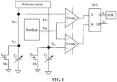
- FIG. 1 is an oscillator circuit diagram.
- Capacitors C 1 and C 2 are charged by the reference currents I ch1 and I ch2 .
- comparators comp 1 and comp 2 flip to set or reset a DFF.
- An output signal S 1 or S 2 flips and discharges the corresponding capacitor, until a clock signal is generated based on cyclic actions.
- Factors such as process deviation and temperature variation may cause the reference current to change, and the change of the reference current may affect charging time of the capacitor, and then affect a frequency of the clock signal, resulting in insufficient accuracy of an oscillator frequency.
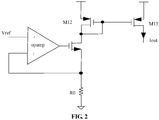
- FIG. 2 illustrates a reference current generating circuit frequently used in a chip.
- the voltage across a resistor R0 is also Vref, such that the current flowing through the resistor is Vref/R0.
- the generated current may be outputted to other modules for use.
- the Vref may be obtained by dividing an internal bandgap voltage, and generally the Vref may be trimmed to obtain a reference voltage Vref having a higher precision.
- the finally obtained Vref is insensitive to variations of processes, voltages, and temperatures.
- a technical problem to be solved by the present disclosure is to provide an on-chip reference current generating circuit, which can supply a stable reference current.
- the present disclosure provides an on-chip reference current generating circuit for supplying at least one reference current to at least one load.
- the on-chip reference current generating circuit includes a transistor, an operational amplifier unit, a first pull-down resistor unit, and a current mirror unit.
- a reference voltage is inputted to a positive input terminal of the operational amplifier unit, a negative input terminal of the operational amplifier unit is coupled to a source of the transistor, and an output terminal of the operational amplifier unit is coupled to a gate of the transistor.
- the first pull-down resistor unit is coupled between the source of the transistor and a ground.
- the current mirror unit is coupled between a drain of the transistor and a power supply voltage and is configured to output a generated current to the load for use.
- first pull-down resistor unit is arranged adjacent to the second pull-down resistor unit.
- the reference voltage is much less than 2(V GS -V TH ).
- the reference voltage is 1/100 ⁇ 1/10 of 2(V GS -V TH ).
- bypass resistor unit includes at least one transistor.
- the source of the at least one transistor in the bypass resistor unit is grounded.
- the first pull-down resistor unit includes a plurality of transistors coupled in parallel.
- the on-chip reference current generating circuit also includes a bandgap voltage generator.
- the bandgap voltage generator is coupled to the positive input terminal of the operational amplifier unit and is configured to generate the reference voltage.
- the transistor is an N-type transistor.
- an advantage of the present disclosure is as below. After the first pull-down resistor unit of the on-chip reference current generating circuit is calibrated by the ZQ calibration circuit, an equivalent resistance of the first pull-down resistor unit is insensitive to variations of processes, voltages, and temperatures, such that the reference current outputted from the current mirror unit may not vary greatly with the processes, the voltages, and the temperatures. Therefore, the on-chip reference current generating circuit provided by the present disclosure can supply a stable reference current.
- the on-chip reference current generating circuit provided by the present disclosure is arranged in a chip 1 to supply at least one reference current to at least one load.
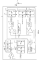
- FIG. 3 is a circuit diagram of a first embodiment of the on-chip reference current generating circuit according to the present disclosure.
- the on-chip reference current generating circuit includes a transistor M1, an operational amplifier unit opamp, a current mirror unit 12, and a first pull-down resistor unit 10.
- the transistor M1 is an N-type transistor.
- a reference voltage Vrefl is inputted to a positive input terminal of the operational amplifier unit opamp, a negative input terminal of the operational amplifier unit opamp is coupled to a source of the transistor M1, and an output terminal of the operational amplifier unit opamp is coupled to a gate of the transistor M1.
- the reference voltage is generated by a bandgap voltage generator 102.
- the bandgap voltage generator 102 is coupled to the positive input terminal of the operational amplifier unit opamp, and is configured to transmit the generated reference voltage to the positive input terminal of the operational amplifier unit opamp.
- the current mirror unit 12 is coupled between a drain of the transistor M1 and a power supply voltage and is configured to output a current generated by the on-chip reference current generating circuit to the load for use.
- the current mirror unit 12 is composed of a P-type transistor M12 and a P-type transistor M13.
- the P-type transistor M12 has a source connected to a power supply potential, and a gate and a drain connected to the drain of the transistor M1.
- the P-type transistor M13 has a source connected to the power supply potential, and a gate connected to a gate and a drain of the P-type transistor M12. A drain of the P-type transistor M13 outputs a reference current.
- circuits in other forms may also be used as the current mirror unit.
- the current mirror unit 12 can implement replication or multiplication of a current signal. Specifically, in this embodiment, the current mirror unit 12 replicates a current flowing through the first pull-down resistor unit 10, and outputs the current as the reference current.
- the first pull-down resistor unit 10 is coupled between the source of the transistor M1 and a ground.
- the on-chip reference current generating circuit ensures that a voltage, whose magnitude is also Vrefl, across the first pull-down resistor unit 10 is equal to the reference voltage Vrefl.
- the current flowing through the first pull-down resistor unit 10 is Vref1/R0.
- the current mirror unit 12 composed of the P-type transistor M12 and the P-type transistor M13 outputs the generated current as the reference current to other modules for use.
- the first pull-down resistor unit 10 is not a polycrystalline resistor, but is a resistor unit calibrated by a ZQ calibration circuit 100.
- the first pull-down resistor unit 10 includes a plurality of transistors coupled in parallel.
- a memory chip such as DDR4 generally has a ZQ calibration function.
- a pull-up unit and a pull-down unit are calibrated by the ZQ calibration circuit, such that equivalent resistance of the pull-up unit and the pull-down unit meet accuracy requirements. That is, the equivalent resistances of the pull-up unit and the pull-down unit calibrated are insensitive to variations of processes, voltages, and temperatures.
- the ZQ calibration circuit 100 includes a first pull-up resistor unit 110, a second pull-up resistor unit 120, a second pull-down resistor unit 130, a reference voltage generator 102, a first comparator 103, a second comparator 104, a P code counter 105, and an N code counter 106.
- the ZQ calibration includes a pull-up calibration and a pull-down calibration.
- a method for the pull-up calibration is as below.
- a power supply voltage VDDQ is divided by the first pull-up resistor unit 110 and a reference resistor 101 to supply a voltage to a node ZQ.
- the reference resistor 101 connected to a pin coupled to the node ZQ generally has a resistance of 240 ⁇ .
- the first comparator 103 compares the voltage at the node ZQ with a reference voltage Vref2 outputted from the bandgap voltage generator 102, to generate an up/down signal UP/DN.
- the reference voltage Vre2f generally is set to be a half of the supplied voltage, i.e., VDDQ/2.
- the P code counter 105 receives the up/down signal UP/DN, to generate a binary code PCODE ⁇ 0:N> as the pull-up calibration code.
- the binary code PCODE ⁇ 0:N> enables/disables MOS transistors coupled in parallel in the first pull-up resistor unit 110 to calibrate the resistance of the first pull-up resistor unit 110.
- the calibrated resistance of the first pull-up resistor unit 110 has an effect on the voltage at the node ZQ. The above operation is repeated. That is, the pull-up calibration is performed on the first pull-up resistor unit 110, such that the resistance of the first pull-up resistor unit 110 becomes equal to the resistance of the reference resistor 101.
- the binary code PCODE ⁇ 0:N> generated during the pull-up calibration is also inputted to the second pull-up resistor unit 120, and the resistance of the second pull-up resistor unit 120 is determined.
- the pull-down calibration is performed.
- a binary code NCODE ⁇ 0:N> generated by the second comparator 104 and the N code counter 106 is used as a pull-down calibration code.
- the pull-down calibration code By using the pull-down calibration code, the voltage at the node NODE becomes equal to the reference voltage Vref2.
- the pull-down calibration is performed, such that the resistance of the second pull-down resistor unit 130 becomes equal to the resistance of the second pull-up resistor unit 120.
- the binary codes PCODE ⁇ 0:N> and NCODE ⁇ 0:N> generated by the ZQ calibration are inputted to an input/output circuit to calibrate each resistor of the resistor units.
- the binary codes PCODE ⁇ 0:N> and NCODE ⁇ 0:N> are connected to the resistances of the pull-up and pull-down resistors of a DQ pad.
- the pull-up and pull-down resistors have layouts similar to those of the above pull-up and pull-down resistor units.
- a ZQ calibration controller 107 and a time counter 108 are employed to control the ZQ calibration.
- the equivalent resistances of the calibrated first pull-up resistor unit 110 and the calibrated second pull-down resistor unit 130 are insensitive to variations of processes, voltages and temperatures.
- the on-chip reference current generating circuit uses the pull-down calibration code NCODE ⁇ 0:N> of the ZQ calibration circuit, and duplicates the second pull-down resistor unit 130 of the ZQ calibration circuit as the first pull-down resistor unit 10 of the on-chip reference current generating circuit provided by the present disclosure.
- the first pull-down resistor unit 10 is determined as a resistor unit calibrated by the ZQ calibration circuit, and the equivalent resistance of the first pull-down resistor unit 10 is insensitive to variations of processes, voltages and temperatures.
- the first pull-down resistor unit 10 and the second pull-down resistor unit 130 are strictly matched in layout, placement and routing.
- MOS transistors corresponding to the first pull-down resistor unit 10 and the second pull-down resistor unit 130 adopt the same size and arrangement direction. Furthermore, the first pull-down resistor unit 10 and the second pull-down resistor unit 130 adopt the same control signal, i.e., the pull-down calibration code NCODE ⁇ 0:N>.
- the first pull-down resistor unit 10 is arranged adjacent to the second pull-down resistor unit 130 to prevent other influence factors from causing different calibrations on the first pull-down resistor unit 10 and the second pull-down resistor unit 130 by the ZQ calibration circuit, thereby reducing the sensitivity of the equivalent resistance of the first pull-down resistor unit 10 to the variations of processes, voltages and temperatures.
- the value of the reference voltage Vrefl of the on-chip reference current generating circuit provided by the present disclosure is not allowed to be too large.
- the value of the reference voltage Vrefl of the on-chip reference current generating circuit provided by the present disclosure is less than 2(V GS -V TH ), such that the MOS transistor in the first pull-down resistor unit 10 is in a triode region, where VGS represents a gate-source voltage of the MOS transistor in the first pull-down resistor unit 10, and V TH represents a breakdown voltage of the MOS transistor in the first pull-down resistor unit 10.
- the value of the reference voltage Vrefl is much smaller than 2(V GS -V TH ).
- the value of the reference voltage Vrefl is 1/100 ⁇ 1/10 of 2(V GS -V TH ), such that the MOS transistor in the first pull-down resistor unit 10 is in a deep triode region, and the first pull-down resistor unit 10 is closer to the real resistance.
- the on-chip reference current generating circuit In the on-chip reference current generating circuit provided by the present disclosure, a traditional on-chip resistor is replaced with the first pull-down resistor unit 10 calibrated by the ZQ calibration circuit.
- the equivalent resistance of the first pull-down resistor unit 10 calibrated by the ZQ calibration circuit may not vary greatly with temperature or process tolerances, and the reference current outputted from the current mirror unit 12 may not vary greatly with the temperature or process tolerances. Therefore, the on-chip reference current generating circuit provided by the present disclosure can supply a stable reference current.
- FIG. 4 is a circuit diagram of the on-chip reference current generating circuit according to the second embodiment of the present disclosure.
- the on-chip reference current generating circuit further includes a bypass resistor unit 13 connected in parallel with the first pull-down resistor unit 10.
- the bypass resistor unit 13 is enabled before the first pull-down resistor unit 10 is calibrated by the ZQ calibration circuit 100, to ensure that there is still a current path.
- the bypass resistor unit 13 is disabled after the first pull-down resistor unit 10 is calibrated by the ZQ calibration circuit 100, which has no influence on the normal operation of the reference current generating circuit.
- the bypass resistor unit 13 includes at least one transistor.
- the transistor is an NMOS transistor.
- the source of the transistor is grounded, and a control signal Ctrl is inputted to the gate of the transistor.
- the control signal Ctrl is high, the transistor is enabled, and the bypass resistor unit 13 is grounded, to ensure that there is still a current path in the on-chip reference current generating circuit.
- the bypass resistor unit 13 is disabled after the ZQ calibration function works, which has no influence on the normal operation of the reference current generating circuit.
- the control signal Ctrl may be generated by a controller of an integrated circuit.
Landscapes
- Engineering & Computer Science (AREA)
- Physics & Mathematics (AREA)
- Microelectronics & Electronic Packaging (AREA)
- General Physics & Mathematics (AREA)
- Electromagnetism (AREA)
- Computer Hardware Design (AREA)
- Radar, Positioning & Navigation (AREA)
- Automation & Control Theory (AREA)
- General Engineering & Computer Science (AREA)
- Mathematical Physics (AREA)
- Computing Systems (AREA)
- Nonlinear Science (AREA)
- Semiconductor Integrated Circuits (AREA)
- Control Of Electrical Variables (AREA)
Abstract
Description
- This application claims priority to
Chinese Patent Application No. 201910981700.6 - The present disclosure relates to the field of integrated circuit, and more particularly, to an on-chip reference current generating circuit.
- A reference current is a current insensitive to variations of factors such as temperatures, voltages, and processes. The reference current is widely used in design of integrated circuits. For example, an oscillator circuit formed by charging and discharging a capacitor with the reference current may be used in a charge pump circuit in a DRAM.
FIG. 1 is an oscillator circuit diagram. Capacitors C1 and C2 are charged by the reference currents Ich1 and Ich2. When voltages across the capacitors C1 and C2 are charged to be the same as the reference voltage Vbg, comparators comp1 and comp2 flip to set or reset a DFF. An output signal S1 or S2 flips and discharges the corresponding capacitor, until a clock signal is generated based on cyclic actions. Factors such as process deviation and temperature variation may cause the reference current to change, and the change of the reference current may affect charging time of the capacitor, and then affect a frequency of the clock signal, resulting in insufficient accuracy of an oscillator frequency. -
FIG. 2 illustrates a reference current generating circuit frequently used in a chip. With reference toFIG. 2 , by means of a clamping action of an operational amplifier amp, the voltage across a resistor R0 is also Vref, such that the current flowing through the resistor is Vref/R0. Through a current mirror composed of a transistor M12 and a transistor M13, the generated current may be outputted to other modules for use. The Vref may be obtained by dividing an internal bandgap voltage, and generally the Vref may be trimmed to obtain a reference voltage Vref having a higher precision. The finally obtained Vref is insensitive to variations of processes, voltages, and temperatures. As an on-chip resistor, R0 generally is a polycrystalline resistor, and its resistance may vary greatly with temperature or process tolerances, which causes a consequence that the finally outputted current (i.e., the reference current) may also vary greatly with temperature or process tolerances. If the R0 is an off-chip resistor, it may occupy additional pin resources, which is disadvantageous to the miniaturization of components, and may inevitably consume a lot of space and increase production costs, and thus is not economical. - Therefore, how to enable an on-chip reference current generating circuit to output a stable reference current becomes a technology that needs to be solved urgently.
- A technical problem to be solved by the present disclosure is to provide an on-chip reference current generating circuit, which can supply a stable reference current.
- To solve the above problem, the present disclosure provides an on-chip reference current generating circuit for supplying at least one reference current to at least one load. The on-chip reference current generating circuit includes a transistor, an operational amplifier unit, a first pull-down resistor unit, and a current mirror unit. A reference voltage is inputted to a positive input terminal of the operational amplifier unit, a negative input terminal of the operational amplifier unit is coupled to a source of the transistor, and an output terminal of the operational amplifier unit is coupled to a gate of the transistor. As a resistor unit calibrated by a ZQ calibration circuit, the first pull-down resistor unit is coupled between the source of the transistor and a ground. The current mirror unit is coupled between a drain of the transistor and a power supply voltage and is configured to output a generated current to the load for use.
- Further, the ZQ calibration circuit has a second pull-down resistor unit and a pull-down calibration code for calibrating the second pull-down resistor unit. The first pull-down resistor unit duplicates the second pull-down resistor unit, and uses the pull-down calibration code as a pull-down calibration code of the first pull-down resistor unit.
- Further, the first pull-down resistor unit is arranged adjacent to the second pull-down resistor unit.
- Further, the reference voltage is much less than 2(VGS-VTH).
- Further, the reference voltage is 1/100~1/10 of 2(VGS-VTH).
- Further, the on-chip reference current generating circuit also includes a bypass resistor unit connected in parallel with the first pull-down resistor unit. The bypass resistor unit is enabled before the first pull-down resistor unit is calibrated by the ZQ calibration circuit, and the bypass resistor unit is disabled after the first pull-down resistor unit is calibrated by the ZQ calibration circuit.
- Further, the bypass resistor unit includes at least one transistor.
- Further, the source of the at least one transistor in the bypass resistor unit is grounded.
- Further, the first pull-down resistor unit includes a plurality of transistors coupled in parallel.
- Further, the on-chip reference current generating circuit also includes a bandgap voltage generator. The bandgap voltage generator is coupled to the positive input terminal of the operational amplifier unit and is configured to generate the reference voltage.
- Further, the transistor is an N-type transistor.
- An advantage of the present disclosure is as below. After the first pull-down resistor unit of the on-chip reference current generating circuit is calibrated by the ZQ calibration circuit, an equivalent resistance of the first pull-down resistor unit is insensitive to variations of processes, voltages, and temperatures, such that the reference current outputted from the current mirror unit may not vary greatly with the processes, the voltages, and the temperatures. Therefore, the on-chip reference current generating circuit provided by the present disclosure can supply a stable reference current.
-
-
FIG. 1 is a circuit diagram of an existing oscillator; -
FIG. 2 is a reference current generating circuit frequently used in an existing chip; -
FIG. 3 is a circuit diagram of a first embodiment of an on-chip reference current generating circuit according to the present disclosure; and -
FIG. 4 is a circuit diagram of a second embodiment of an on-chip reference current generating circuit according to the present disclosure. - Embodiments of the on-chip reference current generating circuit provided by the present disclosure are described below in detail with reference to the accompanying drawings.
- The on-chip reference current generating circuit provided by the present disclosure is arranged in a
chip 1 to supply at least one reference current to at least one load.FIG. 3 is a circuit diagram of a first embodiment of the on-chip reference current generating circuit according to the present disclosure. With reference toFIG. 3 , the on-chip reference current generating circuit includes a transistor M1, an operational amplifier unit opamp, acurrent mirror unit 12, and a first pull-down resistor unit 10. In this embodiment, the transistor M1 is an N-type transistor. - A reference voltage Vrefl is inputted to a positive input terminal of the operational amplifier unit opamp, a negative input terminal of the operational amplifier unit opamp is coupled to a source of the transistor M1, and an output terminal of the operational amplifier unit opamp is coupled to a gate of the transistor M1. In the embodiment, the reference voltage is generated by a
bandgap voltage generator 102. Thebandgap voltage generator 102 is coupled to the positive input terminal of the operational amplifier unit opamp, and is configured to transmit the generated reference voltage to the positive input terminal of the operational amplifier unit opamp. - The
current mirror unit 12 is coupled between a drain of the transistor M1 and a power supply voltage and is configured to output a current generated by the on-chip reference current generating circuit to the load for use. In this embodiment, thecurrent mirror unit 12 is composed of a P-type transistor M12 and a P-type transistor M13. The P-type transistor M12 has a source connected to a power supply potential, and a gate and a drain connected to the drain of the transistor M1. The P-type transistor M13 has a source connected to the power supply potential, and a gate connected to a gate and a drain of the P-type transistor M12. A drain of the P-type transistor M13 outputs a reference current. In other embodiments of the present disclosure, circuits in other forms may also be used as the current mirror unit. Thecurrent mirror unit 12 can implement replication or multiplication of a current signal. Specifically, in this embodiment, thecurrent mirror unit 12 replicates a current flowing through the first pull-downresistor unit 10, and outputs the current as the reference current. - With an equivalent resistance of R0, the first pull-
down resistor unit 10 is coupled between the source of the transistor M1 and a ground. By means of a clamping action of the operational amplifier unit 11, the on-chip reference current generating circuit ensures that a voltage, whose magnitude is also Vrefl, across the first pull-down resistor unit 10 is equal to the reference voltage Vrefl. In this case, the current flowing through the first pull-down resistor unit 10 is Vref1/R0. Thecurrent mirror unit 12 composed of the P-type transistor M12 and the P-type transistor M13 outputs the generated current as the reference current to other modules for use. - As described in the background art, if the first pull-
down resistor unit 10 is a resistor, its resistance may vary greatly with temperature or process tolerances, which causes a consequence that the finally outputted reference current may also vary greatly with temperature or process tolerances. Therefore, in order to overcome the above technical problem, in an embodiment of the present disclosure, the first pull-down resistor unit 10 is not a polycrystalline resistor, but is a resistor unit calibrated by aZQ calibration circuit 100. For example, the first pull-down resistor unit 10 includes a plurality of transistors coupled in parallel. - A memory chip such as DDR4 generally has a ZQ calibration function. A pull-up unit and a pull-down unit are calibrated by the ZQ calibration circuit, such that equivalent resistance of the pull-up unit and the pull-down unit meet accuracy requirements. That is, the equivalent resistances of the pull-up unit and the pull-down unit calibrated are insensitive to variations of processes, voltages, and temperatures.
- Specifically, with reference to
FIG. 3 , theZQ calibration circuit 100 includes a first pull-upresistor unit 110, a second pull-upresistor unit 120, a second pull-down resistor unit 130, areference voltage generator 102, afirst comparator 103, asecond comparator 104, aP code counter 105, and anN code counter 106. The ZQ calibration includes a pull-up calibration and a pull-down calibration. - A method for the pull-up calibration is as below. A power supply voltage VDDQ is divided by the first pull-up
resistor unit 110 and areference resistor 101 to supply a voltage to a node ZQ. Thereference resistor 101 connected to a pin coupled to the node ZQ generally has a resistance of 240Ω. Thefirst comparator 103 compares the voltage at the node ZQ with a reference voltage Vref2 outputted from thebandgap voltage generator 102, to generate an up/down signal UP/DN. The reference voltage Vre2f generally is set to be a half of the supplied voltage, i.e., VDDQ/2. TheP code counter 105 receives the up/down signal UP/DN, to generate a binary code PCODE<0:N> as the pull-up calibration code. The binary code PCODE<0:N> enables/disables MOS transistors coupled in parallel in the first pull-upresistor unit 110 to calibrate the resistance of the first pull-upresistor unit 110. The calibrated resistance of the first pull-upresistor unit 110 has an effect on the voltage at the node ZQ. The above operation is repeated. That is, the pull-up calibration is performed on the first pull-upresistor unit 110, such that the resistance of the first pull-upresistor unit 110 becomes equal to the resistance of thereference resistor 101. The binary code PCODE<0:N> generated during the pull-up calibration is also inputted to the second pull-upresistor unit 120, and the resistance of the second pull-upresistor unit 120 is determined. - Similar to performing the pull-up calibration, the pull-down calibration is performed. A binary code NCODE<0:N> generated by the
second comparator 104 and theN code counter 106 is used as a pull-down calibration code. By using the pull-down calibration code, the voltage at the node NODE becomes equal to the reference voltage Vref2. The pull-down calibration is performed, such that the resistance of the second pull-down resistor unit 130 becomes equal to the resistance of the second pull-upresistor unit 120. - The binary codes PCODE<0:N> and NCODE<0:N> generated by the ZQ calibration are inputted to an input/output circuit to calibrate each resistor of the resistor units. In the case of a semiconductor memory device, it is determined that the binary codes PCODE<0:N> and NCODE<0:N> are connected to the resistances of the pull-up and pull-down resistors of a DQ pad. The pull-up and pull-down resistors have layouts similar to those of the above pull-up and pull-down resistor units. Further, a
ZQ calibration controller 107 and atime counter 108 are employed to control the ZQ calibration. - After the first pull-up
resistor unit 110 and the second pull-down resistor unit 130 are calibrated by theZQ calibration circuit 100, their equivalent resistances meet the accuracy requirements. That is, the equivalent resistances of the calibrated first pull-upresistor unit 110 and the calibrated second pull-down resistor unit 130 are insensitive to variations of processes, voltages and temperatures. - In view of the above advantages of the ZQ calibration circuit, the on-chip reference current generating circuit provided by the present disclosure uses the pull-down calibration code NCODE<0:N> of the ZQ calibration circuit, and duplicates the second pull-
down resistor unit 130 of the ZQ calibration circuit as the first pull-down resistor unit 10 of the on-chip reference current generating circuit provided by the present disclosure. In this case, the first pull-down resistor unit 10 is determined as a resistor unit calibrated by the ZQ calibration circuit, and the equivalent resistance of the first pull-down resistor unit 10 is insensitive to variations of processes, voltages and temperatures. In this embodiment, the first pull-down resistor unit 10 and the second pull-down resistor unit 130 are strictly matched in layout, placement and routing. MOS transistors corresponding to the first pull-down resistor unit 10 and the second pull-down resistor unit 130 adopt the same size and arrangement direction. Furthermore, the first pull-down resistor unit 10 and the second pull-down resistor unit 130 adopt the same control signal, i.e., the pull-down calibration code NCODE<0:N>. - Preferably, in the layout and placement, the first pull-
down resistor unit 10 is arranged adjacent to the second pull-down resistor unit 130 to prevent other influence factors from causing different calibrations on the first pull-down resistor unit 10 and the second pull-down resistor unit 130 by the ZQ calibration circuit, thereby reducing the sensitivity of the equivalent resistance of the first pull-down resistor unit 10 to the variations of processes, voltages and temperatures. - Further, to ensure the first pull-
down resistor unit 10 to be closer to a real resistance, the value of the reference voltage Vrefl of the on-chip reference current generating circuit provided by the present disclosure is not allowed to be too large. Preferably, the value of the reference voltage Vrefl of the on-chip reference current generating circuit provided by the present disclosure is less than 2(VGS-VTH), such that the MOS transistor in the first pull-down resistor unit 10 is in a triode region, where VGS represents a gate-source voltage of the MOS transistor in the first pull-down resistor unit 10, and VTH represents a breakdown voltage of the MOS transistor in the first pull-down resistor unit 10. Preferably, the value of the reference voltage Vrefl is much smaller than 2(VGS-VTH). For example, the value of the reference voltage Vrefl is 1/100∼1/10 of 2(VGS-VTH), such that the MOS transistor in the first pull-down resistor unit 10 is in a deep triode region, and the first pull-down resistor unit 10 is closer to the real resistance. - In the on-chip reference current generating circuit provided by the present disclosure, a traditional on-chip resistor is replaced with the first pull-
down resistor unit 10 calibrated by the ZQ calibration circuit. The equivalent resistance of the first pull-down resistor unit 10 calibrated by the ZQ calibration circuit may not vary greatly with temperature or process tolerances, and the reference current outputted from thecurrent mirror unit 12 may not vary greatly with the temperature or process tolerances. Therefore, the on-chip reference current generating circuit provided by the present disclosure can supply a stable reference current. - In addition, it is found that when the ZQ calibration circuit is initialized, the first pull-
down resistor unit 10 is completely disabled, and thus no current can be generated, which may have an influence on the generation of the reference current. To prevent the occurrence of the above problem, the present disclosure also provides a second embodiment of the on-chip reference current generating circuit.FIG. 4 is a circuit diagram of the on-chip reference current generating circuit according to the second embodiment of the present disclosure. With reference toFIG. 4 , to prevent the influence on the generation of the reference current caused by failed generation of the current due to that the first pull-down resistor unit 10 is completely disabled when the ZQ calibration circuit is initialized, the on-chip reference current generating circuit further includes abypass resistor unit 13 connected in parallel with the first pull-down resistor unit 10. Thebypass resistor unit 13 is enabled before the first pull-down resistor unit 10 is calibrated by theZQ calibration circuit 100, to ensure that there is still a current path. Thebypass resistor unit 13 is disabled after the first pull-down resistor unit 10 is calibrated by theZQ calibration circuit 100, which has no influence on the normal operation of the reference current generating circuit. - In this embodiment, the
bypass resistor unit 13 includes at least one transistor. In this embodiment, the transistor is an NMOS transistor. The source of the transistor is grounded, and a control signal Ctrl is inputted to the gate of the transistor. When the transistor of the first pull-down resistor unit 10 is not enabled, the control signal Ctrl is high, the transistor is enabled, and thebypass resistor unit 13 is grounded, to ensure that there is still a current path in the on-chip reference current generating circuit. Thebypass resistor unit 13 is disabled after the ZQ calibration function works, which has no influence on the normal operation of the reference current generating circuit. The control signal Ctrl may be generated by a controller of an integrated circuit. - The above descriptions are merely the preferred embodiments of the present invention. It should be noted that those of ordinary skill in the art may make several improvements and modifications without departing from the principle of the present invention, and these improvements and modifications should also be considered as in the protection scope of the present invention.
Claims (11)
- An on-chip reference current generating circuit for supplying at least one reference current to at least one load, the on-chip reference current generating circuit comprising:a transistor;an operational amplifier unit, a reference voltage being inputted to a positive input terminal of the operational amplifier unit, a negative input terminal of the operational amplifier unit being coupled to a source of the transistor, and an output terminal of the operational amplifier unit being coupled to a gate of the transistor;a first pull-down resistor unit coupled between the source of the transistor and a ground, the first pull-down resistor unit being a resistor unit calibrated by a ZQ calibration circuit; anda current mirror unit coupled between a drain of the transistor and a power supply voltage, wherein the current mirror unit is configured to output a generated current to the load for use.
- The on-chip reference current generating circuit of claim 1, wherein the ZQ calibration circuit has a second pull-down resistor unit and a pull-down calibration code configured for calibrating the second pull-down resistor unit, wherein
the first pull-down resistor unit is configured to duplicate the second pull-down resistor unit, and use the pull-down calibration code as a pull-down calibration code of the first pull-down resistor unit. - The on-chip reference current generating circuit of claim 2, wherein the first pull-down resistor unit is arranged adjacent to the second pull-down resistor unit.
- The on-chip reference current generating circuit of claim 1, wherein the reference voltage is less than 2(VGS-VTH).
- The on-chip reference current generating circuit of claim 4, wherein the reference voltage is 1/100∼1/10 of 2(VGS-VTH).
- The on-chip reference current generating circuit of claim 1, further comprising a bypass resistor unit connected in parallel with the first pull-down resistor unit, wherein the bypass resistor unit is enabled before the first pull-down resistor unit is calibrated by the ZQ calibration circuit, and the bypass resistor unit is disabled after the first pull-down resistor unit is calibrated by the ZQ calibration circuit.
- The on-chip reference current generating circuit of claim 6, wherein the bypass resistor unit comprises at least one transistor.
- The on-chip reference current generating circuit of claim 7, wherein the source of the at least one transistor in the bypass resistor unit is grounded.
- The on-chip reference current generating circuit of claim 1, wherein the first pull-down resistor unit comprises a plurality of transistors coupled in parallel.
- The on-chip reference current generating circuit of claim 1, further comprising a bandgap voltage generator, wherein the bandgap voltage generator is coupled to a positive input terminal of the operational amplifier unit and is configured to generate the reference voltage.
- The on-chip reference current generating circuit of claim 1, wherein the transistor is an N-type transistor.
Applications Claiming Priority (2)
| Application Number | Priority Date | Filing Date | Title |
|---|---|---|---|
| CN201910981700.6A CN112667022A (en) | 2019-10-16 | 2019-10-16 | On-chip reference current generation circuit |
| PCT/CN2020/095337 WO2021073126A1 (en) | 2019-10-16 | 2020-06-10 | In-chip reference current generation circuit |
Publications (3)
| Publication Number | Publication Date |
|---|---|
| EP3893079A1 true EP3893079A1 (en) | 2021-10-13 |
| EP3893079A4 EP3893079A4 (en) | 2022-04-20 |
| EP3893079B1 EP3893079B1 (en) | 2023-12-27 |
Family
ID=75400213
Family Applications (1)
| Application Number | Title | Priority Date | Filing Date |
|---|---|---|---|
| EP20877533.8A Active EP3893079B1 (en) | 2019-10-16 | 2020-06-10 | In-chip reference current generation circuit |
Country Status (4)
| Country | Link |
|---|---|
| US (1) | US20210208618A1 (en) |
| EP (1) | EP3893079B1 (en) |
| CN (1) | CN112667022A (en) |
| WO (1) | WO2021073126A1 (en) |
Families Citing this family (5)
| Publication number | Priority date | Publication date | Assignee | Title |
|---|---|---|---|---|
| US11442485B2 (en) * | 2020-07-09 | 2022-09-13 | Novatek Microelectronics Corp. | Integrated circuit chip and test method thereof |
| CN117316256A (en) * | 2022-06-22 | 2023-12-29 | 长鑫存储技术有限公司 | Single-loop and dual-loop memory devices and ZQ calibration methods |
| CN115265861B (en) * | 2022-07-27 | 2025-07-18 | 深圳数马电子技术有限公司 | Pressure sensing circuit with temperature compensation and pressure detection equipment |
| CN120994008A (en) * | 2025-02-11 | 2025-11-21 | 上海安其威微电子科技有限公司 | Current compensation circuit, logarithmic detector and chip |
| CN119851625B (en) * | 2025-02-18 | 2026-05-12 | 南宁初芯集成电路设计有限公司 | Positive and negative pressure source driving circuit |
Family Cites Families (8)
| Publication number | Priority date | Publication date | Assignee | Title |
|---|---|---|---|---|
| US7692446B2 (en) * | 2006-08-24 | 2010-04-06 | Hynix Semiconductor, Inc. | On-die termination device |
| CN101676828B (en) * | 2008-09-19 | 2012-01-11 | 智原科技股份有限公司 | Reference current generation circuit for low operating voltage |
| US20100259315A1 (en) * | 2009-04-08 | 2010-10-14 | Taiwan Semiconductor Manufacturing Company, Ltd. | Circuit and Methods for Temperature Insensitive Current Reference |
| CN102419609B (en) * | 2010-09-27 | 2015-07-08 | 联咏科技股份有限公司 | Reference voltage and reference current generating circuit |
| US20160231766A1 (en) * | 2013-01-28 | 2016-08-11 | Xinfeng Quantel Technologies (Beijing) Co., Ltd. | Self-calibration current source system |
| US9704591B2 (en) * | 2014-12-17 | 2017-07-11 | Sandisk Technologies Llc | Temperature independent reference current generation for calibration |
| CN107239092B (en) * | 2016-03-28 | 2019-08-06 | 桑迪士克科技有限责任公司 | Temperature-Independent Reference Current Generation for Calibration |
| US10429874B1 (en) * | 2018-12-20 | 2019-10-01 | Nxp B.V. | Reference voltage circuit with current buffer |
-
2019
- 2019-10-16 CN CN201910981700.6A patent/CN112667022A/en active Pending
-
2020
- 2020-06-10 WO PCT/CN2020/095337 patent/WO2021073126A1/en not_active Ceased
- 2020-06-10 EP EP20877533.8A patent/EP3893079B1/en active Active
-
2021
- 2021-03-03 US US17/190,405 patent/US20210208618A1/en not_active Abandoned
Also Published As
| Publication number | Publication date |
|---|---|
| CN112667022A (en) | 2021-04-16 |
| EP3893079A4 (en) | 2022-04-20 |
| WO2021073126A1 (en) | 2021-04-22 |
| US20210208618A1 (en) | 2021-07-08 |
| EP3893079B1 (en) | 2023-12-27 |
Similar Documents
| Publication | Publication Date | Title |
|---|---|---|
| EP3893079B1 (en) | In-chip reference current generation circuit | |
| US9899989B2 (en) | Calibration circuit, integrated circuit having calibration circuit, and calibration method | |
| JP4648346B2 (en) | Adjustable transistor body bias network | |
| US8593887B2 (en) | Semiconductor device having reference voltage generating unit | |
| US9136827B2 (en) | Power-on reset circuit | |
| US8786324B1 (en) | Mixed voltage driving circuit | |
| CN110198154B (en) | Variable resistor circuit, oscillating circuit and semiconductor device | |
| US7646222B2 (en) | Semiconductor device for generating power on reset signal | |
| US20080157832A1 (en) | Power-On-Reset Circuit | |
| US6813194B2 (en) | Bias distribution network for digital multilevel nonvolatile flash memory | |
| US20200292587A1 (en) | Current sensing circuit | |
| US8618786B1 (en) | Self-biased voltage regulation circuitry for memory | |
| US20190086355A1 (en) | Semiconductor apparatus including a capacitance measuring circuit | |
| US9503019B2 (en) | Apparatuses and methods for providing oscillation signals | |
| US11313906B2 (en) | Auto-calibration circuit for pulse generating circuit used in resonating circuits | |
| KR100607164B1 (en) | Reference voltage generator | |
| US6522591B2 (en) | Semiconductor memory circuit | |
| US11688434B2 (en) | Internal voltage generation circuit and semiconductor memory apparatus including the same | |
| US9437258B2 (en) | Data readout circuit of a storage device for read-out operation for preventing erroneous writing into a data storage element and reading out of the data correctly | |
| CN116482564A (en) | Power detection device and power detection method | |
| US11249504B2 (en) | Current generation circuit | |
| US6788100B2 (en) | Resistor mirror | |
| KR100940825B1 (en) | Power-Up Circuits in Semiconductor Integrated Circuits | |
| CN119853656A (en) | Power-on reset circuit, chip and electronic equipment | |
| KR102614973B1 (en) | Process information extractor circuit |
Legal Events
| Date | Code | Title | Description |
|---|---|---|---|
| STAA | Information on the status of an ep patent application or granted ep patent |
Free format text: STATUS: THE INTERNATIONAL PUBLICATION HAS BEEN MADE |
|
| PUAI | Public reference made under article 153(3) epc to a published international application that has entered the european phase |
Free format text: ORIGINAL CODE: 0009012 |
|
| STAA | Information on the status of an ep patent application or granted ep patent |
Free format text: STATUS: REQUEST FOR EXAMINATION WAS MADE |
|
| 17P | Request for examination filed |
Effective date: 20210709 |
|
| AK | Designated contracting states |
Kind code of ref document: A1 Designated state(s): AL AT BE BG CH CY CZ DE DK EE ES FI FR GB GR HR HU IE IS IT LI LT LU LV MC MK MT NL NO PL PT RO RS SE SI SK SM TR |
|
| A4 | Supplementary search report drawn up and despatched |
Effective date: 20220322 |
|
| RIC1 | Information provided on ipc code assigned before grant |
Ipc: G05F 1/56 20060101ALI20220316BHEP Ipc: G05F 3/26 20060101AFI20220316BHEP |
|
| RIC1 | Information provided on ipc code assigned before grant |
Ipc: G05F 1/56 20060101ALI20221214BHEP Ipc: G05F 3/26 20060101AFI20221214BHEP |
|
| DAV | Request for validation of the european patent (deleted) | ||
| DAX | Request for extension of the european patent (deleted) | ||
| GRAP | Despatch of communication of intention to grant a patent |
Free format text: ORIGINAL CODE: EPIDOSNIGR1 |
|
| STAA | Information on the status of an ep patent application or granted ep patent |
Free format text: STATUS: GRANT OF PATENT IS INTENDED |
|
| INTG | Intention to grant announced |
Effective date: 20230209 |
|
| GRAJ | Information related to disapproval of communication of intention to grant by the applicant or resumption of examination proceedings by the epo deleted |
Free format text: ORIGINAL CODE: EPIDOSDIGR1 |
|
| STAA | Information on the status of an ep patent application or granted ep patent |
Free format text: STATUS: REQUEST FOR EXAMINATION WAS MADE |
|
| INTC | Intention to grant announced (deleted) | ||
| GRAP | Despatch of communication of intention to grant a patent |
Free format text: ORIGINAL CODE: EPIDOSNIGR1 |
|
| STAA | Information on the status of an ep patent application or granted ep patent |
Free format text: STATUS: GRANT OF PATENT IS INTENDED |
|
| P01 | Opt-out of the competence of the unified patent court (upc) registered |
Effective date: 20230530 |
|
| INTG | Intention to grant announced |
Effective date: 20230712 |
|
| GRAS | Grant fee paid |
Free format text: ORIGINAL CODE: EPIDOSNIGR3 |
|
| GRAA | (expected) grant |
Free format text: ORIGINAL CODE: 0009210 |
|
| STAA | Information on the status of an ep patent application or granted ep patent |
Free format text: STATUS: THE PATENT HAS BEEN GRANTED |
|
| AK | Designated contracting states |
Kind code of ref document: B1 Designated state(s): AL AT BE BG CH CY CZ DE DK EE ES FI FR GB GR HR HU IE IS IT LI LT LU LV MC MK MT NL NO PL PT RO RS SE SI SK SM TR |
|
| REG | Reference to a national code |
Ref country code: GB Ref legal event code: FG4D |
|
| REG | Reference to a national code |
Ref country code: CH Ref legal event code: EP |
|
| REG | Reference to a national code |
Ref country code: DE Ref legal event code: R096 Ref document number: 602020023597 Country of ref document: DE |
|
| REG | Reference to a national code |
Ref country code: IE Ref legal event code: FG4D |
|
| PG25 | Lapsed in a contracting state [announced via postgrant information from national office to epo] |
Ref country code: GR Free format text: LAPSE BECAUSE OF FAILURE TO SUBMIT A TRANSLATION OF THE DESCRIPTION OR TO PAY THE FEE WITHIN THE PRESCRIBED TIME-LIMIT Effective date: 20240328 |
|
| REG | Reference to a national code |
Ref country code: LT Ref legal event code: MG9D |
|
| PG25 | Lapsed in a contracting state [announced via postgrant information from national office to epo] |
Ref country code: LT Free format text: LAPSE BECAUSE OF FAILURE TO SUBMIT A TRANSLATION OF THE DESCRIPTION OR TO PAY THE FEE WITHIN THE PRESCRIBED TIME-LIMIT Effective date: 20231227 |
|
| PG25 | Lapsed in a contracting state [announced via postgrant information from national office to epo] |
Ref country code: ES Free format text: LAPSE BECAUSE OF FAILURE TO SUBMIT A TRANSLATION OF THE DESCRIPTION OR TO PAY THE FEE WITHIN THE PRESCRIBED TIME-LIMIT Effective date: 20231227 |
|
| PG25 | Lapsed in a contracting state [announced via postgrant information from national office to epo] |
Ref country code: LT Free format text: LAPSE BECAUSE OF FAILURE TO SUBMIT A TRANSLATION OF THE DESCRIPTION OR TO PAY THE FEE WITHIN THE PRESCRIBED TIME-LIMIT Effective date: 20231227 Ref country code: GR Free format text: LAPSE BECAUSE OF FAILURE TO SUBMIT A TRANSLATION OF THE DESCRIPTION OR TO PAY THE FEE WITHIN THE PRESCRIBED TIME-LIMIT Effective date: 20240328 Ref country code: FI Free format text: LAPSE BECAUSE OF FAILURE TO SUBMIT A TRANSLATION OF THE DESCRIPTION OR TO PAY THE FEE WITHIN THE PRESCRIBED TIME-LIMIT Effective date: 20231227 Ref country code: ES Free format text: LAPSE BECAUSE OF FAILURE TO SUBMIT A TRANSLATION OF THE DESCRIPTION OR TO PAY THE FEE WITHIN THE PRESCRIBED TIME-LIMIT Effective date: 20231227 Ref country code: BG Free format text: LAPSE BECAUSE OF FAILURE TO SUBMIT A TRANSLATION OF THE DESCRIPTION OR TO PAY THE FEE WITHIN THE PRESCRIBED TIME-LIMIT Effective date: 20240327 |
|
| REG | Reference to a national code |
Ref country code: NL Ref legal event code: MP Effective date: 20231227 |
|
| REG | Reference to a national code |
Ref country code: AT Ref legal event code: MK05 Ref document number: 1645130 Country of ref document: AT Kind code of ref document: T Effective date: 20231227 |
|
| PG25 | Lapsed in a contracting state [announced via postgrant information from national office to epo] |
Ref country code: NL Free format text: LAPSE BECAUSE OF FAILURE TO SUBMIT A TRANSLATION OF THE DESCRIPTION OR TO PAY THE FEE WITHIN THE PRESCRIBED TIME-LIMIT Effective date: 20231227 |
|
| PG25 | Lapsed in a contracting state [announced via postgrant information from national office to epo] |
Ref country code: SE Free format text: LAPSE BECAUSE OF FAILURE TO SUBMIT A TRANSLATION OF THE DESCRIPTION OR TO PAY THE FEE WITHIN THE PRESCRIBED TIME-LIMIT Effective date: 20231227 Ref country code: RS Free format text: LAPSE BECAUSE OF FAILURE TO SUBMIT A TRANSLATION OF THE DESCRIPTION OR TO PAY THE FEE WITHIN THE PRESCRIBED TIME-LIMIT Effective date: 20231227 Ref country code: NO Free format text: LAPSE BECAUSE OF FAILURE TO SUBMIT A TRANSLATION OF THE DESCRIPTION OR TO PAY THE FEE WITHIN THE PRESCRIBED TIME-LIMIT Effective date: 20240327 Ref country code: NL Free format text: LAPSE BECAUSE OF FAILURE TO SUBMIT A TRANSLATION OF THE DESCRIPTION OR TO PAY THE FEE WITHIN THE PRESCRIBED TIME-LIMIT Effective date: 20231227 Ref country code: LV Free format text: LAPSE BECAUSE OF FAILURE TO SUBMIT A TRANSLATION OF THE DESCRIPTION OR TO PAY THE FEE WITHIN THE PRESCRIBED TIME-LIMIT Effective date: 20231227 Ref country code: HR Free format text: LAPSE BECAUSE OF FAILURE TO SUBMIT A TRANSLATION OF THE DESCRIPTION OR TO PAY THE FEE WITHIN THE PRESCRIBED TIME-LIMIT Effective date: 20231227 |
|
| PG25 | Lapsed in a contracting state [announced via postgrant information from national office to epo] |
Ref country code: IS Free format text: LAPSE BECAUSE OF FAILURE TO SUBMIT A TRANSLATION OF THE DESCRIPTION OR TO PAY THE FEE WITHIN THE PRESCRIBED TIME-LIMIT Effective date: 20240427 |
|
| PG25 | Lapsed in a contracting state [announced via postgrant information from national office to epo] |
Ref country code: CZ Free format text: LAPSE BECAUSE OF FAILURE TO SUBMIT A TRANSLATION OF THE DESCRIPTION OR TO PAY THE FEE WITHIN THE PRESCRIBED TIME-LIMIT Effective date: 20231227 Ref country code: AT Free format text: LAPSE BECAUSE OF FAILURE TO SUBMIT A TRANSLATION OF THE DESCRIPTION OR TO PAY THE FEE WITHIN THE PRESCRIBED TIME-LIMIT Effective date: 20231227 |
|
| PG25 | Lapsed in a contracting state [announced via postgrant information from national office to epo] |
Ref country code: SK Free format text: LAPSE BECAUSE OF FAILURE TO SUBMIT A TRANSLATION OF THE DESCRIPTION OR TO PAY THE FEE WITHIN THE PRESCRIBED TIME-LIMIT Effective date: 20231227 |
|
| PG25 | Lapsed in a contracting state [announced via postgrant information from national office to epo] |
Ref country code: SM Free format text: LAPSE BECAUSE OF FAILURE TO SUBMIT A TRANSLATION OF THE DESCRIPTION OR TO PAY THE FEE WITHIN THE PRESCRIBED TIME-LIMIT Effective date: 20231227 Ref country code: SK Free format text: LAPSE BECAUSE OF FAILURE TO SUBMIT A TRANSLATION OF THE DESCRIPTION OR TO PAY THE FEE WITHIN THE PRESCRIBED TIME-LIMIT Effective date: 20231227 Ref country code: RO Free format text: LAPSE BECAUSE OF FAILURE TO SUBMIT A TRANSLATION OF THE DESCRIPTION OR TO PAY THE FEE WITHIN THE PRESCRIBED TIME-LIMIT Effective date: 20231227 Ref country code: IT Free format text: LAPSE BECAUSE OF FAILURE TO SUBMIT A TRANSLATION OF THE DESCRIPTION OR TO PAY THE FEE WITHIN THE PRESCRIBED TIME-LIMIT Effective date: 20231227 Ref country code: IS Free format text: LAPSE BECAUSE OF FAILURE TO SUBMIT A TRANSLATION OF THE DESCRIPTION OR TO PAY THE FEE WITHIN THE PRESCRIBED TIME-LIMIT Effective date: 20240427 Ref country code: EE Free format text: LAPSE BECAUSE OF FAILURE TO SUBMIT A TRANSLATION OF THE DESCRIPTION OR TO PAY THE FEE WITHIN THE PRESCRIBED TIME-LIMIT Effective date: 20231227 Ref country code: CZ Free format text: LAPSE BECAUSE OF FAILURE TO SUBMIT A TRANSLATION OF THE DESCRIPTION OR TO PAY THE FEE WITHIN THE PRESCRIBED TIME-LIMIT Effective date: 20231227 Ref country code: AT Free format text: LAPSE BECAUSE OF FAILURE TO SUBMIT A TRANSLATION OF THE DESCRIPTION OR TO PAY THE FEE WITHIN THE PRESCRIBED TIME-LIMIT Effective date: 20231227 |
|
| PG25 | Lapsed in a contracting state [announced via postgrant information from national office to epo] |
Ref country code: PT Free format text: LAPSE BECAUSE OF FAILURE TO SUBMIT A TRANSLATION OF THE DESCRIPTION OR TO PAY THE FEE WITHIN THE PRESCRIBED TIME-LIMIT Effective date: 20240429 Ref country code: PL Free format text: LAPSE BECAUSE OF FAILURE TO SUBMIT A TRANSLATION OF THE DESCRIPTION OR TO PAY THE FEE WITHIN THE PRESCRIBED TIME-LIMIT Effective date: 20231227 |
|
| PG25 | Lapsed in a contracting state [announced via postgrant information from national office to epo] |
Ref country code: PT Free format text: LAPSE BECAUSE OF FAILURE TO SUBMIT A TRANSLATION OF THE DESCRIPTION OR TO PAY THE FEE WITHIN THE PRESCRIBED TIME-LIMIT Effective date: 20240429 Ref country code: PL Free format text: LAPSE BECAUSE OF FAILURE TO SUBMIT A TRANSLATION OF THE DESCRIPTION OR TO PAY THE FEE WITHIN THE PRESCRIBED TIME-LIMIT Effective date: 20231227 |
|
| REG | Reference to a national code |
Ref country code: DE Ref legal event code: R097 Ref document number: 602020023597 Country of ref document: DE |
|
| PG25 | Lapsed in a contracting state [announced via postgrant information from national office to epo] |
Ref country code: DK Free format text: LAPSE BECAUSE OF FAILURE TO SUBMIT A TRANSLATION OF THE DESCRIPTION OR TO PAY THE FEE WITHIN THE PRESCRIBED TIME-LIMIT Effective date: 20231227 |
|
| PG25 | Lapsed in a contracting state [announced via postgrant information from national office to epo] |
Ref country code: DK Free format text: LAPSE BECAUSE OF FAILURE TO SUBMIT A TRANSLATION OF THE DESCRIPTION OR TO PAY THE FEE WITHIN THE PRESCRIBED TIME-LIMIT Effective date: 20231227 |
|
| PLBE | No opposition filed within time limit |
Free format text: ORIGINAL CODE: 0009261 |
|
| STAA | Information on the status of an ep patent application or granted ep patent |
Free format text: STATUS: NO OPPOSITION FILED WITHIN TIME LIMIT |
|
| 26N | No opposition filed |
Effective date: 20240930 |
|
| PG25 | Lapsed in a contracting state [announced via postgrant information from national office to epo] |
Ref country code: MC Free format text: LAPSE BECAUSE OF FAILURE TO SUBMIT A TRANSLATION OF THE DESCRIPTION OR TO PAY THE FEE WITHIN THE PRESCRIBED TIME-LIMIT Effective date: 20231227 |
|
| REG | Reference to a national code |
Ref country code: CH Ref legal event code: PL |
|
| PG25 | Lapsed in a contracting state [announced via postgrant information from national office to epo] |
Ref country code: LU Free format text: LAPSE BECAUSE OF NON-PAYMENT OF DUE FEES Effective date: 20240610 |
|
| GBPC | Gb: european patent ceased through non-payment of renewal fee |
Effective date: 20240610 |
|
| PG25 | Lapsed in a contracting state [announced via postgrant information from national office to epo] |
Ref country code: IE Free format text: LAPSE BECAUSE OF NON-PAYMENT OF DUE FEES Effective date: 20240610 |
|
| PG25 | Lapsed in a contracting state [announced via postgrant information from national office to epo] |
Ref country code: BE Free format text: LAPSE BECAUSE OF NON-PAYMENT OF DUE FEES Effective date: 20240630 Ref country code: SI Free format text: LAPSE BECAUSE OF FAILURE TO SUBMIT A TRANSLATION OF THE DESCRIPTION OR TO PAY THE FEE WITHIN THE PRESCRIBED TIME-LIMIT Effective date: 20231227 Ref country code: CH Free format text: LAPSE BECAUSE OF NON-PAYMENT OF DUE FEES Effective date: 20240630 |
|
| PG25 | Lapsed in a contracting state [announced via postgrant information from national office to epo] |
Ref country code: FR Free format text: LAPSE BECAUSE OF NON-PAYMENT OF DUE FEES Effective date: 20240630 |
|
| PG25 | Lapsed in a contracting state [announced via postgrant information from national office to epo] |
Ref country code: GB Free format text: LAPSE BECAUSE OF NON-PAYMENT OF DUE FEES Effective date: 20240610 |
|
| REG | Reference to a national code |
Ref country code: BE Ref legal event code: MM Effective date: 20240630 |
|
| PGFP | Annual fee paid to national office [announced via postgrant information from national office to epo] |
Ref country code: DE Payment date: 20250618 Year of fee payment: 6 |
|
| PG25 | Lapsed in a contracting state [announced via postgrant information from national office to epo] |
Ref country code: CY Free format text: LAPSE BECAUSE OF FAILURE TO SUBMIT A TRANSLATION OF THE DESCRIPTION OR TO PAY THE FEE WITHIN THE PRESCRIBED TIME-LIMIT; INVALID AB INITIO Effective date: 20200610 |
|
| PG25 | Lapsed in a contracting state [announced via postgrant information from national office to epo] |
Ref country code: HU Free format text: LAPSE BECAUSE OF FAILURE TO SUBMIT A TRANSLATION OF THE DESCRIPTION OR TO PAY THE FEE WITHIN THE PRESCRIBED TIME-LIMIT; INVALID AB INITIO Effective date: 20200610 |