EP3890026A1 - Display apparatus and preparation method therefor - Google Patents
Display apparatus and preparation method therefor Download PDFInfo
- Publication number
- EP3890026A1 EP3890026A1 EP18932967.5A EP18932967A EP3890026A1 EP 3890026 A1 EP3890026 A1 EP 3890026A1 EP 18932967 A EP18932967 A EP 18932967A EP 3890026 A1 EP3890026 A1 EP 3890026A1
- Authority
- EP
- European Patent Office
- Prior art keywords
- layer
- filtering function
- display panel
- film
- imaging device
- Prior art date
- Legal status (The legal status is an assumption and is not a legal conclusion. Google has not performed a legal analysis and makes no representation as to the accuracy of the status listed.)
- Granted
Links
Images


Classifications
-
- H—ELECTRICITY
- H10—SEMICONDUCTOR DEVICES; ELECTRIC SOLID-STATE DEVICES NOT OTHERWISE PROVIDED FOR
- H10K—ORGANIC ELECTRIC SOLID-STATE DEVICES
- H10K59/00—Integrated devices, or assemblies of multiple devices, comprising at least one organic light-emitting element covered by group H10K50/00
- H10K59/60—OLEDs integrated with inorganic light-sensitive elements, e.g. with inorganic solar cells or inorganic photodiodes
- H10K59/65—OLEDs integrated with inorganic image sensors
-
- G—PHYSICS
- G06—COMPUTING OR CALCULATING; COUNTING
- G06F—ELECTRIC DIGITAL DATA PROCESSING
- G06F3/00—Input arrangements for transferring data to be processed into a form capable of being handled by the computer; Output arrangements for transferring data from processing unit to output unit, e.g. interface arrangements
- G06F3/01—Input arrangements or combined input and output arrangements for interaction between user and computer
- G06F3/011—Arrangements for interaction with the human body, e.g. for user immersion in virtual reality
-
- G—PHYSICS
- G06—COMPUTING OR CALCULATING; COUNTING
- G06F—ELECTRIC DIGITAL DATA PROCESSING
- G06F3/00—Input arrangements for transferring data to be processed into a form capable of being handled by the computer; Output arrangements for transferring data from processing unit to output unit, e.g. interface arrangements
- G06F3/01—Input arrangements or combined input and output arrangements for interaction between user and computer
- G06F3/03—Arrangements for converting the position or the displacement of a member into a coded form
- G06F3/041—Digitisers, e.g. for touch screens or touch pads, characterised by the transducing means
- G06F3/0412—Digitisers structurally integrated in a display
-
- H—ELECTRICITY
- H10—SEMICONDUCTOR DEVICES; ELECTRIC SOLID-STATE DEVICES NOT OTHERWISE PROVIDED FOR
- H10K—ORGANIC ELECTRIC SOLID-STATE DEVICES
- H10K59/00—Integrated devices, or assemblies of multiple devices, comprising at least one organic light-emitting element covered by group H10K50/00
-
- H—ELECTRICITY
- H10—SEMICONDUCTOR DEVICES; ELECTRIC SOLID-STATE DEVICES NOT OTHERWISE PROVIDED FOR
- H10K—ORGANIC ELECTRIC SOLID-STATE DEVICES
- H10K59/00—Integrated devices, or assemblies of multiple devices, comprising at least one organic light-emitting element covered by group H10K50/00
- H10K59/30—Devices specially adapted for multicolour light emission
- H10K59/38—Devices specially adapted for multicolour light emission comprising colour filters or colour changing media [CCM]
-
- H—ELECTRICITY
- H10—SEMICONDUCTOR DEVICES; ELECTRIC SOLID-STATE DEVICES NOT OTHERWISE PROVIDED FOR
- H10K—ORGANIC ELECTRIC SOLID-STATE DEVICES
- H10K59/00—Integrated devices, or assemblies of multiple devices, comprising at least one organic light-emitting element covered by group H10K50/00
- H10K59/80—Constructional details
- H10K59/875—Arrangements for extracting light from the devices
- H10K59/879—Arrangements for extracting light from the devices comprising refractive means, e.g. lenses
-
- H—ELECTRICITY
- H10—SEMICONDUCTOR DEVICES; ELECTRIC SOLID-STATE DEVICES NOT OTHERWISE PROVIDED FOR
- H10K—ORGANIC ELECTRIC SOLID-STATE DEVICES
- H10K59/00—Integrated devices, or assemblies of multiple devices, comprising at least one organic light-emitting element covered by group H10K50/00
- H10K59/80—Constructional details
- H10K59/8791—Arrangements for improving contrast, e.g. preventing reflection of ambient light
- H10K59/8792—Arrangements for improving contrast, e.g. preventing reflection of ambient light comprising light absorbing layers, e.g. black layers
Definitions
- the embodiments of the present disclosure relate to a display device and a manufacturing method thereof.
- Fingerprint recognition technology is widely used in fields of security and smart attendance, such as fingerprint punch-in, etc., and with the maturity and convenience of the technology, the fingerprint recognition technology is gradually used in smart phone terminals, and becomes a basic configuration of smart phones. With the development of full screen technology, optical fingerprint recognition solutions have been developing rapidly. How to design and manufacture a more optimized display device structure is a focus issue in the related art.
- At least one embodiment of the present disclosure provides a display device, and the display device includes a display panel and a photosensitive imaging device, wherein the display panel includes a display side and a back side opposite to the display side, and the display panel further includes a filter layer disposed at the back side of the display panel, and the photosensitive imaging device is stacked with the display panel and located at a side of the filter layer facing away from the display side, and the photosensitive imaging device is configured to detect a skin texture image of a user touching the display panel.
- the filter layer includes a substrate layer and a filtering function layer having a filtering function, and the substrate layer and the filtering function layer are stacked and combined with each other.
- a projection of the photosensitive imaging device on the substrate layer is located within a projection of the filtering function layer on the substrate layer in a direction perpendicular to the display panel.
- the filtering function layer includes one or more of an infrared light filtering function layer, an ultraviolet light filtering function layer, a visible light filtering function layer, and a far infrared light filtering function layer.
- the photosensitive imaging device includes a prism film, and the prism film is disposed at a light incident side of the photosensitive imaging device.
- the photosensitive imaging device is combined with the filter layer by the prism film, so that the photosensitive imaging device is stacked with the display panel and located at the side of the filter layer facing away from the display side.
- the filter layer has the filtering function as a whole.
- the display panel includes a pixel unit, the pixel unit includes a light-emitting device, and the display panel is configured to allow light emitted by the light-emitting device, in a case where the light-emitting device is working, to be reflected by a user skin touching the display panel, for skin texture image recognition.
- At least one embodiment of the present disclosure provides a manufacturing method of a display device, and the manufacturing method includes: providing a display panel, the display panel including a display side and a back side opposite to the display side, and the display panel further including a filter layer disposed at the back side of the display panel, and providing a photosensitive imaging device, the photosensitive imaging device being sequentially stacked with the display panel and located at a side of the filter layer facing away from the display side, wherein the photosensitive imaging device is configured to detect a skin texture image of a user touching the display panel.
- the filter layer includes a substrate layer and a filtering function layer having a filtering function, and the substrate layer and the filtering function layer are stacked and combined with each other.
- the filtering function layer includes one or more of an infrared light filtering function layer, an ultraviolet light filtering function layer, a visible light filtering function layer, and a far infrared light filtering function layer.
- the photosensitive imaging device includes a prism film, and the prism film is disposed at a light incident side of the photosensitive imaging device.
- the photosensitive imaging device is combined with the filter layer by the prism film, so that the photosensitive imaging device is stacked with the display panel and located at the side of the filter layer facing away from the display side.
- At least one embodiment of the present disclosure further provides a filter layer of forming a display device, and the filter layer has a filtering function.
- the filter layer having a filtering function includes a substrate layer and a filtering function layer having a filtering function, which are stacked and combined with each other.
- the filtering function layer includes one or more of an infrared light filtering function layer, an ultraviolet light filtering function layer, a visible light filtering function layer, and a far infrared light filtering function layer.
- the filter layer has the filtering function as a whole.
- At least one embodiment of the present disclosure further provides a manufacturing method of a filter layer having a filtering function, and the method includes: forming a filtering function layer on a first side of a substrate mother layer to obtain the filter layer having a filtering function.
- the manufacturing method of the filter layer may be used for manufacturing the filter layer used in the above display device
- the method further includes: before forming the filtering function layer on the first side of the substrate mother layer, removing a first release film on the first side of the substrate mother layer; and attaching a second release film on the first side of the substrate mother layer on which the filtering function layer is formed.
- the method further includes: before forming the filtering function layer on the first side of the substrate mother layer, performing an ion cleaning processing on the first side of the substrate mother layer from which the first release film is removed.
- forming the filtering function layer on the first side of the substrate mother layer includes: depositing the filtering function layer or attaching the filtering function layer on the first side of the substrate mother layer.
- the filtering function layer includes at least one film layer group, each film layer group includes a plurality of film layers, and forming the filtering function layer further includes: sequentially forming the plurality of film layers of the at least one film layer group.
- the filtering function layer includes a first reflection film layer group
- the first reflection film layer group includes at least one film layer having a first refractive index and at least one film layer having a second refractive index, which are disposed at intervals, and the first refractive index is greater than the second refractive index.
- the filtering function layer further includes a spacer film layer group and a second reflection film layer group, the first reflection film layer group, the spacer film layer group, and the second reflection film layer group are sequentially stacked on the first side of the substrate mother layer, and the second reflection film layer group includes at least one film layer having the first refractive index and at least one film layer having the second refractive index, and the spacer film layer includes a plurality of film layers with a same refractive index.
- a material of the film layer having the first refractive index includes Ge or PbTe
- a material of the film layer having the second refractive index includes ZnS, ZnSe, TiO2 or SiO2.
- a material thickness of the film layer having the first refractive index is 300 to 500 nanometers
- a material thickness of the film layer having the second refractive index is 1000 to 2000 nanometers.
- the first refractive index is 4 to 6
- the second refractive index is 1.3 to 2.3.
- connection is not intended to define a physical connection or mechanical connection, but may include an electrical connection, directly or indirectly.
- "On,” “under,” “right,” “left” and the like are only used to indicate relative position relationship, and when the position of the object which is described is changed, the relative position relationship may be changed accordingly.
- a display device with an optical fingerprint recognition solution includes a filtering function layer, a prism film, and a photosensitive imaging device which are sequentially stacked and attached to a back side of a display panel, light-emitting units of the display device are configured to emit light upward, and the light emitted by the light-emitting units is reflected back by a finger and is collected and imaged in the photosensitive imaging device after filtering out interference light by the filtering function layer. Because the reflectivity of the light on ridges of the finger is different from that of the light on valleys of the finger, fingerprint recognition can be realized, and an image comparison and algorithm processing, etc., may be performed in a processing chip integrated in the photosensitive imaging device or an external processing chip.
- the filtering function layer, the prism film, and the photosensitive imaging device are required to be sequentially attached on the back side of the display panel, and there are many attaching processes between components.
- the filtering function layer is attached on the prism film, due to insufficient sealing at edges, problems, such as light leakage and warpage, etc., of the filtering function layer may occur, which may make the fingerprint recognition invalid, make the assembly yield of each component not high, and make a reducible space of an overall thickness of a fingerprint recognition module (including the filtering function layer, the prism film, and the photosensitive imaging device) extremely limited.
- At least one embodiment of the present disclosure provides a display device, and the display device includes a display panel and a photosensitive imaging device.
- the display panel includes a display side and a back side opposite to the display side, and the display panel further includes a filter layer disposed at the back side of the display panel.
- the photosensitive imaging device is stacked with the display panel and located at a side of the filter layer facing away from the display side, and the photosensitive imaging device is configured to detect a skin texture image of a user touching the display panel.
- At least one embodiment of the present disclosure provides the display device and a manufacturing method of the display device
- the display panel in the display device includes the filter layer having the filtering function
- the photosensitive imaging device is stacked with the display panel and located at the side of the filter layer facing away from the display side, which reduces attaching processes between components and improves the assembly yield of each component, and attaching the filtering function layer on the prism becomes unnecessary, thereby avoiding the problems, such as light leakage and warpage, etc., of the filtering function layer, which improves the accuracy of the fingerprint recognition, and because the filter layer has a filtering function, additionally attaching the filtering function layer on the fingerprint recognition module becomes unnecessary, thereby reducing the overall thickness of the fingerprint recognition module.
- FIG. lA is a schematic cross-sectional diagram of a display device 100 according to some embodiments of the present disclosure
- FIG. 1B is a schematic plan diagram of a display panel 110 according to the embodiments
- FIG. 1C is a schematic cross-sectional diagram of another display device 100 according to the embodiments
- FIG. ID is a schematic cross-sectional diagram of still another display device 100 according to the embodiments.
- the display device 100 includes a display panel 110 and a photosensitive imaging device 130.
- the display panel 110 includes a display side 111 and a back side 112 opposite to the display side, and further includes a filter layer 120 disposed at the back side 112 of the display panel.
- the photosensitive imaging device 130 is stacked with the display panel 110 and located at a side of the filter layer 120 facing away from the display side 111.
- the display panel 110 and the photosensitive imaging device 130 are sequentially stacked, and the photosensitive imaging device 130 is located in a display area 1111 of the display panel 110 and located on the back side of the display panel 110. Therefore, the display device integrates a display function and an under-screen skin texture recognition function.
- the filter layer functions as a bottom layer film (for example, a base substrate) of the display panel 110, that is, the display panel 110 has a bottom layer film with a filtering function, which filters out the interference light from the light incident on the display side during operations, so that the light reflected by the skin texture is collected and imaged on the photosensitive imaging device, thereby improving imaging quality and improving fingerprint recognition effect.
- a filtering function which filters out the interference light from the light incident on the display side during operations, so that the light reflected by the skin texture is collected and imaged on the photosensitive imaging device, thereby improving imaging quality and improving fingerprint recognition effect.
- the display panel 110 may be an organic light-emitting diode (OLED) display panel, or may be an electronic paper display panel, which is not limited in the embodiments of the present disclosure.
- the OLED display panel may be, for example, a flexible OLED display panel.
- the OLED display panel has self-luminous characteristics, and the light emitted by the display pixel units of the OLED display panel can further be controlled or modulated as desired, thereby providing convenience for fingerprint image collection, and contributing to improve the integration level of the electronic device.
- the display panel 110 includes the display side 111 having a display area 1111 and the back side 112 opposite to the display side.
- the display area 1111 includes a fingerprint recognition area 1112.
- the fingerprint recognition area 1112 may be part or all of the display area 1111, thereby realizing a partial under-screen fingerprint recognition function or a full under-screen fingerprint recognition function.
- the user can put his/her finger in the fingerprint recognition area 1112 or press upon the fingerprint recognition area 1112.
- a light-emitting unit of the display device emits light
- the light emitted by the light-emitting unit is reflected back by the finger, and is collected and imaged on the photosensitive imaging device 130.
- a fingerprint image obtained by the photosensitive imaging device 130 can be subsequently used for a fingerprint recognition operation.
- the photosensitive imaging device 130 may be configured to collect skin texture images of a user, such as fingerprint images and palm print images, etc., and thus the skin texture images of the user may be used for realizing functions such as fingerprint recognition and palm print recognition, etc.
- the photosensitive imaging device 130 has a certain working area (an active area), and includes a plurality of pixel units that are arranged in a predetermined array.
- the photosensitive imaging device 130 is coupled to a processor (for example, an integrated circuit chip) by, for example, a lead(s), so that the collected fingerprint image may be transmitted to the processor in a data signal manner.
- the photosensitive imaging device 130 may be various suitable types of fingerprint sensors, such as a charge coupled device (CCD) type image sensor, a complementary metal oxide semiconductor (CMOS) type image sensor, etc. According to requirements, the photosensitive imaging device 130 may, for example, sense only light of a certain wavelength (for example, red light or green light), or may sense all visible light. The following specific example will be described by taking that the photosensitive imaging device 130 is configured as a fingerprint sensor for fingerprint recognition as an example.
- CCD charge coupled device
- CMOS complementary metal oxide semiconductor
- the filter layer 120 having the filtering function is disposed between the photosensitive imaging device 130 and the back side of the display panel 110, and is configured to support the pixel unit array of the display panel 110.
- the pixel unit array may be directly manufactured on the filter layer 120.
- the light-emitting device of the display panel 110 itself can be made to emit light, or an external light source (such as a backlight) can further be provided to enable the display panel 110 to emit light, after the finger reflects back the light emitted by the light panel 110, the interference light (such as infrared light) is filtered out by the filter layer 120 having the filtering function, so that the reflected light, which has been subjected to filtering, reaches the photosensitive imaging device 130, and is collected and imaged on the photosensitive imaging device 130. Then the fingerprint image obtained by the photosensitive imaging device 130 may be used for subsequent fingerprint recognition operations.
- an external light source such as a backlight
- the filter layer 120 having the filtering function is provided as the back side of the display panel 110, and the photosensitive imaging device 130 is attached to the back side (that is, a side opposite to the pixel unit array) of the filter layer 120 having the filtering function with a double-sided tape or an adhesive, so that the filter layer 120 and the photosensitive imaging device 130 are stacked on the back side of the display panel 110.
- the filter layer 120 and the photosensitive imaging device 130 may be fixed to each other in other ways.
- the filter layer 120 having the filtering function is of a single body which is manufactured with the filtering function in advance, for example, the filter layer, which is of a single body, is formed by depositing the filtering function layer on a substrate mother layer in advance (the manufacturing process of the filter layer will be described in detail later). Because the filter layer has the filtering function as a whole, the process of attaching the filtering function layer on the prism can be omitted, and the thickness of the fingerprint recognition module and the thickness of the entire display device can be reduced.
- the filter layer 120 having the filtering function may not be of a single body, which is manufactured with the filtering function in advance, but may include a substrate layer 121 and a filtering function layer 122 having the filtering function, which are stacked and attached with each other.
- the substrate layer 121 supports the pixel unit array of the display panel 110
- the filtering function layer 122 may be attached to the substrate layer 121 by a double-sided tape or an adhesive
- the photosensitive imaging device 130 may be attached to the back side of the filtering function layer 122 by a double-sided tape or an adhesive, so that the substrate layer 121, the filtering function layer 122 and the photosensitive imaging device 130 are stacked on the back side of the display panel 110.
- the substrate layer 121, the filtering function layer 122 having the filtering function, and the photosensitive imaging device 130 may be fixed to each other in other ways.
- the filtering function layer 122 partially or completely covers the bottom of the substrate layer 121, and the projection of the photosensitive imaging device 130 on the substrate layer 121 is located within the projection of the filtering function layer 122 on the substrate layer 121.
- the size of the projection of the filtering function layer 122 on the substrate layer 121 may be equal to the size of the substrate layer 121, for example, the filtering function layer 122 and the substrate layer 121 are obtained by the same cutting process as described below, and the size of the projection of the photosensitive imaging device 130 on the substrate layer 121 is smaller than the size of the substrate layer 121.
- the filtering function layer 122 may be an infrared light filtering function layer for filtering infrared stray light.
- the filtering function layer 122 may be implement in more than one way.
- the filtering function layer 122 may include one or more of an infrared light filtering function layer, an ultraviolet light filtering function layer, a visible light filtering function layer, and a far infrared light filtering function layer.
- the photosensitive imaging device 130 may include a prism film 131, and the prism film 131 is disposed at a light incident side 151 of the photosensitive imaging device 130.
- the photosensitive imaging device 130 is combined with the filter layer 120 by the prism film 131, for example, the filter layer 120 and the prism film 131 are combined by adhering to each other, so that the photosensitive imaging device 130 is stacked with the display panel 110 and located at the side of the filter layer 120 facing away from the display side 111.
- the light-emitting device of the display panel 110 itself can be made to emit light, or an external light source (such as a backlight) can further be provided to enable the display panel 110 to emit light
- the interference light is filtered out by the filter layer 120 having the filtering function, so that the reflected light, which has been subjected to the filtering, reaches the prism film 131, the prism film 131 brightens the filtered reflected light, and then the light that has been brightened is transmitted to the photosensitive imaging device 130 (for example, a sensor) for imaging. Then the fingerprint image obtained by the photosensitive imaging device 130 can be used for a subsequent fingerprint recognition operation.
- the photosensitive imaging device 130 may be attached to a back side of the prism film 131 by a double-sided tape, and the prism film 131 may be attached to the back side of the filter layer 120 by a double-sided tape, so that the photosensitive imaging device 130, the prism film 131, and the filter layer 120 are stacked on the back side of the display panel 110.
- the filter layer 120, the prism film 131, and the photosensitive imaging device 130 may be fixed to each other by other ways.
- the display device 100 further includes a back plate 140 which is configured to provide support and protection for the display device 100.
- a back plate 140 which is configured to provide support and protection for the display device 100.
- the stacked structure of the filter layer 120 and the photosensitive imaging device 130 may further directly or indirectly abut on the back plate 140, and may be relatively fixed on the back plate 140.
- the structure of the display device 100 is not limited to the exemplary structures as shown in FIG. 1A - FIG. 1D .
- the display device 100 may further include other devices, such as a driving chip, a memory, a microphone, a speaker, etc., which will not be described in detail here.
- At least one embodiment of the present disclosure provides a display device, a display panel of the display device includes a filter layer having a filtering function, and a photosensitive imaging device is stacked with the display panel and located at a side of the filter layer facing away from the display side, which reduces attaching processes between components and therefore improves the assembly yield of each component. Moreover, in these embodiments, attaching the filtering function layer on the prism of the photosensitive imaging device becomes unnecessary, thereby avoiding problems, such as light leakage and warpage, etc., of the filtering function layer, and thereby improving the accuracy of the fingerprint recognition. In addition, because the filter layer has a filtering function, additionally attaching the filtering function layer on the fingerprint recognition module is not necessary, thereby reducing the overall thickness of the fingerprint recognition module. For example, the filter layer functions as a bottom layer film of the display panel, and is disposed at the back side of the display panel.
- FIG. 2 is a schematic cross-sectional diagram of another display device 200 according to some embodiments of the present disclosure.
- the display device 200 includes a display panel 210 and a photosensitive imaging device 230.
- the display panel 210 is an OLED display panel.
- the OLED display panel 210 includes a top film 201, a thin film package 202, a pixel unit array 203, a flexible substrate 204, a filtering function layer 205, and a bottom layer film 206, etc.
- the stack of the filtering function layer 205 and the bottom layer film 206 as a whole, provides a filter layer having a filtering function, and functions as a bottom layer film of the display panel, which is located on a back side of the display panel, specifically, which is a side opposite to the pixel unit array 203 on the flexible substrate 204.
- the bottom layer film 206 provides a protection and support function for other structures and functional layers thereon, and the bottom layer film 206 may be, for example, a stronger plastic substrate or a plastic substrate or a glass substrate with a higher strength.
- the filtering function layer 205 is located on the bottom layer film 206 for filtering out the stray light.
- the filtering function layer 205 may include one or more of an infrared light filtering function layer, an ultraviolet light filtering function layer, a visible light filtering function layer, and a far infrared light filtering function layer.
- the flexible substrate 204 is configured to provide a buffer, such as a flexible substrate made of a material such as polyimide (PI), polypropylene (PP), polycarbonate (PC), etc.
- the pixel unit array 203 is formed on the flexible substrate 204, and includes a plurality of pixel units arranged in a predetermined array and signal lines (including gate lines, data lines, detection lines, etc.) for providing electrical signals (including scanning signals, data signals, detection signals, etc.).
- Each pixel unit includes a light-emitting device (for example, an OLED device) and a pixel driving circuit for driving the light-emitting device (the OLED device) to emit light, etc.
- the pixel driving circuit is coupled to the signal line, so that the pixel driving circuit can receive a corresponding control signal and a driving voltage, and drive the light-emitting device to emit light as requirements, thereby performing functions such as display, touching sensing, or skin texture (such as fingerprint) recognition, etc.
- Light 101 emitted by the pixel units may be used for displaying, and also used as incident light for the under-screen fingerprint detection. Specifically, the light 101 emitted by the light-emitting devices in the pixel units, when the light-emitting device is working, is reflected by a user's skin (a finger or a palm) 250 on the display side of the display panel for the skin texture image recognition of the user.
- a user's skin a finger or a palm
- the thin film package 202 covers the pixel unit array 203 to prevent outside water vapor from entering the pixel unit array 203 to cause aging or deterioration.
- the thin film package 202 may be a multilayer thin film package, for example, including a stacked inorganic insulating layer and an organic insulating layer, etc.
- the top film 201 may be a cover plate, such as a substrate or a thick film made of glass or plastic, and is configure to provide support and protection, for example, for the user to perform operations such as touching, pressing, etc.
- the OLED display panel 210 may further include other structures or functional layers.
- the OLED display panel 210 may include a touch structure for realizing a touch function.
- the touch structure may be built in the pixel unit array 203, or formed on the top film, and the touch structure may be in, for example, a capacitive type, a resistive type, etc.
- the top film 201, the thin film package 202, the flexible substrate 204, the filtering function layer 205, and the bottom layer film 206 which are described above, are at least partially transparent.
- the photographic imaging device 230 may include a prism film 220, and the prism film 220 is disposed at a light incident side of the photosensitive imaging device 230.
- the photosensitive imaging device 230 is combined with the bottom layer film 206 by the prism film 220, so that the photosensitive imaging device 230 is stacked with the display panel 210, and disposed at a side of the bottom layer film 206 of the display panel facing the photosensitive imaging device 230.
- the light reflected by the skin (the finger or the palm) 250 of the user on the display side of the display panel is incident on the photosensitive imaging device 230 by the prism film 220.
- a pinhole(s) may further be formed in the layer structure as shown in FIG. 2 (for example, a pinhole layer including a pinhole(s) is provided separately), and the pinhole(s) corresponds to the photosensitive imaging device 230.
- the display device reduces attaching processes between components and improves the assembly yield of each component.
- FIG. 3 is a block diagram of still another display device 300 according to some embodiments of the present disclosure, the display device is, for example, a mobile phone or a tablet computer.
- the display device 300 includes a display panel 310, a touch structure 320, a photosensitive imaging device 330, a controller 340 and a fingerprint processor 350.
- the ways to implement display panel 310 and the photosensitive imaging device 330 are the same as those of the display panel 110 and the photosensitive imaging device 130 in the above embodiments, and details are not described herein again.
- the touch structure 320 is coupled to the display panel 310, the photosensitive imaging device 330, and the controller 340, respectively.
- the controller 340 is coupled to the display panel 310, the touch structure 320, the photosensitive imaging device 330, and the fingerprint processor 350, respectively.
- the touch structure 320 when the touch structure 320 senses a user's pressing action on a display side of the display panel 310, the touch structure 320 transmits a feedback signal to the controller 340.
- the feedback signal may include information that the display panel 310 is pressed by a user, and may further include information such as a pressing degree (level), a pressing position, etc.
- the controller 340 receives the feedback signal transmitted by the touch structure 320.
- the controller 340 controls the display panel 310 to emit light, that is, to light up the screen.
- the controller 340 further controls the photosensitive imaging device 330 to start to collect a fingerprint image(s) and transmit the fingerprint image(s) to the fingerprint processor 350 for fingerprint recognition (and verification) of the user.
- the fingerprint processor 350 transmits a recognition result to the controller 340, and the controller 340 performs subsequent (predetermined) operations according to the fingerprint recognition result.
- the controller 340 controls the display panel 310 to emit light to light up the screen, for example, a system of a mobile phone or a tablet is in a standby state, it is waited for a user to enter a password, etc., to unlock the system. Accordingly, in the case where the fingerprint recognition is successful, the controller 340 controls the system of the mobile phone or the tablet to enter into a working state, for example, an operation interface of an application before being in an off-screen state is displayed.
- a working state for example, an operation interface of an application before being in an off-screen state is displayed.
- the photosensitive imaging device 330 may transmit the fingerprint image imaged thereon to the controller 340, and the controller 340 transmits the user fingerprint image to the fingerprint processor 350, so that the fingerprint processor 350 completes the texture image recognition of the user. For example, if the texture recognition of the user is successful, the controller 340 releases a system lock state of an electronic device including the display device. If the texture recognition of the user or verification fails, the controller 340 controls the display panel 310 not to emit light, i.e., makes the display device 100 remain in the off-screen state.
- the fingerprint processor may be implemented by a general-purpose processor or a special-purpose processor.
- the controller may be various types of integrated circuit chips with processing functions, which may have various computing architectures, such as a complex Instruction Set Computer (CISC) structure, a Reduced Instruction Set Computer (RISC) structure, or a structure that implements a combination of multiple instruction sets.
- CISC complex Instruction Set Computer
- RISC Reduced Instruction Set Computer
- the controller may be a microprocessor, such as an X86 processor or an ARM processor, or may be a digital processor (DSP), etc.
- a display panel is provided, the display panel includes a display side and a back side opposite to the display side, and the display panel further includes a filter layer disposed at the back side of the display panel.
- the display panel may be any display panel in the above embodiments, and details are not described herein again.
- a photosensitive imaging device is provided, the photosensitive imaging device are sequentially stacked with the display panel and located at a side of the filter layer facing away from the display side, and the photosensitive imaging device is configured to detect a skin texture image of the user touching the display panel.
- the filter layer having the filtering function may be a filter layer as a single body, which is manufactured in advance, for example, it may be used as a bottom layer film of the display panel, that is, the filter layer as a whole has the filtering function, or may include a substrate layer and a filtering function layer having a filtering function, which are stacked and attached to each other.
- the filtering function layer may include one or more of an infrared light filtering function layer, an ultraviolet light filtering function layer, a visible light filtering function layer, and a far infrared light filtering function layer.
- the photosensitive imaging device may include a prism film, and the method further includes step S403.
- the prism film is disposed at a light incident side of the photosensitive imaging device.
- the photosensitive imaging device may be combined with the filter layer by the prism film, so that the photosensitive imaging device is stacked with the display panel and located at the side of the filter layer facing away from the display side.
- a manufacturing method of a display device may reduce attaching processes between components and improve the assembly yield of each component. And attaching a filtering function layer on the prism becomes unnecessary, thereby avoiding problems, such as light leakage and warpage, etc., of the filtering function layer, and thereby improving the accuracy of the fingerprint recognition. And because the filter layer has a filtering function, additionally attaching the filtering function layer on the fingerprint recognition module is not necessary, thereby reducing the overall thickness of the fingerprint recognition module.
- inventions of the present disclosure further provide a filter layer for forming a display device.
- the filter layer may be used in the display device in the above embodiments, and the filter layer has a filtering function.
- the filter layer having the filtering function may be the filter layer having the filtering function as a whole, which is manufactured in advance, that is, the filter layer as a whole has the filtering function, or may include a substrate layer and the filtering function layer having the filtering function, which are stacked and attached with each other.
- the filtering function layer may include one or more of an infrared light filtering function layer, an ultraviolet light filtering function layer, a visible light filtering function layer, and a far infrared light filtering function layer.
- the filter layer for forming the display device in the case where the filter layer is used in the display device, attaching processes between components is reduced and the assembly yield of each component is improved. And attaching a filtering function layer on the prism is not necessary any more, thereby avoiding problems, such as light leakage and warpage, etc., of the filtering function layer, and thereby improving the accuracy of the fingerprint recognition. Because the filter layer has a filtering function, additionally attaching the filtering function layer on the fingerprint recognition module is not necessary, thereby reducing the overall thickness of the fingerprint recognition module.
- Another embodiment of the present disclosure provides a manufacturing method of the filter layer having the filtering function, which is mentioned above, and the manufacturing method of the filter layer may be used for manufacturing the filter layer used in the display device, and the method includes: forming a filtering function layer on a first side of a substrate mother layer to obtain the filter layer having the filtering function.
- a first release film on the first side of the substrate mother layer is removed.
- the substrate mother layer may be a roll of PET (Polyethylene terephthalate), PMMA (poly (methyl methacrylate)), etc.
- a release film is usually attached to one or both sides of the substrate mother layer.
- the first release film of the substrate mother layer is removed at first, which makes the filtering function layer be better attached to the substrate mother layer.
- step S502 before forming the filtering function layer on the first side of the substrate mother layer, an ion cleaning processing is performed on the first side of the substrate mother layer, from which the first release film is removed.
- Performing the ion cleaning processing on the first side of the substrate mother layer may further remove organic objects (such as the previously used adhesive) attached to the surface of the first side, so that the filtering function layer may be better attached to the substrate mother layer.
- organic objects such as the previously used adhesive
- a filtering function layer is formed on the first side of the substrate mother layer to obtain the filter layer having the filtering function.
- the filtering function layer In the case where the light emitted from the display panel and reflected by user skin or light incident from outside may form stray light in a large viewing angle, which will affect a recognition result of the skin texture of the user by the photosensitive imaging device. Therefore, it is necessary to filter out the stray light by the filtering function layer.
- the filtering function layer may be formed by using a material having an adsorption effect on a certain type of light, or the filtering function layer may be formed by setting a film layer structure of the filtering function layer (for example, selecting refractive indexes of mediums on both sides of an interface on a light incident path to filter out stray light).
- the filtering function layer may include at least one film layer group, each film layer group includes a plurality of film layers, and the filtering function layer is formed by sequentially forming the plurality of film layers of the at least one film layer group.
- FIG. 6 is a schematic diagram of a layer structure of a filtering function layer according to some embodiments of the present disclosure.
- the filtering function layer includes a first reflection film layer group 600
- the first reflection film layer group 600 includes a film layer 610 having a first refractive index and a film layer 620 having a second refractive index disposed at intervals, and the first refractive index is greater than the second refractive index.
- the first reflection film layer group 600 is not limited to the structure as shown in FIG. 6 .
- the first reflection film layer group 600 may include a plurality of (e.g., 1 to 10) film layers 610 having the first refractive index and a plurality of (e.g., 1 to 10) film layers 620 having the second refractive index.
- filtering out the stray light may be implemented by controlling the film layers 610 having the first refractive index and the film layers 620 having the second refractive index in the first reflection film layer group 600.
- filtering out the stray light may be implemented by selecting various first refractive indexes and various second refractive indexes.
- the first refractive index may be set to be 4 to 6
- the second refractive index may be set to be 1.3 to 2.3.
- the setting of the magnitudes of the first refractive index and the second refractive index is not limited to the above embodiments.
- filtering out the stray light may be implemented by selecting different materials for the film layer.
- the material of the film layer having the first refractive index may include Ge or PbTe, and the material of the film layer having the second refractive index may include ZnS, ZnSe, TiO2 or SiO2.
- the selection of the materials of the film layer having the first refractive index and the selection of the materials of the film layer having the second refractive index are not limited thereto.
- filtering out the stray light may be implemented by setting different thicknesses of the materials of the film layer.
- the thickness of the material of the film layer having the first refractive index may be set to be 300 to 500 nanometers, and the thickness of the material of the film layer having the second refractive index may be set to be 1000 to 2000 nanometers.
- the selection of the thickness of the film layer having the first refractive index and the selection of the thickness of the film layer having the second refractive index are not limited thereto.
- the refractive index may be increased by the different settings of the film layers having the first refractive index and the film layers having the second refractive index, which is described above. For example, by setting of the above parameters, high transmittance (more than 90%) for visible light at 400nm ⁇ 630nm and low transmittance (less than 5%) of infrared light at 700 nm ⁇ 1100nm may be achieved. In the case where the stray light is filtered out, effective light used for the photosensitive imaging device increases, thereby further improving the accuracy of the fingerprint recognition.
- the incident angle of light 6001 incident from the display side of the display panel is smaller than a total reflection angle ⁇ 1
- the light 6001, which is incident may pass through the interface between the film layer 610 having the first refractive index of the first reflection film layer group 600 and the film layer 620 having the second refractive index of the first reflection film layer group 600, and further form an image on the photosensitive imaging device.
- the incident angle of light 6002 incident on the display side of the display panel is greater than ⁇ 1
- the light 6002 is totally reflected at the interface between the film layer 610 having the first refractive index of the first reflection film layer group 600 and the film layer 620 having the second refractive index of the first reflection film layer group 600, and cannot reach the photosensitive imaging device to be imaged, thus realizing the filtering function of the filtering function layer by the principle of total reflection.
- FIG. 7A and FIG. 7B is a schematic structure of a layer structure of a filtering function layer according to another embodiment of the present disclosure.
- the filtering function layer includes a first reflection film layer group 710, a spacer film layer group 720 and a second reflection film layer group 730.
- the first reflection film layer group 710, the spacer film layer group 720, and the second reflection film layer group 730 are sequentially stacked on the first side of the substrate mother layer
- the first reflection film layer group 710 and the second reflection film layer group 730 may include at least one film layer 701 having the first refractive index and at least one film layer 702 having the second refractive index. This setting is similar to the setting of the first reflection film layer group 600 in the previous embodiment, and details are not described herein again.
- the spacer film layer 720 may include a plurality of film layers having a same refractive index, in the embodiment, the refractive index may be set to the first refractive index or the second refractive index.
- the refractive index may be set to the first refractive index or the second refractive index.
- FIG. 7A a plurality of film layers 701 having the first refractive index may be included, or as shown in FIG. 7B , a plurality of film layers 702 having the second refractive index may be included.
- a number of film layers included in the spacer film layer 720 may be set as requirements, and for example, may include 1 to 10 layers.
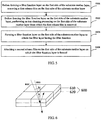
- the stray light may be filtered out by the principle of the total reflection. If part of the stray light is still not filtered out and remains in the first reflective film group, the part of the stray light will produce a light trapping effect due to a structure formed by the first reflection film layer group and the spacer film layer group and a structure formed by the spacer film layer group and the second reflection film layer group, so that the part of stray light cannot reach the photosensitive imaging device to be imaged.
- the filter film with a multi-film layer group structure realizes the filtering function by the principle of the total reflection and the light trapping effect.
- the filtering function layer which is composed of multi-film layer group further enhances the filtering function. In the case where more stray light is filtered out, effective light reaching the photosensitive imaging device will increase, thereby further improving the accuracy of the fingerprint recognition.
- the method further includes step S504, attaching a second release film on the first side of the substrate mother layer on which the filtering function layer is formed to obtain the filter layer with the filtering function.
- a release film may be attached to the first side surface of the substrate mother layer, and then the filter layer with the filtering function, which is obtained, may be curled into the roll, for storage and transportation, etc.
- the second release film is attached on the first side after forming the filtering function layer, which may prevent water, oxygen, and charged ions, and prolong service life of the filtering function layer.
- the filter layer may be provided to a manufacturing factory of a display device.
- the second release film is cut to an appropriate size for forming a back side of the display panel and using as a bottom layer film of the display panel, which is configured to provide support and protection for the display panel.
- the pixel unit array is peeled off as a whole, transferred onto the bottom layer film, and combined with the bottom layer film.
- the manufacturing method of a filter layer of forming a display device in the case where the manufacture method is used to manufacture a display device, reduces attaching processes between components and improves the assembly yield of each component. And attaching a filtering function layer on the prism is not necessary, thereby avoiding problems, such as light leakage and warpage, etc., of the filtering function layer, and thereby improving the accuracy of the fingerprint recognition. And because the filter layer has a filtering function, additionally attaching the filtering function layer on the fingerprint recognition module is not necessary any more, thereby reducing the overall thickness of the fingerprint recognition module.
Landscapes
- Engineering & Computer Science (AREA)
- General Engineering & Computer Science (AREA)
- Theoretical Computer Science (AREA)
- Inorganic Chemistry (AREA)
- Chemical & Material Sciences (AREA)
- Human Computer Interaction (AREA)
- Physics & Mathematics (AREA)
- General Physics & Mathematics (AREA)
- Sustainable Development (AREA)
- Life Sciences & Earth Sciences (AREA)
- Devices For Indicating Variable Information By Combining Individual Elements (AREA)
- Electroluminescent Light Sources (AREA)
- Image Input (AREA)
Abstract
Description
- The embodiments of the present disclosure relate to a display device and a manufacturing method thereof.
- Fingerprint recognition technology is widely used in fields of security and smart attendance, such as fingerprint punch-in, etc., and with the maturity and convenience of the technology, the fingerprint recognition technology is gradually used in smart phone terminals, and becomes a basic configuration of smart phones. With the development of full screen technology, optical fingerprint recognition solutions have been developing rapidly. How to design and manufacture a more optimized display device structure is a focus issue in the related art.
- At least one embodiment of the present disclosure provides a display device, and the display device includes a display panel and a photosensitive imaging device, wherein the display panel includes a display side and a back side opposite to the display side, and the display panel further includes a filter layer disposed at the back side of the display panel, and the photosensitive imaging device is stacked with the display panel and located at a side of the filter layer facing away from the display side, and the photosensitive imaging device is configured to detect a skin texture image of a user touching the display panel.
- For example, in the display device according to one embodiment of the present disclosure, the filter layer includes a substrate layer and a filtering function layer having a filtering function, and the substrate layer and the filtering function layer are stacked and combined with each other.
- For example, in the display device according to one embodiment of the present disclosure, a projection of the photosensitive imaging device on the substrate layer is located within a projection of the filtering function layer on the substrate layer in a direction perpendicular to the display panel.
- For example, in the display device according to one embodiment of the present disclosure, the filtering function layer includes one or more of an infrared light filtering function layer, an ultraviolet light filtering function layer, a visible light filtering function layer, and a far infrared light filtering function layer.
- For example, in the display device according to one embodiment of the present disclosure, the photosensitive imaging device includes a prism film, and the prism film is disposed at a light incident side of the photosensitive imaging device.
- For example, in the display device according to one embodiment of the present disclosure, the photosensitive imaging device is combined with the filter layer by the prism film, so that the photosensitive imaging device is stacked with the display panel and located at the side of the filter layer facing away from the display side.
- For example, in the display device according to one embodiment of the present disclosure, the filter layer has the filtering function as a whole.
- For example, in the display device according to one embodiment of the present disclosure, the display panel includes a pixel unit, the pixel unit includes a light-emitting device, and the display panel is configured to allow light emitted by the light-emitting device, in a case where the light-emitting device is working, to be reflected by a user skin touching the display panel, for skin texture image recognition.
- At least one embodiment of the present disclosure provides a manufacturing method of a display device, and the manufacturing method includes: providing a display panel, the display panel including a display side and a back side opposite to the display side, and the display panel further including a filter layer disposed at the back side of the display panel, and providing a photosensitive imaging device, the photosensitive imaging device being sequentially stacked with the display panel and located at a side of the filter layer facing away from the display side, wherein the photosensitive imaging device is configured to detect a skin texture image of a user touching the display panel.
- For example, in the manufacturing method of a display device according to one embodiment of the present disclosure, the filter layer includes a substrate layer and a filtering function layer having a filtering function, and the substrate layer and the filtering function layer are stacked and combined with each other.
- For example, in the manufacturing method of a display device according to one embodiment of the present disclosure, the filtering function layer includes one or more of an infrared light filtering function layer, an ultraviolet light filtering function layer, a visible light filtering function layer, and a far infrared light filtering function layer.
- For example, in the manufacturing method of a display device according to one embodiment of the present disclosure, the photosensitive imaging device includes a prism film, and the prism film is disposed at a light incident side of the photosensitive imaging device.
- For example, in the manufacturing method of a display device according to one embodiment of the present disclosure, the photosensitive imaging device is combined with the filter layer by the prism film, so that the photosensitive imaging device is stacked with the display panel and located at the side of the filter layer facing away from the display side.
- At least one embodiment of the present disclosure further provides a filter layer of forming a display device, and the filter layer has a filtering function.
- For example, in the filter layer of forming the display device according to one embodiment of the present disclosure, the filter layer having a filtering function includes a substrate layer and a filtering function layer having a filtering function, which are stacked and combined with each other.
- For example, in the filter layer of forming the display device according to one embodiment of the present disclosure, the filtering function layer includes one or more of an infrared light filtering function layer, an ultraviolet light filtering function layer, a visible light filtering function layer, and a far infrared light filtering function layer.
- For example, in the filter layer of forming the display device according to one embodiment of the present disclosure, the filter layer has the filtering function as a whole.
- At least one embodiment of the present disclosure further provides a manufacturing method of a filter layer having a filtering function, and the method includes: forming a filtering function layer on a first side of a substrate mother layer to obtain the filter layer having a filtering function. The manufacturing method of the filter layer may be used for manufacturing the filter layer used in the above display device
- For example, in the manufacturing method of the filter layer having the filtering function according to one embodiment of the present disclosure, the method further includes: before forming the filtering function layer on the first side of the substrate mother layer, removing a first release film on the first side of the substrate mother layer; and attaching a second release film on the first side of the substrate mother layer on which the filtering function layer is formed.
- For example, in the manufacturing method of the filter layer having the filtering function according to one embodiment of the present disclosure, the method further includes: before forming the filtering function layer on the first side of the substrate mother layer, performing an ion cleaning processing on the first side of the substrate mother layer from which the first release film is removed.
- For example, in the manufacturing method of the filter layer having the filtering function according to one embodiment of the present disclosure, forming the filtering function layer on the first side of the substrate mother layer includes: depositing the filtering function layer or attaching the filtering function layer on the first side of the substrate mother layer.
- For example, in the manufacturing method of the filter layer having the filtering function according to one embodiment of the present disclosure, the filtering function layer includes at least one film layer group, each film layer group includes a plurality of film layers, and forming the filtering function layer further includes: sequentially forming the plurality of film layers of the at least one film layer group.
- For example, in the manufacturing method of the filter layer having the filtering function according to one embodiment of the present disclosure, the filtering function layer includes a first reflection film layer group, and the first reflection film layer group includes at least one film layer having a first refractive index and at least one film layer having a second refractive index, which are disposed at intervals, and the first refractive index is greater than the second refractive index.
- For example, in the manufacturing method of the filter layer having the filtering function according to one embodiment of the present disclosure, the filtering function layer further includes a spacer film layer group and a second reflection film layer group, the first reflection film layer group, the spacer film layer group, and the second reflection film layer group are sequentially stacked on the first side of the substrate mother layer, and the second reflection film layer group includes at least one film layer having the first refractive index and at least one film layer having the second refractive index, and the spacer film layer includes a plurality of film layers with a same refractive index.
- For example, in the manufacturing method of the filter layer having the filtering function according to one embodiment of the present disclosure, a material of the film layer having the first refractive index includes Ge or PbTe, and a material of the film layer having the second refractive index includes ZnS, ZnSe, TiO2 or SiO2.
- For example, in the manufacturing method of the filter layer having the filtering function according to one embodiment of the present disclosure, a material thickness of the film layer having the first refractive index is 300 to 500 nanometers, and a material thickness of the film layer having the second refractive index is 1000 to 2000 nanometers.
- For example, in the manufacturing method of the filter layer having the filtering function according to one embodiment of the present disclosure, the first refractive index is 4 to 6, and the second refractive index is 1.3 to 2.3.
- In order to clearly illustrate the technical solution of the embodiments of the present disclosure, the drawings of the embodiments will be briefly described in the following; it is obvious that the following described drawings are only related to some embodiments of the present disclosure, and thus are not limitative of the present disclosure.
-
FIG. 1A is a schematic cross-sectional diagram of a display device according to some embodiments of the present disclosure; -
FIG. 1B is a schematic plan diagram of a display panel according to the embodiments; -
FIG. 1C is a schematic cross-sectional diagram of another display device according to the embodiments; - FIG. ID is a schematic cross-sectional diagram of still another display device according to the embodiments;
-
FIG. 2 is a schematic cross-sectional diagram of another display device according to some embodiments of the present disclosure; -
FIG. 3 is a block diagram of still another display device 300 according to some embodiments of the present disclosure; -
FIG. 4 is a schematic flowchart of a manufacturing method of a display device according to some embodiments of the present disclosure; -
FIG. 5 is a schematic flowchart of a manufacturing method of a filter layer with a filtering function according to some embodiments of the present disclosure; -
FIG. 6 is a schematic diagram of a layer structure of a filtering function layer according to some embodiments of the present disclosure; -
FIG. 7A is a schematic diagram of a layer structure of another filtering function layer according to some embodiments of the present disclosure; -
FIG. 7B is a schematic diagram of a layer structure of still another filtering function layer according to some embodiments of the present disclosure. - In order to make objects, technical solutions and advantages of the embodiments of the present disclosure apparent, the technical solutions of the embodiments of the present disclosure will be described in a clearly and fully understandable way in connection with the accompanying drawings related to the embodiments of the present disclosure. Apparently, the described embodiments are just a part but not all of the embodiments of the present disclosure. Based on the described embodiments of the present disclosure, those skilled in the art can obtain other embodiment(s), without any inventive work, which should be within the scope of the present disclosure.
- Unless otherwise defined, all the technical and scientific terms used herein have the same meanings as commonly understood by one of ordinary skill in the art to which the present disclosure belongs. The terms "first," "second," etc., which are used in the present disclosure, are not intended to indicate any sequence, amount or importance, but distinguish various components. Further, the terms such as "a," "an," "the," etc., are not intended to limit the amount, but indicate the existence of at least one. The terms "comprise," "comprising," "include," "including," etc., are intended to specify that the elements or the objects stated before these terms encompass the elements or the objects and equivalents thereof listed after these terms, but do not preclude the other elements or objects. The phrases "connect", "connected", etc., are not intended to define a physical connection or mechanical connection, but may include an electrical connection, directly or indirectly. "On," "under," "right," "left" and the like are only used to indicate relative position relationship, and when the position of the object which is described is changed, the relative position relationship may be changed accordingly.
- A display device with an optical fingerprint recognition solution includes a filtering function layer, a prism film, and a photosensitive imaging device which are sequentially stacked and attached to a back side of a display panel, light-emitting units of the display device are configured to emit light upward, and the light emitted by the light-emitting units is reflected back by a finger and is collected and imaged in the photosensitive imaging device after filtering out interference light by the filtering function layer. Because the reflectivity of the light on ridges of the finger is different from that of the light on valleys of the finger, fingerprint recognition can be realized, and an image comparison and algorithm processing, etc., may be performed in a processing chip integrated in the photosensitive imaging device or an external processing chip.
- In the above display device, the filtering function layer, the prism film, and the photosensitive imaging device are required to be sequentially attached on the back side of the display panel, and there are many attaching processes between components. Moreover, in the case where the filtering function layer is attached on the prism film, due to insufficient sealing at edges, problems, such as light leakage and warpage, etc., of the filtering function layer may occur, which may make the fingerprint recognition invalid, make the assembly yield of each component not high, and make a reducible space of an overall thickness of a fingerprint recognition module (including the filtering function layer, the prism film, and the photosensitive imaging device) extremely limited.
- At least one embodiment of the present disclosure provides a display device, and the display device includes a display panel and a photosensitive imaging device. The display panel includes a display side and a back side opposite to the display side, and the display panel further includes a filter layer disposed at the back side of the display panel. The photosensitive imaging device is stacked with the display panel and located at a side of the filter layer facing away from the display side, and the photosensitive imaging device is configured to detect a skin texture image of a user touching the display panel.
- At least one embodiment of the present disclosure provides the display device and a manufacturing method of the display device, the display panel in the display device includes the filter layer having the filtering function, and the photosensitive imaging device is stacked with the display panel and located at the side of the filter layer facing away from the display side, which reduces attaching processes between components and improves the assembly yield of each component, and attaching the filtering function layer on the prism becomes unnecessary, thereby avoiding the problems, such as light leakage and warpage, etc., of the filtering function layer, which improves the accuracy of the fingerprint recognition, and because the filter layer has a filtering function, additionally attaching the filtering function layer on the fingerprint recognition module becomes unnecessary, thereby reducing the overall thickness of the fingerprint recognition module.
- Hereinafter, the embodiments of the present disclosure will be described in detail with reference to the accompanying drawings. It should be noted that same or similar reference numerals in different drawings will be used to refer to the same elements that have been described.
- FIG. lAis a schematic cross-sectional diagram of a
display device 100 according to some embodiments of the present disclosure;FIG. 1B is a schematic plan diagram of adisplay panel 110 according to the embodiments;FIG. 1C is a schematic cross-sectional diagram of anotherdisplay device 100 according to the embodiments; and FIG. ID is a schematic cross-sectional diagram of still anotherdisplay device 100 according to the embodiments. - Referring to
FIG. 1A and FIG. 1B , thedisplay device 100 includes adisplay panel 110 and aphotosensitive imaging device 130. Thedisplay panel 110 includes adisplay side 111 and aback side 112 opposite to the display side, and further includes afilter layer 120 disposed at theback side 112 of the display panel. Thephotosensitive imaging device 130 is stacked with thedisplay panel 110 and located at a side of thefilter layer 120 facing away from thedisplay side 111. In addition, thedisplay panel 110 and thephotosensitive imaging device 130 are sequentially stacked, and thephotosensitive imaging device 130 is located in adisplay area 1111 of thedisplay panel 110 and located on the back side of thedisplay panel 110. Therefore, the display device integrates a display function and an under-screen skin texture recognition function. For example, the filter layer functions as a bottom layer film (for example, a base substrate) of thedisplay panel 110, that is, thedisplay panel 110 has a bottom layer film with a filtering function, which filters out the interference light from the light incident on the display side during operations, so that the light reflected by the skin texture is collected and imaged on the photosensitive imaging device, thereby improving imaging quality and improving fingerprint recognition effect. - The
display panel 110 may be an organic light-emitting diode (OLED) display panel, or may be an electronic paper display panel, which is not limited in the embodiments of the present disclosure. The OLED display panel may be, for example, a flexible OLED display panel. The OLED display panel has self-luminous characteristics, and the light emitted by the display pixel units of the OLED display panel can further be controlled or modulated as desired, thereby providing convenience for fingerprint image collection, and contributing to improve the integration level of the electronic device. - As shown in
FIG. 1A and FIG. 1B , thedisplay panel 110 includes thedisplay side 111 having adisplay area 1111 and theback side 112 opposite to the display side. Thedisplay area 1111 includes afingerprint recognition area 1112. Thefingerprint recognition area 1112 may be part or all of thedisplay area 1111, thereby realizing a partial under-screen fingerprint recognition function or a full under-screen fingerprint recognition function. The user can put his/her finger in thefingerprint recognition area 1112 or press upon thefingerprint recognition area 1112. When a light-emitting unit of the display device emits light, the light emitted by the light-emitting unit is reflected back by the finger, and is collected and imaged on thephotosensitive imaging device 130. Then a fingerprint image obtained by thephotosensitive imaging device 130 can be subsequently used for a fingerprint recognition operation. - The
photosensitive imaging device 130 may be configured to collect skin texture images of a user, such as fingerprint images and palm print images, etc., and thus the skin texture images of the user may be used for realizing functions such as fingerprint recognition and palm print recognition, etc. Thephotosensitive imaging device 130 has a certain working area (an active area), and includes a plurality of pixel units that are arranged in a predetermined array. Thephotosensitive imaging device 130 is coupled to a processor (for example, an integrated circuit chip) by, for example, a lead(s), so that the collected fingerprint image may be transmitted to the processor in a data signal manner. Thephotosensitive imaging device 130 may be various suitable types of fingerprint sensors, such as a charge coupled device (CCD) type image sensor, a complementary metal oxide semiconductor (CMOS) type image sensor, etc. According to requirements, thephotosensitive imaging device 130 may, for example, sense only light of a certain wavelength (for example, red light or green light), or may sense all visible light. The following specific example will be described by taking that thephotosensitive imaging device 130 is configured as a fingerprint sensor for fingerprint recognition as an example. - As shown in
FIG. 1A , thefilter layer 120 having the filtering function is disposed between thephotosensitive imaging device 130 and the back side of thedisplay panel 110, and is configured to support the pixel unit array of thedisplay panel 110. The pixel unit array may be directly manufactured on thefilter layer 120. In this structure, when the display panel emits light, for example, the light-emitting device of thedisplay panel 110 itself can be made to emit light, or an external light source (such as a backlight) can further be provided to enable thedisplay panel 110 to emit light, after the finger reflects back the light emitted by thelight panel 110, the interference light (such as infrared light) is filtered out by thefilter layer 120 having the filtering function, so that the reflected light, which has been subjected to filtering, reaches thephotosensitive imaging device 130, and is collected and imaged on thephotosensitive imaging device 130. Then the fingerprint image obtained by thephotosensitive imaging device 130 may be used for subsequent fingerprint recognition operations. - In this example, for example, the
filter layer 120 having the filtering function is provided as the back side of thedisplay panel 110, and thephotosensitive imaging device 130 is attached to the back side (that is, a side opposite to the pixel unit array) of thefilter layer 120 having the filtering function with a double-sided tape or an adhesive, so that thefilter layer 120 and thephotosensitive imaging device 130 are stacked on the back side of thedisplay panel 110. Of course, thefilter layer 120 and thephotosensitive imaging device 130 may be fixed to each other in other ways. - In the above structure, the
filter layer 120 having the filtering function is of a single body which is manufactured with the filtering function in advance, for example, the filter layer, which is of a single body, is formed by depositing the filtering function layer on a substrate mother layer in advance (the manufacturing process of the filter layer will be described in detail later). Because the filter layer has the filtering function as a whole, the process of attaching the filtering function layer on the prism can be omitted, and the thickness of the fingerprint recognition module and the thickness of the entire display device can be reduced. - In another example, as shown in
FIG. 1C , thefilter layer 120 having the filtering function may not be of a single body, which is manufactured with the filtering function in advance, but may include asubstrate layer 121 and afiltering function layer 122 having the filtering function, which are stacked and attached with each other. In this example, thesubstrate layer 121 supports the pixel unit array of thedisplay panel 110, thefiltering function layer 122 may be attached to thesubstrate layer 121 by a double-sided tape or an adhesive, and thephotosensitive imaging device 130 may be attached to the back side of thefiltering function layer 122 by a double-sided tape or an adhesive, so that thesubstrate layer 121, thefiltering function layer 122 and thephotosensitive imaging device 130 are stacked on the back side of thedisplay panel 110. Similarly, thesubstrate layer 121, thefiltering function layer 122 having the filtering function, and thephotosensitive imaging device 130 may be fixed to each other in other ways. - Please refer to
FIG 1C , in the direction perpendicular to thedisplay panel 110, thefiltering function layer 122 partially or completely covers the bottom of thesubstrate layer 121, and the projection of thephotosensitive imaging device 130 on thesubstrate layer 121 is located within the projection of thefiltering function layer 122 on thesubstrate layer 121. For example, the size of the projection of thefiltering function layer 122 on thesubstrate layer 121 may be equal to the size of thesubstrate layer 121, for example, thefiltering function layer 122 and thesubstrate layer 121 are obtained by the same cutting process as described below, and the size of the projection of thephotosensitive imaging device 130 on thesubstrate layer 121 is smaller than the size of thesubstrate layer 121. - By attaching the filtering function layer on the substrate layer, and locating the projection of the photosensitive imaging device on the substrate layer within the projection of the filtering function layer on the substrate layer, problems of the filtering function layer, such as light leakage and warpage, etc., which are cause by the insufficient sealing at edges, in the case where the filtering function layer is attached on the prism, may be avoided. In the case where the problem of light leakage of the filtering function layer is alleviated, more stray light may be effectively filtered out, thereby further improving the accuracy of the fingerprint recognition.
- Because infrared light has a strong penetrating ability and cannot form reflections at ridges and valleys of a finger, infrared light belongs to stray light and can reduce a signal-to-noise ratio and affect imaging quality. Therefore, in this example, the
filtering function layer 122 may be an infrared light filtering function layer for filtering infrared stray light. Of course, thefiltering function layer 122 may be implement in more than one way. For example, thefiltering function layer 122 may include one or more of an infrared light filtering function layer, an ultraviolet light filtering function layer, a visible light filtering function layer, and a far infrared light filtering function layer. In different application scenarios, by setting the filtering function layer to filter out different types of stray light, the application scenarios of the embodiments of the present disclosure are more extensive. - In another example, as shown in FIG. ID, the
photosensitive imaging device 130 may include aprism film 131, and theprism film 131 is disposed at alight incident side 151 of thephotosensitive imaging device 130. In this example, thephotosensitive imaging device 130 is combined with thefilter layer 120 by theprism film 131, for example, thefilter layer 120 and theprism film 131 are combined by adhering to each other, so that thephotosensitive imaging device 130 is stacked with thedisplay panel 110 and located at the side of thefilter layer 120 facing away from thedisplay side 111. - In this exemplary structure, when the display panel emits light, for example, the light-emitting device of the
display panel 110 itself can be made to emit light, or an external light source (such as a backlight) can further be provided to enable thedisplay panel 110 to emit light, after the finger reflects back the light emitted by thelight panel 110, the interference light is filtered out by thefilter layer 120 having the filtering function, so that the reflected light, which has been subjected to the filtering, reaches theprism film 131, theprism film 131 brightens the filtered reflected light, and then the light that has been brightened is transmitted to the photosensitive imaging device 130 (for example, a sensor) for imaging. Then the fingerprint image obtained by thephotosensitive imaging device 130 can be used for a subsequent fingerprint recognition operation. - In this example, the
photosensitive imaging device 130 may be attached to a back side of theprism film 131 by a double-sided tape, and theprism film 131 may be attached to the back side of thefilter layer 120 by a double-sided tape, so that thephotosensitive imaging device 130, theprism film 131, and thefilter layer 120 are stacked on the back side of thedisplay panel 110. Similarly, thefilter layer 120, theprism film 131, and thephotosensitive imaging device 130 may be fixed to each other by other ways. - In some embodiments, the
display device 100 further includes aback plate 140 which is configured to provide support and protection for thedisplay device 100. For example, the stacked structure of thefilter layer 120 and thephotosensitive imaging device 130 may further directly or indirectly abut on theback plate 140, and may be relatively fixed on theback plate 140. - Of course, the structure of the
display device 100 according to any of the embodiments of the present disclosure is not limited to the exemplary structures as shown inFIG. 1A - FIG. 1D . For example, thedisplay device 100 may further include other devices, such as a driving chip, a memory, a microphone, a speaker, etc., which will not be described in detail here. - At least one embodiment of the present disclosure provides a display device, a display panel of the display device includes a filter layer having a filtering function, and a photosensitive imaging device is stacked with the display panel and located at a side of the filter layer facing away from the display side, which reduces attaching processes between components and therefore improves the assembly yield of each component. Moreover, in these embodiments, attaching the filtering function layer on the prism of the photosensitive imaging device becomes unnecessary, thereby avoiding problems, such as light leakage and warpage, etc., of the filtering function layer, and thereby improving the accuracy of the fingerprint recognition. In addition, because the filter layer has a filtering function, additionally attaching the filtering function layer on the fingerprint recognition module is not necessary, thereby reducing the overall thickness of the fingerprint recognition module. For example, the filter layer functions as a bottom layer film of the display panel, and is disposed at the back side of the display panel.
-
FIG. 2 is a schematic cross-sectional diagram of anotherdisplay device 200 according to some embodiments of the present disclosure. Referring to the embodiment ofFIG. 2 , thedisplay device 200 includes adisplay panel 210 and aphotosensitive imaging device 230. In the present embodiment, thedisplay panel 210 is an OLED display panel. - As shown in
FIG. 2 , theOLED display panel 210 includes atop film 201, athin film package 202, apixel unit array 203, a flexible substrate 204, afiltering function layer 205, and a bottom layer film 206, etc. In the display panel, the stack of thefiltering function layer 205 and the bottom layer film 206, as a whole, provides a filter layer having a filtering function, and functions as a bottom layer film of the display panel, which is located on a back side of the display panel, specifically, which is a side opposite to thepixel unit array 203 on the flexible substrate 204. - The bottom layer film 206 provides a protection and support function for other structures and functional layers thereon, and the bottom layer film 206 may be, for example, a stronger plastic substrate or a plastic substrate or a glass substrate with a higher strength. The
filtering function layer 205 is located on the bottom layer film 206 for filtering out the stray light. Thefiltering function layer 205 may include one or more of an infrared light filtering function layer, an ultraviolet light filtering function layer, a visible light filtering function layer, and a far infrared light filtering function layer. The flexible substrate 204 is configured to provide a buffer, such as a flexible substrate made of a material such as polyimide (PI), polypropylene (PP), polycarbonate (PC), etc. - The
pixel unit array 203 is formed on the flexible substrate 204, and includes a plurality of pixel units arranged in a predetermined array and signal lines (including gate lines, data lines, detection lines, etc.) for providing electrical signals (including scanning signals, data signals, detection signals, etc.). Each pixel unit includes a light-emitting device (for example, an OLED device) and a pixel driving circuit for driving the light-emitting device (the OLED device) to emit light, etc. The pixel driving circuit is coupled to the signal line, so that the pixel driving circuit can receive a corresponding control signal and a driving voltage, and drive the light-emitting device to emit light as requirements, thereby performing functions such as display, touching sensing, or skin texture (such as fingerprint) recognition, etc.Light 101 emitted by the pixel units may be used for displaying, and also used as incident light for the under-screen fingerprint detection. Specifically, the light 101 emitted by the light-emitting devices in the pixel units, when the light-emitting device is working, is reflected by a user's skin (a finger or a palm) 250 on the display side of the display panel for the skin texture image recognition of the user. - The
thin film package 202 covers thepixel unit array 203 to prevent outside water vapor from entering thepixel unit array 203 to cause aging or deterioration. Thethin film package 202 may be a multilayer thin film package, for example, including a stacked inorganic insulating layer and an organic insulating layer, etc. - The
top film 201 may be a cover plate, such as a substrate or a thick film made of glass or plastic, and is configure to provide support and protection, for example, for the user to perform operations such as touching, pressing, etc. - According to requirements, the
OLED display panel 210 may further include other structures or functional layers. For example, theOLED display panel 210 may include a touch structure for realizing a touch function. The touch structure may be built in thepixel unit array 203, or formed on the top film, and the touch structure may be in, for example, a capacitive type, a resistive type, etc. - In order to realize the under-screen fingerprint detection function, the
top film 201, thethin film package 202, the flexible substrate 204, thefiltering function layer 205, and the bottom layer film 206, which are described above, are at least partially transparent. The light 101 (indicated by a solid arrow) emitted by the light-emitting device in the pixel unit, in a case where the light-emitting device is working, is reflected by the skin (a finger or a palm) 250 of the user on the display side of the display panel, and the reflected light (indicated by a dashed arrow) may be incident on thephotosensitive imaging device 230, so that thephotosensitive imaging device 230 may form an image, and the image, which is obtained, is used to implement subsequent fingerprint recognition operations. Thephotographic imaging device 230 may include aprism film 220, and theprism film 220 is disposed at a light incident side of thephotosensitive imaging device 230. Thephotosensitive imaging device 230 is combined with the bottom layer film 206 by theprism film 220, so that thephotosensitive imaging device 230 is stacked with thedisplay panel 210, and disposed at a side of the bottom layer film 206 of the display panel facing thephotosensitive imaging device 230. The light reflected by the skin (the finger or the palm) 250 of the user on the display side of the display panel is incident on thephotosensitive imaging device 230 by theprism film 220. - In at least one embodiment of the present disclosure, in order to use the principle of pinhole imaging to improve the effect of the
photosensitive imaging device 230, a pinhole(s) may further be formed in the layer structure as shown inFIG. 2 (for example, a pinhole layer including a pinhole(s) is provided separately), and the pinhole(s) corresponds to thephotosensitive imaging device 230. - The display device according to at least one embodiment of the present disclosure reduces attaching processes between components and improves the assembly yield of each component.
-
FIG. 3 is a block diagram of still another display device 300 according to some embodiments of the present disclosure, the display device is, for example, a mobile phone or a tablet computer. As shown inFIG. 3 , the display device 300 includes adisplay panel 310, atouch structure 320, aphotosensitive imaging device 330, acontroller 340 and afingerprint processor 350. The ways to implementdisplay panel 310 and thephotosensitive imaging device 330 are the same as those of thedisplay panel 110 and thephotosensitive imaging device 130 in the above embodiments, and details are not described herein again. Thetouch structure 320 is coupled to thedisplay panel 310, thephotosensitive imaging device 330, and thecontroller 340, respectively. Thecontroller 340 is coupled to thedisplay panel 310, thetouch structure 320, thephotosensitive imaging device 330, and thefingerprint processor 350, respectively. - In some embodiments, when the
touch structure 320 senses a user's pressing action on a display side of thedisplay panel 310, thetouch structure 320 transmits a feedback signal to thecontroller 340. The feedback signal may include information that thedisplay panel 310 is pressed by a user, and may further include information such as a pressing degree (level), a pressing position, etc. - The
controller 340 receives the feedback signal transmitted by thetouch structure 320. Thecontroller 340 controls thedisplay panel 310 to emit light, that is, to light up the screen. Under this case, thecontroller 340 further controls thephotosensitive imaging device 330 to start to collect a fingerprint image(s) and transmit the fingerprint image(s) to thefingerprint processor 350 for fingerprint recognition (and verification) of the user. After that, thefingerprint processor 350 transmits a recognition result to thecontroller 340, and thecontroller 340 performs subsequent (predetermined) operations according to the fingerprint recognition result. In a case where thecontroller 340 controls thedisplay panel 310 to emit light to light up the screen, for example, a system of a mobile phone or a tablet is in a standby state, it is waited for a user to enter a password, etc., to unlock the system. Accordingly, in the case where the fingerprint recognition is successful, thecontroller 340 controls the system of the mobile phone or the tablet to enter into a working state, for example, an operation interface of an application before being in an off-screen state is displayed. The embodiments of the present disclosure are not limited thereto. - As a modified embodiment, the
photosensitive imaging device 330 may transmit the fingerprint image imaged thereon to thecontroller 340, and thecontroller 340 transmits the user fingerprint image to thefingerprint processor 350, so that thefingerprint processor 350 completes the texture image recognition of the user. For example, if the texture recognition of the user is successful, thecontroller 340 releases a system lock state of an electronic device including the display device. If the texture recognition of the user or verification fails, thecontroller 340 controls thedisplay panel 310 not to emit light, i.e., makes thedisplay device 100 remain in the off-screen state. - In some embodiments of the present disclosure, the fingerprint processor may be implemented by a general-purpose processor or a special-purpose processor. The controller may be various types of integrated circuit chips with processing functions, which may have various computing architectures, such as a complex Instruction Set Computer (CISC) structure, a Reduced Instruction Set Computer (RISC) structure, or a structure that implements a combination of multiple instruction sets. In some embodiments, the controller may be a microprocessor, such as an X86 processor or an ARM processor, or may be a digital processor (DSP), etc.
- Other embodiments of the present disclosure provide a manufacturing method of the display device described above, and the manufacturing method and a working principle of the display device according to at least one embodiment of the present disclosure will be exemplarily described below with reference to
FIG. 4 . - At step S401, a display panel is provided, the display panel includes a display side and a back side opposite to the display side, and the display panel further includes a filter layer disposed at the back side of the display panel.
- The display panel may be any display panel in the above embodiments, and details are not described herein again.
- At step S402, a photosensitive imaging device is provided, the photosensitive imaging device are sequentially stacked with the display panel and located at a side of the filter layer facing away from the display side, and the photosensitive imaging device is configured to detect a skin texture image of the user touching the display panel.
- The filter layer having the filtering function may be a filter layer as a single body, which is manufactured in advance, for example, it may be used as a bottom layer film of the display panel, that is, the filter layer as a whole has the filtering function, or may include a substrate layer and a filtering function layer having a filtering function, which are stacked and attached to each other. Further, for example, the filtering function layer may include one or more of an infrared light filtering function layer, an ultraviolet light filtering function layer, a visible light filtering function layer, and a far infrared light filtering function layer.
- The photosensitive imaging device may include a prism film, and the method further includes step S403. The prism film is disposed at a light incident side of the photosensitive imaging device. The photosensitive imaging device may be combined with the filter layer by the prism film, so that the photosensitive imaging device is stacked with the display panel and located at the side of the filter layer facing away from the display side.
- For the specific implementation process of the above steps may further refer to the description of the above embodiments of the display device, and details are not described herein again.
- A manufacturing method of a display device according to at least one embodiment of the present disclosure may reduce attaching processes between components and improve the assembly yield of each component. And attaching a filtering function layer on the prism becomes unnecessary, thereby avoiding problems, such as light leakage and warpage, etc., of the filtering function layer, and thereby improving the accuracy of the fingerprint recognition. And because the filter layer has a filtering function, additionally attaching the filtering function layer on the fingerprint recognition module is not necessary, thereby reducing the overall thickness of the fingerprint recognition module.
- Other embodiments of the present disclosure further provide a filter layer for forming a display device. The filter layer may be used in the display device in the above embodiments, and the filter layer has a filtering function.
- The filter layer having the filtering function may be the filter layer having the filtering function as a whole, which is manufactured in advance, that is, the filter layer as a whole has the filtering function, or may include a substrate layer and the filtering function layer having the filtering function, which are stacked and attached with each other. Further, for example, the filtering function layer may include one or more of an infrared light filtering function layer, an ultraviolet light filtering function layer, a visible light filtering function layer, and a far infrared light filtering function layer.
- The filter layer for forming the display device according to at least one embodiment of the present disclosure, in the case where the filter layer is used in the display device, attaching processes between components is reduced and the assembly yield of each component is improved. And attaching a filtering function layer on the prism is not necessary any more, thereby avoiding problems, such as light leakage and warpage, etc., of the filtering function layer, and thereby improving the accuracy of the fingerprint recognition. Because the filter layer has a filtering function, additionally attaching the filtering function layer on the fingerprint recognition module is not necessary, thereby reducing the overall thickness of the fingerprint recognition module.
- Another embodiment of the present disclosure provides a manufacturing method of the filter layer having the filtering function, which is mentioned above, and the manufacturing method of the filter layer may be used for manufacturing the filter layer used in the display device, and the method includes: forming a filtering function layer on a first side of a substrate mother layer to obtain the filter layer having the filtering function.
- Hereinafter, the manufacturing method and the working principle of the filter layer having the filtering function according to at least one embodiment of the present disclosure will be exemplarily described below with reference to
FIG 5 . - At step S501, before forming a filtering function layer on the first side of the substrate mother layer, a first release film on the first side of the substrate mother layer is removed.
- For example, the substrate mother layer may be a roll of PET (Polyethylene terephthalate), PMMA (poly (methyl methacrylate)), etc. In order to realize curling into the roll, a release film is usually attached to one or both sides of the substrate mother layer. In order to form the filtering function layer on the first side of the substrate mother layer, the first release film of the substrate mother layer is removed at first, which makes the filtering function layer be better attached to the substrate mother layer.
- At step S502, before forming the filtering function layer on the first side of the substrate mother layer, an ion cleaning processing is performed on the first side of the substrate mother layer, from which the first release film is removed.
- Performing the ion cleaning processing on the first side of the substrate mother layer may further remove organic objects (such as the previously used adhesive) attached to the surface of the first side, so that the filtering function layer may be better attached to the substrate mother layer.
- At step S503, a filtering function layer is formed on the first side of the substrate mother layer to obtain the filter layer having the filtering function.
- In the case where the light emitted from the display panel and reflected by user skin or light incident from outside may form stray light in a large viewing angle, which will affect a recognition result of the skin texture of the user by the photosensitive imaging device. Therefore, it is necessary to filter out the stray light by the filtering function layer.
- There implementation methods of forming the filtering function layer on the first side of the substrate mother layer are many. For example, the filtering function layer may be formed by using a material having an adsorption effect on a certain type of light, or the filtering function layer may be formed by setting a film layer structure of the filtering function layer (for example, selecting refractive indexes of mediums on both sides of an interface on a light incident path to filter out stray light). For example, the filtering function layer may include at least one film layer group, each film layer group includes a plurality of film layers, and the filtering function layer is formed by sequentially forming the plurality of film layers of the at least one film layer group.
-
FIG. 6 is a schematic diagram of a layer structure of a filtering function layer according to some embodiments of the present disclosure. Referring toFIG. 6 , the filtering function layer includes a first reflectionfilm layer group 600, the first reflectionfilm layer group 600 includes afilm layer 610 having a first refractive index and afilm layer 620 having a second refractive index disposed at intervals, and the first refractive index is greater than the second refractive index. Of course, it can be understood that the first reflectionfilm layer group 600 is not limited to the structure as shown inFIG. 6 . For example, the first reflectionfilm layer group 600 may include a plurality of (e.g., 1 to 10) film layers 610 having the first refractive index and a plurality of (e.g., 1 to 10) film layers 620 having the second refractive index. - In the present embodiment, filtering out the stray light may be implemented by controlling the film layers 610 having the first refractive index and the film layers 620 having the second refractive index in the first reflection
film layer group 600. For example, filtering out the stray light may be implemented by selecting various first refractive indexes and various second refractive indexes. The first refractive index may be set to be 4 to 6, and the second refractive index may be set to be 1.3 to 2.3. Of course, the setting of the magnitudes of the first refractive index and the second refractive index is not limited to the above embodiments. As another example, filtering out the stray light may be implemented by selecting different materials for the film layer. The material of the film layer having the first refractive index may include Ge or PbTe, and the material of the film layer having the second refractive index may include ZnS, ZnSe, TiO2 or SiO2. Similarly, the selection of the materials of the film layer having the first refractive index and the selection of the materials of the film layer having the second refractive index are not limited thereto. Still for another example, filtering out the stray light may be implemented by setting different thicknesses of the materials of the film layer. The thickness of the material of the film layer having the first refractive index may be set to be 300 to 500 nanometers, and the thickness of the material of the film layer having the second refractive index may be set to be 1000 to 2000 nanometers. Similarly, the selection of the thickness of the film layer having the first refractive index and the selection of the thickness of the film layer having the second refractive index are not limited thereto. - The refractive index may be increased by the different settings of the film layers having the first refractive index and the film layers having the second refractive index, which is described above. For example, by setting of the above parameters, high transmittance (more than 90%) for visible light at 400nm ∼ 630nm and low transmittance (less than 5%) of infrared light at 700 nm ∼ 1100nm may be achieved. In the case where the stray light is filtered out, effective light used for the photosensitive imaging device increases, thereby further improving the accuracy of the fingerprint recognition.
- In this example, in the case where the incident angle of light 6001 incident from the display side of the display panel is smaller than a total reflection angle θ1, the light 6001, which is incident, may pass through the interface between the
film layer 610 having the first refractive index of the first reflectionfilm layer group 600 and thefilm layer 620 having the second refractive index of the first reflectionfilm layer group 600, and further form an image on the photosensitive imaging device. In the case where the incident angle of light 6002 incident on the display side of the display panel is greater than θ1, because an incident angle θ2 of the light 6002 is greater than the total reflection angle θ1, the light 6002 is totally reflected at the interface between thefilm layer 610 having the first refractive index of the first reflectionfilm layer group 600 and thefilm layer 620 having the second refractive index of the first reflectionfilm layer group 600, and cannot reach the photosensitive imaging device to be imaged, thus realizing the filtering function of the filtering function layer by the principle of total reflection. -
FIG. 7A and FIG. 7B is a schematic structure of a layer structure of a filtering function layer according to another embodiment of the present disclosure. Please refer toFIGS. 7A and 7B , the filtering function layer includes a first reflectionfilm layer group 710, a spacerfilm layer group 720 and a second reflectionfilm layer group 730. The first reflectionfilm layer group 710, the spacerfilm layer group 720, and the second reflectionfilm layer group 730 are sequentially stacked on the first side of the substrate mother layer - The first reflection
film layer group 710 and the second reflectionfilm layer group 730 may include at least onefilm layer 701 having the first refractive index and at least onefilm layer 702 having the second refractive index. This setting is similar to the setting of the first reflectionfilm layer group 600 in the previous embodiment, and details are not described herein again. - The
spacer film layer 720 may include a plurality of film layers having a same refractive index, in the embodiment, the refractive index may be set to the first refractive index or the second refractive index. For example, as shown inFIG. 7A , a plurality of film layers 701 having the first refractive index may be included, or as shown inFIG. 7B , a plurality of film layers 702 having the second refractive index may be included. For related settings of the first refractive index and the second refractive index, reference may be made to the description of the corresponding embodiment ofFIG. 6 , and details are not described herein again. In addition, a number of film layers included in thespacer film layer 720 may be set as requirements, and for example, may include 1 to 10 layers. - In this example, in the case where the light incident on the display side of the display panel first reaches the first reflection film layer group, the stray light may be filtered out by the principle of the total reflection. If part of the stray light is still not filtered out and remains in the first reflective film group, the part of the stray light will produce a light trapping effect due to a structure formed by the first reflection film layer group and the spacer film layer group and a structure formed by the spacer film layer group and the second reflection film layer group, so that the part of stray light cannot reach the photosensitive imaging device to be imaged. The filter film with a multi-film layer group structure realizes the filtering function by the principle of the total reflection and the light trapping effect.
- The filtering function layer, which is composed of multi-film layer group further enhances the filtering function. In the case where more stray light is filtered out, effective light reaching the photosensitive imaging device will increase, thereby further improving the accuracy of the fingerprint recognition.
- Further referring to
FIG. 5 , the method further includes step S504, attaching a second release film on the first side of the substrate mother layer on which the filtering function layer is formed to obtain the filter layer with the filtering function. - Therefore, after forming the filtering function layer, a release film may be attached to the first side surface of the substrate mother layer, and then the filter layer with the filtering function, which is obtained, may be curled into the roll, for storage and transportation, etc. The second release film is attached on the first side after forming the filtering function layer, which may prevent water, oxygen, and charged ions, and prolong service life of the filtering function layer.
- After the filter layer having the filtering function is manufactured, the filter layer may be provided to a manufacturing factory of a display device. During a manufacturing process of the display panel, after removing the second release film on the surface of the filtering function layer of the filter layer having the filtering function, the second release film is cut to an appropriate size for forming a back side of the display panel and using as a bottom layer film of the display panel, which is configured to provide support and protection for the display panel. For example, after a pixel unit array is manufactured on a flexible substrate, the pixel unit array is peeled off as a whole, transferred onto the bottom layer film, and combined with the bottom layer film.
- The manufacturing method of a filter layer of forming a display device according to at least one embodiment of the present disclosure, in the case where the manufacture method is used to manufacture a display device, reduces attaching processes between components and improves the assembly yield of each component. And attaching a filtering function layer on the prism is not necessary, thereby avoiding problems, such as light leakage and warpage, etc., of the filtering function layer, and thereby improving the accuracy of the fingerprint recognition. And because the filter layer has a filtering function, additionally attaching the filtering function layer on the fingerprint recognition module is not necessary any more, thereby reducing the overall thickness of the fingerprint recognition module.
- The following statements should be noted:
- (1) The accompanying drawings of the embodiments of the present disclosure involve only the structure(s) in connection with the embodiment(s) of the present disclosure, and other structure(s) can be referred to common design(s).
- (2) In case of no conflict, features in one embodiment or in different embodiments can be combined.
- What are described above is related to the specific implementations of the present disclosure only and not limitative to the protection scope of the disclosure. The protection scope of the present disclosure shall be subject to that of the claims.
Claims (23)
- A display device comprising:a display panel and a photosensitive imaging device,wherein the display panel comprises a display side and a back side opposite to the display side, and the display panel further comprises a filter layer disposed at the back side of the display panel, andthe photosensitive imaging device is stacked with the display panel and located at a side of the filter layer facing away from the display side, and the photosensitive imaging device is configured to detect a skin texture image of a user touching the display panel.
- The display device according to claim 1, wherein the filter layer comprises a substrate layer and a filtering function layer having a filtering function, and the substrate layer and the filtering function layer are stacked and combined with each other.
- The display device according to claim 2, wherein a projection of the photosensitive imaging device on the substrate layer is located within a projection of the filtering function layer on the substrate layer in a direction perpendicular to the display panel.
- The display device according to claim 2 or 3, wherein the filtering function layer comprises one or more selected from the group consisting of an infrared light filtering function layer, an ultraviolet light filtering function layer, a visible light filtering function layer, and a far infrared light filtering function layer.
- The display device according to claim 1, wherein the photosensitive imaging device comprises a prism film, and the prism film is disposed at a light incident side of the photosensitive imaging device.
- The display device according to claim 5, wherein the photosensitive imaging device is combined with the filter layer by the prism film, so that the photosensitive imaging device is stacked with the display panel and located at the side of the filter layer facing away from the display side.
- The display device according to claim 1, wherein the filter layer has the filtering function as a whole.
- The display device according to claim 1, wherein the display panel comprises a pixel unit, the pixel unit comprises a light-emitting device, and
the display panel is configured to allow light emitted by the light-emitting device, in a case where the light-emitting device is working, to be reflected by a user skin touching the display panel, for skin texture image recognition. - A method of manufacturing the display device according to any one of claims 1-8, comprising:providing a display panel, the display panel comprising a display side and a back side opposite to the display side, and the display panel further comprising a filter layer disposed at the back side of the display panel, andproviding a photosensitive imaging device, the photosensitive imaging device being sequentially stacked with the display panel and located at a side of the filter layer facing away from the display side, wherein the photosensitive imaging device is configured to detect a skin texture image of a user touching the display panel.
- The method according to claim 9, wherein the filter layer comprises a substrate layer and a filtering function layer having a filtering function, and the substrate layer and the filtering function layer are stacked and combined with each other.
- The method according to claim 10, wherein the filtering function layer comprises one or more selected from the group consisting of an infrared light filtering function layer, an ultraviolet light filtering function layer, a visible light filtering function layer, and a far infrared light filtering function layer.
- The method according to claim 9, wherein the photosensitive imaging device comprises a prism film, and the prism film is disposed at a light incident side of the photosensitive imaging device.
- The method according to claim 12, wherein the photosensitive imaging device is combined with the filter layer by the prism film, so that the photosensitive imaging device is stacked with the display panel and located at the side of the filter layer facing away from the display side.
- The method according to claim 9, wherein a filtering function layer is formed on a first side of a substrate mother layer to obtain the filter layer.
- The method according to claim 14, further comprising:before forming the filtering function layer on the first side of the substrate mother layer, removing a first release film on the first side of the substrate mother layer; andattaching a second release film on the first side of the substrate mother layer on which the filtering function layer is formed.
- The method according to claim 15, further comprising:before forming the filtering function layer on the first side of the substrate mother layer, performing an ion cleaning processing on the first side of the substrate mother layer, from which the first release film is removed.
- The method according to claim 14, wherein forming the filtering function layer on the first side of the substrate mother layer comprises:depositing the filtering function layer or attaching the filtering function layer on the first side of the substrate mother layer.
- The method according to claim 14, wherein the filtering function layer comprises at least one film layer group, each film layer group comprises a plurality of film layers, and
forming the filtering function layer further comprises: sequentially forming the plurality of film layers of the at least one film layer group. - The method according to claim 18, wherein the filtering function layer comprises a first reflection film layer group, and the first reflection film layer group comprises at least one film layer having a first refractive index and at least one film layer having a second refractive index, which are disposed at intervals, and the first refractive index is greater than the second refractive index.
- The method according to claim 19, wherein the filtering function layer further comprises a spacer film layer group and a second reflection film layer group, the first reflection film layer group, the spacer film layer group, and the second reflection film layer group are sequentially stacked on the first side of the substrate mother layer, and
the second reflection film layer group comprises at least one film layer having the first refractive index and at least one film layer having the second refractive index, and the spacer film layer comprises a plurality of film layers with a same refractive index. - The method according to claim 19, wherein a material of the film layer having the first refractive index comprises Ge or PbTe, and a material of the film layer having the second refractive index comprises ZnS, ZnSe, TiO2 or SiO2.
- The method according to claim 19, wherein a material thickness of the film layer having the first refractive index is 300 to 500 nanometers, and a material thickness of the film layer having the second refractive index is 1000 to 2000 nanometers..
- The method according to any one of claims 19 to 22, wherein the first refractive index is 4 to 6, and the second refractive index is 1.3 to 2.3.
Applications Claiming Priority (1)
| Application Number | Priority Date | Filing Date | Title |
|---|---|---|---|
| PCT/CN2018/118700 WO2020107448A1 (en) | 2018-11-30 | 2018-11-30 | Display apparatus and preparation method therefor |
Publications (3)
| Publication Number | Publication Date |
|---|---|
| EP3890026A1 true EP3890026A1 (en) | 2021-10-06 |
| EP3890026A4 EP3890026A4 (en) | 2022-07-13 |
| EP3890026B1 EP3890026B1 (en) | 2025-08-13 |
Family
ID=70851921
Family Applications (1)
| Application Number | Title | Priority Date | Filing Date |
|---|---|---|---|
| EP18932967.5A Active EP3890026B1 (en) | 2018-11-30 | 2018-11-30 | Display apparatus and preparation method therefor |
Country Status (4)
| Country | Link |
|---|---|
| US (1) | US11177323B2 (en) |
| EP (1) | EP3890026B1 (en) |
| CN (1) | CN111512446B (en) |
| WO (1) | WO2020107448A1 (en) |
Families Citing this family (3)
| Publication number | Priority date | Publication date | Assignee | Title |
|---|---|---|---|---|
| KR102784245B1 (en) * | 2019-07-29 | 2025-03-20 | 삼성디스플레이 주식회사 | Display device |
| KR20220031402A (en) * | 2020-09-04 | 2022-03-11 | 삼성전자주식회사 | Electronic device |
| CN112885883B (en) * | 2021-01-28 | 2023-04-25 | 维沃移动通信有限公司 | Display screen, manufacturing method of display screen, and electronic device |
Family Cites Families (15)
| Publication number | Priority date | Publication date | Assignee | Title |
|---|---|---|---|---|
| JP2010094499A (en) * | 2008-09-16 | 2010-04-30 | Hitachi Maxell Ltd | Image acquisition apparatus and biometric information acquisition apparatus |
| US10169637B2 (en) * | 2015-10-19 | 2019-01-01 | Qualcomm Incorporated | On-screen optical fingerprint capture for user authentication |
| CN105629363A (en) | 2016-03-11 | 2016-06-01 | 京东方科技集团股份有限公司 | Anti-blue light thin film and manufacturing method thereof |
| CN111124048A (en) * | 2016-04-19 | 2020-05-08 | 三星电子株式会社 | Electronic devices that support fingerprint authentication |
| CN106203026A (en) * | 2016-06-23 | 2016-12-07 | 华勤通讯技术有限公司 | Fingerprint Identification sensor, display screen, electronic equipment and function activating method |
| US11378253B2 (en) * | 2016-06-28 | 2022-07-05 | Arcsoft Corporation Limited | Display with fingerprint detecting sensor below display panel |
| US10417473B2 (en) * | 2016-09-07 | 2019-09-17 | Mei-Yen Lee | Optical imaging system with variable light field for biometrics application |
| US10332929B2 (en) * | 2016-09-07 | 2019-06-25 | Mei-Yen Lee | Integrated sensing module and integrated sensing assembly using the same |
| CN108666342B (en) * | 2017-03-31 | 2021-02-09 | 京东方科技集团股份有限公司 | Display panel, manufacturing method and display device |
| CN107680988B (en) * | 2017-09-15 | 2020-03-13 | 上海天马微电子有限公司 | Display panel and electronic equipment |
| US10796128B2 (en) * | 2017-12-12 | 2020-10-06 | Fingerprint Cards Ab | Optical sensor with ambient light filter |
| CN108227230B (en) * | 2018-02-05 | 2021-01-22 | 京东方科技集团股份有限公司 | A collimation structure, its manufacturing method and display device |
| CN108565279A (en) | 2018-04-04 | 2018-09-21 | 上海天马有机发光显示技术有限公司 | A kind of organic light-emitting display device and electronic equipment |
| US11562053B2 (en) * | 2018-05-30 | 2023-01-24 | Viavi Solutions Inc. | User device incorporating multi-sensing sensor device |
| US10890700B2 (en) * | 2018-09-24 | 2021-01-12 | Apple Inc. | Electronic devices having infrared-transparent antireflection coatings |
-
2018
- 2018-11-30 CN CN201880002736.9A patent/CN111512446B/en active Active
- 2018-11-30 US US16/632,963 patent/US11177323B2/en active Active
- 2018-11-30 EP EP18932967.5A patent/EP3890026B1/en active Active
- 2018-11-30 WO PCT/CN2018/118700 patent/WO2020107448A1/en not_active Ceased
Also Published As
| Publication number | Publication date |
|---|---|
| US11177323B2 (en) | 2021-11-16 |
| US20210066397A1 (en) | 2021-03-04 |
| WO2020107448A1 (en) | 2020-06-04 |
| CN111512446A (en) | 2020-08-07 |
| CN111512446B (en) | 2024-02-09 |
| EP3890026A4 (en) | 2022-07-13 |
| EP3890026B1 (en) | 2025-08-13 |
Similar Documents
| Publication | Publication Date | Title |
|---|---|---|
| EP3731133B1 (en) | Under-screen fingerprint recognition apparatus and electronic device | |
| US10936840B2 (en) | Optical sensor with angled reflectors | |
| US10922521B2 (en) | Display device, method for operating display device and electronic device | |
| EP3726418B1 (en) | Array substrate and preparation method therefor, fingerprint recognition method, and display device | |
| US11275960B2 (en) | Multi-sensor-based under-screen fingerprint capturing method and system and electronic device | |
| CN108292361B (en) | Display integrated optical fingerprint sensor with angle limiting reflector | |
| CN212135452U (en) | Fingerprint identification device and electronic equipment | |
| JP6131386B2 (en) | Display with ultrasonic sensor array on the back | |
| US20200097699A1 (en) | Fingerprint identification apparatus and electronic device | |
| US20210133420A1 (en) | Optical fingerprint apparatus and electronic device | |
| WO2020151158A1 (en) | Device for identification of biological characteristics | |
| KR20180081097A (en) | Optical sensor for integration on display backplane | |
| WO2015192630A1 (en) | Image acquisition apparatus, terminal device, liquid crystal terminal device and image acquisition method | |
| KR20180081096A (en) | Optical sensors for integration in displays | |
| CN109284742A (en) | Under-screen fingerprint module, electronic device and fingerprint image processing method | |
| CN210038817U (en) | Optical fingerprint identification device, biological characteristic identification device and electronic equipment | |
| EP3890026B1 (en) | Display apparatus and preparation method therefor | |
| EP3678002A1 (en) | Multi-sensor-based under-screen fingerprint collection method, system and electronic device | |
| CN209312028U (en) | Optical lens, fingerprint recognition mould group and mobile terminal | |
| CN111898397B (en) | Texture recognition device | |
| CN111837127A (en) | Fingerprint identification devices and electronic equipment | |
| CN110502958B (en) | Grain identification assembly, preparation method thereof and display device | |
| EP4224363A1 (en) | Electronic device | |
| CN110909720B (en) | A color filter substrate, a display panel, and a display device | |
| CN208861293U (en) | Cover plate assembly, display device and electronic device |
Legal Events
| Date | Code | Title | Description |
|---|---|---|---|
| STAA | Information on the status of an ep patent application or granted ep patent |
Free format text: STATUS: UNKNOWN |
|
| STAA | Information on the status of an ep patent application or granted ep patent |
Free format text: STATUS: THE INTERNATIONAL PUBLICATION HAS BEEN MADE |
|
| PUAI | Public reference made under article 153(3) epc to a published international application that has entered the european phase |
Free format text: ORIGINAL CODE: 0009012 |
|
| STAA | Information on the status of an ep patent application or granted ep patent |
Free format text: STATUS: REQUEST FOR EXAMINATION WAS MADE |
|
| 17P | Request for examination filed |
Effective date: 20200316 |
|
| AK | Designated contracting states |
Kind code of ref document: A1 Designated state(s): AL AT BE BG CH CY CZ DE DK EE ES FI FR GB GR HR HU IE IS IT LI LT LU LV MC MK MT NL NO PL PT RO RS SE SI SK SM TR |
|
| DAV | Request for validation of the european patent (deleted) | ||
| DAX | Request for extension of the european patent (deleted) | ||
| A4 | Supplementary search report drawn up and despatched |
Effective date: 20220610 |
|
| RIC1 | Information provided on ipc code assigned before grant |
Ipc: H01L 51/52 20060101ALN20220603BHEP Ipc: H01L 27/32 20060101AFI20220603BHEP |
|
| REG | Reference to a national code |
Ref legal event code: R079 Ref country code: DE Ref document number: 602018084666 Country of ref document: DE Free format text: PREVIOUS MAIN CLASS: H01L0027320000 Ipc: H10K0059650000 |
|
| GRAP | Despatch of communication of intention to grant a patent |
Free format text: ORIGINAL CODE: EPIDOSNIGR1 |
|
| RIC1 | Information provided on ipc code assigned before grant |
Ipc: H10K 59/38 20230101ALI20250227BHEP Ipc: H10K 59/65 20230101AFI20250227BHEP |
|
| STAA | Information on the status of an ep patent application or granted ep patent |
Free format text: STATUS: GRANT OF PATENT IS INTENDED |
|
| INTG | Intention to grant announced |
Effective date: 20250403 |
|
| GRAS | Grant fee paid |
Free format text: ORIGINAL CODE: EPIDOSNIGR3 |
|
| GRAA | (expected) grant |
Free format text: ORIGINAL CODE: 0009210 |
|
| STAA | Information on the status of an ep patent application or granted ep patent |
Free format text: STATUS: THE PATENT HAS BEEN GRANTED |
|
| AK | Designated contracting states |
Kind code of ref document: B1 Designated state(s): AL AT BE BG CH CY CZ DE DK EE ES FI FR GB GR HR HU IE IS IT LI LT LU LV MC MK MT NL NO PL PT RO RS SE SI SK SM TR |
|
| REG | Reference to a national code |
Ref country code: GB Ref legal event code: FG4D |
|
| REG | Reference to a national code |
Ref country code: CH Ref legal event code: EP |
|
| REG | Reference to a national code |
Ref country code: DE Ref legal event code: R096 Ref document number: 602018084666 Country of ref document: DE |
|
| REG | Reference to a national code |
Ref country code: IE Ref legal event code: FG4D |
|
| REG | Reference to a national code |
Ref country code: NL Ref legal event code: MP Effective date: 20250813 |
|
| PG25 | Lapsed in a contracting state [announced via postgrant information from national office to epo] |
Ref country code: IS Free format text: LAPSE BECAUSE OF FAILURE TO SUBMIT A TRANSLATION OF THE DESCRIPTION OR TO PAY THE FEE WITHIN THE PRESCRIBED TIME-LIMIT Effective date: 20251213 |
|
| PGFP | Annual fee paid to national office [announced via postgrant information from national office to epo] |
Ref country code: DE Payment date: 20251119 Year of fee payment: 8 |
|
| PG25 | Lapsed in a contracting state [announced via postgrant information from national office to epo] |
Ref country code: NO Free format text: LAPSE BECAUSE OF FAILURE TO SUBMIT A TRANSLATION OF THE DESCRIPTION OR TO PAY THE FEE WITHIN THE PRESCRIBED TIME-LIMIT Effective date: 20251113 |
|
| REG | Reference to a national code |
Ref country code: LT Ref legal event code: MG9D |
|
| PG25 | Lapsed in a contracting state [announced via postgrant information from national office to epo] |
Ref country code: PT Free format text: LAPSE BECAUSE OF FAILURE TO SUBMIT A TRANSLATION OF THE DESCRIPTION OR TO PAY THE FEE WITHIN THE PRESCRIBED TIME-LIMIT Effective date: 20251215 |
|
| PG25 | Lapsed in a contracting state [announced via postgrant information from national office to epo] |
Ref country code: FI Free format text: LAPSE BECAUSE OF FAILURE TO SUBMIT A TRANSLATION OF THE DESCRIPTION OR TO PAY THE FEE WITHIN THE PRESCRIBED TIME-LIMIT Effective date: 20250813 |
|
| PG25 | Lapsed in a contracting state [announced via postgrant information from national office to epo] |
Ref country code: NL Free format text: LAPSE BECAUSE OF FAILURE TO SUBMIT A TRANSLATION OF THE DESCRIPTION OR TO PAY THE FEE WITHIN THE PRESCRIBED TIME-LIMIT Effective date: 20250813 Ref country code: HR Free format text: LAPSE BECAUSE OF FAILURE TO SUBMIT A TRANSLATION OF THE DESCRIPTION OR TO PAY THE FEE WITHIN THE PRESCRIBED TIME-LIMIT Effective date: 20250813 |
|
| PG25 | Lapsed in a contracting state [announced via postgrant information from national office to epo] |
Ref country code: GR Free format text: LAPSE BECAUSE OF FAILURE TO SUBMIT A TRANSLATION OF THE DESCRIPTION OR TO PAY THE FEE WITHIN THE PRESCRIBED TIME-LIMIT Effective date: 20251114 |
|
| PG25 | Lapsed in a contracting state [announced via postgrant information from national office to epo] |
Ref country code: SE Free format text: LAPSE BECAUSE OF FAILURE TO SUBMIT A TRANSLATION OF THE DESCRIPTION OR TO PAY THE FEE WITHIN THE PRESCRIBED TIME-LIMIT Effective date: 20250813 |
|
| PG25 | Lapsed in a contracting state [announced via postgrant information from national office to epo] |
Ref country code: LV Free format text: LAPSE BECAUSE OF FAILURE TO SUBMIT A TRANSLATION OF THE DESCRIPTION OR TO PAY THE FEE WITHIN THE PRESCRIBED TIME-LIMIT Effective date: 20250813 |
|
| PG25 | Lapsed in a contracting state [announced via postgrant information from national office to epo] |
Ref country code: BG Free format text: LAPSE BECAUSE OF FAILURE TO SUBMIT A TRANSLATION OF THE DESCRIPTION OR TO PAY THE FEE WITHIN THE PRESCRIBED TIME-LIMIT Effective date: 20250813 Ref country code: PL Free format text: LAPSE BECAUSE OF FAILURE TO SUBMIT A TRANSLATION OF THE DESCRIPTION OR TO PAY THE FEE WITHIN THE PRESCRIBED TIME-LIMIT Effective date: 20250813 |
|
| PG25 | Lapsed in a contracting state [announced via postgrant information from national office to epo] |
Ref country code: RS Free format text: LAPSE BECAUSE OF FAILURE TO SUBMIT A TRANSLATION OF THE DESCRIPTION OR TO PAY THE FEE WITHIN THE PRESCRIBED TIME-LIMIT Effective date: 20251113 |
|
| PG25 | Lapsed in a contracting state [announced via postgrant information from national office to epo] |
Ref country code: ES Free format text: LAPSE BECAUSE OF FAILURE TO SUBMIT A TRANSLATION OF THE DESCRIPTION OR TO PAY THE FEE WITHIN THE PRESCRIBED TIME-LIMIT Effective date: 20250813 |
|
| REG | Reference to a national code |
Ref country code: AT Ref legal event code: MK05 Ref document number: 1826243 Country of ref document: AT Kind code of ref document: T Effective date: 20250813 |
|
| PG25 | Lapsed in a contracting state [announced via postgrant information from national office to epo] |
Ref country code: RO Free format text: LAPSE BECAUSE OF FAILURE TO SUBMIT A TRANSLATION OF THE DESCRIPTION OR TO PAY THE FEE WITHIN THE PRESCRIBED TIME-LIMIT Effective date: 20250813 |
|
| PG25 | Lapsed in a contracting state [announced via postgrant information from national office to epo] |
Ref country code: SM Free format text: LAPSE BECAUSE OF FAILURE TO SUBMIT A TRANSLATION OF THE DESCRIPTION OR TO PAY THE FEE WITHIN THE PRESCRIBED TIME-LIMIT Effective date: 20250813 |
|
| PG25 | Lapsed in a contracting state [announced via postgrant information from national office to epo] |
Ref country code: DK Free format text: LAPSE BECAUSE OF FAILURE TO SUBMIT A TRANSLATION OF THE DESCRIPTION OR TO PAY THE FEE WITHIN THE PRESCRIBED TIME-LIMIT Effective date: 20250813 |
|
| PG25 | Lapsed in a contracting state [announced via postgrant information from national office to epo] |
Ref country code: AT Free format text: LAPSE BECAUSE OF FAILURE TO SUBMIT A TRANSLATION OF THE DESCRIPTION OR TO PAY THE FEE WITHIN THE PRESCRIBED TIME-LIMIT Effective date: 20250813 |
|
| PG25 | Lapsed in a contracting state [announced via postgrant information from national office to epo] |
Ref country code: IT Free format text: LAPSE BECAUSE OF FAILURE TO SUBMIT A TRANSLATION OF THE DESCRIPTION OR TO PAY THE FEE WITHIN THE PRESCRIBED TIME-LIMIT Effective date: 20250813 |
|
| PG25 | Lapsed in a contracting state [announced via postgrant information from national office to epo] |
Ref country code: CZ Free format text: LAPSE BECAUSE OF FAILURE TO SUBMIT A TRANSLATION OF THE DESCRIPTION OR TO PAY THE FEE WITHIN THE PRESCRIBED TIME-LIMIT Effective date: 20250813 |
|
| PG25 | Lapsed in a contracting state [announced via postgrant information from national office to epo] |
Ref country code: EE Free format text: LAPSE BECAUSE OF FAILURE TO SUBMIT A TRANSLATION OF THE DESCRIPTION OR TO PAY THE FEE WITHIN THE PRESCRIBED TIME-LIMIT Effective date: 20250813 Ref country code: SK Free format text: LAPSE BECAUSE OF FAILURE TO SUBMIT A TRANSLATION OF THE DESCRIPTION OR TO PAY THE FEE WITHIN THE PRESCRIBED TIME-LIMIT Effective date: 20250813 |
|
| REG | Reference to a national code |
Ref country code: DE Ref legal event code: R097 Ref document number: 602018084666 Country of ref document: DE |
|
| PLBE | No opposition filed within time limit |
Free format text: ORIGINAL CODE: 0009261 |
|
| STAA | Information on the status of an ep patent application or granted ep patent |
Free format text: STATUS: NO OPPOSITION FILED WITHIN TIME LIMIT |
|
| REG | Reference to a national code |
Ref country code: CH Ref legal event code: H13 Free format text: ST27 STATUS EVENT CODE: U-0-0-H10-H13 (AS PROVIDED BY THE NATIONAL OFFICE) Effective date: 20260623 |
|
| REG | Reference to a national code |
Ref country code: CH Ref legal event code: L10 Free format text: ST27 STATUS EVENT CODE: U-0-0-L10-L00 (AS PROVIDED BY THE NATIONAL OFFICE) Effective date: 20260624 |
|
| PG25 | Lapsed in a contracting state [announced via postgrant information from national office to epo] |
Ref country code: MC Free format text: LAPSE BECAUSE OF FAILURE TO SUBMIT A TRANSLATION OF THE DESCRIPTION OR TO PAY THE FEE WITHIN THE PRESCRIBED TIME-LIMIT Effective date: 20250813 Ref country code: LT Free format text: LAPSE BECAUSE OF FAILURE TO SUBMIT A TRANSLATION OF THE DESCRIPTION OR TO PAY THE FEE WITHIN THE PRESCRIBED TIME-LIMIT Effective date: 20250813 |
|
| PG25 | Lapsed in a contracting state [announced via postgrant information from national office to epo] |
Ref country code: CH Free format text: LAPSE BECAUSE OF NON-PAYMENT OF DUE FEES Effective date: 20251130 Ref country code: LU Free format text: LAPSE BECAUSE OF NON-PAYMENT OF DUE FEES Effective date: 20251130 |
|
| 26N | No opposition filed |
Effective date: 20260515 |