EP3889769A1 - Solid-state disk and startup method - Google Patents
Solid-state disk and startup method Download PDFInfo
- Publication number
- EP3889769A1 EP3889769A1 EP21150464.2A EP21150464A EP3889769A1 EP 3889769 A1 EP3889769 A1 EP 3889769A1 EP 21150464 A EP21150464 A EP 21150464A EP 3889769 A1 EP3889769 A1 EP 3889769A1
- Authority
- EP
- European Patent Office
- Prior art keywords
- firmware
- storage unit
- control circuit
- switching circuit
- solid
- Prior art date
- Legal status (The legal status is an assumption and is not a legal conclusion. Google has not performed a legal analysis and makes no representation as to the accuracy of the status listed.)
- Granted
Links
Images

Classifications
-
- G—PHYSICS
- G06—COMPUTING OR CALCULATING; COUNTING
- G06F—ELECTRIC DIGITAL DATA PROCESSING
- G06F11/00—Error detection; Error correction; Monitoring
- G06F11/07—Responding to the occurrence of a fault, e.g. fault tolerance
- G06F11/14—Error detection or correction of the data by redundancy in operations
- G06F11/1402—Saving, restoring, recovering or retrying
- G06F11/1415—Saving, restoring, recovering or retrying at system level
- G06F11/1417—Boot up procedures
-
- G—PHYSICS
- G06—COMPUTING OR CALCULATING; COUNTING
- G06F—ELECTRIC DIGITAL DATA PROCESSING
- G06F9/00—Arrangements for program control, e.g. control units
- G06F9/06—Arrangements for program control, e.g. control units using stored programs, i.e. using an internal store of processing equipment to receive or retain programs
- G06F9/44—Arrangements for executing specific programs
- G06F9/4401—Bootstrapping
- G06F9/4406—Loading of operating system
- G06F9/441—Multiboot arrangements, i.e. selecting an operating system to be loaded
-
- G—PHYSICS
- G06—COMPUTING OR CALCULATING; COUNTING
- G06F—ELECTRIC DIGITAL DATA PROCESSING
- G06F11/00—Error detection; Error correction; Monitoring
- G06F11/07—Responding to the occurrence of a fault, e.g. fault tolerance
- G06F11/0703—Error or fault processing not based on redundancy, i.e. by taking additional measures to deal with the error or fault not making use of redundancy in operation, in hardware, or in data representation
- G06F11/0706—Error or fault processing not based on redundancy, i.e. by taking additional measures to deal with the error or fault not making use of redundancy in operation, in hardware, or in data representation the processing taking place on a specific hardware platform or in a specific software environment
- G06F11/0727—Error or fault processing not based on redundancy, i.e. by taking additional measures to deal with the error or fault not making use of redundancy in operation, in hardware, or in data representation the processing taking place on a specific hardware platform or in a specific software environment in a storage system, e.g. in a DASD or network based storage system
-
- G—PHYSICS
- G06—COMPUTING OR CALCULATING; COUNTING
- G06F—ELECTRIC DIGITAL DATA PROCESSING
- G06F11/00—Error detection; Error correction; Monitoring
- G06F11/30—Monitoring
- G06F11/3003—Monitoring arrangements specially adapted to the computing system or computing system component being monitored
- G06F11/3034—Monitoring arrangements specially adapted to the computing system or computing system component being monitored where the computing system component is a storage system, e.g. DASD based or network based
-
- G—PHYSICS
- G06—COMPUTING OR CALCULATING; COUNTING
- G06F—ELECTRIC DIGITAL DATA PROCESSING
- G06F11/00—Error detection; Error correction; Monitoring
- G06F11/30—Monitoring
- G06F11/34—Recording or statistical evaluation of computer activity, e.g. of down time, of input/output operation ; Recording or statistical evaluation of user activity, e.g. usability assessment
- G06F11/3409—Recording or statistical evaluation of computer activity, e.g. of down time, of input/output operation ; Recording or statistical evaluation of user activity, e.g. usability assessment for performance assessment
-
- G—PHYSICS
- G06—COMPUTING OR CALCULATING; COUNTING
- G06F—ELECTRIC DIGITAL DATA PROCESSING
- G06F9/00—Arrangements for program control, e.g. control units
- G06F9/06—Arrangements for program control, e.g. control units using stored programs, i.e. using an internal store of processing equipment to receive or retain programs
- G06F9/44—Arrangements for executing specific programs
- G06F9/445—Program loading or initiating
- G06F9/44505—Configuring for program initiating, e.g. using registry, configuration files
-
- G—PHYSICS
- G06—COMPUTING OR CALCULATING; COUNTING
- G06F—ELECTRIC DIGITAL DATA PROCESSING
- G06F9/00—Arrangements for program control, e.g. control units
- G06F9/06—Arrangements for program control, e.g. control units using stored programs, i.e. using an internal store of processing equipment to receive or retain programs
- G06F9/44—Arrangements for executing specific programs
- G06F9/445—Program loading or initiating
- G06F9/44536—Selecting among different versions
-
- G—PHYSICS
- G06—COMPUTING OR CALCULATING; COUNTING
- G06F—ELECTRIC DIGITAL DATA PROCESSING
- G06F8/00—Arrangements for software engineering
- G06F8/60—Software deployment
- G06F8/65—Updates
- G06F8/654—Updates using techniques specially adapted for alterable solid state memories, e.g. for EEPROM or flash memories
-
- Y—GENERAL TAGGING OF NEW TECHNOLOGICAL DEVELOPMENTS; GENERAL TAGGING OF CROSS-SECTIONAL TECHNOLOGIES SPANNING OVER SEVERAL SECTIONS OF THE IPC; TECHNICAL SUBJECTS COVERED BY FORMER USPC CROSS-REFERENCE ART COLLECTIONS [XRACs] AND DIGESTS
- Y02—TECHNOLOGIES OR APPLICATIONS FOR MITIGATION OR ADAPTATION AGAINST CLIMATE CHANGE
- Y02D—CLIMATE CHANGE MITIGATION TECHNOLOGIES IN INFORMATION AND COMMUNICATION TECHNOLOGIES [ICT], I.E. INFORMATION AND COMMUNICATION TECHNOLOGIES AIMING AT THE REDUCTION OF THEIR OWN ENERGY USE
- Y02D10/00—Energy efficient computing, e.g. low power processors, power management or thermal management
Definitions
- the disclosure relates to a disk startup technology, and particularly relates to a solid-state disk and a startup method.
- the firmware of the solid-state disk may be updated, for example, to the firmware data of a newer firmware version provided by the disk manufacturer.
- the firmware update fails, the normal solid-state disk will not be able to perform normal startup operations because it cannot read valid firmware data, and the user may have to send the solid-state disk to the manufacturer to reprogram the firmware storage unit so that the solid-state disk can perform operation again.
- the disclosure provides some embodiments of solutions as follows.
- the disclosure provides a solid-state disk and a startup method, which can effectively perform the startup operation of the control circuit of the solid-state disk.
- the solid-state disk includes a control circuit, a firmware switching circuit, a first firmware storage unit, and a second firmware storage unit.
- the firmware switching circuit is coupled to the control circuit.
- the first firmware storage unit is coupled to the firmware switching circuit and stores a first firmware.
- the second firmware storage unit is coupled to the firmware switching circuit and stores a second firmware.
- the control circuit reads the first firmware storage unit or the second firmware storage unit according to whether the firmware switching circuit is triggered so as to startup according to the first firmware or the second firmware.
- the startup method of the disclosure is adaptable for a solid-state disk.
- the solid-state disk includes a control circuit, a firmware switching circuit, a first firmware storage unit, and a second firmware storage unit.
- the startup method includes: reading the first firmware stored in the first firmware storage unit or the second firmware stored in the second firmware storage unit by the control circuit according to whether the firmware switching circuit is triggered; starting up by the control circuit according to the first firmware or the second firmware.
- two firmwares can be stored in two firmware storage units for the control circuit to read selectively, so that the solid-state disk can be started up.
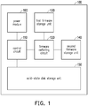
- FIG. 1 is a schematic block diagram of a solid-state disk according to an embodiment of the disclosure.
- a solid-state disk 100 includes a control circuit 110, a firmware switching circuit 120, a first firmware storage unit 130, a second firmware storage unit 140, a solid-state disk storage unit 150, and a power module 160.
- the control circuit 110 is coupled to the firmware switching circuit 120, the solid-state disk storage unit 150 and the power module 160.
- the firmware switching circuit 120 is further coupled to the first firmware storage unit 130 and the second firmware storage unit 140.
- the first firmware storage unit 130 is configured to store the first firmware.
- the second firmware storage unit 140 is configured to store the second firmware.
- the control circuit 110 is configured to read the first firmware storage unit 130 or the second firmware storage unit 140 according to whether the firmware switching circuit 120 is triggered so as to startup according to the first firmware or the second firmware.
- the second firmware storage unit 140 can be configured to store backup firmware.
- the control circuit 110 can update the first firmware stored in the first firmware storage unit 130.
- the control circuit 110 is started up after the firmware update of the first firmware storage unit 130 is completed, if the control circuit 110 reads the first firmware stored in the first firmware storage unit 130 to perform the startup operation and the operation fails, the firmware switching circuit 120 will be triggered. Therefore, when the control circuit 110 restarts, the control circuit 110 will read the second firmware stored in the second firmware storage unit 140 through the triggered firmware switching circuit 120 to restart.
- the solid-state disk 100 of the embodiment can effectively overcome the problem that the solid-state disk 100 cannot function when the control circuit 110 cannot perform the startup operation based on the firmware that fails to be updated when the solid-state disk 100 encounters firmware update failure.
- the disclosure is not limited to the above application examples.
- the first firmware stored in the first firmware storage unit 130 and the second firmware stored in the second firmware storage unit 140 can be respectively executed by the control circuit to achieve different access performance or different levels of energy saving.
- the control circuit 110 of the solid-state disk 100 can selectively trigger the firmware switching circuit 120 according to the following factors such as the operating performance of the central processing unit (CPU), the power supply status of the power module 160, or the ambient temperature, etc., so as to selectively read the first firmware stored in the first firmware storage unit 130 or the second firmware stored in the second firmware storage unit 140 to perform the startup operation according to the trigger result of the firmware switching circuit 120.
- the first firmware stored in the first firmware storage unit 130 and the second firmware stored in the second firmware storage unit 140 may be different firmware versions, and solid-state disk 100 can trigger the firmware switching circuit 120 through manual switching by the user, so that the control circuit 110 of the solid-state disk 100 can selectively read the first firmware stored in the first firmware storage unit 130 or the second firmware stored in the second firmware storage unit 140 to perform the startup operation.
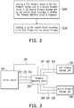
- FIG. 2 is a flowchart of a startup method according to an embodiment of the disclosure.
- the startup method of this embodiment can be at least adapted to the solid-state disk 100 in FIG. 1 .
- the control circuit 110 reads the first firmware stored in the first firmware storage unit 130 or the second firmware stored in the second firmware storage unit 140 according to whether the firmware switching circuit 120 is triggered.
- the control circuit 110 is started up according to the first firmware or the second firmware. Therefore, the startup method of this embodiment can enable the solid-state disk 100 to effectively perform the startup operation of the control circuit 110.
- sufficient teachings, suggestions, and implementation descriptions can be derived from the embodiment of FIG. 1 , and no further details are narrated herein.
- FIG. 3 is a schematic circuit diagram of a switching circuit according to an embodiment of the disclosure.
- the switching circuit of the solid-state disk of the disclosure can be as shown in FIG. 3 .
- the multiple pins of the control circuit 310 can be electrically connected to the firmware switching circuit 320 through lines 311 to 313, wherein the multiple pins can include chip selection (CS) pins, write protection (WP) pins, and hold pins.
- the firmware switching circuit 320 switches the above-mentioned multiple pins of the control circuit 310 respectively to be coupled to the first firmware storage unit 330 or the second firmware storage unit 340 through the lines 321 to 323 and the lines 324 to 326 respectively.
- an additional trace 301 can be electrically connected between the control circuit 310 and the firmware switching circuit 320 of this embodiment.
- the control circuit 310 can provide a trigger signal to the firmware switching circuit 320 through the trace 301 to trigger the firmware switching circuit 320.
- the control circuit 310 accesses the first firmware stored in the first firmware storage unit 330 through the firmware switching circuit 320. Moreover, after the firmware switching circuit 320 is triggered, the control circuit 310 accesses the second firmware stored in the second firmware storage unit 340 through the firmware switching circuit 320.
- the firmware switching circuit 320 receives the trigger signal from the control circuit 310 only through the trace 301.
- the firmware switching circuit 320 can also be connected to a trigger unit manually triggered by the user through another additional trace, so as to receive another trigger signal generated by the user's trigger to determine the object to be accessed by the control circuit 310.
- FIG. 4 is a flowchart of a startup method according to another embodiment of the disclosure.
- the startup method of this embodiment is at least adaptable for the solid-state disk 100 of FIG. 1 .
- the control circuit 110 performs a startup operation.
- the control circuit 110 determines whether the firmware switching circuit 120 is triggered. If not, the solid-state disk 100 executes step S430.
- the control circuit 110 reads the first firmware stored in the first firmware storage unit 130 through the firmware switching circuit 120.
- the control circuit 110 executes the first firmware to perform a startup operation.
- step S450 the control circuit 110 determines whether the startup operation is successful. If yes, the solid-state disk 100 executes step S470.
- the control circuit 110 ends the startup operation. However, if not, the solid-state disk 100 executes step S460.
- step S460 the control circuit 110 triggers the firmware switching circuit 120. Then, the control circuit 110 executes step S410 again to restart.
- step S440 the control circuit 110 reads the second firmware stored in the second firmware storage unit 140 through the firmware switching circuit 120. The control circuit 110 executes the second firmware to perform the startup operation again, and the control circuit 110 continues to execute step S450 and step S470. Therefore, the startup method of this embodiment can enable the solid-state disk 100 to effectively perform the startup operation of the control circuit 110.
- step S440 the control circuit 110 reads the second firmware stored in the second firmware storage unit 140 through the firmware switching circuit 120.
- the control circuit 110 executes the second firmware to perform the startup operation again, and the control circuit 110 continues to execute step S450 and step S470. Therefore, the startup method of this embodiment can enable the solid-state disk 100 to effectively perform the startup operation of the control circuit 110.
- sufficient teachings, suggestions, and implementation descriptions can be derived from the embodiment of FIG. 1 , and no further details are narrated herein.
- two firmwares can be stored in two firmware storage units, and a firmware switching circuit is arranged between the control circuit and the two firmware storage units, so as to determine that the control circuit accesses the firmware of the solid-state disk from one of the two firmware storage units according to whether the firmware switching circuit is triggered.
- the trigger mode of the firmware switching circuit can be automatic or manual. Accordingly, the solid-state disk and the startup method of the disclosure can provide the function of being able to read the effective firmware of the solid-state disk for startup operation, or may provide the function of being able to selectively read the specific firmware for special startup operation.
Landscapes
- Engineering & Computer Science (AREA)
- Theoretical Computer Science (AREA)
- Software Systems (AREA)
- Physics & Mathematics (AREA)
- General Engineering & Computer Science (AREA)
- General Physics & Mathematics (AREA)
- Quality & Reliability (AREA)
- Computing Systems (AREA)
- Computer Security & Cryptography (AREA)
- Computer Hardware Design (AREA)
- Mathematical Physics (AREA)
- Stored Programmes (AREA)
- Memory System (AREA)
Abstract
Description
- The disclosure relates to a disk startup technology, and particularly relates to a solid-state disk and a startup method.
- For a general solid-state disk, the firmware of the solid-state disk may be updated, for example, to the firmware data of a newer firmware version provided by the disk manufacturer. However, when the firmware update fails, the normal solid-state disk will not be able to perform normal startup operations because it cannot read valid firmware data, and the user may have to send the solid-state disk to the manufacturer to reprogram the firmware storage unit so that the solid-state disk can perform operation again. In view of this, when the solid-state disk fails to update the firmware and the solid-state disk cannot perform startup operation based on the firmware with update failure, to effectively overcome the problem, the disclosure provides some embodiments of solutions as follows.
- The disclosure provides a solid-state disk and a startup method, which can effectively perform the startup operation of the control circuit of the solid-state disk.
- In the disclosure, the solid-state disk includes a control circuit, a firmware switching circuit, a first firmware storage unit, and a second firmware storage unit. The firmware switching circuit is coupled to the control circuit. The first firmware storage unit is coupled to the firmware switching circuit and stores a first firmware. The second firmware storage unit is coupled to the firmware switching circuit and stores a second firmware. The control circuit reads the first firmware storage unit or the second firmware storage unit according to whether the firmware switching circuit is triggered so as to startup according to the first firmware or the second firmware.
- The startup method of the disclosure is adaptable for a solid-state disk. The solid-state disk includes a control circuit, a firmware switching circuit, a first firmware storage unit, and a second firmware storage unit. The startup method includes: reading the first firmware stored in the first firmware storage unit or the second firmware stored in the second firmware storage unit by the control circuit according to whether the firmware switching circuit is triggered; starting up by the control circuit according to the first firmware or the second firmware.
- Based on the above, through the solid-state disk and the startup method of the disclosure, two firmwares can be stored in two firmware storage units for the control circuit to read selectively, so that the solid-state disk can be started up.
- In order to make the above-mentioned features and advantages of the disclosure more comprehensible, the embodiments are specifically described below in detail with reference to the accompanying drawings.
-
-
FIG. 1 is a schematic block diagram of a solid-state disk according to an embodiment of the disclosure. -
FIG. 2 is a flowchart of a startup method according to an embodiment of the disclosure. -
FIG. 3 is a schematic circuit diagram of a switching circuit according to an embodiment of the disclosure. -
FIG. 4 is a flowchart of a startup method according to another embodiment of the disclosure. - In order to make the content of this disclosure to be more comprehensible, the following embodiments are specifically cited as examples based on which this disclosure can indeed be implemented. In addition, wherever possible, elements/components/steps with the same reference numbers in the drawings and embodiments represent the same or similar components.
-
FIG. 1 is a schematic block diagram of a solid-state disk according to an embodiment of the disclosure. Referring toFIG. 1 , a solid-state disk 100 includes acontrol circuit 110, afirmware switching circuit 120, a firstfirmware storage unit 130, a secondfirmware storage unit 140, a solid-statedisk storage unit 150, and apower module 160. Thecontrol circuit 110 is coupled to thefirmware switching circuit 120, the solid-statedisk storage unit 150 and thepower module 160. Thefirmware switching circuit 120 is further coupled to the firstfirmware storage unit 130 and the secondfirmware storage unit 140. In this embodiment, the firstfirmware storage unit 130 is configured to store the first firmware. The secondfirmware storage unit 140 is configured to store the second firmware. Thecontrol circuit 110 is configured to read the firstfirmware storage unit 130 or the secondfirmware storage unit 140 according to whether thefirmware switching circuit 120 is triggered so as to startup according to the first firmware or the second firmware. - For example, the second
firmware storage unit 140 can be configured to store backup firmware. When the solid-state disk 100 is updating the firmware, thecontrol circuit 110 can update the first firmware stored in the firstfirmware storage unit 130. However, when thecontrol circuit 110 is started up after the firmware update of the firstfirmware storage unit 130 is completed, if thecontrol circuit 110 reads the first firmware stored in the firstfirmware storage unit 130 to perform the startup operation and the operation fails, thefirmware switching circuit 120 will be triggered. Therefore, when thecontrol circuit 110 restarts, thecontrol circuit 110 will read the second firmware stored in the secondfirmware storage unit 140 through the triggeredfirmware switching circuit 120 to restart. In other words, the solid-state disk 100 of the embodiment can effectively overcome the problem that the solid-state disk 100 cannot function when thecontrol circuit 110 cannot perform the startup operation based on the firmware that fails to be updated when the solid-state disk 100 encounters firmware update failure. - However, the disclosure is not limited to the above application examples. In other application examples, the first firmware stored in the first
firmware storage unit 130 and the second firmware stored in the secondfirmware storage unit 140 can be respectively executed by the control circuit to achieve different access performance or different levels of energy saving. Thecontrol circuit 110 of the solid-state disk 100 can selectively trigger thefirmware switching circuit 120 according to the following factors such as the operating performance of the central processing unit (CPU), the power supply status of thepower module 160, or the ambient temperature, etc., so as to selectively read the first firmware stored in the firstfirmware storage unit 130 or the second firmware stored in the secondfirmware storage unit 140 to perform the startup operation according to the trigger result of thefirmware switching circuit 120. Or, in another application example, the first firmware stored in the firstfirmware storage unit 130 and the second firmware stored in the secondfirmware storage unit 140 may be different firmware versions, and solid-state disk 100 can trigger thefirmware switching circuit 120 through manual switching by the user, so that thecontrol circuit 110 of the solid-state disk 100 can selectively read the first firmware stored in the firstfirmware storage unit 130 or the second firmware stored in the secondfirmware storage unit 140 to perform the startup operation. -
FIG. 2 is a flowchart of a startup method according to an embodiment of the disclosure. Referring toFIG. 1 andFIG. 2 , the startup method of this embodiment can be at least adapted to the solid-state disk 100 inFIG. 1 . In step S210, thecontrol circuit 110 reads the first firmware stored in the firstfirmware storage unit 130 or the second firmware stored in the secondfirmware storage unit 140 according to whether thefirmware switching circuit 120 is triggered. In step S220, thecontrol circuit 110 is started up according to the first firmware or the second firmware. Therefore, the startup method of this embodiment can enable the solid-state disk 100 to effectively perform the startup operation of thecontrol circuit 110. In addition, regarding other device features, implementation examples, and technical details of the solid-state disk 100 of this embodiment, sufficient teachings, suggestions, and implementation descriptions can be derived from the embodiment ofFIG. 1 , and no further details are narrated herein. -
FIG. 3 is a schematic circuit diagram of a switching circuit according to an embodiment of the disclosure. Referring toFIG. 3 , the switching circuit of the solid-state disk of the disclosure can be as shown inFIG. 3 . The multiple pins of thecontrol circuit 310 can be electrically connected to thefirmware switching circuit 320 throughlines 311 to 313, wherein the multiple pins can include chip selection (CS) pins, write protection (WP) pins, and hold pins. Thefirmware switching circuit 320 switches the above-mentioned multiple pins of thecontrol circuit 310 respectively to be coupled to the firstfirmware storage unit 330 or the secondfirmware storage unit 340 through thelines 321 to 323 and thelines 324 to 326 respectively. It is worth noting that anadditional trace 301 can be electrically connected between thecontrol circuit 310 and thefirmware switching circuit 320 of this embodiment. When thecontrol circuit 310 encounters the situation described in the above example or other situations, thecontrol circuit 310 can provide a trigger signal to thefirmware switching circuit 320 through thetrace 301 to trigger thefirmware switching circuit 320. - In other words, before the
firmware switching circuit 320 is triggered, thecontrol circuit 310 accesses the first firmware stored in the firstfirmware storage unit 330 through thefirmware switching circuit 320. Moreover, after thefirmware switching circuit 320 is triggered, thecontrol circuit 310 accesses the second firmware stored in the secondfirmware storage unit 340 through thefirmware switching circuit 320. However, it is not limited that thefirmware switching circuit 320 receives the trigger signal from thecontrol circuit 310 only through thetrace 301. In another embodiment, thefirmware switching circuit 320 can also be connected to a trigger unit manually triggered by the user through another additional trace, so as to receive another trigger signal generated by the user's trigger to determine the object to be accessed by thecontrol circuit 310. -
FIG. 4 is a flowchart of a startup method according to another embodiment of the disclosure. Referring toFIG. 1 andFIG. 4 , the startup method of this embodiment is at least adaptable for the solid-state disk 100 ofFIG. 1 . In step S410, thecontrol circuit 110 performs a startup operation. Thecontrol circuit 110 determines whether thefirmware switching circuit 120 is triggered. If not, the solid-state disk 100 executes step S430. In step S430, thecontrol circuit 110 reads the first firmware stored in the firstfirmware storage unit 130 through thefirmware switching circuit 120. Thecontrol circuit 110 executes the first firmware to perform a startup operation. In step S450, thecontrol circuit 110 determines whether the startup operation is successful. If yes, the solid-state disk 100 executes step S470. In step S470, thecontrol circuit 110 ends the startup operation. However, if not, the solid-state disk 100 executes step S460. - In step S460, the
control circuit 110 triggers thefirmware switching circuit 120. Then, thecontrol circuit 110 executes step S410 again to restart. When thecontrol circuit 110 performs step S420 again, because thecontrol circuit 110 determines that thefirmware switching circuit 120 is triggered, thecontrol circuit 110 executes step S440. In step S440, thecontrol circuit 110 reads the second firmware stored in the secondfirmware storage unit 140 through thefirmware switching circuit 120. Thecontrol circuit 110 executes the second firmware to perform the startup operation again, and thecontrol circuit 110 continues to execute step S450 and step S470. Therefore, the startup method of this embodiment can enable the solid-state disk 100 to effectively perform the startup operation of thecontrol circuit 110. In addition, regarding other device features, implementation examples, and technical details of the solid-state disk 100 of this embodiment, sufficient teachings, suggestions, and implementation descriptions can be derived from the embodiment ofFIG. 1 , and no further details are narrated herein. - In summary, through the solid-state disk and the startup method of the disclosure, two firmwares can be stored in two firmware storage units, and a firmware switching circuit is arranged between the control circuit and the two firmware storage units, so as to determine that the control circuit accesses the firmware of the solid-state disk from one of the two firmware storage units according to whether the firmware switching circuit is triggered. Moreover, the trigger mode of the firmware switching circuit can be automatic or manual. Accordingly, the solid-state disk and the startup method of the disclosure can provide the function of being able to read the effective firmware of the solid-state disk for startup operation, or may provide the function of being able to selectively read the specific firmware for special startup operation.
Claims (14)
- A solid-state disk (100), comprising:a control circuit (110, 310);a firmware switching circuit (120, 320), coupled to the control circuit (110, 310);a first firmware storage unit (130, 330), coupled to the firmware switching circuit (120, 320), and configured to store a first firmware; anda second firmware storage unit (140, 340), coupled to the firmware switching circuit (120, 320), and configured to store a second firmware,wherein the control circuit (110, 310) is configured to read the first firmware storage unit (130, 330) or the second firmware storage unit (140, 340) according to whether the firmware switching circuit (120, 320) is triggered so as to startup according to the first firmware or the second firmware.
- The solid-state disk (100) according to claim 1, wherein the control circuit (110, 310) is preset to read the first firmware of the first firmware storage unit (130, 330) to startup according to the first firmware, and when the control circuit (110, 310) fails to startup according to the first firmware, the firmware switching circuit (120, 320) is triggered to switch the control circuit (110, 310) to read the second firmware of the second firmware storage unit (140, 340), and the control circuit (110, 310) starts up again according to the second firmware.
- The solid-state disk (100) according to claim 1, wherein when the control circuit (110, 310) fails to startup, the control circuit (110, 310) outputs a trigger signal to the firmware switching circuit (120, 320) through a trace (301) coupled to the firmware switching circuit (120, 320) to trigger the firmware switching circuit (120, 320) to switch the control circuit (110, 310) to read the first firmware storage unit (130, 330) or the second firmware storage unit (140, 340).
- The solid-state disk (100) according to claim 1, wherein the firmware switching circuit (120, 320) receives a trigger signal externally to trigger the firmware switching circuit (120, 320) to switch the control circuit (110, 310) to read the first firmware storage unit (130, 330) or the second firmware storage unit (140, 340).
- The solid-state disk (100) according to claim 1, wherein the first firmware and the second firmware are respectively executed by the control circuit (110, 310) to achieve different access performance or different levels of energy saving.
- The solid-state disk (100) according to claim 1, wherein the first firmware and the second firmware are different firmware versions.
- The solid-state disk (100) according to claim 1, wherein the firmware switching circuit (120, 320) is configured to switch a plurality of pins of the control circuit (110, 310) to be coupled to the first firmware storage unit (130, 330) or the second firmware storage unit (140, 340), wherein the plurality of pins comprises a chip selection pin, a write protection pin and a hold pin.
- A startup method, adaptable for a solid-state disk (100), wherein the solid-state disk (100) comprises a control circuit (110, 310), a firmware switching circuit (120, 320), a first firmware storage unit (130, 330) and a second firmware storage unit (140, 340), and the startup method comprising:reading a first firmware stored in the first firmware storage unit (130, 330) or a second firmware stored in the second firmware storage unit (140, 340) by the control circuit (110, 310) according to whether the firmware switching circuit (120, 320) is triggered; andstarting up by the control circuit (110, 310) according to the first firmware or the second firmware.
- The startup method according to claim 8, wherein the step of reading the first firmware stored in the first firmware storage unit (130, 330) or the second firmware stored in the second firmware storage unit (140, 340) by the control circuit (110, 310) according to whether the firmware switching circuit (120, 320) is triggered comprises:reading the first firmware of the first firmware storage unit (130, 330) by the preset control circuit (110, 310) to startup the solid-state disk (100) according to the first firmware; andwhen the control circuit (110, 310) fails to startup according to the first firmware, the firmware switching circuit (120, 320) is triggered to switch the control circuit (110, 310) to read the second firmware of the second firmware storage unit (140, 340), and to startup again according to the second firmware.
- The startup method according to claim 9, wherein when the control circuit (110, 310) fails to startup the solid-state disk (100) according to the first firmware, the step of triggering the firmware switching circuit (120, 320) to switch the control circuit (110, 310) to read the second firmware of the second firmware storage unit (140, 340), and to startup again according to the second firmware comprises:
outputting, by the control circuit (110, 310), a trigger signal to the firmware switching circuit (120, 320) through a trace (301) coupled to the firmware switching circuit (120, 320) to trigger the firmware switching circuit (120, 320) to switch the control circuit (110, 310) to read the second firmware storage unit (140, 340). - The startup method according to claim 8, wherein the step of reading the first firmware stored in the first firmware storage unit (130, 330) or the second firmware stored in the second firmware storage unit (140, 340) by the control circuit (110, 310) according to whether the firmware switching circuit (120, 320) is triggered comprises:
receiving, by the firmware switching circuit (120, 320), a trigger signal externally to trigger the firmware switching circuit (120, 320) to switch the control circuit (110, 310) to read the first firmware storage unit (130, 330) or the second firmware storage unit (140, 340). - The startup method according to claim 8, wherein the first firmware and the second firmware are respectively executed by the control circuit (110, 310) to achieve different access performance or different levels of energy saving.
- The startup method according to claim 8, wherein the first firmware and the second firmware are different firmware versions.
- The startup method according to claim 8, wherein the firmware switching circuit (120, 320) is configured to switch a plurality of pins of the control circuit (110, 310) to be coupled to the first firmware storage unit (130, 330) or the second firmware storage unit (140, 340), wherein the plurality of pins comprises a chip selection pin, a write protection pin and a hold pin.
Applications Claiming Priority (1)
| Application Number | Priority Date | Filing Date | Title |
|---|---|---|---|
| TW109110752A TWI722852B (en) | 2020-03-30 | 2020-03-30 | Solid-state disk and startup method |
Publications (2)
| Publication Number | Publication Date |
|---|---|
| EP3889769A1 true EP3889769A1 (en) | 2021-10-06 |
| EP3889769B1 EP3889769B1 (en) | 2024-08-28 |
Family
ID=74105873
Family Applications (1)
| Application Number | Title | Priority Date | Filing Date |
|---|---|---|---|
| EP21150464.2A Active EP3889769B1 (en) | 2020-03-30 | 2021-01-07 | Solid-state disk and startup method |
Country Status (5)
| Country | Link |
|---|---|
| US (1) | US11226863B2 (en) |
| EP (1) | EP3889769B1 (en) |
| JP (1) | JP7279095B2 (en) |
| KR (1) | KR20210122661A (en) |
| TW (1) | TWI722852B (en) |
Families Citing this family (2)
| Publication number | Priority date | Publication date | Assignee | Title |
|---|---|---|---|---|
| WO2024243844A1 (en) * | 2023-05-31 | 2024-12-05 | 威刚科技股份有限公司 | Electronic device, solid-state drive device, and artificial satellite |
| US20250165347A1 (en) * | 2023-11-20 | 2025-05-22 | Micron Technology, Inc. | Memory sub-system recovery in response to host hardware recovery signal |
Citations (1)
| Publication number | Priority date | Publication date | Assignee | Title |
|---|---|---|---|---|
| US20190073268A1 (en) * | 2017-09-06 | 2019-03-07 | Western Digital Technologies, Inc. | System and method for switching firmware |
Family Cites Families (15)
| Publication number | Priority date | Publication date | Assignee | Title |
|---|---|---|---|---|
| US6301344B1 (en) * | 1997-11-05 | 2001-10-09 | Protel, Inc. | Intelligent public telephone system and method |
| JP2004199277A (en) * | 2002-12-17 | 2004-07-15 | Fujitsu Ltd | BIOS redundancy management method, data processing device, and storage system |
| US7340595B2 (en) * | 2005-01-07 | 2008-03-04 | International Business Machines Corporation | Multiplex execution-path system |
| US20070136502A1 (en) * | 2005-12-14 | 2007-06-14 | Mediatek Inc. | SPI device |
| JP2008299709A (en) | 2007-06-01 | 2008-12-11 | Nec Corp | Firmware updating system, network connection apparatus, firmware updating method, and program |
| JP2010170197A (en) * | 2009-01-20 | 2010-08-05 | Toshiba Storage Device Corp | Firmware management program, storage device, and firmware management method |
| US8046631B2 (en) * | 2009-04-29 | 2011-10-25 | Lsi Corporation | Firmware recovery in a raid controller by using a dual firmware configuration |
| JP5431111B2 (en) * | 2009-10-22 | 2014-03-05 | 株式会社日立製作所 | Information processing apparatus and system setting method |
| US8412876B2 (en) * | 2010-06-30 | 2013-04-02 | Felicity Taiwan Corporation | Storage device with multiple storage units and control method thereof |
| JP2015099408A (en) | 2012-03-14 | 2015-05-28 | オムロン株式会社 | Bios booting device and mother board |
| US9785596B2 (en) * | 2013-04-23 | 2017-10-10 | Hewlett-Packard Development Company, L.P. | Redundant system boot code in a secondary non-volatile memory |
| CN104536848B (en) * | 2014-12-22 | 2018-05-08 | 小米科技有限责任公司 | Firmware restoration method, apparatus and terminal |
| US9934151B2 (en) * | 2016-06-28 | 2018-04-03 | Dell Products, Lp | System and method for dynamic optimization for burst and sustained performance in solid state drives |
| JP2018014050A (en) * | 2016-07-22 | 2018-01-25 | 東芝メモリ株式会社 | Memory system |
| US10146527B2 (en) * | 2016-10-12 | 2018-12-04 | Samsung Electronics Co., Ltd. | Method and apparatus for using BMC as proxy for NVME over fabrics device firmware upgrade |
-
2020
- 2020-03-30 TW TW109110752A patent/TWI722852B/en active
- 2020-12-13 US US17/120,247 patent/US11226863B2/en active Active
- 2020-12-29 KR KR1020200186493A patent/KR20210122661A/en not_active Ceased
-
2021
- 2021-01-07 EP EP21150464.2A patent/EP3889769B1/en active Active
- 2021-02-25 JP JP2021028227A patent/JP7279095B2/en active Active
Patent Citations (1)
| Publication number | Priority date | Publication date | Assignee | Title |
|---|---|---|---|---|
| US20190073268A1 (en) * | 2017-09-06 | 2019-03-07 | Western Digital Technologies, Inc. | System and method for switching firmware |
Also Published As
| Publication number | Publication date |
|---|---|
| TW202137225A (en) | 2021-10-01 |
| US11226863B2 (en) | 2022-01-18 |
| JP7279095B2 (en) | 2023-05-22 |
| US20210303402A1 (en) | 2021-09-30 |
| JP2021163472A (en) | 2021-10-11 |
| EP3889769B1 (en) | 2024-08-28 |
| KR20210122661A (en) | 2021-10-12 |
| TWI722852B (en) | 2021-03-21 |
Similar Documents
| Publication | Publication Date | Title |
|---|---|---|
| EP2506114B1 (en) | Method and device for intelligent terminal reset | |
| US8468389B2 (en) | Firmware recovery system and method of baseboard management controller of computing device | |
| TWI382346B (en) | Computer system with dual bios protection mechanism and control method of the same | |
| US20110093741A1 (en) | Method for recovering bios and computer system thereof | |
| US20230060908A1 (en) | Computer system and method for booting up the computer system | |
| US11314665B2 (en) | Information processing system, information processing device, BIOS updating method for information processing device, and BIOS updating program for information processing device | |
| CN101017441A (en) | Electric device, start method of electric and update method of BIOS | |
| US8930931B2 (en) | Information processing apparatus using updated firmware and system setting method | |
| CN102446104A (en) | Method for starting up computer system | |
| US11226863B2 (en) | Solid-state disk and startup method | |
| CN114528557A (en) | Self-adaptive starting method of embedded SOC chip | |
| CN115904512A (en) | Method of Realizing High Reliable Startup of Embedded System Based on CPLD | |
| JP5665923B2 (en) | Electronic device capable of updating basic input / output system and update method | |
| CN106325903A (en) | A start processing method and device | |
| US9652259B2 (en) | Apparatus and method for managing register information in a processing system | |
| CN113672306B (en) | Method, device, system and medium for recovery from abnormal self-checking of server components | |
| CN101158907A (en) | Bootloader online upgrade method | |
| CN111666094B (en) | Real-time firmware upgrading system and method | |
| US20080301427A1 (en) | Basic input/output system memory simulation module | |
| KR100605031B1 (en) | Fault recovery and upgrade method of embedded system using USB memory device | |
| CN101739315A (en) | System and method for automatically starting backup firmware | |
| CN113467796B (en) | Solid state disk and starting method | |
| US12332712B2 (en) | Method of updating power firmware and power supply | |
| CN113467848A (en) | Multi-system startup method, device, storage medium, and program product | |
| CN111221701A (en) | Chip and circuit logic reconfiguration system thereof |
Legal Events
| Date | Code | Title | Description |
|---|---|---|---|
| PUAI | Public reference made under article 153(3) epc to a published international application that has entered the european phase |
Free format text: ORIGINAL CODE: 0009012 |
|
| STAA | Information on the status of an ep patent application or granted ep patent |
Free format text: STATUS: THE APPLICATION HAS BEEN PUBLISHED |
|
| AK | Designated contracting states |
Kind code of ref document: A1 Designated state(s): AL AT BE BG CH CY CZ DE DK EE ES FI FR GB GR HR HU IE IS IT LI LT LU LV MC MK MT NL NO PL PT RO RS SE SI SK SM TR |
|
| STAA | Information on the status of an ep patent application or granted ep patent |
Free format text: STATUS: REQUEST FOR EXAMINATION WAS MADE |
|
| 17P | Request for examination filed |
Effective date: 20211201 |
|
| RBV | Designated contracting states (corrected) |
Designated state(s): AL AT BE BG CH CY CZ DE DK EE ES FI FR GB GR HR HU IE IS IT LI LT LU LV MC MK MT NL NO PL PT RO RS SE SI SK SM TR |
|
| STAA | Information on the status of an ep patent application or granted ep patent |
Free format text: STATUS: EXAMINATION IS IN PROGRESS |
|
| 17Q | First examination report despatched |
Effective date: 20230829 |
|
| GRAP | Despatch of communication of intention to grant a patent |
Free format text: ORIGINAL CODE: EPIDOSNIGR1 |
|
| STAA | Information on the status of an ep patent application or granted ep patent |
Free format text: STATUS: GRANT OF PATENT IS INTENDED |
|
| INTG | Intention to grant announced |
Effective date: 20240429 |
|
| GRAS | Grant fee paid |
Free format text: ORIGINAL CODE: EPIDOSNIGR3 |
|
| GRAA | (expected) grant |
Free format text: ORIGINAL CODE: 0009210 |
|
| STAA | Information on the status of an ep patent application or granted ep patent |
Free format text: STATUS: THE PATENT HAS BEEN GRANTED |
|
| AK | Designated contracting states |
Kind code of ref document: B1 Designated state(s): AL AT BE BG CH CY CZ DE DK EE ES FI FR GB GR HR HU IE IS IT LI LT LU LV MC MK MT NL NO PL PT RO RS SE SI SK SM TR |
|
| REG | Reference to a national code |
Ref country code: CH Ref legal event code: EP |
|
| REG | Reference to a national code |
Ref country code: DE Ref legal event code: R096 Ref document number: 602021017714 Country of ref document: DE |
|
| REG | Reference to a national code |
Ref country code: IE Ref legal event code: FG4D |
|
| REG | Reference to a national code |
Ref country code: LT Ref legal event code: MG9D |
|
| PG25 | Lapsed in a contracting state [announced via postgrant information from national office to epo] |
Ref country code: NO Free format text: LAPSE BECAUSE OF FAILURE TO SUBMIT A TRANSLATION OF THE DESCRIPTION OR TO PAY THE FEE WITHIN THE PRESCRIBED TIME-LIMIT Effective date: 20241128 |
|
| REG | Reference to a national code |
Ref country code: AT Ref legal event code: MK05 Ref document number: 1718704 Country of ref document: AT Kind code of ref document: T Effective date: 20240828 |
|
| PG25 | Lapsed in a contracting state [announced via postgrant information from national office to epo] |
Ref country code: NL Free format text: LAPSE BECAUSE OF FAILURE TO SUBMIT A TRANSLATION OF THE DESCRIPTION OR TO PAY THE FEE WITHIN THE PRESCRIBED TIME-LIMIT Effective date: 20240828 Ref country code: GR Free format text: LAPSE BECAUSE OF FAILURE TO SUBMIT A TRANSLATION OF THE DESCRIPTION OR TO PAY THE FEE WITHIN THE PRESCRIBED TIME-LIMIT Effective date: 20241129 Ref country code: PL Free format text: LAPSE BECAUSE OF FAILURE TO SUBMIT A TRANSLATION OF THE DESCRIPTION OR TO PAY THE FEE WITHIN THE PRESCRIBED TIME-LIMIT Effective date: 20240828 Ref country code: FI Free format text: LAPSE BECAUSE OF FAILURE TO SUBMIT A TRANSLATION OF THE DESCRIPTION OR TO PAY THE FEE WITHIN THE PRESCRIBED TIME-LIMIT Effective date: 20240828 Ref country code: PT Free format text: LAPSE BECAUSE OF FAILURE TO SUBMIT A TRANSLATION OF THE DESCRIPTION OR TO PAY THE FEE WITHIN THE PRESCRIBED TIME-LIMIT Effective date: 20241230 |
|
| PG25 | Lapsed in a contracting state [announced via postgrant information from national office to epo] |
Ref country code: BG Free format text: LAPSE BECAUSE OF FAILURE TO SUBMIT A TRANSLATION OF THE DESCRIPTION OR TO PAY THE FEE WITHIN THE PRESCRIBED TIME-LIMIT Effective date: 20240828 |
|
| PG25 | Lapsed in a contracting state [announced via postgrant information from national office to epo] |
Ref country code: LV Free format text: LAPSE BECAUSE OF FAILURE TO SUBMIT A TRANSLATION OF THE DESCRIPTION OR TO PAY THE FEE WITHIN THE PRESCRIBED TIME-LIMIT Effective date: 20240828 |
|
| REG | Reference to a national code |
Ref country code: NL Ref legal event code: MP Effective date: 20240828 |
|
| PG25 | Lapsed in a contracting state [announced via postgrant information from national office to epo] |
Ref country code: AT Free format text: LAPSE BECAUSE OF FAILURE TO SUBMIT A TRANSLATION OF THE DESCRIPTION OR TO PAY THE FEE WITHIN THE PRESCRIBED TIME-LIMIT Effective date: 20240828 Ref country code: IS Free format text: LAPSE BECAUSE OF FAILURE TO SUBMIT A TRANSLATION OF THE DESCRIPTION OR TO PAY THE FEE WITHIN THE PRESCRIBED TIME-LIMIT Effective date: 20241228 |
|
| PG25 | Lapsed in a contracting state [announced via postgrant information from national office to epo] |
Ref country code: HR Free format text: LAPSE BECAUSE OF FAILURE TO SUBMIT A TRANSLATION OF THE DESCRIPTION OR TO PAY THE FEE WITHIN THE PRESCRIBED TIME-LIMIT Effective date: 20240828 |
|
| PG25 | Lapsed in a contracting state [announced via postgrant information from national office to epo] |
Ref country code: RS Free format text: LAPSE BECAUSE OF FAILURE TO SUBMIT A TRANSLATION OF THE DESCRIPTION OR TO PAY THE FEE WITHIN THE PRESCRIBED TIME-LIMIT Effective date: 20241128 Ref country code: ES Free format text: LAPSE BECAUSE OF FAILURE TO SUBMIT A TRANSLATION OF THE DESCRIPTION OR TO PAY THE FEE WITHIN THE PRESCRIBED TIME-LIMIT Effective date: 20240828 |
|
| PG25 | Lapsed in a contracting state [announced via postgrant information from national office to epo] |
Ref country code: RS Free format text: LAPSE BECAUSE OF FAILURE TO SUBMIT A TRANSLATION OF THE DESCRIPTION OR TO PAY THE FEE WITHIN THE PRESCRIBED TIME-LIMIT Effective date: 20241128 Ref country code: PT Free format text: LAPSE BECAUSE OF FAILURE TO SUBMIT A TRANSLATION OF THE DESCRIPTION OR TO PAY THE FEE WITHIN THE PRESCRIBED TIME-LIMIT Effective date: 20241230 Ref country code: PL Free format text: LAPSE BECAUSE OF FAILURE TO SUBMIT A TRANSLATION OF THE DESCRIPTION OR TO PAY THE FEE WITHIN THE PRESCRIBED TIME-LIMIT Effective date: 20240828 Ref country code: NO Free format text: LAPSE BECAUSE OF FAILURE TO SUBMIT A TRANSLATION OF THE DESCRIPTION OR TO PAY THE FEE WITHIN THE PRESCRIBED TIME-LIMIT Effective date: 20241128 Ref country code: NL Free format text: LAPSE BECAUSE OF FAILURE TO SUBMIT A TRANSLATION OF THE DESCRIPTION OR TO PAY THE FEE WITHIN THE PRESCRIBED TIME-LIMIT Effective date: 20240828 Ref country code: LV Free format text: LAPSE BECAUSE OF FAILURE TO SUBMIT A TRANSLATION OF THE DESCRIPTION OR TO PAY THE FEE WITHIN THE PRESCRIBED TIME-LIMIT Effective date: 20240828 Ref country code: IS Free format text: LAPSE BECAUSE OF FAILURE TO SUBMIT A TRANSLATION OF THE DESCRIPTION OR TO PAY THE FEE WITHIN THE PRESCRIBED TIME-LIMIT Effective date: 20241228 Ref country code: HR Free format text: LAPSE BECAUSE OF FAILURE TO SUBMIT A TRANSLATION OF THE DESCRIPTION OR TO PAY THE FEE WITHIN THE PRESCRIBED TIME-LIMIT Effective date: 20240828 Ref country code: GR Free format text: LAPSE BECAUSE OF FAILURE TO SUBMIT A TRANSLATION OF THE DESCRIPTION OR TO PAY THE FEE WITHIN THE PRESCRIBED TIME-LIMIT Effective date: 20241129 Ref country code: FI Free format text: LAPSE BECAUSE OF FAILURE TO SUBMIT A TRANSLATION OF THE DESCRIPTION OR TO PAY THE FEE WITHIN THE PRESCRIBED TIME-LIMIT Effective date: 20240828 Ref country code: ES Free format text: LAPSE BECAUSE OF FAILURE TO SUBMIT A TRANSLATION OF THE DESCRIPTION OR TO PAY THE FEE WITHIN THE PRESCRIBED TIME-LIMIT Effective date: 20240828 Ref country code: BG Free format text: LAPSE BECAUSE OF FAILURE TO SUBMIT A TRANSLATION OF THE DESCRIPTION OR TO PAY THE FEE WITHIN THE PRESCRIBED TIME-LIMIT Effective date: 20240828 Ref country code: AT Free format text: LAPSE BECAUSE OF FAILURE TO SUBMIT A TRANSLATION OF THE DESCRIPTION OR TO PAY THE FEE WITHIN THE PRESCRIBED TIME-LIMIT Effective date: 20240828 |
|
| PG25 | Lapsed in a contracting state [announced via postgrant information from national office to epo] |
Ref country code: RO Free format text: LAPSE BECAUSE OF FAILURE TO SUBMIT A TRANSLATION OF THE DESCRIPTION OR TO PAY THE FEE WITHIN THE PRESCRIBED TIME-LIMIT Effective date: 20240828 Ref country code: SM Free format text: LAPSE BECAUSE OF FAILURE TO SUBMIT A TRANSLATION OF THE DESCRIPTION OR TO PAY THE FEE WITHIN THE PRESCRIBED TIME-LIMIT Effective date: 20240828 Ref country code: DK Free format text: LAPSE BECAUSE OF FAILURE TO SUBMIT A TRANSLATION OF THE DESCRIPTION OR TO PAY THE FEE WITHIN THE PRESCRIBED TIME-LIMIT Effective date: 20240828 |
|
| PG25 | Lapsed in a contracting state [announced via postgrant information from national office to epo] |
Ref country code: EE Free format text: LAPSE BECAUSE OF FAILURE TO SUBMIT A TRANSLATION OF THE DESCRIPTION OR TO PAY THE FEE WITHIN THE PRESCRIBED TIME-LIMIT Effective date: 20240828 |
|
| PG25 | Lapsed in a contracting state [announced via postgrant information from national office to epo] |
Ref country code: CZ Free format text: LAPSE BECAUSE OF FAILURE TO SUBMIT A TRANSLATION OF THE DESCRIPTION OR TO PAY THE FEE WITHIN THE PRESCRIBED TIME-LIMIT Effective date: 20240828 |
|
| PG25 | Lapsed in a contracting state [announced via postgrant information from national office to epo] |
Ref country code: SK Free format text: LAPSE BECAUSE OF FAILURE TO SUBMIT A TRANSLATION OF THE DESCRIPTION OR TO PAY THE FEE WITHIN THE PRESCRIBED TIME-LIMIT Effective date: 20240828 Ref country code: IT Free format text: LAPSE BECAUSE OF FAILURE TO SUBMIT A TRANSLATION OF THE DESCRIPTION OR TO PAY THE FEE WITHIN THE PRESCRIBED TIME-LIMIT Effective date: 20240828 |
|
| REG | Reference to a national code |
Ref country code: DE Ref legal event code: R097 Ref document number: 602021017714 Country of ref document: DE |
|
| PLBE | No opposition filed within time limit |
Free format text: ORIGINAL CODE: 0009261 |
|
| STAA | Information on the status of an ep patent application or granted ep patent |
Free format text: STATUS: NO OPPOSITION FILED WITHIN TIME LIMIT |
|
| 26N | No opposition filed |
Effective date: 20250530 |
|
| REG | Reference to a national code |
Ref country code: CH Ref legal event code: PL |
|
| PG25 | Lapsed in a contracting state [announced via postgrant information from national office to epo] |
Ref country code: SE Free format text: LAPSE BECAUSE OF FAILURE TO SUBMIT A TRANSLATION OF THE DESCRIPTION OR TO PAY THE FEE WITHIN THE PRESCRIBED TIME-LIMIT Effective date: 20240828 |
|
| PG25 | Lapsed in a contracting state [announced via postgrant information from national office to epo] |
Ref country code: LU Free format text: LAPSE BECAUSE OF NON-PAYMENT OF DUE FEES Effective date: 20250107 Ref country code: MC Free format text: LAPSE BECAUSE OF FAILURE TO SUBMIT A TRANSLATION OF THE DESCRIPTION OR TO PAY THE FEE WITHIN THE PRESCRIBED TIME-LIMIT Effective date: 20240828 |
|
| PG25 | Lapsed in a contracting state [announced via postgrant information from national office to epo] |
Ref country code: BE Free format text: LAPSE BECAUSE OF NON-PAYMENT OF DUE FEES Effective date: 20250131 |
|
| PG25 | Lapsed in a contracting state [announced via postgrant information from national office to epo] |
Ref country code: CH Free format text: LAPSE BECAUSE OF NON-PAYMENT OF DUE FEES Effective date: 20250131 |
|
| REG | Reference to a national code |
Ref country code: BE Ref legal event code: MM Effective date: 20250131 |
|
| PGFP | Annual fee paid to national office [announced via postgrant information from national office to epo] |
Ref country code: GB Payment date: 20251204 Year of fee payment: 6 |
|
| PGFP | Annual fee paid to national office [announced via postgrant information from national office to epo] |
Ref country code: FR Payment date: 20251208 Year of fee payment: 6 |
|
| PG25 | Lapsed in a contracting state [announced via postgrant information from national office to epo] |
Ref country code: IE Free format text: LAPSE BECAUSE OF NON-PAYMENT OF DUE FEES Effective date: 20250107 |
|
| PGFP | Annual fee paid to national office [announced via postgrant information from national office to epo] |
Ref country code: DE Payment date: 20251203 Year of fee payment: 6 |