EP3886270A1 - Modular connector with printed circuit board wafer to reduce cross-talk - Google Patents
Modular connector with printed circuit board wafer to reduce cross-talk Download PDFInfo
- Publication number
- EP3886270A1 EP3886270A1 EP21163861.4A EP21163861A EP3886270A1 EP 3886270 A1 EP3886270 A1 EP 3886270A1 EP 21163861 A EP21163861 A EP 21163861A EP 3886270 A1 EP3886270 A1 EP 3886270A1
- Authority
- EP
- European Patent Office
- Prior art keywords
- ground
- circuit board
- mounting
- signal
- pathways
- Prior art date
- Legal status (The legal status is an assumption and is not a legal conclusion. Google has not performed a legal analysis and makes no representation as to the accuracy of the status listed.)
- Granted
Links
Images




Classifications
-
- H—ELECTRICITY
- H01—ELECTRIC ELEMENTS
- H01R—ELECTRICALLY-CONDUCTIVE CONNECTIONS; STRUCTURAL ASSOCIATIONS OF A PLURALITY OF MUTUALLY-INSULATED ELECTRICAL CONNECTING ELEMENTS; COUPLING DEVICES; CURRENT COLLECTORS
- H01R12/00—Structural associations of a plurality of mutually-insulated electrical connecting elements, specially adapted for printed circuits, e.g. printed circuit boards [PCB], flat or ribbon cables, or like generally planar structures, e.g. terminal strips, terminal blocks; Coupling devices specially adapted for printed circuits, flat or ribbon cables, or like generally planar structures; Terminals specially adapted for contact with, or insertion into, printed circuits, flat or ribbon cables, or like generally planar structures
- H01R12/70—Coupling devices
- H01R12/71—Coupling devices for rigid printing circuits or like structures
- H01R12/72—Coupling devices for rigid printing circuits or like structures coupling with the edge of the rigid printed circuits or like structures
- H01R12/722—Coupling devices for rigid printing circuits or like structures coupling with the edge of the rigid printed circuits or like structures coupling devices mounted on the edge of the printed circuits
- H01R12/727—Coupling devices presenting arrays of contacts
-
- H—ELECTRICITY
- H01—ELECTRIC ELEMENTS
- H01R—ELECTRICALLY-CONDUCTIVE CONNECTIONS; STRUCTURAL ASSOCIATIONS OF A PLURALITY OF MUTUALLY-INSULATED ELECTRICAL CONNECTING ELEMENTS; COUPLING DEVICES; CURRENT COLLECTORS
- H01R13/00—Details of coupling devices of the kinds covered by groups H01R12/70 or H01R24/00 - H01R33/00
- H01R13/646—Details of coupling devices of the kinds covered by groups H01R12/70 or H01R24/00 - H01R33/00 specially adapted for high-frequency, e.g. structures providing an impedance match or phase match
- H01R13/6461—Means for preventing cross-talk
- H01R13/6471—Means for preventing cross-talk by special arrangement of ground and signal conductors, e.g. GSGS [Ground-Signal-Ground-Signal]
-
- H—ELECTRICITY
- H01—ELECTRIC ELEMENTS
- H01R—ELECTRICALLY-CONDUCTIVE CONNECTIONS; STRUCTURAL ASSOCIATIONS OF A PLURALITY OF MUTUALLY-INSULATED ELECTRICAL CONNECTING ELEMENTS; COUPLING DEVICES; CURRENT COLLECTORS
- H01R12/00—Structural associations of a plurality of mutually-insulated electrical connecting elements, specially adapted for printed circuits, e.g. printed circuit boards [PCB], flat or ribbon cables, or like generally planar structures, e.g. terminal strips, terminal blocks; Coupling devices specially adapted for printed circuits, flat or ribbon cables, or like generally planar structures; Terminals specially adapted for contact with, or insertion into, printed circuits, flat or ribbon cables, or like generally planar structures
- H01R12/70—Coupling devices
- H01R12/71—Coupling devices for rigid printing circuits or like structures
- H01R12/72—Coupling devices for rigid printing circuits or like structures coupling with the edge of the rigid printed circuits or like structures
- H01R12/722—Coupling devices for rigid printing circuits or like structures coupling with the edge of the rigid printed circuits or like structures coupling devices mounted on the edge of the printed circuits
- H01R12/724—Coupling devices for rigid printing circuits or like structures coupling with the edge of the rigid printed circuits or like structures coupling devices mounted on the edge of the printed circuits containing contact members forming a right angle
-
- H—ELECTRICITY
- H01—ELECTRIC ELEMENTS
- H01R—ELECTRICALLY-CONDUCTIVE CONNECTIONS; STRUCTURAL ASSOCIATIONS OF A PLURALITY OF MUTUALLY-INSULATED ELECTRICAL CONNECTING ELEMENTS; COUPLING DEVICES; CURRENT COLLECTORS
- H01R12/00—Structural associations of a plurality of mutually-insulated electrical connecting elements, specially adapted for printed circuits, e.g. printed circuit boards [PCB], flat or ribbon cables, or like generally planar structures, e.g. terminal strips, terminal blocks; Coupling devices specially adapted for printed circuits, flat or ribbon cables, or like generally planar structures; Terminals specially adapted for contact with, or insertion into, printed circuits, flat or ribbon cables, or like generally planar structures
- H01R12/70—Coupling devices
- H01R12/71—Coupling devices for rigid printing circuits or like structures
- H01R12/72—Coupling devices for rigid printing circuits or like structures coupling with the edge of the rigid printed circuits or like structures
- H01R12/73—Coupling devices for rigid printing circuits or like structures coupling with the edge of the rigid printed circuits or like structures connecting to other rigid printed circuits or like structures
-
- H—ELECTRICITY
- H01—ELECTRIC ELEMENTS
- H01R—ELECTRICALLY-CONDUCTIVE CONNECTIONS; STRUCTURAL ASSOCIATIONS OF A PLURALITY OF MUTUALLY-INSULATED ELECTRICAL CONNECTING ELEMENTS; COUPLING DEVICES; CURRENT COLLECTORS
- H01R13/00—Details of coupling devices of the kinds covered by groups H01R12/70 or H01R24/00 - H01R33/00
- H01R13/648—Protective earth or shield arrangements on coupling devices, e.g. anti-static shielding
- H01R13/658—High frequency shielding arrangements, e.g. against EMI [Electro-Magnetic Interference] or EMP [Electro-Magnetic Pulse]
- H01R13/6581—Shield structure
- H01R13/6585—Shielding material individually surrounding or interposed between mutually spaced contacts
- H01R13/6586—Shielding material individually surrounding or interposed between mutually spaced contacts for separating multiple connector modules
- H01R13/6587—Shielding material individually surrounding or interposed between mutually spaced contacts for separating multiple connector modules for mounting on PCBs
-
- H—ELECTRICITY
- H05—ELECTRIC TECHNIQUES NOT OTHERWISE PROVIDED FOR
- H05K—PRINTED CIRCUITS; CASINGS OR CONSTRUCTIONAL DETAILS OF ELECTRIC APPARATUS; MANUFACTURE OF ASSEMBLAGES OF ELECTRICAL COMPONENTS
- H05K1/00—Printed circuits
- H05K1/02—Details
- H05K1/0213—Electrical arrangements not otherwise provided for
- H05K1/0216—Reduction of cross-talk, noise or electromagnetic interference
- H05K1/0218—Reduction of cross-talk, noise or electromagnetic interference by printed shielding conductors, ground planes or power plane
- H05K1/0219—Printed shielding conductors for shielding around or between signal conductors, e.g. coplanar or coaxial printed shielding conductors
-
- H—ELECTRICITY
- H05—ELECTRIC TECHNIQUES NOT OTHERWISE PROVIDED FOR
- H05K—PRINTED CIRCUITS; CASINGS OR CONSTRUCTIONAL DETAILS OF ELECTRIC APPARATUS; MANUFACTURE OF ASSEMBLAGES OF ELECTRICAL COMPONENTS
- H05K3/00—Apparatus or processes for manufacturing printed circuits
- H05K3/30—Assembling printed circuits with electric components, e.g. with resistors
- H05K3/32—Assembling printed circuits with electric components, e.g. with resistors electrically connecting electric components or wires to printed circuits
- H05K3/34—Assembling printed circuits with electric components, e.g. with resistors electrically connecting electric components or wires to printed circuits by soldering
- H05K3/3405—Edge mounted components, e.g. terminals
-
- H—ELECTRICITY
- H01—ELECTRIC ELEMENTS
- H01R—ELECTRICALLY-CONDUCTIVE CONNECTIONS; STRUCTURAL ASSOCIATIONS OF A PLURALITY OF MUTUALLY-INSULATED ELECTRICAL CONNECTING ELEMENTS; COUPLING DEVICES; CURRENT COLLECTORS
- H01R12/00—Structural associations of a plurality of mutually-insulated electrical connecting elements, specially adapted for printed circuits, e.g. printed circuit boards [PCB], flat or ribbon cables, or like generally planar structures, e.g. terminal strips, terminal blocks; Coupling devices specially adapted for printed circuits, flat or ribbon cables, or like generally planar structures; Terminals specially adapted for contact with, or insertion into, printed circuits, flat or ribbon cables, or like generally planar structures
- H01R12/50—Fixed connections
- H01R12/51—Fixed connections for rigid printed circuits or like structures
- H01R12/55—Fixed connections for rigid printed circuits or like structures characterised by the terminals
- H01R12/58—Fixed connections for rigid printed circuits or like structures characterised by the terminals terminals for insertion into holes
- H01R12/585—Terminals having a press fit or a compliant portion and a shank passing through a hole in the printed circuit board
-
- H—ELECTRICITY
- H01—ELECTRIC ELEMENTS
- H01R—ELECTRICALLY-CONDUCTIVE CONNECTIONS; STRUCTURAL ASSOCIATIONS OF A PLURALITY OF MUTUALLY-INSULATED ELECTRICAL CONNECTING ELEMENTS; COUPLING DEVICES; CURRENT COLLECTORS
- H01R13/00—Details of coupling devices of the kinds covered by groups H01R12/70 or H01R24/00 - H01R33/00
- H01R13/646—Details of coupling devices of the kinds covered by groups H01R12/70 or H01R24/00 - H01R33/00 specially adapted for high-frequency, e.g. structures providing an impedance match or phase match
- H01R13/6473—Impedance matching
-
- H—ELECTRICITY
- H01—ELECTRIC ELEMENTS
- H01R—ELECTRICALLY-CONDUCTIVE CONNECTIONS; STRUCTURAL ASSOCIATIONS OF A PLURALITY OF MUTUALLY-INSULATED ELECTRICAL CONNECTING ELEMENTS; COUPLING DEVICES; CURRENT COLLECTORS
- H01R13/00—Details of coupling devices of the kinds covered by groups H01R12/70 or H01R24/00 - H01R33/00
- H01R13/646—Details of coupling devices of the kinds covered by groups H01R12/70 or H01R24/00 - H01R33/00 specially adapted for high-frequency, e.g. structures providing an impedance match or phase match
- H01R13/6473—Impedance matching
- H01R13/6474—Impedance matching by variation of conductive properties, e.g. by dimension variations
- H01R13/6476—Impedance matching by variation of conductive properties, e.g. by dimension variations by making an aperture, e.g. a hole
-
- H—ELECTRICITY
- H01—ELECTRIC ELEMENTS
- H01R—ELECTRICALLY-CONDUCTIVE CONNECTIONS; STRUCTURAL ASSOCIATIONS OF A PLURALITY OF MUTUALLY-INSULATED ELECTRICAL CONNECTING ELEMENTS; COUPLING DEVICES; CURRENT COLLECTORS
- H01R13/00—Details of coupling devices of the kinds covered by groups H01R12/70 or H01R24/00 - H01R33/00
- H01R13/648—Protective earth or shield arrangements on coupling devices, e.g. anti-static shielding
- H01R13/658—High frequency shielding arrangements, e.g. against EMI [Electro-Magnetic Interference] or EMP [Electro-Magnetic Pulse]
- H01R13/6581—Shield structure
- H01R13/6585—Shielding material individually surrounding or interposed between mutually spaced contacts
- H01R13/6586—Shielding material individually surrounding or interposed between mutually spaced contacts for separating multiple connector modules
-
- H—ELECTRICITY
- H05—ELECTRIC TECHNIQUES NOT OTHERWISE PROVIDED FOR
- H05K—PRINTED CIRCUITS; CASINGS OR CONSTRUCTIONAL DETAILS OF ELECTRIC APPARATUS; MANUFACTURE OF ASSEMBLAGES OF ELECTRICAL COMPONENTS
- H05K1/00—Printed circuits
- H05K1/02—Details
- H05K1/11—Printed elements for providing electric connections to or between printed circuits
- H05K1/117—Pads along the edge of rigid circuit boards, e.g. for pluggable connectors
-
- H—ELECTRICITY
- H05—ELECTRIC TECHNIQUES NOT OTHERWISE PROVIDED FOR
- H05K—PRINTED CIRCUITS; CASINGS OR CONSTRUCTIONAL DETAILS OF ELECTRIC APPARATUS; MANUFACTURE OF ASSEMBLAGES OF ELECTRICAL COMPONENTS
- H05K2201/00—Indexing scheme relating to printed circuits covered by H05K1/00
- H05K2201/10—Details of components or other objects attached to or integrated in a printed circuit board
- H05K2201/10007—Types of components
- H05K2201/10189—Non-printed connector
-
- H—ELECTRICITY
- H05—ELECTRIC TECHNIQUES NOT OTHERWISE PROVIDED FOR
- H05K—PRINTED CIRCUITS; CASINGS OR CONSTRUCTIONAL DETAILS OF ELECTRIC APPARATUS; MANUFACTURE OF ASSEMBLAGES OF ELECTRICAL COMPONENTS
- H05K2201/00—Indexing scheme relating to printed circuits covered by H05K1/00
- H05K2201/10—Details of components or other objects attached to or integrated in a printed circuit board
- H05K2201/10227—Other objects, e.g. metallic pieces
- H05K2201/10295—Metallic connector elements partly mounted in a hole of the PCB
- H05K2201/10303—Pin-in-hole mounted pins
-
- H—ELECTRICITY
- H05—ELECTRIC TECHNIQUES NOT OTHERWISE PROVIDED FOR
- H05K—PRINTED CIRCUITS; CASINGS OR CONSTRUCTIONAL DETAILS OF ELECTRIC APPARATUS; MANUFACTURE OF ASSEMBLAGES OF ELECTRICAL COMPONENTS
- H05K2201/00—Indexing scheme relating to printed circuits covered by H05K1/00
- H05K2201/10—Details of components or other objects attached to or integrated in a printed circuit board
- H05K2201/10227—Other objects, e.g. metallic pieces
- H05K2201/1034—Edge terminals, i.e. separate pieces of metal attached to the edge of the printed circuit board [PCB]
-
- H—ELECTRICITY
- H05—ELECTRIC TECHNIQUES NOT OTHERWISE PROVIDED FOR
- H05K—PRINTED CIRCUITS; CASINGS OR CONSTRUCTIONAL DETAILS OF ELECTRIC APPARATUS; MANUFACTURE OF ASSEMBLAGES OF ELECTRICAL COMPONENTS
- H05K2201/00—Indexing scheme relating to printed circuits covered by H05K1/00
- H05K2201/10—Details of components or other objects attached to or integrated in a printed circuit board
- H05K2201/10227—Other objects, e.g. metallic pieces
- H05K2201/10386—Clip leads; Terminals gripping the edge of a substrate
-
- H—ELECTRICITY
- H05—ELECTRIC TECHNIQUES NOT OTHERWISE PROVIDED FOR
- H05K—PRINTED CIRCUITS; CASINGS OR CONSTRUCTIONAL DETAILS OF ELECTRIC APPARATUS; MANUFACTURE OF ASSEMBLAGES OF ELECTRICAL COMPONENTS
- H05K2201/00—Indexing scheme relating to printed circuits covered by H05K1/00
- H05K2201/10—Details of components or other objects attached to or integrated in a printed circuit board
- H05K2201/10227—Other objects, e.g. metallic pieces
- H05K2201/10401—Eyelets, i.e. rings inserted into a hole through a circuit board
-
- H—ELECTRICITY
- H05—ELECTRIC TECHNIQUES NOT OTHERWISE PROVIDED FOR
- H05K—PRINTED CIRCUITS; CASINGS OR CONSTRUCTIONAL DETAILS OF ELECTRIC APPARATUS; MANUFACTURE OF ASSEMBLAGES OF ELECTRICAL COMPONENTS
- H05K3/00—Apparatus or processes for manufacturing printed circuits
- H05K3/30—Assembling printed circuits with electric components, e.g. with resistors
- H05K3/32—Assembling printed circuits with electric components, e.g. with resistors electrically connecting electric components or wires to printed circuits
- H05K3/325—Assembling printed circuits with electric components, e.g. with resistors electrically connecting electric components or wires to printed circuits by abutting or pinching; Mechanical auxiliary parts therefor
Definitions
- the present invention relates to a modular connector with reduced cross-talk.
- the invention relates to a modular connector with one or more printed circuit board wafers with enhanced shielding to reduce cross-talk.
- the solution is provided by a circuit board for use in a modular electrical connector.
- the circuit board has a first surface and an oppositely facing second surface.
- Signal pathways are provided on the first surface.
- the signal pathways have signal pathway ends abutting a mounting end of the circuit board.
- First ground pathways are provided on the first surface.
- the first ground pathways are positioned adjacent at least one of the signal pathways.
- the first ground pathways have first ground pathway ends abutting the mounting end of the circuit board.
- One or more second ground pathways are provided on the second surface.
- the one or more second ground pathways have second ground pathway ends abutting the mounting end of the circuit board.
- An embodiment is directed to a circuit board for use in a modular electrical connector.
- the circuit board has a first surface and an oppositely facing second surface.
- Signal pathways are provided on the first surface.
- the signal pathways have signal pathway ends abutting a mounting end of the circuit board.
- First ground pathways are provided on the first surface.
- the first ground pathways are positioned adjacent at least one of the signal pathways.
- the first ground pathways have first ground pathway ends abutting the mounting end of the circuit board.
- One or more second ground pathways are provided on the second surface.
- the one or more second ground pathways have second ground pathway ends abutting the mounting end of the circuit board.
- An embodiment is directed to a modular electrical connector with a housing having modules positioned therein.
- the modules have circuit boards.
- the circuit boards include first surfaces and oppositely facing second surfaces.
- Signal pathways are provided on the first surfaces.
- the signal pathways have signal pathway ends abutting mounting ends of the circuit boards.
- First ground pathways are provided on the first surfaces.
- Each of the first ground pathways are positioned adjacent at least one of the signal pathways.
- the first ground pathways have first ground pathway ends abutting the mounting ends of the circuit boards.
- One or more second ground pathways are provided on the second surfaces.
- the one or more second ground pathways have second ground pathway ends abutting the mounting ends of the circuit boards.
- Signal mounting contacts and ground mating contacts are provided at the mating ends of the circuit boards. The positioning of the signal pathway ends abutting the mounting ends, the positioning of the first ground pathway ends abutting the mounting ends and the positioning of the second ground pathway ends abutting the mounting ends reduces cross-talk between differential signal pairs of the signal pathways.
- FIG. 1 illustrates an electrical connector 10 formed in accordance with an illustrative embodiment.
- the electrical connector 10 is a daughtercard connector that can be mated to a mating backplane connector (not shown) to electrically connect a backplane circuit board (not shown) and a daughtercard circuit board (not shown). While the electrical connector 10 is described herein with reference to a daughtercard connector, it is realized that the subject matter herein may be utilized with different types of electrical connectors other than a daughtercard connector.
- the daughtercard connector 10 is merely illustrative of an illustrative embodiment of the type of electrical connector 10 that mates with a mating connector.
- the connector 10 constitutes a right angle connector wherein a mating end 16 and mounting end 18 of the connector 10 are oriented perpendicular to one another.
- the connector 10 is mounted to the daughtercard circuit board (not shown) at the mounting end 18.
- the connector 10 is mounted to the mating connector (not shown) at the mating end 16.
- Other orientations of the ends 16, 18 are possible in alternative embodiments.
- the connector 10 includes a housing 38 which is made from a plurality of modules 40.
- Each of the modules 40 has a circuit board or substrate 45.
- each of the substrate 45 has a mating end 24 configured to mate with the mating connector (not shown) and a mounting end 46 which is configured to mount to the daughtercard circuit board (not shown).
- the substrates 45 hold a plurality of individual signal pathways 47 which include mating signal contact pads 48, signal traces 49 and mounting signal contacts 50.
- the mating signal contact pads 48 are mechanically and electrically connected to the signal traces 49 by known methods.
- the mounting signal contacts 50 are mechanically and electrically connected to the signal traces 49 by known methods, such as but not limited to soldering, as will be more fully described.
- the signal pathways 47 extend from proximate the mating end 42 to the mounting end 46.
- Ends 60 of the signal traces 49 are positioned in line or abut the mounting end 46 of the substrate 45.
- the signal pathways 47 are arranged in pairs carrying differential signals.
- the individual signal pathways 47 are positioned on a first surface 55 of the circuit boards 45.
- Each of the substrates 45 of the modules 40 holds a plurality of first ground pathways 51 which include mating ground contact pads 52, ground traces 53 and mounting ground contacts 54.
- the mounting ground contacts 54 are mechanically and electrically connected to the ground traces 53 by known methods, such as but not limited to soldering to a conductive pad of the ground traces 53.
- the ground pathways 51 extend from proximate the mating end 42 to the mounting end 46. Ends 61 of the ground traces 53 are positioned in line or abut the mounting end 46 of the substrate 45.
- the individual ground pathways 51 are positioned on the first surface 55 of each module 40.
- each of the substrates 45 of the modules 40 include second ground pathways or traces 56 on a second surface 57 of each substrate 45.
- the second surface 57 being opposed and spaced from the first surface 55.
- the ground traces 56 extend from proximate the mating end 42 to the mounting end 46. Ends 63 of the ground traces 56 are positioned in line or abut the mounting end 46 of the substrate 45.
- First openings 64 are provided proximate the mounting end 46 of the substrate 45.
- the openings 64 are positioned in the signal traces 49 and extend from the first surface 55 to the second surface 57.
- the openings 64 are provided in electrical engagement with the signal traces 49, but are not provided in electrical engagement with the ground traces 56 on the second surface 57.
- Second openings 65 are provided proximate the mounting end 46 of the substrate 45.
- the openings 65 are positioned in the ground traces 53 and extend from the first surface 55 to the second surface 57.
- the openings 65 are provided in electrical engagement with the ground traces 53 and the ground traces 56 on the second surface 57.
- the mounting signal contacts 50 have mounting members 73 and compliant portions 78.
- the mounting members 73 are configured to be positioned in the openings 64 through the first surfaces 55 of the substrates 45.
- the mounting members 73 of the mounting signal contacts 50 are mechanically and electrically mounted in the openings 64 and connected to the signal traces 49 by known methods, such as but not limited to soldering,
- the compliant portions 78 are configured to engage the daughtercard (not shown).
- the compliant portions 78 may be, but are not limited to, an eye of the needle pin, although other configurations may be used.
- the mounting ground contacts 54 have mounting members 86 and compliant portions 87.
- the mounting members 86 are configured to be positioned in the openings 65 through the first surfaces 55 of the substrates 45.
- the mounting members 86 of the mounting ground contacts 54 are mechanically and electrically mounted in the openings 65 and connected to the ground traces 53 and the ground traces 56 by known methods, such as but not limited to soldering,
- the compliant portions 87 are configured to engage the daughtercard (not shown).
- the compliant portions 87 may be, but are not limited to, an eye of the needle pin, although other configurations may be used.
- ground pathways 51 and the ground traces 56 surround the pairs of signal pathways 47. As the ground pathways 51 and the ground traces 56 are electrically commoned together, the ground pathways 51 and the ground traces 56 provide electrical shielding and reduce cross-talk between the pairs of signal pathways 47.
- the housing 38 of the connector 10 has four modules 40 which are positioned adjacent to each other. However, other numbers of modules may be used. Each module 40 is spaced from adjacent modules 40 to provide mating slots 62 for receiving portions of the mating connector.
- the ground pathways 51 and the ground traces 56 of adjacent modules 40 extend about the periphery of the pairs of signal pathways 47 and surround the pairs of signal pathways 47 to provide electrical shielding for the pairs of signal pathways 47.
- entire, 360 degree shielding is provided by the ground pathways 51 and the ground traces 56 along the length of the signal pathways 47.
- the ground pathways 51 and the ground traces 56 may control electrical characteristics at the mating ends and throughout the housing 38, such as by controlling cross-talk, signal radiation or other electrical characteristics.
- the ends 60 of the signal traces 49, the ends 61 of the ground traces 53 and the ends 63 of the ground traces 56 are positioned in line or abut the mounting end 46 of the substrate 45 the amount of ground that is present on the substrates 45 and the connector 10 is maximized, which in turn minimizes cross-talk between signal pairs.
- the openings 64 and openings 65 are positioned proximate to the mounting end 46, the length of the mounting members 73 of the mounting signal contacts 50 and the length of the mounting members 86 of the mounting ground contacts 54 is minimized, which also reduces the cross-talk between signal pairs.
- the mounting signal contacts 150 have mounting members 173 and compliant portions 178.
- the mounting members 173 have signal trace engaging members 179 and support members 180.
- the signal trace engaging members 179 are mechanically and electrically mounted and connected to the ends of the signal traces 49 by known methods, such as but not limited to soldering.
- the support members 180 extend at approximately right angles to the signal trace engaging members 179.
- the support members 180 have support surfaces 181 which cooperate with the mounting end 46 of the substrate 45 to properly locate the mounting signal contacts 150 and to provide support to the substrate 45 and the mounting signal contacts 150.
- the compliant portions 178 are configured to engage the daughtercard (not shown).
- the compliant portions 178 may be, but are not limited to, an eye of the needle pin, although other configurations may be used.
- the mounting ground contacts 154 have mounting members 186 and compliant portions 187.
- the mounting members 186 have ground trace engaging members 182 and support members 183.
- the ground trace engaging members 182 are mechanically and electrically mounted and connected to the ends of the ground traces 56 by known methods, such as but not limited to soldering.
- the support members 183 extend at approximately right angles to the ground trace engaging members 182.
- the support members 183 have support surfaces 184 which cooperate with the mounting end 46 of the substrate 45 to properly locate the mounting ground contacts 154 and to provide support to the substrate 45 and the mounting ground contacts 154.
- the compliant portions 187 are configured to engage the daughtercard (not shown).
- the compliant portions 187 may be, but are not limited to, an eye of the needle pin, although other configurations may be used.
- the mounting signal contacts 250 have mounting members 273 and compliant portions 278.
- the mounting members 273 have signal trace engaging members 279 and support members 280.
- the support members 280 have support surfaces 281 which cooperate with the mounting end 46 of the substrate 45 to properly locate the mounting signal contacts 250 and to provide support to the substrate 45 and the mounting signal contacts 250.
- the support surfaces 281 are electrically insulated from the ground surfaces of the substrate 45. Examples of how to provide the insulation include, but are not limited to, removing the ground surface of the substrate 45 or adding an insulative surface over the ground surface of the substrate 45.
- the signal trace engaging members 279 extend from the support members 280 and are mechanically and electrically mounted and connected to the ends of the signal traces 49 by known methods, such as, but not limited to, pressure applied by the compliant beam of the signal trace engaging member 279 or by soldering.
- the compliant portions 278 are configured to engage the daughtercard (not shown).
- the compliant portions 278 may be, but are not limited to, an eye of the needle pin, although other configurations may be used.
- the mounting ground contacts 254 have mounting members 286 and compliant portions 287.
- the mounting members 286 have ground trace engaging members 282 and support members 283.
- the support members 283 have support surfaces 284 which cooperate with the mounting end 46 of the substrate 45 to properly locate the mounting ground contacts 254 and to provide support to the substrate 45 and the mounting ground contacts 254.
- the ground trace engaging members 282 extend from the support members 283 and are mechanically and electrically mounted and connected to the ends of the ground traces 56 by known methods, such as, but not limited to, pressure applied by the compliant beam of the ground trace engaging member 282 or by soldering.
- the compliant portions 287 are configured to engage the daughtercard (not shown).
- the compliant portions 287 may be, but are not limited to, an eye of the needle pin, although other configurations may be used.
Landscapes
- Engineering & Computer Science (AREA)
- Microelectronics & Electronic Packaging (AREA)
- Manufacturing & Machinery (AREA)
- Physics & Mathematics (AREA)
- Electromagnetism (AREA)
- Details Of Connecting Devices For Male And Female Coupling (AREA)
- Coupling Device And Connection With Printed Circuit (AREA)
Abstract
Description
- The present invention relates to a modular connector with reduced cross-talk. In particular, the invention relates to a modular connector with one or more printed circuit board wafers with enhanced shielding to reduce cross-talk.
- Due to the increasing complexity of electronic components, it is desirable to fit more components in less space on a circuit board or other substrate. Consequently, the spacing between electrical terminals within connectors has been reduced, while the number of electrical terminals housed in the connectors has increased, thereby increasing the need in the electrical arts for electrical connectors that are capable of handling higher and higher speeds and to do so with greater and greater pin densities. It is desirable for such connectors to have not only reasonably constant impedance levels, but also acceptable levels of impedance and cross-talk, as well as other acceptable electrical and mechanical characteristics. Therefore, there remains a need to provide appropriate shielding to preserve signal integrity and to minimize cross-talk as speeds of signals increase and the footprint of the connector remains the same or decreases.
- It would, therefore, be beneficial to provide a connector which reduces cross-talk between signal contact pairs. It would also be beneficial to provide a printed circuit board wafer which increases or maximizes the grounding plane, thereby minimizing the cross-talk between signal contact pairs.
- The solution is provided by a circuit board for use in a modular electrical connector. The circuit board has a first surface and an oppositely facing second surface. Signal pathways are provided on the first surface. The signal pathways have signal pathway ends abutting a mounting end of the circuit board. First ground pathways are provided on the first surface. The first ground pathways are positioned adjacent at least one of the signal pathways. The first ground pathways have first ground pathway ends abutting the mounting end of the circuit board. One or more second ground pathways are provided on the second surface. The one or more second ground pathways have second ground pathway ends abutting the mounting end of the circuit board. The positioning of the signal pathway ends abutting the mounting end, the positioning of the first ground pathway ends abutting the mounting end and the positioning of the second ground pathway ends abutting the mounting end minimizes or reduces cross-talk between signal pairs.
- The invention will now be described by way of example with reference to the accompanying drawings in which:
-
FIG. 1 is a perspective view of an illustrative connector of the present invention, the connector having a plurality of printed circuit board wafers extending therethrough. -
FIG. 2 is a front perspective view of an illustrative printed circuit board wafer of the connector shown inFIG. 1 . -
FIG. 3 is a back perspective view of the printed circuit board wafer ofFIG. 2 . -
FIG. 4 is a perspective view of an illustrative mounting contact of the printed circuit board wafer ofFIG. 1 . -
FIG. 5 is a cross-section view of the mounting contact ofFIG. 4 mounted in the printed circuit board ofFIG. 2 . -
FIG. 6 is a front perspective view of an alternate illustrative printed circuit board wafer. -
FIG. 7 is a back perspective view of the printed circuit board wafer ofFIG. 6 . -
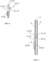
FIG. 8 is a perspective view of an illustrative mounting contact of the printed circuit board wafer ofFIG. 6 . -
FIG. 9 is a cross-section view of the mounting contact ofFIG. 8 mounted in the printed circuit board ofFIG. 6 . -
FIG. 10 is a front perspective view of another alternate illustrative printed circuit board wafer. -
FIG. 11 is a back perspective view of the printed circuit board wafer ofFIG. 10 . -
FIG. 12 is a perspective view of an illustrative mounting contact of the printed circuit board wafer ofFIG. 10 . -
FIG. 13 is a cross-section view of the mounting contact ofFIG. 12 mounted in the printed circuit board ofFIG. 10 . - An embodiment is directed to a circuit board for use in a modular electrical connector. The circuit board has a first surface and an oppositely facing second surface. Signal pathways are provided on the first surface. The signal pathways have signal pathway ends abutting a mounting end of the circuit board. First ground pathways are provided on the first surface. The first ground pathways are positioned adjacent at least one of the signal pathways. The first ground pathways have first ground pathway ends abutting the mounting end of the circuit board. One or more second ground pathways are provided on the second surface. The one or more second ground pathways have second ground pathway ends abutting the mounting end of the circuit board. The positioning of the signal pathway ends abutting the mounting end, the positioning of the first ground pathway ends abutting the mounting end and the positioning of the second ground pathway ends abutting the mounting end minimizes or reduces cross-talk between signal pairs.
- An embodiment is directed to a modular electrical connector with a housing having modules positioned therein. The modules have circuit boards. The circuit boards include first surfaces and oppositely facing second surfaces. Signal pathways are provided on the first surfaces. The signal pathways have signal pathway ends abutting mounting ends of the circuit boards. First ground pathways are provided on the first surfaces. Each of the first ground pathways are positioned adjacent at least one of the signal pathways. The first ground pathways have first ground pathway ends abutting the mounting ends of the circuit boards. One or more second ground pathways are provided on the second surfaces. The one or more second ground pathways have second ground pathway ends abutting the mounting ends of the circuit boards. Signal mounting contacts and ground mating contacts are provided at the mating ends of the circuit boards. The positioning of the signal pathway ends abutting the mounting ends, the positioning of the first ground pathway ends abutting the mounting ends and the positioning of the second ground pathway ends abutting the mounting ends reduces cross-talk between differential signal pairs of the signal pathways.
-
FIG. 1 illustrates anelectrical connector 10 formed in accordance with an illustrative embodiment. In the illustrative embodiment, theelectrical connector 10 is a daughtercard connector that can be mated to a mating backplane connector (not shown) to electrically connect a backplane circuit board (not shown) and a daughtercard circuit board (not shown). While theelectrical connector 10 is described herein with reference to a daughtercard connector, it is realized that the subject matter herein may be utilized with different types of electrical connectors other than a daughtercard connector. Thedaughtercard connector 10 is merely illustrative of an illustrative embodiment of the type ofelectrical connector 10 that mates with a mating connector. - In the illustrative embodiment shown, the
connector 10 constitutes a right angle connector wherein amating end 16 and mountingend 18 of theconnector 10 are oriented perpendicular to one another. Theconnector 10 is mounted to the daughtercard circuit board (not shown) at themounting end 18. Theconnector 10 is mounted to the mating connector (not shown) at themating end 16. Other orientations of theends - As shown in the illustrative embodiment shown in
FIGS. 2 through 5 , theconnector 10 includes ahousing 38 which is made from a plurality ofmodules 40. Each of themodules 40 has a circuit board orsubstrate 45. - As shown in
FIG. 2 , each of thesubstrate 45 has a mating end 24 configured to mate with the mating connector (not shown) and amounting end 46 which is configured to mount to the daughtercard circuit board (not shown). Thesubstrates 45 hold a plurality ofindividual signal pathways 47 which include matingsignal contact pads 48, signal traces 49 and mountingsignal contacts 50. The matingsignal contact pads 48 are mechanically and electrically connected to the signal traces 49 by known methods. The mountingsignal contacts 50 are mechanically and electrically connected to the signal traces 49 by known methods, such as but not limited to soldering, as will be more fully described. Thesignal pathways 47 extend from proximate themating end 42 to the mountingend 46. Ends 60 of the signal traces 49 are positioned in line or abut the mountingend 46 of thesubstrate 45. In an exemplary embodiment, thesignal pathways 47 are arranged in pairs carrying differential signals. Theindividual signal pathways 47 are positioned on afirst surface 55 of thecircuit boards 45. - Each of the
substrates 45 of themodules 40 holds a plurality offirst ground pathways 51 which include matingground contact pads 52, ground traces 53 and mountingground contacts 54. The mountingground contacts 54 are mechanically and electrically connected to the ground traces 53 by known methods, such as but not limited to soldering to a conductive pad of the ground traces 53. Theground pathways 51 extend from proximate themating end 42 to the mountingend 46. Ends 61 of the ground traces 53 are positioned in line or abut the mountingend 46 of thesubstrate 45. Theindividual ground pathways 51 are positioned on thefirst surface 55 of eachmodule 40. - As shown in
FIG. 3 , each of thesubstrates 45 of themodules 40 include second ground pathways or traces 56 on asecond surface 57 of eachsubstrate 45. Thesecond surface 57 being opposed and spaced from thefirst surface 55. The ground traces 56 extend from proximate themating end 42 to the mountingend 46. Ends 63 of the ground traces 56 are positioned in line or abut the mountingend 46 of thesubstrate 45. -
First openings 64 are provided proximate the mountingend 46 of thesubstrate 45. Theopenings 64 are positioned in the signal traces 49 and extend from thefirst surface 55 to thesecond surface 57. In the illustrative embodiment shown, theopenings 64 are provided in electrical engagement with the signal traces 49, but are not provided in electrical engagement with the ground traces 56 on thesecond surface 57. -
Second openings 65 are provided proximate the mountingend 46 of thesubstrate 45. Theopenings 65 are positioned in the ground traces 53 and extend from thefirst surface 55 to thesecond surface 57. In the illustrative embodiment shown, theopenings 65 are provided in electrical engagement with the ground traces 53 and the ground traces 56 on thesecond surface 57. - The mounting
signal contacts 50 have mounting members 73 and compliant portions 78. The mounting members 73 are configured to be positioned in theopenings 64 through thefirst surfaces 55 of thesubstrates 45. The mounting members 73 of the mountingsignal contacts 50 are mechanically and electrically mounted in theopenings 64 and connected to the signal traces 49 by known methods, such as but not limited to soldering, The compliant portions 78 are configured to engage the daughtercard (not shown). The compliant portions 78 may be, but are not limited to, an eye of the needle pin, although other configurations may be used. - The mounting
ground contacts 54 have mounting members 86 and compliant portions 87. The mounting members 86 are configured to be positioned in theopenings 65 through thefirst surfaces 55 of thesubstrates 45. The mounting members 86 of the mountingground contacts 54 are mechanically and electrically mounted in theopenings 65 and connected to the ground traces 53 and the ground traces 56 by known methods, such as but not limited to soldering, The compliant portions 87 are configured to engage the daughtercard (not shown). The compliant portions 87 may be, but are not limited to, an eye of the needle pin, although other configurations may be used. - The combination of the
ground pathways 51 and the ground traces 56 surround the pairs ofsignal pathways 47. As theground pathways 51 and the ground traces 56 are electrically commoned together, theground pathways 51 and the ground traces 56 provide electrical shielding and reduce cross-talk between the pairs ofsignal pathways 47. - In the illustrative embodiment shown in
FIG. 1 , thehousing 38 of theconnector 10 has fourmodules 40 which are positioned adjacent to each other. However, other numbers of modules may be used. Eachmodule 40 is spaced fromadjacent modules 40 to provide mating slots 62 for receiving portions of the mating connector. - With the
housing 38 properly assembled, theground pathways 51 and the ground traces 56 ofadjacent modules 40 extend about the periphery of the pairs ofsignal pathways 47 and surround the pairs ofsignal pathways 47 to provide electrical shielding for the pairs ofsignal pathways 47. In an exemplary embodiment, entire, 360 degree shielding is provided by theground pathways 51 and the ground traces 56 along the length of thesignal pathways 47. Theground pathways 51 and the ground traces 56 may control electrical characteristics at the mating ends and throughout thehousing 38, such as by controlling cross-talk, signal radiation or other electrical characteristics. - As the ends 60 of the signal traces 49, the ends 61 of the ground traces 53 and the
ends 63 of the ground traces 56 are positioned in line or abut the mountingend 46 of thesubstrate 45 the amount of ground that is present on thesubstrates 45 and theconnector 10 is maximized, which in turn minimizes cross-talk between signal pairs. In addition, as theopenings 64 andopenings 65 are positioned proximate to the mountingend 46, the length of the mounting members 73 of the mountingsignal contacts 50 and the length of the mounting members 86 of the mountingground contacts 54 is minimized, which also reduces the cross-talk between signal pairs. - As shown in a first alternate illustrative embodiment illustrated in
FIGS. 6 through 9 , the mountingsignal contacts 150 have mounting members 173 and compliant portions 178. The mounting members 173 have signal trace engaging members 179 and support members 180. The signal trace engaging members 179 are mechanically and electrically mounted and connected to the ends of the signal traces 49 by known methods, such as but not limited to soldering. The support members 180 extend at approximately right angles to the signal trace engaging members 179. The support members 180 have support surfaces 181 which cooperate with the mountingend 46 of thesubstrate 45 to properly locate the mountingsignal contacts 150 and to provide support to thesubstrate 45 and the mountingsignal contacts 150. The compliant portions 178 are configured to engage the daughtercard (not shown). The compliant portions 178 may be, but are not limited to, an eye of the needle pin, although other configurations may be used. - The mounting
ground contacts 154 have mounting members 186 and compliant portions 187. The mounting members 186 have ground trace engaging members 182 and support members 183. The ground trace engaging members 182 are mechanically and electrically mounted and connected to the ends of the ground traces 56 by known methods, such as but not limited to soldering. The support members 183 extend at approximately right angles to the ground trace engaging members 182. The support members 183 have support surfaces 184 which cooperate with the mountingend 46 of thesubstrate 45 to properly locate the mountingground contacts 154 and to provide support to thesubstrate 45 and the mountingground contacts 154. The compliant portions 187 are configured to engage the daughtercard (not shown). The compliant portions 187 may be, but are not limited to, an eye of the needle pin, although other configurations may be used. - As shown in a second alternate illustrative embodiment illustrated in
FIGS. 10 through 13 , the mountingsignal contacts 250 have mounting members 273 and compliant portions 278. The mounting members 273 have signal trace engaging members 279 and support members 280. The support members 280 have support surfaces 281 which cooperate with the mountingend 46 of thesubstrate 45 to properly locate the mountingsignal contacts 250 and to provide support to thesubstrate 45 and the mountingsignal contacts 250. The support surfaces 281 are electrically insulated from the ground surfaces of thesubstrate 45. Examples of how to provide the insulation include, but are not limited to, removing the ground surface of thesubstrate 45 or adding an insulative surface over the ground surface of thesubstrate 45. The signal trace engaging members 279 extend from the support members 280 and are mechanically and electrically mounted and connected to the ends of the signal traces 49 by known methods, such as, but not limited to, pressure applied by the compliant beam of the signal trace engaging member 279 or by soldering. The compliant portions 278 are configured to engage the daughtercard (not shown). The compliant portions 278 may be, but are not limited to, an eye of the needle pin, although other configurations may be used. - The mounting
ground contacts 254 have mounting members 286 and compliant portions 287. The mounting members 286 have ground trace engaging members 282 and support members 283. The support members 283 have support surfaces 284 which cooperate with the mountingend 46 of thesubstrate 45 to properly locate the mountingground contacts 254 and to provide support to thesubstrate 45 and the mountingground contacts 254. The ground trace engaging members 282 extend from the support members 283 and are mechanically and electrically mounted and connected to the ends of the ground traces 56 by known methods, such as, but not limited to, pressure applied by the compliant beam of the ground trace engaging member 282 or by soldering. The compliant portions 287 are configured to engage the daughtercard (not shown). The compliant portions 287 may be, but are not limited to, an eye of the needle pin, although other configurations may be used.
Claims (12)
- A circuit board (45) for use in a modular electrical connector (10), the circuit board (45) comprising:a first surface (55) and an oppositely facing second surface (57);signal pathways (47) provided on the first surface (55), the signal pathways (47) having signal pathway ends (60) abutting a mounting end (46) of the circuit board (45);first ground pathways (51) provided on the first surface (55), each of the first ground pathways (51) positioned adjacent at least one of the signal pathways (47), the first ground pathways (51) having first ground pathway ends (61) abutting the mounting end (46) of the circuit board (45);one or more second ground pathways (56) provided on the second surface (57), the one or more second ground pathways (56) having second ground pathway ends (63) abutting the mounting end (46) of the circuit board (45);wherein the positioning of the signal pathway ends (60) abutting the mounting end (46), the positioning of the first ground pathway ends (61) abutting the mounting end (46) and the positioning of the second ground pathway ends (63) abutting the mounting end (46) reduces cross-talk between signal pairs.
- The circuit board (45) as recited in claim 1, wherein the signal pathways (47) have mating signal contact pads (48), signal traces (49) and mounting signal contacts (50), the signal traces (49) extend from proximate a mating end (42) of the circuit board (45) to abutting the mounting end (46) of the circuit board (45).
- The circuit board (45) as recited in claim 1 or 2, wherein the signal pathways (47) are arranged in pairs carrying differential signals.
- The circuit board (45) as recited in any preceding claim, wherein the first ground pathways (51) have first mating ground contact pads (52), first ground traces (53) and first mounting ground contacts (54), the first ground traces (53) extend from proximate the mating end (42) to abutting the mounting end (46) of the circuit board (45).
- The circuit board (45) as recited in any preceding claim, wherein the second ground pathways (56) have second ground traces (56), the second ground traces (56) extend from proximate a mating end (42) of the circuit board (45) to abutting the mounting end (46) of the circuit board (45).
- The circuit board (45) as recited in claim 5, wherein first openings (64) are provided proximate the mounting end (46) of the circuit board (45), the first openings (64) are positioned in the signal traces (49) and extend from the first surface (55) to the second surface (57), the first openings (64) are provided in electrical engagement with the signal traces (49).
- The circuit board (45) as recited in claim 6, wherein second openings (65) are provided proximate the mounting end (46) of the circuit board (45), the second openings (65) are positioned in the first ground traces (53) and the second ground traces (56) and extend from the first surface (55) to the second surface (57), the second openings (65) are provided in electrical engagement with the first ground traces (53) and the second ground traces (56).
- The circuit board (45) as recited in claim 7, wherein the mounting signal contacts (50) have mounting members (73) and compliant portions (78), the mounting members (73) are positioned in the first openings (64) through the first surface (55) of the circuit board (45).
- The circuit board (45) as recited in claim 8, wherein the mounting ground contacts (54) have mounting members (86) and compliant portions (87), the mounting members (86) are positioned in the second openings (65) through the first surface (55) of the circuit board (45).
- The circuit board (45) as recited in claims 2 and 4 or any claim depending on claims 2 and 4, wherein the mounting signal contacts (150) and the mounting ground contacts (154) have mounting members (173, 186) and compliant portions (178, 187), the mounting members (173, 186) have trace engaging members (179, 182) and support members (180, 183), the support members (180, 183) extend at approximately right angles to the trace engaging members (179, 182).
- The circuit board (45) as recited in claim 10, wherein the support members (180, 183) have support surfaces (181, 184) which cooperate with the mounting end (46) of the circuit board (45) to properly locate the mounting signal contacts (150) and the mounting ground contacts (154) and to provide support to the circuit board (45) and the mounting signal contacts (150) and the mounting ground contacts (154).
- The circuit board (45) as recited in claim 10 or 11, wherein the trace engaging members (179, 182) extend from the support members (180, 183).
Applications Claiming Priority (1)
| Application Number | Priority Date | Filing Date | Title |
|---|---|---|---|
| US16/830,581 US11264749B2 (en) | 2020-03-26 | 2020-03-26 | Modular connector with printed circuit board wafer to reduce crosstalk |
Publications (2)
| Publication Number | Publication Date |
|---|---|
| EP3886270A1 true EP3886270A1 (en) | 2021-09-29 |
| EP3886270B1 EP3886270B1 (en) | 2024-12-18 |
Family
ID=75143465
Family Applications (1)
| Application Number | Title | Priority Date | Filing Date |
|---|---|---|---|
| EP21163861.4A Active EP3886270B1 (en) | 2020-03-26 | 2021-03-22 | Modular connector with printed circuit board wafer to reduce cross-talk |
Country Status (2)
| Country | Link |
|---|---|
| US (1) | US11264749B2 (en) |
| EP (1) | EP3886270B1 (en) |
Families Citing this family (1)
| Publication number | Priority date | Publication date | Assignee | Title |
|---|---|---|---|---|
| CN115021031B (en) * | 2022-06-21 | 2025-12-02 | 四川华丰科技股份有限公司 | Signal transmission module and female connector |
Citations (2)
| Publication number | Priority date | Publication date | Assignee | Title |
|---|---|---|---|---|
| US6875031B1 (en) * | 2003-12-05 | 2005-04-05 | Hon Hai Precision Ind. Co., Ltd. | Electrical connector with circuit board module |
| US20170358881A1 (en) * | 2016-06-10 | 2017-12-14 | Te Connectivity Corporation | Electrical contact pad for electrically contacting a connector |
Family Cites Families (25)
| Publication number | Priority date | Publication date | Assignee | Title |
|---|---|---|---|---|
| US6663442B1 (en) | 2000-01-27 | 2003-12-16 | Tyco Electronics Corporation | High speed interconnect using printed circuit board with plated bores |
| US6824391B2 (en) | 2000-02-03 | 2004-11-30 | Tyco Electronics Corporation | Electrical connector having customizable circuit board wafers |
| US6267604B1 (en) | 2000-02-03 | 2001-07-31 | Tyco Electronics Corporation | Electrical connector including a housing that holds parallel circuit boards |
| US6171115B1 (en) | 2000-02-03 | 2001-01-09 | Tyco Electronics Corporation | Electrical connector having circuit boards and keying for different types of circuit boards |
| AU2001264942A1 (en) | 2000-05-25 | 2001-12-03 | Tyco Electronics Corporation | Electrical connector having contacts isolated by shields |
| US6540522B2 (en) * | 2001-04-26 | 2003-04-01 | Tyco Electronics Corporation | Electrical connector assembly for orthogonally mating circuit boards |
| US6384341B1 (en) | 2001-04-30 | 2002-05-07 | Tyco Electronics Corporation | Differential connector footprint for a multi-layer circuit board |
| US6488549B1 (en) | 2001-06-06 | 2002-12-03 | Tyco Electronics Corporation | Electrical connector assembly with separate arcing zones |
| US6582250B2 (en) | 2001-11-20 | 2003-06-24 | Tyco Electronics Corporation | Connector module organizer |
| US6663426B2 (en) | 2002-01-09 | 2003-12-16 | Tyco Electronics Corporation | Floating interface for electrical connector |
| US6655966B2 (en) | 2002-03-19 | 2003-12-02 | Tyco Electronics Corporation | Modular connector with grounding interconnect |
| US6705895B2 (en) | 2002-04-25 | 2004-03-16 | Tyco Electronics Corporation | Orthogonal interface for connecting circuit boards carrying differential pairs |
| US6890214B2 (en) | 2002-08-21 | 2005-05-10 | Tyco Electronics Corporation | Multi-sequenced contacts from single lead frame |
| US6808399B2 (en) | 2002-12-02 | 2004-10-26 | Tyco Electronics Corporation | Electrical connector with wafers having split ground planes |
| US6811414B1 (en) | 2003-05-16 | 2004-11-02 | Tyco Electronics Corporation | Electrical connector module with multiple card edge sections |
| US6811440B1 (en) | 2003-08-29 | 2004-11-02 | Tyco Electronics Corporation | Power connector |
| US6884117B2 (en) * | 2003-08-29 | 2005-04-26 | Hon Hai Precision Ind. Co., Ltd. | Electrical connector having circuit board modules positioned between metal stiffener and a housing |
| US6964583B2 (en) | 2004-02-13 | 2005-11-15 | Tyco Electronics Corporation | Connector having low frequency noise reducing ground |
| US6932649B1 (en) | 2004-03-19 | 2005-08-23 | Tyco Electronics Corporation | Active wafer for improved gigabit signal recovery, in a serial point-to-point architecture |
| US6997736B2 (en) | 2004-03-26 | 2006-02-14 | Tyco Electronics Corporation | Guide receptacle with tandem mounting features |
| US6945810B1 (en) | 2004-04-28 | 2005-09-20 | Tyco Electronics Corporation | Double ended guide pin for keying on both sides of a circuit board |
| US7044794B2 (en) | 2004-07-14 | 2006-05-16 | Tyco Electronics Corporation | Electrical connector with ESD protection |
| US7175445B2 (en) | 2004-08-31 | 2007-02-13 | Tyco Electronics Corporation | Electrical connector power wafers |
| US8840431B2 (en) | 2012-10-26 | 2014-09-23 | Tyco Electronics Corporation | Electrical connector systems |
| US10535971B2 (en) | 2017-10-12 | 2020-01-14 | Te Connectivity Corporation | Electrical connector |
-
2020
- 2020-03-26 US US16/830,581 patent/US11264749B2/en active Active
-
2021
- 2021-03-22 EP EP21163861.4A patent/EP3886270B1/en active Active
Patent Citations (2)
| Publication number | Priority date | Publication date | Assignee | Title |
|---|---|---|---|---|
| US6875031B1 (en) * | 2003-12-05 | 2005-04-05 | Hon Hai Precision Ind. Co., Ltd. | Electrical connector with circuit board module |
| US20170358881A1 (en) * | 2016-06-10 | 2017-12-14 | Te Connectivity Corporation | Electrical contact pad for electrically contacting a connector |
Also Published As
| Publication number | Publication date |
|---|---|
| EP3886270B1 (en) | 2024-12-18 |
| US11264749B2 (en) | 2022-03-01 |
| US20210305737A1 (en) | 2021-09-30 |
Similar Documents
| Publication | Publication Date | Title |
|---|---|---|
| US11081821B2 (en) | Direct mate cable assembly | |
| EP3890120B1 (en) | Modular electrical connector with additional grounding | |
| US5228864A (en) | Connectors with ground structure | |
| EP3890119B1 (en) | Shield component for use with modular electrical connector to reduce cross-talk | |
| US10170882B2 (en) | Direct-attach connector | |
| EP0676833B1 (en) | Surface mountable card edge connector | |
| US10923843B1 (en) | Receptacle assembly having cabled receptacle connector | |
| EP3886261B1 (en) | Modular electrical connector with reduced cross-talk | |
| US20240313476A1 (en) | Ground Shield Contact Member | |
| WO2009055242A2 (en) | Electrical connector assembly | |
| US20190150311A1 (en) | Socket connector for an electronic package | |
| US7059907B2 (en) | Modular electrical connector | |
| EP3886268A1 (en) | Modular electrical connector with conductive coating to reduce cross-talk | |
| US12322887B2 (en) | Circuit board wafer with contacts mounted on castellated edges | |
| EP3886269B1 (en) | Modular printed circuit board wafer connector with reduced cross-talk | |
| EP3886270B1 (en) | Modular connector with printed circuit board wafer to reduce cross-talk | |
| EP4362241A1 (en) | Ground shields positioned between columns of contacts | |
| US20240145994A1 (en) | Interconnection System for Ground Current Optimization | |
| EP4362240B1 (en) | Contact and shield configuration for ground current optimization | |
| US12586944B2 (en) | Electrical connector with angled contacts with arrangement for controlling crosstalk | |
| EP4681293A1 (en) | Ground shield contact member |
Legal Events
| Date | Code | Title | Description |
|---|---|---|---|
| PUAI | Public reference made under article 153(3) epc to a published international application that has entered the european phase |
Free format text: ORIGINAL CODE: 0009012 |
|
| STAA | Information on the status of an ep patent application or granted ep patent |
Free format text: STATUS: THE APPLICATION HAS BEEN PUBLISHED |
|
| AK | Designated contracting states |
Kind code of ref document: A1 Designated state(s): AL AT BE BG CH CY CZ DE DK EE ES FI FR GB GR HR HU IE IS IT LI LT LU LV MC MK MT NL NO PL PT RO RS SE SI SK SM TR |
|
| STAA | Information on the status of an ep patent application or granted ep patent |
Free format text: STATUS: REQUEST FOR EXAMINATION WAS MADE |
|
| 17P | Request for examination filed |
Effective date: 20220328 |
|
| RBV | Designated contracting states (corrected) |
Designated state(s): AL AT BE BG CH CY CZ DE DK EE ES FI FR GB GR HR HU IE IS IT LI LT LU LV MC MK MT NL NO PL PT RO RS SE SI SK SM TR |
|
| RAP1 | Party data changed (applicant data changed or rights of an application transferred) |
Owner name: TE CONNECTIVITY SOLUTIONS GMBH |
|
| STAA | Information on the status of an ep patent application or granted ep patent |
Free format text: STATUS: EXAMINATION IS IN PROGRESS |
|
| 17Q | First examination report despatched |
Effective date: 20231004 |
|
| GRAP | Despatch of communication of intention to grant a patent |
Free format text: ORIGINAL CODE: EPIDOSNIGR1 |
|
| STAA | Information on the status of an ep patent application or granted ep patent |
Free format text: STATUS: GRANT OF PATENT IS INTENDED |
|
| RIC1 | Information provided on ipc code assigned before grant |
Ipc: H05K 3/32 20060101ALN20240802BHEP Ipc: H01R 12/58 20110101ALN20240802BHEP Ipc: H05K 3/34 20060101ALI20240802BHEP Ipc: H05K 1/11 20060101ALI20240802BHEP Ipc: H05K 1/02 20060101ALI20240802BHEP Ipc: H01P 5/02 20060101ALI20240802BHEP Ipc: H01R 13/6587 20110101ALI20240802BHEP Ipc: H01R 13/6471 20110101AFI20240802BHEP |
|
| INTG | Intention to grant announced |
Effective date: 20240828 |
|
| GRAS | Grant fee paid |
Free format text: ORIGINAL CODE: EPIDOSNIGR3 |
|
| GRAA | (expected) grant |
Free format text: ORIGINAL CODE: 0009210 |
|
| STAA | Information on the status of an ep patent application or granted ep patent |
Free format text: STATUS: THE PATENT HAS BEEN GRANTED |
|
| AK | Designated contracting states |
Kind code of ref document: B1 Designated state(s): AL AT BE BG CH CY CZ DE DK EE ES FI FR GB GR HR HU IE IS IT LI LT LU LV MC MK MT NL NO PL PT RO RS SE SI SK SM TR |
|
| REG | Reference to a national code |
Ref country code: CH Ref legal event code: EP |
|
| REG | Reference to a national code |
Ref country code: DE Ref legal event code: R096 Ref document number: 602021023423 Country of ref document: DE |
|
| REG | Reference to a national code |
Ref country code: IE Ref legal event code: FG4D |
|
| REG | Reference to a national code |
Ref country code: LT Ref legal event code: MG9D |
|
| PG25 | Lapsed in a contracting state [announced via postgrant information from national office to epo] |
Ref country code: HR Free format text: LAPSE BECAUSE OF FAILURE TO SUBMIT A TRANSLATION OF THE DESCRIPTION OR TO PAY THE FEE WITHIN THE PRESCRIBED TIME-LIMIT Effective date: 20241218 |
|
| PG25 | Lapsed in a contracting state [announced via postgrant information from national office to epo] |
Ref country code: FI Free format text: LAPSE BECAUSE OF FAILURE TO SUBMIT A TRANSLATION OF THE DESCRIPTION OR TO PAY THE FEE WITHIN THE PRESCRIBED TIME-LIMIT Effective date: 20241218 |
|
| PG25 | Lapsed in a contracting state [announced via postgrant information from national office to epo] |
Ref country code: BG Free format text: LAPSE BECAUSE OF FAILURE TO SUBMIT A TRANSLATION OF THE DESCRIPTION OR TO PAY THE FEE WITHIN THE PRESCRIBED TIME-LIMIT Effective date: 20241218 |
|
| PG25 | Lapsed in a contracting state [announced via postgrant information from national office to epo] |
Ref country code: NO Free format text: LAPSE BECAUSE OF FAILURE TO SUBMIT A TRANSLATION OF THE DESCRIPTION OR TO PAY THE FEE WITHIN THE PRESCRIBED TIME-LIMIT Effective date: 20250318 |
|
| REG | Reference to a national code |
Ref country code: NL Ref legal event code: MP Effective date: 20241218 |
|
| PG25 | Lapsed in a contracting state [announced via postgrant information from national office to epo] |
Ref country code: LV Free format text: LAPSE BECAUSE OF FAILURE TO SUBMIT A TRANSLATION OF THE DESCRIPTION OR TO PAY THE FEE WITHIN THE PRESCRIBED TIME-LIMIT Effective date: 20241218 Ref country code: GR Free format text: LAPSE BECAUSE OF FAILURE TO SUBMIT A TRANSLATION OF THE DESCRIPTION OR TO PAY THE FEE WITHIN THE PRESCRIBED TIME-LIMIT Effective date: 20250319 |
|
| PG25 | Lapsed in a contracting state [announced via postgrant information from national office to epo] |
Ref country code: RS Free format text: LAPSE BECAUSE OF FAILURE TO SUBMIT A TRANSLATION OF THE DESCRIPTION OR TO PAY THE FEE WITHIN THE PRESCRIBED TIME-LIMIT Effective date: 20250318 |
|
| PG25 | Lapsed in a contracting state [announced via postgrant information from national office to epo] |
Ref country code: NL Free format text: LAPSE BECAUSE OF FAILURE TO SUBMIT A TRANSLATION OF THE DESCRIPTION OR TO PAY THE FEE WITHIN THE PRESCRIBED TIME-LIMIT Effective date: 20241218 |
|
| REG | Reference to a national code |
Ref country code: AT Ref legal event code: MK05 Ref document number: 1753025 Country of ref document: AT Kind code of ref document: T Effective date: 20241218 |
|
| PG25 | Lapsed in a contracting state [announced via postgrant information from national office to epo] |
Ref country code: SM Free format text: LAPSE BECAUSE OF FAILURE TO SUBMIT A TRANSLATION OF THE DESCRIPTION OR TO PAY THE FEE WITHIN THE PRESCRIBED TIME-LIMIT Effective date: 20241218 |
|
| PG25 | Lapsed in a contracting state [announced via postgrant information from national office to epo] |
Ref country code: PL Free format text: LAPSE BECAUSE OF FAILURE TO SUBMIT A TRANSLATION OF THE DESCRIPTION OR TO PAY THE FEE WITHIN THE PRESCRIBED TIME-LIMIT Effective date: 20241218 |
|
| PG25 | Lapsed in a contracting state [announced via postgrant information from national office to epo] |
Ref country code: ES Free format text: LAPSE BECAUSE OF FAILURE TO SUBMIT A TRANSLATION OF THE DESCRIPTION OR TO PAY THE FEE WITHIN THE PRESCRIBED TIME-LIMIT Effective date: 20241218 |
|
| PG25 | Lapsed in a contracting state [announced via postgrant information from national office to epo] |
Ref country code: IS Free format text: LAPSE BECAUSE OF FAILURE TO SUBMIT A TRANSLATION OF THE DESCRIPTION OR TO PAY THE FEE WITHIN THE PRESCRIBED TIME-LIMIT Effective date: 20250418 |
|
| PG25 | Lapsed in a contracting state [announced via postgrant information from national office to epo] |
Ref country code: PT Free format text: LAPSE BECAUSE OF FAILURE TO SUBMIT A TRANSLATION OF THE DESCRIPTION OR TO PAY THE FEE WITHIN THE PRESCRIBED TIME-LIMIT Effective date: 20250421 |
|
| PG25 | Lapsed in a contracting state [announced via postgrant information from national office to epo] |
Ref country code: EE Free format text: LAPSE BECAUSE OF FAILURE TO SUBMIT A TRANSLATION OF THE DESCRIPTION OR TO PAY THE FEE WITHIN THE PRESCRIBED TIME-LIMIT Effective date: 20241218 |
|
| PG25 | Lapsed in a contracting state [announced via postgrant information from national office to epo] |
Ref country code: RO Free format text: LAPSE BECAUSE OF FAILURE TO SUBMIT A TRANSLATION OF THE DESCRIPTION OR TO PAY THE FEE WITHIN THE PRESCRIBED TIME-LIMIT Effective date: 20241218 Ref country code: AT Free format text: LAPSE BECAUSE OF FAILURE TO SUBMIT A TRANSLATION OF THE DESCRIPTION OR TO PAY THE FEE WITHIN THE PRESCRIBED TIME-LIMIT Effective date: 20241218 |
|
| PG25 | Lapsed in a contracting state [announced via postgrant information from national office to epo] |
Ref country code: SK Free format text: LAPSE BECAUSE OF FAILURE TO SUBMIT A TRANSLATION OF THE DESCRIPTION OR TO PAY THE FEE WITHIN THE PRESCRIBED TIME-LIMIT Effective date: 20241218 |
|
| PG25 | Lapsed in a contracting state [announced via postgrant information from national office to epo] |
Ref country code: CZ Free format text: LAPSE BECAUSE OF FAILURE TO SUBMIT A TRANSLATION OF THE DESCRIPTION OR TO PAY THE FEE WITHIN THE PRESCRIBED TIME-LIMIT Effective date: 20241218 |
|
| PG25 | Lapsed in a contracting state [announced via postgrant information from national office to epo] |
Ref country code: IT Free format text: LAPSE BECAUSE OF FAILURE TO SUBMIT A TRANSLATION OF THE DESCRIPTION OR TO PAY THE FEE WITHIN THE PRESCRIBED TIME-LIMIT Effective date: 20241218 |
|
| PG25 | Lapsed in a contracting state [announced via postgrant information from national office to epo] |
Ref country code: SE Free format text: LAPSE BECAUSE OF FAILURE TO SUBMIT A TRANSLATION OF THE DESCRIPTION OR TO PAY THE FEE WITHIN THE PRESCRIBED TIME-LIMIT Effective date: 20241218 |
|
| REG | Reference to a national code |
Ref country code: DE Ref legal event code: R097 Ref document number: 602021023423 Country of ref document: DE |
|
| PG25 | Lapsed in a contracting state [announced via postgrant information from national office to epo] |
Ref country code: DK Free format text: LAPSE BECAUSE OF FAILURE TO SUBMIT A TRANSLATION OF THE DESCRIPTION OR TO PAY THE FEE WITHIN THE PRESCRIBED TIME-LIMIT Effective date: 20241218 |
|
| PG25 | Lapsed in a contracting state [announced via postgrant information from national office to epo] |
Ref country code: MC Free format text: LAPSE BECAUSE OF FAILURE TO SUBMIT A TRANSLATION OF THE DESCRIPTION OR TO PAY THE FEE WITHIN THE PRESCRIBED TIME-LIMIT Effective date: 20241218 |
|
| PLBE | No opposition filed within time limit |
Free format text: ORIGINAL CODE: 0009261 |
|
| REG | Reference to a national code |
Ref country code: CH Ref legal event code: H13 Free format text: ST27 STATUS EVENT CODE: U-0-0-H10-H13 (AS PROVIDED BY THE NATIONAL OFFICE) Effective date: 20251024 |
|
| STAA | Information on the status of an ep patent application or granted ep patent |
Free format text: STATUS: NO OPPOSITION FILED WITHIN TIME LIMIT |
|
| PG25 | Lapsed in a contracting state [announced via postgrant information from national office to epo] |
Ref country code: LU Free format text: LAPSE BECAUSE OF NON-PAYMENT OF DUE FEES Effective date: 20250322 |
|
| 26N | No opposition filed |
Effective date: 20250919 |
|
| REG | Reference to a national code |
Ref country code: BE Ref legal event code: MM Effective date: 20250331 |
|
| PGFP | Annual fee paid to national office [announced via postgrant information from national office to epo] |
Ref country code: FR Payment date: 20251231 Year of fee payment: 6 |
|
| PG25 | Lapsed in a contracting state [announced via postgrant information from national office to epo] |
Ref country code: BE Free format text: LAPSE BECAUSE OF NON-PAYMENT OF DUE FEES Effective date: 20250331 |
|
| PG25 | Lapsed in a contracting state [announced via postgrant information from national office to epo] |
Ref country code: CH Free format text: LAPSE BECAUSE OF NON-PAYMENT OF DUE FEES Effective date: 20250331 |
|
| PG25 | Lapsed in a contracting state [announced via postgrant information from national office to epo] |
Ref country code: IE Free format text: LAPSE BECAUSE OF NON-PAYMENT OF DUE FEES Effective date: 20250322 |
|
| PGFP | Annual fee paid to national office [announced via postgrant information from national office to epo] |
Ref country code: GB Payment date: 20260106 Year of fee payment: 6 |
|
| PGFP | Annual fee paid to national office [announced via postgrant information from national office to epo] |
Ref country code: DE Payment date: 20260102 Year of fee payment: 6 |
|
| PG25 | Lapsed in a contracting state [announced via postgrant information from national office to epo] |
Ref country code: CY Free format text: LAPSE BECAUSE OF FAILURE TO SUBMIT A TRANSLATION OF THE DESCRIPTION OR TO PAY THE FEE WITHIN THE PRESCRIBED TIME-LIMIT Effective date: 20241218 |
|
| PG25 | Lapsed in a contracting state [announced via postgrant information from national office to epo] |
Ref country code: LT Free format text: LAPSE BECAUSE OF FAILURE TO SUBMIT A TRANSLATION OF THE DESCRIPTION OR TO PAY THE FEE WITHIN THE PRESCRIBED TIME-LIMIT Effective date: 20241218 |
|
| PG25 | Lapsed in a contracting state [announced via postgrant information from national office to epo] |
Ref country code: TR Free format text: LAPSE BECAUSE OF FAILURE TO SUBMIT A TRANSLATION OF THE DESCRIPTION OR TO PAY THE FEE WITHIN THE PRESCRIBED TIME-LIMIT Effective date: 20241218 |