EP3886268A1 - Modular electrical connector with conductive coating to reduce cross-talk - Google Patents
Modular electrical connector with conductive coating to reduce cross-talk Download PDFInfo
- Publication number
- EP3886268A1 EP3886268A1 EP21163857.2A EP21163857A EP3886268A1 EP 3886268 A1 EP3886268 A1 EP 3886268A1 EP 21163857 A EP21163857 A EP 21163857A EP 3886268 A1 EP3886268 A1 EP 3886268A1
- Authority
- EP
- European Patent Office
- Prior art keywords
- housing
- ground
- signal
- contacts
- electrical connector
- Prior art date
- Legal status (The legal status is an assumption and is not a legal conclusion. Google has not performed a legal analysis and makes no representation as to the accuracy of the status listed.)
- Granted
Links
Images





Classifications
-
- H—ELECTRICITY
- H01—ELECTRIC ELEMENTS
- H01R—ELECTRICALLY-CONDUCTIVE CONNECTIONS; STRUCTURAL ASSOCIATIONS OF A PLURALITY OF MUTUALLY-INSULATED ELECTRICAL CONNECTING ELEMENTS; COUPLING DEVICES; CURRENT COLLECTORS
- H01R13/00—Details of coupling devices of the kinds covered by groups H01R12/70 or H01R24/00 - H01R33/00
- H01R13/646—Details of coupling devices of the kinds covered by groups H01R12/70 or H01R24/00 - H01R33/00 specially adapted for high-frequency, e.g. structures providing an impedance match or phase match
- H01R13/6461—Means for preventing cross-talk
- H01R13/6471—Means for preventing cross-talk by special arrangement of ground and signal conductors, e.g. GSGS [Ground-Signal-Ground-Signal]
-
- H—ELECTRICITY
- H01—ELECTRIC ELEMENTS
- H01R—ELECTRICALLY-CONDUCTIVE CONNECTIONS; STRUCTURAL ASSOCIATIONS OF A PLURALITY OF MUTUALLY-INSULATED ELECTRICAL CONNECTING ELEMENTS; COUPLING DEVICES; CURRENT COLLECTORS
- H01R13/00—Details of coupling devices of the kinds covered by groups H01R12/70 or H01R24/00 - H01R33/00
- H01R13/46—Bases; Cases
- H01R13/514—Bases; Cases composed as a modular blocks or assembly, i.e. composed of co-operating parts provided with contact members or holding contact members between them
-
- H—ELECTRICITY
- H01—ELECTRIC ELEMENTS
- H01R—ELECTRICALLY-CONDUCTIVE CONNECTIONS; STRUCTURAL ASSOCIATIONS OF A PLURALITY OF MUTUALLY-INSULATED ELECTRICAL CONNECTING ELEMENTS; COUPLING DEVICES; CURRENT COLLECTORS
- H01R13/00—Details of coupling devices of the kinds covered by groups H01R12/70 or H01R24/00 - H01R33/00
- H01R13/648—Protective earth or shield arrangements on coupling devices, e.g. anti-static shielding
- H01R13/658—High frequency shielding arrangements, e.g. against EMI [Electro-Magnetic Interference] or EMP [Electro-Magnetic Pulse]
- H01R13/6581—Shield structure
- H01R13/6585—Shielding material individually surrounding or interposed between mutually spaced contacts
- H01R13/6586—Shielding material individually surrounding or interposed between mutually spaced contacts for separating multiple connector modules
- H01R13/6587—Shielding material individually surrounding or interposed between mutually spaced contacts for separating multiple connector modules for mounting on PCBs
-
- H—ELECTRICITY
- H05—ELECTRIC TECHNIQUES NOT OTHERWISE PROVIDED FOR
- H05K—PRINTED CIRCUITS; CASINGS OR CONSTRUCTIONAL DETAILS OF ELECTRIC APPARATUS; MANUFACTURE OF ASSEMBLAGES OF ELECTRICAL COMPONENTS
- H05K1/00—Printed circuits
- H05K1/02—Details
- H05K1/14—Structural association of two or more printed circuits
- H05K1/144—Stacked arrangements of planar printed circuit boards
-
- H—ELECTRICITY
- H01—ELECTRIC ELEMENTS
- H01R—ELECTRICALLY-CONDUCTIVE CONNECTIONS; STRUCTURAL ASSOCIATIONS OF A PLURALITY OF MUTUALLY-INSULATED ELECTRICAL CONNECTING ELEMENTS; COUPLING DEVICES; CURRENT COLLECTORS
- H01R12/00—Structural associations of a plurality of mutually-insulated electrical connecting elements, specially adapted for printed circuits, e.g. printed circuit boards [PCB], flat or ribbon cables, or like generally planar structures, e.g. terminal strips, terminal blocks; Coupling devices specially adapted for printed circuits, flat or ribbon cables, or like generally planar structures; Terminals specially adapted for contact with, or insertion into, printed circuits, flat or ribbon cables, or like generally planar structures
- H01R12/70—Coupling devices
- H01R12/71—Coupling devices for rigid printing circuits or like structures
- H01R12/712—Coupling devices for rigid printing circuits or like structures co-operating with the surface of the printed circuit or with a coupling device exclusively provided on the surface of the printed circuit
- H01R12/716—Coupling device provided on the PCB
-
- H—ELECTRICITY
- H01—ELECTRIC ELEMENTS
- H01R—ELECTRICALLY-CONDUCTIVE CONNECTIONS; STRUCTURAL ASSOCIATIONS OF A PLURALITY OF MUTUALLY-INSULATED ELECTRICAL CONNECTING ELEMENTS; COUPLING DEVICES; CURRENT COLLECTORS
- H01R12/00—Structural associations of a plurality of mutually-insulated electrical connecting elements, specially adapted for printed circuits, e.g. printed circuit boards [PCB], flat or ribbon cables, or like generally planar structures, e.g. terminal strips, terminal blocks; Coupling devices specially adapted for printed circuits, flat or ribbon cables, or like generally planar structures; Terminals specially adapted for contact with, or insertion into, printed circuits, flat or ribbon cables, or like generally planar structures
- H01R12/70—Coupling devices
- H01R12/71—Coupling devices for rigid printing circuits or like structures
- H01R12/72—Coupling devices for rigid printing circuits or like structures coupling with the edge of the rigid printed circuits or like structures
- H01R12/73—Coupling devices for rigid printing circuits or like structures coupling with the edge of the rigid printed circuits or like structures connecting to other rigid printed circuits or like structures
- H01R12/735—Printed circuits including an angle between each other
- H01R12/737—Printed circuits being substantially perpendicular to each other
-
- H—ELECTRICITY
- H01—ELECTRIC ELEMENTS
- H01R—ELECTRICALLY-CONDUCTIVE CONNECTIONS; STRUCTURAL ASSOCIATIONS OF A PLURALITY OF MUTUALLY-INSULATED ELECTRICAL CONNECTING ELEMENTS; COUPLING DEVICES; CURRENT COLLECTORS
- H01R13/00—Details of coupling devices of the kinds covered by groups H01R12/70 or H01R24/00 - H01R33/00
- H01R13/46—Bases; Cases
- H01R13/502—Bases; Cases composed of different pieces
-
- H—ELECTRICITY
- H01—ELECTRIC ELEMENTS
- H01R—ELECTRICALLY-CONDUCTIVE CONNECTIONS; STRUCTURAL ASSOCIATIONS OF A PLURALITY OF MUTUALLY-INSULATED ELECTRICAL CONNECTING ELEMENTS; COUPLING DEVICES; CURRENT COLLECTORS
- H01R13/00—Details of coupling devices of the kinds covered by groups H01R12/70 or H01R24/00 - H01R33/00
- H01R13/646—Details of coupling devices of the kinds covered by groups H01R12/70 or H01R24/00 - H01R33/00 specially adapted for high-frequency, e.g. structures providing an impedance match or phase match
- H01R13/6473—Impedance matching
-
- H—ELECTRICITY
- H01—ELECTRIC ELEMENTS
- H01R—ELECTRICALLY-CONDUCTIVE CONNECTIONS; STRUCTURAL ASSOCIATIONS OF A PLURALITY OF MUTUALLY-INSULATED ELECTRICAL CONNECTING ELEMENTS; COUPLING DEVICES; CURRENT COLLECTORS
- H01R13/00—Details of coupling devices of the kinds covered by groups H01R12/70 or H01R24/00 - H01R33/00
- H01R13/648—Protective earth or shield arrangements on coupling devices, e.g. anti-static shielding
- H01R13/658—High frequency shielding arrangements, e.g. against EMI [Electro-Magnetic Interference] or EMP [Electro-Magnetic Pulse]
- H01R13/6598—Shield material
- H01R13/6599—Dielectric material made conductive, e.g. plastic material coated with metal
-
- H—ELECTRICITY
- H01—ELECTRIC ELEMENTS
- H01R—ELECTRICALLY-CONDUCTIVE CONNECTIONS; STRUCTURAL ASSOCIATIONS OF A PLURALITY OF MUTUALLY-INSULATED ELECTRICAL CONNECTING ELEMENTS; COUPLING DEVICES; CURRENT COLLECTORS
- H01R24/00—Two-part coupling devices, or either of their cooperating parts, characterised by their overall structure
- H01R24/60—Contacts spaced along planar side wall transverse to longitudinal axis of engagement
-
- H—ELECTRICITY
- H05—ELECTRIC TECHNIQUES NOT OTHERWISE PROVIDED FOR
- H05K—PRINTED CIRCUITS; CASINGS OR CONSTRUCTIONAL DETAILS OF ELECTRIC APPARATUS; MANUFACTURE OF ASSEMBLAGES OF ELECTRICAL COMPONENTS
- H05K1/00—Printed circuits
- H05K1/02—Details
- H05K1/0213—Electrical arrangements not otherwise provided for
- H05K1/0216—Reduction of cross-talk, noise or electromagnetic interference
- H05K1/0218—Reduction of cross-talk, noise or electromagnetic interference by printed shielding conductors, ground planes or power plane
-
- H—ELECTRICITY
- H05—ELECTRIC TECHNIQUES NOT OTHERWISE PROVIDED FOR
- H05K—PRINTED CIRCUITS; CASINGS OR CONSTRUCTIONAL DETAILS OF ELECTRIC APPARATUS; MANUFACTURE OF ASSEMBLAGES OF ELECTRICAL COMPONENTS
- H05K2201/00—Indexing scheme relating to printed circuits covered by H05K1/00
- H05K2201/04—Assemblies of printed circuits
- H05K2201/042—Stacked spaced PCBs; Planar parts of folded flexible circuits having mounted components in between or spaced from each other
-
- H—ELECTRICITY
- H05—ELECTRIC TECHNIQUES NOT OTHERWISE PROVIDED FOR
- H05K—PRINTED CIRCUITS; CASINGS OR CONSTRUCTIONAL DETAILS OF ELECTRIC APPARATUS; MANUFACTURE OF ASSEMBLAGES OF ELECTRICAL COMPONENTS
- H05K2201/00—Indexing scheme relating to printed circuits covered by H05K1/00
- H05K2201/10—Details of components or other objects attached to or integrated in a printed circuit board
- H05K2201/10007—Types of components
- H05K2201/10189—Non-printed connector
Definitions
- the present invention relates to a modular connector with reduced cross-talk.
- the invention relates to a modular connector with surfaces which have a conductive coating applied to an insulative member optimized for impedance.
- the solution is provided by an electrical connector for use in an electrical connector system which controls cross-talk and signal radiation and optimizes impedance.
- the electrical connector includes a plurality of modules having mating ends and mounting ends. Each of the modules of the plurality of modules has a conductive first housing having.
- the first housing has at least one second housing recess provided in a first surface of the first housing.
- the first housing has ground contact receiving channels provided in the first surface of the first housing.
- At least one second housing is provided in the at least one second housing recess.
- the at least one second housing is made of insulative material and has signal contact receiving channels provided in a first surface of the at least one second housing. Signal contacts are positioned in the signal contact receiving channels of the at least one second housing. Ground contacts are positioned in the ground contact receiving channels of the first housing.
- An embodiment is directed to an electrical connector for use in an electrical connector system which controls cross-talk and signal radiation and optimizes impedance.
- the electrical connector includes a plurality of modules having mating ends and mounting ends. Each of the modules of the plurality of modules has a conductive first housing having.
- the first housing has at least one second housing recess provided in a first surface of the first housing.
- the first housing has ground contact receiving channels provided in the first surface of the first housing.
- At least one second housing is provided in the at least one second housing recess.
- the at least one second housing is made of insulative material and has signal contact receiving channels provided in a first surface of the at least one second housing. Signal contacts are positioned in the signal contact receiving channels of the at least one second housing. Ground contacts are positioned in the ground contact receiving channels of the first housing.
- An embodiment is directed to an electrical connector for use in an electrical connector system which controls cross-talk and signal radiation and optimizes impedance.
- the electrical connector includes a plurality of modules having mating ends and mounting ends. Each of the modules of the plurality of modules has a conductive first housing.
- the first housing has at least one second housing recess and ground contact receiving channels. At least one second housing is provided in the at least one second housing recess.
- the at least one second housing is made of insulative material and has signal contact receiving channels.
- Signal contacts are positioned in the signal contact receiving channels of the at least one second housing.
- the signal contacts are arranged in pairs to carry differential signals.
- Ground contacts are positioned in the ground contact receiving channels of the first housing. Respective ground contacts of the ground contacts are positioned adjacent to the at least one second housing and respective signal contacts of the signal contacts.
- An embodiment is directed to an electrical connector for use in an electrical connector system which controls cross-talk and signal radiation and optimizes impedance.
- the electrical connector includes a plurality of modules having mating ends and mounting ends.
- a first housing has at least one second housing recess provided in a first surface of the first housing.
- the first housing has ground shield receiving channels provided in a second surface of the first housing.
- the ground shield receiving channels are aligned with the at least one second housing recess.
- At least one second housing is provided in the at least one second housing recess.
- the at least one second housing is made of insulative material and has signal contact receiving channels.
- Signal contacts are positioned in the signal contact receiving channels of the at least one second housing.
- the signal contacts are arranged in pairs to carry differential signals.
- Ground shield plates are positioned in the ground shield receiving channels of the first housing to engage grounding contacts of a mating connector
- FIGS. 1 through 7 illustrate an electrical connector system 10 formed in accordance with an illustrative embodiment.
- the electrical connector system 10 includes a backplane connector 12 and a daughtercard connector 14 that are used to electrically connect a backplane circuit board (not shown) and a daughtercard circuit board (not shown). While the electrical connector system 10 is described herein with reference to backplane connectors 12 and daughtercard connectors 14, it is realized that the subject matter herein may be utilized with different types of electrical connectors other than a backplane connector or a daughtercard connector.
- the backplane connector 12 and the daughtercard connector 14 are merely illustrative embodiments of an electrical connector system 10 that interconnects a particular type of circuit board, namely a backplane circuit board, with a daughtercard circuit board.
- the daughtercard connector 14 constitutes a right angle connector wherein a mating interface 16 and mounting interface 18 of the daughtercard connector 14 are oriented perpendicular to one another.
- the daughtercard connector 14 is mounted to the daughtercard circuit board at the mounting interface 18.
- Other orientations of the interfaces 16, 18 are possible in alternative embodiments.
- the daughtercard connector 14 includes a housing 24, made of one or more components, holding a plurality of circuit boards 26 therein.
- the circuit boards 26 have pairs 28 of individual signal pathways or traces (not shown) that extend between the mating interface 16 and the mounting interface 18.
- the signal traces have signal conductive pads 32 provided proximate the mating interface 16.
- the signal traces are configured to be mated with and electrically connected to the signal contacts 48 of the backplane connector 12.
- the circuit boards 26 have individual ground pathways or traces that extend between the mating interface 16 and the mounting interface 18.
- the ground traces (not shown) have ground conductive pads 36 provided proximate the mating interface 16.
- the ground traces are configured to be mated with, and electrically connected to, the ground contacts 50 or the shield or ground plates 52 of the backplane connector 12.
- the circuit boards 26 also have ground pathways or traces 35 on opposites sides of the circuit boards 26 from the ground traces.
- the ground traces 35 extend between the mating interface 16 and the mounting interface 18.
- the circuit boards 26 may be contact modules, the signal traces may be mating signal contacts and the ground traces may be ground contacts.
- the backplane connector 12 constitutes a header connector mounted to the backplane circuit board.
- the backplane connector 12 is mated to the daughtercard connector 14.
- the daughtercard circuit board is oriented generally perpendicular with respect to the backplane circuit board.
- the backplane connector 12 includes a mating end 46 and a mounting end 42 that are oriented generally parallel to one another.
- the backplane connector 12 is mounted to the backplane circuit board at the mounting end 42.
- the backplane connector 12 includes a housing 38 which includes a plurality of modules 40.
- Each of the modules 40 has a mating end 46 , also referred to herein as a front end 46 , that is positioned in a recess 44 of the daughtercard connector 14 during mating.
- Each of the modules 40 has a mounting end 42, also referred to herein as a rear end 42, which is mounted to the backplane circuit board.
- Each of the modules 40 holds a plurality of individual signal contacts 48 that extend between the mating end 46 and the mounting end 42. In an exemplary embodiment, the signal contacts 48 are arranged in pairs carrying differential signals.
- Each of the modules 40 also holds a plurality of ground contacts 50 that extend between the mating end 46 and the mounting end 42.
- each module 40 has a conductive first housing 41 and at least one second housing 43.
- the second housing 43 In the illustrative embodiment shown, three second housings 43 are provided, but other numbers and configurations of the second housings 43 may be provided.
- Each of the conductive first housings 41 has a first surface 45 and an oppositely facing second surface 47. At least one second housing receiving recess 49 extends from the first surface 45 toward the second surface 47.
- the first housing 41 is an insulative member made of an insulative material with a conductive coating 51 applied to the outer surfaces of the first housing 41.
- the conductive coating 51 may be applied by known methods or processes, including, but not limited to, an electroless process, an electroplating process or a physical vapor deposition process.
- the conductive coating 51 allows the first housing 41 to act as a shield, as will be more fully described, while allowing the modules 40 and the backplane connector 12 to mate with existing daughtercard connectors 14.
- the shape of the first housing 41 can be molded or manufactured in a shape which optimizes the impedance characteristics of the first housing 41 when the conductive coating 51 is applied.
- the conductive first housings 41 of the modules 40 include a plurality of ground cavities or channels 60 extending between the mating end 46 and the mounting end 42 of the first surface 45.
- the ground channels 60 extend from the first surface 45 toward the second surface 47 along the mating axes and receive the ground contacts 50.
- ground conductive pads 36 of the ground traces of the daughtercard connector 14 are also received in the ground channels 6.
- Any number of ground channels 60 may be provided.
- the ground channels 60 may be provided at any locations within the modules 40 and the housing 38. In an exemplary embodiment, the ground channels 60 are generally positioned adjacent to and/or between the second housing receiving recesses 49.
- the second housings 43 have a first surface 53 and an oppositely facing second surface 55.
- the second housings 43 are insulative members made of an insulative material.
- the second housings 43 may be separate components which are assembled to the first housings 41 using known methods, such as, but not limited to, adhesion, interference fit, overmolding and/or mounting projections.
- the second housings 43 of the modules 40 include a plurality of signal cavities or channels 54 extending between the mating end 46 and the mounting end 42 of the first surface 53.
- the signal channels 54 extend along the mating axes and receive the signal contacts 48.
- the signal conductive pads 32 of the mating signal traces of the daughtercard connector 14 are also received in the signal channels 60.
- two signal cavities or channels 54 are provided in each of the second housings 43, however, other numbers of signal cavities or channels 54 may be provided.
- the housing 38 of the backplane connector 12 has four modules 40 which are positioned adjacent to each other. However, other number of modules may be used. Circuit board receiving slots 62 are provided between adjacent modules 40. The circuit board receiving slots 62 are positioned adjacent mating connector receiving sections 64 of the modules 40. Each circuit board receiving slot 62 extends from the mating end 46 of the module toward the mounting end 42.
- Each of the first housings 41 of the modules 40 has a base section 66 which extends from the mounting end 42 toward the mating end 46 .
- the base section 66 has end sections 67 which extend beyond the connector receiving sections 64, as shown in FIGS. 5 and 6 .
- Each of the end sections 67 has a clip receiving slot 68 which extends from a top surface 65 of the end section 67 toward the mounting end 42.
- each signal contact 48 has a mating contact receiving section 71, a securing section 72 and circuit board mounting section 73.
- the contact receiving section 71 includes two resilient arms 74 with lead-in portions 75 and engagement portions 76.
- the resilient arms 74 are configured to press against the signal conductive pads 32 of the signal traces when the daughter card connector 14 is mated to the backplane connector 12.
- the circuit board mounting section 73 has a compliant portion 78, such as an eye of the needle pin, although other configurations may be used.
- Each of the circuit board mounting section 73 has a longitudinal axis which is offset from the longitudinal axis of the securing section 72 and the mating contact receiving section 71.
- the signal contacts 48 of one module 40 have the circuit board mounting section 73 offset to the right, while the signal contacts 48 of another module 40 have the circuit board mounting section 73 offset to the left.
- the cross-talk is reduced in the footprint of the backplane connector 12, as the staggered pattern is configured for cancellation.
- each ground contact 50 has a contact section 80, a securing section 81 and circuit board mounting section 82.
- the contact section 80 includes two resilient arms 83 with lead-in portions 84 and engagement portions 85. The resilient arms 83 are configured to press against the ground conductive pads 36 of the ground traces when the daughter card connector 14 is mated to the backplane connector 12.
- the circuit board mounting section 82 has a compliant portion 87, such as an eye of the needle pin, although other configurations may be used.
- Each of the circuit board mounting section 82 has a longitudinal axis which is offset from the longitudinal axis of the securing section 81 and the contact section 80.
- the ground contacts 50 of one module 40 have the circuit board mounting section 82 offset to the right, while the ground contacts 50 of another module 40 have the circuit board mounting section 82 offset to the left.
- ground contacts 50 and the conductive first housings 41 with the conductive coatings 51 extend about the periphery of the pairs of signal contacts 48 and surround the pairs of signal contacts 48 to provide electrical shielding for the pairs of signal contacts 48.
- Respective ground contacts 50 are positioned adjacent to the at least one second housing 43 and respective signal contacts 48.
- entire, 360 degree shielding is provided by the ground contacts 50 and the conductive first housings 41 along the length of the signal contacts 48.
- the ground contacts 50 and the conductive first housings 51 surround portions of the mating signal traces when the connectors 12, 14 are mated.
- the ground contacts 50 and the conductive first housings 41 provide shielding along the entire mating interface with the mating signal traces.
- the ground contacts 50 and the conductive first housings 41 may control electrical characteristics throughout the housing 38, such as by controlling cross-talk, signal radiation, impedance or other electrical characteristics.
- the circuit boards 26 of the daughter card connector 14 are positioned in the circuit board receiving slots 62.
- the signal contacts 48 of the modules 40 physically and electrically engage the signal conductive pads 32 of the signal traces of the circuit boards 26.
- the ground contacts 50 of the modules 40 are also placed in physical and electrical engagement with the ground conductive pads 36 of the ground traces of the circuit boards 26.
- the conductive first housings 41 physically and electrically engage the ground contacts 50.
- the ground contacts 50 and the conductive first housings 41 provide shielding for the signal contacts 48 and the portions of the signal conductive pads 32 of the signal traces of the circuit boards 26 which are positioned in the circuit board receiving slots 62 of the modules 40 of the housing 38 of the backplane connector 12.
- Each module 140 has a conductive first housing 141 and at least one second housing 143.
- two second housings 143 are provided, but other numbers and configurations of the second housings 143 may be provided.
- each of the conductive first housings 141 has a first surface 145 and an oppositely facing second surface 147. At least one second housing receiving recess 149 extends from the first surface 145 toward the second surface 147.
- the first housing 141 is an insulative member made of an insulative material with a conductive coating 151 applied to the outer surfaces of the first housing 141.
- the conductive coating 151 may be applied by known methods or processes, including, but not limited to, an electroless process, an electroplating process or a physical vapor deposition process.
- the conductive coating 151 allows the first housing 141 to act as a shield, as will be more fully described, while allowing the modules 140 and the backplane connector 12 to mate with existing daughtercard connectors 14.
- the shape of the first housing 141 can be molded or manufactured in a shape which optimizes the impedance characteristics of the first housing 141 when the conductive coating 151 is applied.
- the conductive first housings 141 of the modules 140 include a plurality of first ground cavities or channels 160 and second ground cavities or channels 161 extending from the first surface 145 toward the second surface 147.
- ground conductive pads 36 of the ground traces of the daughtercard connector 14 are also received in the ground channels 160.
- Any number of first ground channels 160 and second ground channels 161 may be provided.
- the ground channels 160 and second ground channels 161 may be provided at any locations within the modules 140.
- the ground channels 160 and second ground channels 161 are generally positioned adjacent to and/or between the second housing receiving recesses 149.
- the conductive first housings 141 of the modules 140 also include a plurality of third ground cavities or channels 163 extending from the second surface 147 toward the first surface 145.
- the third ground cavities or channels 163 intersect with the first cavities or channels 160 proximate the mating end 146 .
- the second housings 143 have a first surface 153 and an oppositely facing second surface 155.
- the second housings 143 are insulative members made of an insulative material.
- the second housings 143 may be separate components which are assembled to the first housings 141 using known methods, such as, but not limited to, adhesion, interference fit, overmolding and/or mounting projections.
- the second housings 143 of the modules 140 include a plurality of signal cavities or channels 154 extending between the mating end 146 and the mounting end 142.
- the signal channels 154 extend along the mating axes and receive the signal contacts 148.
- the signal conductive pads 32 of the mating signal traces of the daughtercard connector 14 are also received in the signal channels 154.
- two signal cavities or channels 154 are provided in each of the second housings 143, however, other numbers of signal cavities or channels 154 may be provided.
- the signal channels 154 are configured to receive the signal contacts 148.
- the signal contacts 148 are similar to the signal contacts 48 previously described.
- the ground channels 160 and ground channels 163 are configured to receive the ground contacts 150 therein.
- Each ground contact 150 has a first contact section 180, a bent or securing section 181 and a second contact section 182.
- the first contact section 180 has two resilient arms 183. The resilient arms 183 are configured to press against the ground conductive pads 36 of the ground traces when the daughter card connector 14 is mated to the backplane connector 12.
- the bent section 181 extends between the first contact section 180 and the second contact section 182.
- the bent section 181 also extends between the first ground cavities or channels 160 on the first surface 145 and the third ground cavities or channels 163 on the second surface 147.
- the second contact sections 182 have projection 187 which extend beyond the second surface 147 to physically and electrically engage the ground traces 35 of the circuit boards 26.
- the ground channels 161 are configured to receive the ground contacts 159 therein.
- Each ground contact 159 has a module engagement section 187 and a circuit board mounting section 188.
- the circuit board mounting section 188 has a compliant portion 189, such as an eye of the needle pin, although other configurations may be used.
- ground contacts 150 and the conductive first housings 141 with the conductive coatings 151 extend about the periphery of the pairs of signal contacts 148 and surround the pairs of signal contacts 148 to provide electrical shielding for the pairs of signal contacts 148.
- Respective ground contacts 150 are positioned adjacent to the at least one second housing 143 and respective signal contacts 148.
- entire, 360 degree shielding is provided by the ground contacts 150 and the conductive first housings 141 along the length of the signal contacts 148.
- the ground contacts 150 and the conductive first housings 151 surround portions of the mating signal traces when the connectors 12, 14 are mated.
- the ground contacts 150 and the conductive first housings 141 provide shielding along the entire mating interface with the mating signal traces.
- the ground contacts 150 and the conductive first housings 141 may control electrical characteristics throughout the housing 38, such as by controlling cross-talk, signal radiation, impedance or other electrical characteristics.
- Each module 240 has a conductive first housing 241 and at least one second housing 243.
- the conductive first housing 241 has a first surface 245 and an oppositely facing second surface 247. At least one second housing receiving recess 249 extends from the first surface 245 toward the second surface 247.
- the first housing 241 is an insulative member made of an insulative material with a conductive coating 251 applied to the outer surfaces of the first housing 241.
- the conductive coating 251 may be applied by known methods or processes, including, but not limited to, an electroless process, an electroplating process or a physical vapor deposition process.
- the conductive coating 251 allows the first housing 241 to act as a shield, as will be more fully described, while allowing the modules 240 and the backplane connector 12 to mate with existing daughtercard connectors 14.
- the shape of the first housing 241 can be molded or manufactured in a shape which optimizes the impedance characteristics of the first housing 241 when the conductive coating 251 is applied.
- the conductive first housings 241 of the modules 240 include a plurality of ground shield receiving channels or cavities 260 extending from the second surface 247 toward the first surface 245.
- the ground shield receiving channels 260 are provided in alignment with the second housing receiving recesses 249.
- the second housing 243 has a first surface 253 and an oppositely facing second surface 255.
- the second housing 243 is made of an insulative material.
- the second housing 243 may have separate components which are assembled to the first housings 241 using known methods, such as, but not limited to, adhesion, interference fit, overmolding and/or mounting projections.
- the second housing 243 of the modules 240 includes a plurality of signal cavities or channels 254 extending between the mating end 246 and the mounting end 242.
- the signal channels 254 extend along the mating axes and receive the signal contacts 248.
- the signal conductive pads 32 of the mating signal traces of the daughtercard connector 14 are also received in the signal channels 254.
- two pairs of signal cavities or channels 254 are provided in the second housing 243, however, other numbers of signal cavities or channels 254 may be provided.
- the signal channels 254 are configured to receive the signal contacts 248.
- the signal contacts 248 are similar to the signal contacts 48 previously described.
- the ground shield receiving channels 260 are configured to receive shield or ground plates 250 therein.
- the second housing 243 is overmolded over the shield or ground plates 250.
- the shield or ground plates 250 are positioned to mechanically and electrically engage the ground traces 35 to provide proper shielding to control cross-talk, signal radiation, impedance or other electrical characteristics.
- the shield or ground plates 250 and the conductive first housings 241 with the conductive coatings 251 extend about the periphery of the pairs of signal contacts 248 and surround the pairs of signal contacts 248 to provide electrical shielding for the pairs of signal contacts 248.
- entire, 360 degree shielding is provided by the shield or ground plates 250 and the conductive first housings 241 along the length of the signal contacts 248.
- the shield or ground plates 250 and the conductive first housings 251 surround portions of the mating signal traces when the connectors 12, 14 are mated.
- the shield or ground plates 250 and the conductive first housings 241 provide shielding along the entire mating interface with the mating signal traces.
- the shield or ground plates 250 and the conductive first housings 241 may control electrical characteristics throughout the housing 38, such as by controlling cross-talk, signal radiation, impedance or other electrical characteristics.
Landscapes
- Engineering & Computer Science (AREA)
- Microelectronics & Electronic Packaging (AREA)
- Physics & Mathematics (AREA)
- Electromagnetism (AREA)
- Details Of Connecting Devices For Male And Female Coupling (AREA)
Abstract
Description
- The present invention relates to a modular connector with reduced cross-talk. In particular, the invention relates to a modular connector with surfaces which have a conductive coating applied to an insulative member optimized for impedance.
- Due to the increasing complexity of electronic components, it is desirable to fit more components in less space on a circuit board or other substrate. Consequently, the spacing between electrical terminals within connectors has been reduced, while the number of electrical terminals housed in the connectors has increased, thereby increasing the need in the electrical arts for electrical connectors that are capable of handling higher and higher speeds and to do so with greater and greater pin densities. It is desirable for such connectors to have not only reasonably constant impedance levels, but also acceptable levels of impedance and cross-talk, as well as other acceptable electrical and mechanical characteristics. Therefore, there remains a need to provide appropriate shielding to preserve signal integrity and to minimize cross-talk as speeds of signals increase as the footprint of the connector maintains or increases density of the signal pairs.
- It would, therefore, be beneficial to provide a connector which reduces cross-talk between contact pairs. In addition, it would be beneficial to provide a such connector which can be manufactured in a manner, such as by applying a conductive coating to an insulative member of the housing which is optimized for impedance.
- The solution is provided by an electrical connector for use in an electrical connector system which controls cross-talk and signal radiation and optimizes impedance. The electrical connector includes a plurality of modules having mating ends and mounting ends. Each of the modules of the plurality of modules has a conductive first housing having. The first housing has at least one second housing recess provided in a first surface of the first housing. The first housing has ground contact receiving channels provided in the first surface of the first housing. At least one second housing is provided in the at least one second housing recess. The at least one second housing is made of insulative material and has signal contact receiving channels provided in a first surface of the at least one second housing. Signal contacts are positioned in the signal contact receiving channels of the at least one second housing. Ground contacts are positioned in the ground contact receiving channels of the first housing.
- The invention will now be described by way of example with reference to the accompanying drawings in which:
-
FIG. 1 is a front perspective view of an illustrative embodiment of a connector system shown in an unassembled position, with a backplane connector and a mating daughtercard connector positioned above the backplane connector prior to mating therewith. -
FIG. 2 is a back perspective of the connector system shown inFIG. 1 . -
FIG. 3 is a perspective view of the backplane connector mated with the daughtercard connector. -
FIG. 4 is a perspective cross-sectional view of the daughtercard connector mated with the backplane connector, taken along line 4-4 ofFIG. 3 . -
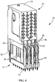
FIG. 5 is a front perspective view of an illustrative embodiment of a module of the backplane connector. -
FIG. 6 is a back perspective view of an illustrative embodiment of the module ofFIG. 5 . -
FIG. 7 is an exploded perspective view of the module ofFIG. 5 . -
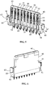
FIG. 8 is a front perspective view of a first alternate illustrative embodiment of a module of the backplane connector. -
FIG. 9 is a back perspective view of an illustrative embodiment of the module ofFIG. 8 . -
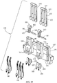
FIG. 10 is an exploded perspective view of the module ofFIG. 8 . -
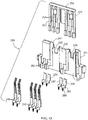
FIG. 11 is a front perspective view of an illustrative second embodiment of a module which can be used in a connector system. -
FIG. 12 is a back perspective view of the module ofFIG. 11 . -
FIG. 13 is an exploded perspective view of the module ofFIG. 11 . - An embodiment is directed to an electrical connector for use in an electrical connector system which controls cross-talk and signal radiation and optimizes impedance. The electrical connector includes a plurality of modules having mating ends and mounting ends. Each of the modules of the plurality of modules has a conductive first housing having. The first housing has at least one second housing recess provided in a first surface of the first housing. The first housing has ground contact receiving channels provided in the first surface of the first housing. At least one second housing is provided in the at least one second housing recess. The at least one second housing is made of insulative material and has signal contact receiving channels provided in a first surface of the at least one second housing. Signal contacts are positioned in the signal contact receiving channels of the at least one second housing. Ground contacts are positioned in the ground contact receiving channels of the first housing.
- An embodiment is directed to an electrical connector for use in an electrical connector system which controls cross-talk and signal radiation and optimizes impedance. The electrical connector includes a plurality of modules having mating ends and mounting ends. Each of the modules of the plurality of modules has a conductive first housing. The first housing has at least one second housing recess and ground contact receiving channels. At least one second housing is provided in the at least one second housing recess. The at least one second housing is made of insulative material and has signal contact receiving channels. Signal contacts are positioned in the signal contact receiving channels of the at least one second housing. The signal contacts are arranged in pairs to carry differential signals. Ground contacts are positioned in the ground contact receiving channels of the first housing. Respective ground contacts of the ground contacts are positioned adjacent to the at least one second housing and respective signal contacts of the signal contacts.
- An embodiment is directed to an electrical connector for use in an electrical connector system which controls cross-talk and signal radiation and optimizes impedance. The electrical connector includes a plurality of modules having mating ends and mounting ends. A first housing has at least one second housing recess provided in a first surface of the first housing. The first housing has ground shield receiving channels provided in a second surface of the first housing. The ground shield receiving channels are aligned with the at least one second housing recess. At least one second housing is provided in the at least one second housing recess. The at least one second housing is made of insulative material and has signal contact receiving channels. Signal contacts are positioned in the signal contact receiving channels of the at least one second housing. The signal contacts are arranged in pairs to carry differential signals. Ground shield plates are positioned in the ground shield receiving channels of the first housing to engage grounding contacts of a mating connector
-
FIGS. 1 through 7 illustrate anelectrical connector system 10 formed in accordance with an illustrative embodiment. Theelectrical connector system 10 includes abackplane connector 12 and adaughtercard connector 14 that are used to electrically connect a backplane circuit board (not shown) and a daughtercard circuit board (not shown). While theelectrical connector system 10 is described herein with reference tobackplane connectors 12 anddaughtercard connectors 14, it is realized that the subject matter herein may be utilized with different types of electrical connectors other than a backplane connector or a daughtercard connector. Thebackplane connector 12 and thedaughtercard connector 14 are merely illustrative embodiments of anelectrical connector system 10 that interconnects a particular type of circuit board, namely a backplane circuit board, with a daughtercard circuit board. - In the illustrative embodiment shown, the
daughtercard connector 14 constitutes a right angle connector wherein amating interface 16 andmounting interface 18 of thedaughtercard connector 14 are oriented perpendicular to one another. Thedaughtercard connector 14 is mounted to the daughtercard circuit board at the mountinginterface 18. Other orientations of theinterfaces - As shown in
FIGS. 1 ,2 and4 , thedaughtercard connector 14 includes ahousing 24, made of one or more components, holding a plurality ofcircuit boards 26 therein. Thecircuit boards 26 have pairs 28 of individual signal pathways or traces (not shown) that extend between themating interface 16 and the mountinginterface 18. The signal traces have signalconductive pads 32 provided proximate themating interface 16. The signal traces are configured to be mated with and electrically connected to thesignal contacts 48 of thebackplane connector 12. Thecircuit boards 26 have individual ground pathways or traces that extend between themating interface 16 and the mountinginterface 18. The ground traces (not shown) have groundconductive pads 36 provided proximate themating interface 16. The ground traces are configured to be mated with, and electrically connected to, theground contacts 50 or the shield or ground plates 52 of thebackplane connector 12. Thecircuit boards 26 also have ground pathways or traces 35 on opposites sides of thecircuit boards 26 from the ground traces. The ground traces 35 extend between themating interface 16 and the mountinginterface 18. In alternative embodiments, thecircuit boards 26 may be contact modules, the signal traces may be mating signal contacts and the ground traces may be ground contacts. - In the illustrated embodiment, the
backplane connector 12 constitutes a header connector mounted to the backplane circuit board. Thebackplane connector 12 is mated to thedaughtercard connector 14. When mated, the daughtercard circuit board is oriented generally perpendicular with respect to the backplane circuit board. - The
backplane connector 12 includes amating end 46 and a mountingend 42 that are oriented generally parallel to one another. Thebackplane connector 12 is mounted to the backplane circuit board at the mountingend 42. - The
backplane connector 12 includes ahousing 38 which includes a plurality ofmodules 40. Each of themodules 40 has amating end 46 , also referred to herein as afront end 46 , that is positioned in arecess 44 of thedaughtercard connector 14 during mating. Each of themodules 40 has a mountingend 42, also referred to herein as arear end 42, which is mounted to the backplane circuit board. Each of themodules 40 holds a plurality ofindividual signal contacts 48 that extend between themating end 46 and the mountingend 42. In an exemplary embodiment, thesignal contacts 48 are arranged in pairs carrying differential signals. Each of themodules 40 also holds a plurality ofground contacts 50 that extend between themating end 46 and the mountingend 42. - As shown in
FIGS. 5 through 7 , eachmodule 40 has a conductivefirst housing 41 and at least onesecond housing 43. In the illustrative embodiment shown, threesecond housings 43 are provided, but other numbers and configurations of thesecond housings 43 may be provided. - Each of the conductive
first housings 41 has afirst surface 45 and an oppositely facingsecond surface 47. At least one secondhousing receiving recess 49 extends from thefirst surface 45 toward thesecond surface 47. Thefirst housing 41 is an insulative member made of an insulative material with aconductive coating 51 applied to the outer surfaces of thefirst housing 41. Theconductive coating 51 may be applied by known methods or processes, including, but not limited to, an electroless process, an electroplating process or a physical vapor deposition process. Theconductive coating 51 allows thefirst housing 41 to act as a shield, as will be more fully described, while allowing themodules 40 and thebackplane connector 12 to mate with existingdaughtercard connectors 14. As thefirst housing 41 is made from an insulative materials, such as, but not limited to, plastic, the shape of thefirst housing 41 can be molded or manufactured in a shape which optimizes the impedance characteristics of thefirst housing 41 when theconductive coating 51 is applied. - The conductive
first housings 41 of themodules 40 include a plurality of ground cavities orchannels 60 extending between themating end 46 and the mountingend 42 of thefirst surface 45. Theground channels 60 extend from thefirst surface 45 toward thesecond surface 47 along the mating axes and receive theground contacts 50. When thebackplane connector 12 anddaughtercard connector 14 are mated, groundconductive pads 36 of the ground traces of thedaughtercard connector 14 are also received in the ground channels 6. Any number ofground channels 60 may be provided. Theground channels 60 may be provided at any locations within themodules 40 and thehousing 38. In an exemplary embodiment, theground channels 60 are generally positioned adjacent to and/or between the second housing receiving recesses 49. - The
second housings 43 have afirst surface 53 and an oppositely facingsecond surface 55. Thesecond housings 43 are insulative members made of an insulative material. Thesecond housings 43 may be separate components which are assembled to thefirst housings 41 using known methods, such as, but not limited to, adhesion, interference fit, overmolding and/or mounting projections. - The
second housings 43 of themodules 40 include a plurality of signal cavities orchannels 54 extending between themating end 46 and the mountingend 42 of thefirst surface 53. Thesignal channels 54 extend along the mating axes and receive thesignal contacts 48. When thebackplane connector 12 anddaughtercard connector 14 are mated, the signalconductive pads 32 of the mating signal traces of thedaughtercard connector 14 are also received in thesignal channels 60. In the illustrative embodiment shown, two signal cavities orchannels 54 are provided in each of thesecond housings 43, however, other numbers of signal cavities orchannels 54 may be provided. - In the illustrative embodiment shown in
FIG. 1 and2 , thehousing 38 of thebackplane connector 12 has fourmodules 40 which are positioned adjacent to each other. However, other number of modules may be used. Circuitboard receiving slots 62 are provided betweenadjacent modules 40. The circuitboard receiving slots 62 are positioned adjacent mating connector receiving sections 64 of themodules 40. Each circuitboard receiving slot 62 extends from themating end 46 of the module toward the mountingend 42. - Each of the
first housings 41 of themodules 40 has abase section 66 which extends from the mountingend 42 toward themating end 46 . Thebase section 66 hasend sections 67 which extend beyond the connector receiving sections 64, as shown inFIGS. 5 and 6 . Each of theend sections 67 has aclip receiving slot 68 which extends from a top surface 65 of theend section 67 toward the mountingend 42. - When the
modules 40 are properly assembled, as shown inFIGS. 1 through 3 , clips 69 are inserted into theclip receiving slots 68 to properly position and retain themodules 40 in position relative to each other. - Referring to
FIGS. 5 and7 , thesignal channels 54 andground channels 60 are shown. As previously described, thesignal channels 54 are configured to receive thesignal contacts 48 therein. As shown inFIG. 7 , eachsignal contact 48 has a matingcontact receiving section 71, a securingsection 72 and circuitboard mounting section 73. In the illustrative embodiment shown, thecontact receiving section 71 includes tworesilient arms 74 with lead-inportions 75 andengagement portions 76. Theresilient arms 74 are configured to press against the signalconductive pads 32 of the signal traces when thedaughter card connector 14 is mated to thebackplane connector 12. The circuitboard mounting section 73 has acompliant portion 78, such as an eye of the needle pin, although other configurations may be used. Each of the circuitboard mounting section 73 has a longitudinal axis which is offset from the longitudinal axis of the securingsection 72 and the matingcontact receiving section 71. In various illustrative embodiments, thesignal contacts 48 of onemodule 40 have the circuitboard mounting section 73 offset to the right, while thesignal contacts 48 of anothermodule 40 have the circuitboard mounting section 73 offset to the left. As the mountingsection 73 of thesignal contacts 48 in onemodule 40 are offset from the mountingsection 73 of thesignal contacts 48 in anadjacent module 40, the cross-talk is reduced in the footprint of thebackplane connector 12, as the staggered pattern is configured for cancellation. - As previously described, the
ground channels 60 are configured to receive theground contacts 50 therein. Eachground contact 50 has acontact section 80, a securingsection 81 and circuitboard mounting section 82. In the illustrative embodiment shown, thecontact section 80 includes tworesilient arms 83 with lead-inportions 84 andengagement portions 85. Theresilient arms 83 are configured to press against the groundconductive pads 36 of the ground traces when thedaughter card connector 14 is mated to thebackplane connector 12. - The circuit
board mounting section 82 has acompliant portion 87, such as an eye of the needle pin, although other configurations may be used. Each of the circuitboard mounting section 82 has a longitudinal axis which is offset from the longitudinal axis of the securingsection 81 and thecontact section 80. In various illustrative embodiments, theground contacts 50 of onemodule 40 have the circuitboard mounting section 82 offset to the right, while theground contacts 50 of anothermodule 40 have the circuitboard mounting section 82 offset to the left. - With the
housing 38 properly assembled, theground contacts 50 and the conductivefirst housings 41 with theconductive coatings 51 extend about the periphery of the pairs ofsignal contacts 48 and surround the pairs ofsignal contacts 48 to provide electrical shielding for the pairs ofsignal contacts 48.Respective ground contacts 50 are positioned adjacent to the at least onesecond housing 43 andrespective signal contacts 48. In an exemplary embodiment, entire, 360 degree shielding is provided by theground contacts 50 and the conductivefirst housings 41 along the length of thesignal contacts 48. Theground contacts 50 and the conductivefirst housings 51 surround portions of the mating signal traces when theconnectors ground contacts 50 and the conductivefirst housings 41 provide shielding along the entire mating interface with the mating signal traces. Theground contacts 50 and the conductivefirst housings 41 may control electrical characteristics throughout thehousing 38, such as by controlling cross-talk, signal radiation, impedance or other electrical characteristics. - With the
daughtercard connector 14 properly mated to thebackplane connector 12, thecircuit boards 26 of thedaughter card connector 14 are positioned in the circuitboard receiving slots 62. In this position, thesignal contacts 48 of themodules 40 physically and electrically engage the signalconductive pads 32 of the signal traces of thecircuit boards 26. Theground contacts 50 of themodules 40 are also placed in physical and electrical engagement with the groundconductive pads 36 of the ground traces of thecircuit boards 26. In addition, the conductivefirst housings 41 physically and electrically engage theground contacts 50. - The
ground contacts 50 and the conductivefirst housings 41 provide shielding for thesignal contacts 48 and the portions of the signalconductive pads 32 of the signal traces of thecircuit boards 26 which are positioned in the circuitboard receiving slots 62 of themodules 40 of thehousing 38 of thebackplane connector 12. - Referring to
FIGS. 8 through 10 , a first alternate illustrative embodiment of amodule 140 is shown. Eachmodule 140 has a conductivefirst housing 141 and at least onesecond housing 143. In the illustrative embodiment shown, twosecond housings 143 are provided, but other numbers and configurations of thesecond housings 143 may be provided. - As shown in
FIG. 10 , each of the conductivefirst housings 141 has afirst surface 145 and an oppositely facingsecond surface 147. At least one secondhousing receiving recess 149 extends from thefirst surface 145 toward thesecond surface 147. Thefirst housing 141 is an insulative member made of an insulative material with aconductive coating 151 applied to the outer surfaces of thefirst housing 141. Theconductive coating 151 may be applied by known methods or processes, including, but not limited to, an electroless process, an electroplating process or a physical vapor deposition process. Theconductive coating 151 allows thefirst housing 141 to act as a shield, as will be more fully described, while allowing themodules 140 and thebackplane connector 12 to mate with existingdaughtercard connectors 14. As thefirst housing 141 is made from an insulative materials, such as, but not limited to, plastic, the shape of thefirst housing 141 can be molded or manufactured in a shape which optimizes the impedance characteristics of thefirst housing 141 when theconductive coating 151 is applied. - The conductive
first housings 141 of themodules 140 include a plurality of first ground cavities orchannels 160 and second ground cavities orchannels 161 extending from thefirst surface 145 toward thesecond surface 147. When thebackplane connector 12 anddaughtercard connector 14 are mated, groundconductive pads 36 of the ground traces of thedaughtercard connector 14 are also received in theground channels 160. Any number offirst ground channels 160 andsecond ground channels 161 may be provided. Theground channels 160 andsecond ground channels 161 may be provided at any locations within themodules 140. In an exemplary embodiment, theground channels 160 andsecond ground channels 161 are generally positioned adjacent to and/or between the second housing receiving recesses 149. - The conductive
first housings 141 of themodules 140 also include a plurality of third ground cavities orchannels 163 extending from thesecond surface 147 toward thefirst surface 145. The third ground cavities orchannels 163 intersect with the first cavities orchannels 160 proximate themating end 146 . - The
second housings 143 have afirst surface 153 and an oppositely facingsecond surface 155. Thesecond housings 143 are insulative members made of an insulative material. Thesecond housings 143 may be separate components which are assembled to thefirst housings 141 using known methods, such as, but not limited to, adhesion, interference fit, overmolding and/or mounting projections. - The
second housings 143 of themodules 140 include a plurality of signal cavities orchannels 154 extending between themating end 146 and the mountingend 142. Thesignal channels 154 extend along the mating axes and receive thesignal contacts 148. When thebackplane connector 12 anddaughtercard connector 14 are mated, the signalconductive pads 32 of the mating signal traces of thedaughtercard connector 14 are also received in thesignal channels 154. In the illustrative embodiment shown, two signal cavities orchannels 154 are provided in each of thesecond housings 143, however, other numbers of signal cavities orchannels 154 may be provided. - As previously described, the
signal channels 154 are configured to receive thesignal contacts 148. Thesignal contacts 148 are similar to thesignal contacts 48 previously described. - The
ground channels 160 andground channels 163 are configured to receive theground contacts 150 therein. Eachground contact 150 has afirst contact section 180, a bent or securingsection 181 and asecond contact section 182. In the illustrative embodiment shown, thefirst contact section 180 has tworesilient arms 183. Theresilient arms 183 are configured to press against the groundconductive pads 36 of the ground traces when thedaughter card connector 14 is mated to thebackplane connector 12. - The
bent section 181 extends between thefirst contact section 180 and thesecond contact section 182. Thebent section 181 also extends between the first ground cavities orchannels 160 on thefirst surface 145 and the third ground cavities orchannels 163 on thesecond surface 147. Thesecond contact sections 182 haveprojection 187 which extend beyond thesecond surface 147 to physically and electrically engage the ground traces 35 of thecircuit boards 26. - The
ground channels 161 are configured to receive theground contacts 159 therein. Eachground contact 159 has amodule engagement section 187 and a circuitboard mounting section 188. The circuitboard mounting section 188 has acompliant portion 189, such as an eye of the needle pin, although other configurations may be used. - With the
housing 38 properly assembled, theground contacts 150 and the conductivefirst housings 141 with theconductive coatings 151 extend about the periphery of the pairs ofsignal contacts 148 and surround the pairs ofsignal contacts 148 to provide electrical shielding for the pairs ofsignal contacts 148.Respective ground contacts 150 are positioned adjacent to the at least onesecond housing 143 andrespective signal contacts 148. In an exemplary embodiment, entire, 360 degree shielding is provided by theground contacts 150 and the conductivefirst housings 141 along the length of thesignal contacts 148. Theground contacts 150 and the conductivefirst housings 151 surround portions of the mating signal traces when theconnectors ground contacts 150 and the conductivefirst housings 141 provide shielding along the entire mating interface with the mating signal traces. Theground contacts 150 and the conductivefirst housings 141 may control electrical characteristics throughout thehousing 38, such as by controlling cross-talk, signal radiation, impedance or other electrical characteristics. - Referring to
FIGS. 11 through 13 , a second alternate illustrative embodiment of amodule 240 is shown. Eachmodule 240 has a conductivefirst housing 241 and at least onesecond housing 243. - The conductive
first housing 241 has afirst surface 245 and an oppositely facingsecond surface 247. At least one secondhousing receiving recess 249 extends from thefirst surface 245 toward thesecond surface 247. Thefirst housing 241 is an insulative member made of an insulative material with aconductive coating 251 applied to the outer surfaces of thefirst housing 241. Theconductive coating 251 may be applied by known methods or processes, including, but not limited to, an electroless process, an electroplating process or a physical vapor deposition process. Theconductive coating 251 allows thefirst housing 241 to act as a shield, as will be more fully described, while allowing themodules 240 and thebackplane connector 12 to mate with existingdaughtercard connectors 14. As thefirst housing 241 is made from an insulative materials, such as, but not limited to, plastic, the shape of thefirst housing 241 can be molded or manufactured in a shape which optimizes the impedance characteristics of thefirst housing 241 when theconductive coating 251 is applied. - The conductive
first housings 241 of themodules 240 include a plurality of ground shield receiving channels orcavities 260 extending from thesecond surface 247 toward thefirst surface 245. The groundshield receiving channels 260 are provided in alignment with the second housing receiving recesses 249. - The
second housing 243 has afirst surface 253 and an oppositely facingsecond surface 255. Thesecond housing 243 is made of an insulative material. In other embodiments, thesecond housing 243 may have separate components which are assembled to thefirst housings 241 using known methods, such as, but not limited to, adhesion, interference fit, overmolding and/or mounting projections. - The
second housing 243 of themodules 240 includes a plurality of signal cavities orchannels 254 extending between themating end 246 and the mountingend 242. Thesignal channels 254 extend along the mating axes and receive thesignal contacts 248. When thebackplane connector 12 anddaughtercard connector 14 are mated, the signalconductive pads 32 of the mating signal traces of thedaughtercard connector 14 are also received in thesignal channels 254. In the illustrative embodiment shown, two pairs of signal cavities orchannels 254 are provided in thesecond housing 243, however, other numbers of signal cavities orchannels 254 may be provided. - As previously described, the
signal channels 254 are configured to receive thesignal contacts 248. Thesignal contacts 248 are similar to thesignal contacts 48 previously described. - The ground
shield receiving channels 260 are configured to receive shield orground plates 250 therein. In the illustrative embodiment shown, thesecond housing 243 is overmolded over the shield orground plates 250. The shield orground plates 250 are positioned to mechanically and electrically engage the ground traces 35 to provide proper shielding to control cross-talk, signal radiation, impedance or other electrical characteristics. - With the
housing 38 properly assembled, the shield orground plates 250 and the conductivefirst housings 241 with theconductive coatings 251 extend about the periphery of the pairs ofsignal contacts 248 and surround the pairs ofsignal contacts 248 to provide electrical shielding for the pairs ofsignal contacts 248. In an exemplary embodiment, entire, 360 degree shielding is provided by the shield orground plates 250 and the conductivefirst housings 241 along the length of thesignal contacts 248. The shield orground plates 250 and the conductivefirst housings 251 surround portions of the mating signal traces when theconnectors ground plates 250 and the conductivefirst housings 241 provide shielding along the entire mating interface with the mating signal traces. The shield orground plates 250 and the conductivefirst housings 241 may control electrical characteristics throughout thehousing 38, such as by controlling cross-talk, signal radiation, impedance or other electrical characteristics.
Claims (10)
- An electrical connector (12) for use in an electrical connector system (10) which controls cross-talk, signal radiation and impedance, the electrical connector (12) comprising:a plurality of modules (40, 140), the modules (40, 140) having mating ends (46, 146) and mounting ends (42,142);each of the modules (40, 140) of the plurality of modules (40, 140) comprising:a conductive first housing (41, 141), the first housing (41, 141) having at least one second housing recess (49, 149) provided in a first surface (45, 145) of the first housing (41, 141), the first housing (41, 141) having ground contact receiving channels (60, 160) provided in the first surface (45, 145) of the first housing (41, 141);at least one second housing (43, 143) provided in the at least one second housing recess (49, 149), the at least one second housing (43, 143) being made of insulative material, the at least one second housing (43, 143) having signal contact receiving channels (54, 154) provided in a first surface (53, 153) of the at least one second housing (43, 143);signal contacts (48, 148) positioned in the signal contact receiving channels (54, 154) of the at least one second housing (43, 143);ground contacts (50, 150) positioned in the ground contact receiving channels (60, 160) of the first housing (41, 141).
- The electrical connector (12) as recited in claim 1, wherein each of the at least one second housing (43, 143) has a pair of said signal contacts (48, 148) to carry differential signals.
- The electrical connector (12) as recited in claim 1 or 2, wherein respective ground contacts (50, 150) of the ground contacts (50, 150) are positioned adjacent to the at least one second housing (43, 143) and respective signal contacts (48, 148) of the signal contacts (48, 148).
- The electrical connector (12) as recited in any preceding claim, wherein the first housing (41, 141) is an insulative member with a conductive coating (51, 151) applied thereto.
- The electrical connector (12) as recited in claim 4, wherein the conductive coating (51, 151) is applied by a physical vapor deposition process.
- The electrical connector (12) as recited in claim 4, wherein the conductive coating (51, 151) is applied by a plating process.
- The electrical connector (12) as recited in claim 1, wherein the first housing (141) has ground contact receiving channels (163) provided in a second surface (147) of the first housing (141).
- The electrical connector (12) as recited in claim 7, wherein respective ground contacts (150) of the ground contacts (150) extend from in the ground contact receiving channels (160) provided in the first surface (145) of the first housing (140) to the ground contact receiving channels (163) provided in the second surface (147) of the first housing (141).
- The electrical connector (12) as recited in claim 8, wherein the respective ground contacts (150) of the ground contacts (150) which extend from the ground contact receiving channels (160) provided in the first surface (145) of the first housing (141) to the ground contact receiving channels (163) provided in the second surface (147) of the first housing (141) have projections (187) which extend from the second surface (147) to engage grounding contacts (35) of a mating connector (14).
- The electrical connector (12) as recited in any preceding claim, wherein the at least one second housing (43, 143) is overmolded over the first housing (41, 141).
Applications Claiming Priority (1)
| Application Number | Priority Date | Filing Date | Title |
|---|---|---|---|
| US16/830,687 US10965062B1 (en) | 2020-03-26 | 2020-03-26 | Modular electrical connector with conductive coating to reduce crosstalk |
Publications (2)
| Publication Number | Publication Date |
|---|---|
| EP3886268A1 true EP3886268A1 (en) | 2021-09-29 |
| EP3886268B1 EP3886268B1 (en) | 2024-12-18 |
Family
ID=75143462
Family Applications (1)
| Application Number | Title | Priority Date | Filing Date |
|---|---|---|---|
| EP21163857.2A Active EP3886268B1 (en) | 2020-03-26 | 2021-03-22 | Modular electrical connector with conductive coating to reduce cross-talk |
Country Status (2)
| Country | Link |
|---|---|
| US (1) | US10965062B1 (en) |
| EP (1) | EP3886268B1 (en) |
Families Citing this family (3)
| Publication number | Priority date | Publication date | Assignee | Title |
|---|---|---|---|---|
| CN115347423B (en) * | 2021-05-13 | 2025-09-16 | 泰科电子(上海)有限公司 | Electric connector assembly |
| CN216055251U (en) * | 2021-08-03 | 2022-03-15 | 东莞立讯技术有限公司 | Connector assembly |
| TWI824615B (en) * | 2022-07-11 | 2023-12-01 | 貿聯國際股份有限公司 | Signal connector |
Citations (3)
| Publication number | Priority date | Publication date | Assignee | Title |
|---|---|---|---|---|
| US6663429B1 (en) * | 2002-08-29 | 2003-12-16 | Hon Hai Precision Ind. Co., Ltd. | Method for manufacturing high density electrical connector assembly |
| US20120214344A1 (en) * | 2011-02-18 | 2012-08-23 | Cohen Thomas S | High speed, high density electrical connector |
| US20190296469A1 (en) * | 2018-03-22 | 2019-09-26 | Amphenol Corporation | High density electrical connector |
Family Cites Families (29)
| Publication number | Priority date | Publication date | Assignee | Title |
|---|---|---|---|---|
| US6663442B1 (en) | 2000-01-27 | 2003-12-16 | Tyco Electronics Corporation | High speed interconnect using printed circuit board with plated bores |
| US6267604B1 (en) | 2000-02-03 | 2001-07-31 | Tyco Electronics Corporation | Electrical connector including a housing that holds parallel circuit boards |
| US6171115B1 (en) | 2000-02-03 | 2001-01-09 | Tyco Electronics Corporation | Electrical connector having circuit boards and keying for different types of circuit boards |
| US6824391B2 (en) | 2000-02-03 | 2004-11-30 | Tyco Electronics Corporation | Electrical connector having customizable circuit board wafers |
| AU2001264942A1 (en) | 2000-05-25 | 2001-12-03 | Tyco Electronics Corporation | Electrical connector having contacts isolated by shields |
| US6540522B2 (en) | 2001-04-26 | 2003-04-01 | Tyco Electronics Corporation | Electrical connector assembly for orthogonally mating circuit boards |
| US6384341B1 (en) | 2001-04-30 | 2002-05-07 | Tyco Electronics Corporation | Differential connector footprint for a multi-layer circuit board |
| US6488549B1 (en) | 2001-06-06 | 2002-12-03 | Tyco Electronics Corporation | Electrical connector assembly with separate arcing zones |
| US6582250B2 (en) | 2001-11-20 | 2003-06-24 | Tyco Electronics Corporation | Connector module organizer |
| US6663426B2 (en) | 2002-01-09 | 2003-12-16 | Tyco Electronics Corporation | Floating interface for electrical connector |
| US6655966B2 (en) | 2002-03-19 | 2003-12-02 | Tyco Electronics Corporation | Modular connector with grounding interconnect |
| US6705895B2 (en) | 2002-04-25 | 2004-03-16 | Tyco Electronics Corporation | Orthogonal interface for connecting circuit boards carrying differential pairs |
| US6638110B1 (en) * | 2002-05-22 | 2003-10-28 | Hon Hai Precision Ind. Co., Ltd. | High density electrical connector |
| US6890214B2 (en) | 2002-08-21 | 2005-05-10 | Tyco Electronics Corporation | Multi-sequenced contacts from single lead frame |
| US6808399B2 (en) | 2002-12-02 | 2004-10-26 | Tyco Electronics Corporation | Electrical connector with wafers having split ground planes |
| US6811414B1 (en) | 2003-05-16 | 2004-11-02 | Tyco Electronics Corporation | Electrical connector module with multiple card edge sections |
| US6811440B1 (en) | 2003-08-29 | 2004-11-02 | Tyco Electronics Corporation | Power connector |
| US6964583B2 (en) | 2004-02-13 | 2005-11-15 | Tyco Electronics Corporation | Connector having low frequency noise reducing ground |
| US6932649B1 (en) | 2004-03-19 | 2005-08-23 | Tyco Electronics Corporation | Active wafer for improved gigabit signal recovery, in a serial point-to-point architecture |
| US6997736B2 (en) | 2004-03-26 | 2006-02-14 | Tyco Electronics Corporation | Guide receptacle with tandem mounting features |
| US6945810B1 (en) | 2004-04-28 | 2005-09-20 | Tyco Electronics Corporation | Double ended guide pin for keying on both sides of a circuit board |
| US7044794B2 (en) | 2004-07-14 | 2006-05-16 | Tyco Electronics Corporation | Electrical connector with ESD protection |
| US7175445B2 (en) | 2004-08-31 | 2007-02-13 | Tyco Electronics Corporation | Electrical connector power wafers |
| US7789676B2 (en) * | 2008-08-19 | 2010-09-07 | Tyco Electronics Corporation | Electrical connector with electrically shielded terminals |
| JP5684710B2 (en) * | 2008-09-23 | 2015-03-18 | アンフェノール コーポレイション | High density electrical connector |
| US8840431B2 (en) | 2012-10-26 | 2014-09-23 | Tyco Electronics Corporation | Electrical connector systems |
| CN107112696B (en) * | 2014-11-12 | 2020-06-09 | 安费诺有限公司 | Very high speed, high density electrical interconnect system with impedance control in the mating area |
| US10535971B2 (en) | 2017-10-12 | 2020-01-14 | Te Connectivity Corporation | Electrical connector |
| CN110994230B (en) * | 2018-12-28 | 2021-06-18 | 富鼎精密工业(郑州)有限公司 | electrical connector |
-
2020
- 2020-03-26 US US16/830,687 patent/US10965062B1/en active Active
-
2021
- 2021-03-22 EP EP21163857.2A patent/EP3886268B1/en active Active
Patent Citations (3)
| Publication number | Priority date | Publication date | Assignee | Title |
|---|---|---|---|---|
| US6663429B1 (en) * | 2002-08-29 | 2003-12-16 | Hon Hai Precision Ind. Co., Ltd. | Method for manufacturing high density electrical connector assembly |
| US20120214344A1 (en) * | 2011-02-18 | 2012-08-23 | Cohen Thomas S | High speed, high density electrical connector |
| US20190296469A1 (en) * | 2018-03-22 | 2019-09-26 | Amphenol Corporation | High density electrical connector |
Also Published As
| Publication number | Publication date |
|---|---|
| US10965062B1 (en) | 2021-03-30 |
| EP3886268B1 (en) | 2024-12-18 |
Similar Documents
| Publication | Publication Date | Title |
|---|---|---|
| EP3886261B1 (en) | Modular electrical connector with reduced cross-talk | |
| EP3890120B1 (en) | Modular electrical connector with additional grounding | |
| US6544072B2 (en) | Electrical connector with metallized polymeric housing | |
| EP0460976B1 (en) | Connectors with ground structure | |
| US7744385B2 (en) | High speed cable termination electrical connector assembly | |
| US5135405A (en) | Connectors with ground structure | |
| EP2209170B1 (en) | Orthogonal connector system | |
| US5228864A (en) | Connectors with ground structure | |
| US5133679A (en) | Connectors with ground structure | |
| CN103378516B (en) | Electric connector system with impedance control | |
| US7824187B1 (en) | High density connector | |
| CN102570116B (en) | For the interface contacts of electric connector | |
| EP3890119B1 (en) | Shield component for use with modular electrical connector to reduce cross-talk | |
| EP3886268B1 (en) | Modular electrical connector with conductive coating to reduce cross-talk | |
| US9531129B2 (en) | Electrical connector and connector system having bussed ground conductors | |
| US10868393B2 (en) | Electrical connector assembly for a communication system | |
| TWI907483B (en) | Contact module for a header assembly | |
| EP3886269B1 (en) | Modular printed circuit board wafer connector with reduced cross-talk | |
| EP4362241A1 (en) | Ground shields positioned between columns of contacts | |
| EP3886270B1 (en) | Modular connector with printed circuit board wafer to reduce cross-talk | |
| EP4362240B1 (en) | Contact and shield configuration for ground current optimization | |
| US4772211A (en) | Multi-plane interconnection system | |
| US12438315B2 (en) | Electrical connector with improved terminal groups and connector assembly having the same | |
| EP4681293A1 (en) | Ground shield contact member |
Legal Events
| Date | Code | Title | Description |
|---|---|---|---|
| PUAI | Public reference made under article 153(3) epc to a published international application that has entered the european phase |
Free format text: ORIGINAL CODE: 0009012 |
|
| STAA | Information on the status of an ep patent application or granted ep patent |
Free format text: STATUS: THE APPLICATION HAS BEEN PUBLISHED |
|
| AK | Designated contracting states |
Kind code of ref document: A1 Designated state(s): AL AT BE BG CH CY CZ DE DK EE ES FI FR GB GR HR HU IE IS IT LI LT LU LV MC MK MT NL NO PL PT RO RS SE SI SK SM TR |
|
| STAA | Information on the status of an ep patent application or granted ep patent |
Free format text: STATUS: REQUEST FOR EXAMINATION WAS MADE |
|
| 17P | Request for examination filed |
Effective date: 20220321 |
|
| RBV | Designated contracting states (corrected) |
Designated state(s): AL AT BE BG CH CY CZ DE DK EE ES FI FR GB GR HR HU IE IS IT LI LT LU LV MC MK MT NL NO PL PT RO RS SE SI SK SM TR |
|
| RAP1 | Party data changed (applicant data changed or rights of an application transferred) |
Owner name: TE CONNECTIVITY SOLUTIONS GMBH |
|
| STAA | Information on the status of an ep patent application or granted ep patent |
Free format text: STATUS: EXAMINATION IS IN PROGRESS |
|
| 17Q | First examination report despatched |
Effective date: 20230927 |
|
| GRAP | Despatch of communication of intention to grant a patent |
Free format text: ORIGINAL CODE: EPIDOSNIGR1 |
|
| STAA | Information on the status of an ep patent application or granted ep patent |
Free format text: STATUS: GRANT OF PATENT IS INTENDED |
|
| RIC1 | Information provided on ipc code assigned before grant |
Ipc: H01R 13/6599 20110101ALN20240726BHEP Ipc: H01R 13/502 20060101ALN20240726BHEP Ipc: H01R 12/73 20110101ALN20240726BHEP Ipc: H01R 24/60 20110101ALN20240726BHEP Ipc: H05K 1/02 20060101ALN20240726BHEP Ipc: H01R 13/6473 20110101ALN20240726BHEP Ipc: H01R 12/71 20110101ALN20240726BHEP Ipc: H05K 1/14 20060101ALI20240726BHEP Ipc: H01R 13/6587 20110101ALI20240726BHEP Ipc: H01R 13/6471 20110101AFI20240726BHEP |
|
| INTG | Intention to grant announced |
Effective date: 20240823 |
|
| GRAS | Grant fee paid |
Free format text: ORIGINAL CODE: EPIDOSNIGR3 |
|
| GRAA | (expected) grant |
Free format text: ORIGINAL CODE: 0009210 |
|
| STAA | Information on the status of an ep patent application or granted ep patent |
Free format text: STATUS: THE PATENT HAS BEEN GRANTED |
|
| AK | Designated contracting states |
Kind code of ref document: B1 Designated state(s): AL AT BE BG CH CY CZ DE DK EE ES FI FR GB GR HR HU IE IS IT LI LT LU LV MC MK MT NL NO PL PT RO RS SE SI SK SM TR |
|
| REG | Reference to a national code |
Ref country code: CH Ref legal event code: EP |
|
| REG | Reference to a national code |
Ref country code: DE Ref legal event code: R096 Ref document number: 602021023422 Country of ref document: DE |
|
| REG | Reference to a national code |
Ref country code: IE Ref legal event code: FG4D |
|
| REG | Reference to a national code |
Ref country code: LT Ref legal event code: MG9D |
|
| PG25 | Lapsed in a contracting state [announced via postgrant information from national office to epo] |
Ref country code: HR Free format text: LAPSE BECAUSE OF FAILURE TO SUBMIT A TRANSLATION OF THE DESCRIPTION OR TO PAY THE FEE WITHIN THE PRESCRIBED TIME-LIMIT Effective date: 20241218 |
|
| PG25 | Lapsed in a contracting state [announced via postgrant information from national office to epo] |
Ref country code: FI Free format text: LAPSE BECAUSE OF FAILURE TO SUBMIT A TRANSLATION OF THE DESCRIPTION OR TO PAY THE FEE WITHIN THE PRESCRIBED TIME-LIMIT Effective date: 20241218 |
|
| PG25 | Lapsed in a contracting state [announced via postgrant information from national office to epo] |
Ref country code: BG Free format text: LAPSE BECAUSE OF FAILURE TO SUBMIT A TRANSLATION OF THE DESCRIPTION OR TO PAY THE FEE WITHIN THE PRESCRIBED TIME-LIMIT Effective date: 20241218 |
|
| PG25 | Lapsed in a contracting state [announced via postgrant information from national office to epo] |
Ref country code: NO Free format text: LAPSE BECAUSE OF FAILURE TO SUBMIT A TRANSLATION OF THE DESCRIPTION OR TO PAY THE FEE WITHIN THE PRESCRIBED TIME-LIMIT Effective date: 20250318 |
|
| REG | Reference to a national code |
Ref country code: NL Ref legal event code: MP Effective date: 20241218 |
|
| PG25 | Lapsed in a contracting state [announced via postgrant information from national office to epo] |
Ref country code: LV Free format text: LAPSE BECAUSE OF FAILURE TO SUBMIT A TRANSLATION OF THE DESCRIPTION OR TO PAY THE FEE WITHIN THE PRESCRIBED TIME-LIMIT Effective date: 20241218 Ref country code: GR Free format text: LAPSE BECAUSE OF FAILURE TO SUBMIT A TRANSLATION OF THE DESCRIPTION OR TO PAY THE FEE WITHIN THE PRESCRIBED TIME-LIMIT Effective date: 20250319 |
|
| PG25 | Lapsed in a contracting state [announced via postgrant information from national office to epo] |
Ref country code: RS Free format text: LAPSE BECAUSE OF FAILURE TO SUBMIT A TRANSLATION OF THE DESCRIPTION OR TO PAY THE FEE WITHIN THE PRESCRIBED TIME-LIMIT Effective date: 20250318 |
|
| PG25 | Lapsed in a contracting state [announced via postgrant information from national office to epo] |
Ref country code: NL Free format text: LAPSE BECAUSE OF FAILURE TO SUBMIT A TRANSLATION OF THE DESCRIPTION OR TO PAY THE FEE WITHIN THE PRESCRIBED TIME-LIMIT Effective date: 20241218 |
|
| REG | Reference to a national code |
Ref country code: AT Ref legal event code: MK05 Ref document number: 1753024 Country of ref document: AT Kind code of ref document: T Effective date: 20241218 |
|
| PG25 | Lapsed in a contracting state [announced via postgrant information from national office to epo] |
Ref country code: SM Free format text: LAPSE BECAUSE OF FAILURE TO SUBMIT A TRANSLATION OF THE DESCRIPTION OR TO PAY THE FEE WITHIN THE PRESCRIBED TIME-LIMIT Effective date: 20241218 |
|
| PG25 | Lapsed in a contracting state [announced via postgrant information from national office to epo] |
Ref country code: PL Free format text: LAPSE BECAUSE OF FAILURE TO SUBMIT A TRANSLATION OF THE DESCRIPTION OR TO PAY THE FEE WITHIN THE PRESCRIBED TIME-LIMIT Effective date: 20241218 |
|
| PG25 | Lapsed in a contracting state [announced via postgrant information from national office to epo] |
Ref country code: ES Free format text: LAPSE BECAUSE OF FAILURE TO SUBMIT A TRANSLATION OF THE DESCRIPTION OR TO PAY THE FEE WITHIN THE PRESCRIBED TIME-LIMIT Effective date: 20241218 |
|
| PG25 | Lapsed in a contracting state [announced via postgrant information from national office to epo] |
Ref country code: IS Free format text: LAPSE BECAUSE OF FAILURE TO SUBMIT A TRANSLATION OF THE DESCRIPTION OR TO PAY THE FEE WITHIN THE PRESCRIBED TIME-LIMIT Effective date: 20250418 |
|
| PG25 | Lapsed in a contracting state [announced via postgrant information from national office to epo] |
Ref country code: PT Free format text: LAPSE BECAUSE OF FAILURE TO SUBMIT A TRANSLATION OF THE DESCRIPTION OR TO PAY THE FEE WITHIN THE PRESCRIBED TIME-LIMIT Effective date: 20250421 |
|
| PG25 | Lapsed in a contracting state [announced via postgrant information from national office to epo] |
Ref country code: EE Free format text: LAPSE BECAUSE OF FAILURE TO SUBMIT A TRANSLATION OF THE DESCRIPTION OR TO PAY THE FEE WITHIN THE PRESCRIBED TIME-LIMIT Effective date: 20241218 |
|
| PG25 | Lapsed in a contracting state [announced via postgrant information from national office to epo] |
Ref country code: RO Free format text: LAPSE BECAUSE OF FAILURE TO SUBMIT A TRANSLATION OF THE DESCRIPTION OR TO PAY THE FEE WITHIN THE PRESCRIBED TIME-LIMIT Effective date: 20241218 Ref country code: AT Free format text: LAPSE BECAUSE OF FAILURE TO SUBMIT A TRANSLATION OF THE DESCRIPTION OR TO PAY THE FEE WITHIN THE PRESCRIBED TIME-LIMIT Effective date: 20241218 |
|
| PG25 | Lapsed in a contracting state [announced via postgrant information from national office to epo] |
Ref country code: SK Free format text: LAPSE BECAUSE OF FAILURE TO SUBMIT A TRANSLATION OF THE DESCRIPTION OR TO PAY THE FEE WITHIN THE PRESCRIBED TIME-LIMIT Effective date: 20241218 |
|
| PG25 | Lapsed in a contracting state [announced via postgrant information from national office to epo] |
Ref country code: CZ Free format text: LAPSE BECAUSE OF FAILURE TO SUBMIT A TRANSLATION OF THE DESCRIPTION OR TO PAY THE FEE WITHIN THE PRESCRIBED TIME-LIMIT Effective date: 20241218 |
|
| PG25 | Lapsed in a contracting state [announced via postgrant information from national office to epo] |
Ref country code: IT Free format text: LAPSE BECAUSE OF FAILURE TO SUBMIT A TRANSLATION OF THE DESCRIPTION OR TO PAY THE FEE WITHIN THE PRESCRIBED TIME-LIMIT Effective date: 20241218 |
|
| PG25 | Lapsed in a contracting state [announced via postgrant information from national office to epo] |
Ref country code: SE Free format text: LAPSE BECAUSE OF FAILURE TO SUBMIT A TRANSLATION OF THE DESCRIPTION OR TO PAY THE FEE WITHIN THE PRESCRIBED TIME-LIMIT Effective date: 20241218 |
|
| REG | Reference to a national code |
Ref country code: DE Ref legal event code: R097 Ref document number: 602021023422 Country of ref document: DE |
|
| PG25 | Lapsed in a contracting state [announced via postgrant information from national office to epo] |
Ref country code: DK Free format text: LAPSE BECAUSE OF FAILURE TO SUBMIT A TRANSLATION OF THE DESCRIPTION OR TO PAY THE FEE WITHIN THE PRESCRIBED TIME-LIMIT Effective date: 20241218 |
|
| PG25 | Lapsed in a contracting state [announced via postgrant information from national office to epo] |
Ref country code: MC Free format text: LAPSE BECAUSE OF FAILURE TO SUBMIT A TRANSLATION OF THE DESCRIPTION OR TO PAY THE FEE WITHIN THE PRESCRIBED TIME-LIMIT Effective date: 20241218 |
|
| REG | Reference to a national code |
Ref country code: CH Ref legal event code: H13 Free format text: ST27 STATUS EVENT CODE: U-0-0-H10-H13 (AS PROVIDED BY THE NATIONAL OFFICE) Effective date: 20251023 |
|
| PLBE | No opposition filed within time limit |
Free format text: ORIGINAL CODE: 0009261 |
|
| STAA | Information on the status of an ep patent application or granted ep patent |
Free format text: STATUS: NO OPPOSITION FILED WITHIN TIME LIMIT |
|
| PG25 | Lapsed in a contracting state [announced via postgrant information from national office to epo] |
Ref country code: LU Free format text: LAPSE BECAUSE OF NON-PAYMENT OF DUE FEES Effective date: 20250322 |
|
| 26N | No opposition filed |
Effective date: 20250919 |
|
| REG | Reference to a national code |
Ref country code: BE Ref legal event code: MM Effective date: 20250331 |
|
| PGFP | Annual fee paid to national office [announced via postgrant information from national office to epo] |
Ref country code: FR Payment date: 20251231 Year of fee payment: 6 |
|
| PG25 | Lapsed in a contracting state [announced via postgrant information from national office to epo] |
Ref country code: BE Free format text: LAPSE BECAUSE OF NON-PAYMENT OF DUE FEES Effective date: 20250331 |
|
| PG25 | Lapsed in a contracting state [announced via postgrant information from national office to epo] |
Ref country code: CH Free format text: LAPSE BECAUSE OF NON-PAYMENT OF DUE FEES Effective date: 20250331 |
|
| PG25 | Lapsed in a contracting state [announced via postgrant information from national office to epo] |
Ref country code: IE Free format text: LAPSE BECAUSE OF NON-PAYMENT OF DUE FEES Effective date: 20250322 |
|
| PGFP | Annual fee paid to national office [announced via postgrant information from national office to epo] |
Ref country code: GB Payment date: 20260106 Year of fee payment: 6 |
|
| PGFP | Annual fee paid to national office [announced via postgrant information from national office to epo] |
Ref country code: DE Payment date: 20260102 Year of fee payment: 6 |
|
| PG25 | Lapsed in a contracting state [announced via postgrant information from national office to epo] |
Ref country code: CY Free format text: LAPSE BECAUSE OF FAILURE TO SUBMIT A TRANSLATION OF THE DESCRIPTION OR TO PAY THE FEE WITHIN THE PRESCRIBED TIME-LIMIT Effective date: 20241218 |
|
| PG25 | Lapsed in a contracting state [announced via postgrant information from national office to epo] |
Ref country code: LT Free format text: LAPSE BECAUSE OF FAILURE TO SUBMIT A TRANSLATION OF THE DESCRIPTION OR TO PAY THE FEE WITHIN THE PRESCRIBED TIME-LIMIT Effective date: 20241218 |
|
| PG25 | Lapsed in a contracting state [announced via postgrant information from national office to epo] |
Ref country code: TR Free format text: LAPSE BECAUSE OF FAILURE TO SUBMIT A TRANSLATION OF THE DESCRIPTION OR TO PAY THE FEE WITHIN THE PRESCRIBED TIME-LIMIT Effective date: 20241218 |