EP3886101A1 - Read operation circuit, semiconductor memory and read operation method - Google Patents
Read operation circuit, semiconductor memory and read operation method Download PDFInfo
- Publication number
- EP3886101A1 EP3886101A1 EP20879148.3A EP20879148A EP3886101A1 EP 3886101 A1 EP3886101 A1 EP 3886101A1 EP 20879148 A EP20879148 A EP 20879148A EP 3886101 A1 EP3886101 A1 EP 3886101A1
- Authority
- EP
- European Patent Office
- Prior art keywords
- data
- global bus
- read
- inversion flag
- output
- Prior art date
- Legal status (The legal status is an assumption and is not a legal conclusion. Google has not performed a legal analysis and makes no representation as to the accuracy of the status listed.)
- Withdrawn
Links
Images


Classifications
-
- G—PHYSICS
- G06—COMPUTING OR CALCULATING; COUNTING
- G06F—ELECTRIC DIGITAL DATA PROCESSING
- G06F3/00—Input arrangements for transferring data to be processed into a form capable of being handled by the computer; Output arrangements for transferring data from processing unit to output unit, e.g. interface arrangements
- G06F3/06—Digital input from, or digital output to, record carriers, e.g. RAID, emulated record carriers or networked record carriers
- G06F3/0601—Interfaces specially adapted for storage systems
- G06F3/0628—Interfaces specially adapted for storage systems making use of a particular technique
- G06F3/0655—Vertical data movement, i.e. input-output transfer; data movement between one or more hosts and one or more storage devices
-
- G—PHYSICS
- G11—INFORMATION STORAGE
- G11C—STATIC STORES
- G11C11/00—Digital stores characterised by the use of particular electric or magnetic storage elements; Storage elements therefor
- G11C11/21—Digital stores characterised by the use of particular electric or magnetic storage elements; Storage elements therefor using electric elements
- G11C11/34—Digital stores characterised by the use of particular electric or magnetic storage elements; Storage elements therefor using electric elements using semiconductor devices
- G11C11/40—Digital stores characterised by the use of particular electric or magnetic storage elements; Storage elements therefor using electric elements using semiconductor devices using transistors
- G11C11/401—Digital stores characterised by the use of particular electric or magnetic storage elements; Storage elements therefor using electric elements using semiconductor devices using transistors forming cells needing refreshing or charge regeneration, i.e. dynamic cells
- G11C11/4063—Auxiliary circuits, e.g. for addressing, decoding, driving, writing, sensing or timing
- G11C11/407—Auxiliary circuits, e.g. for addressing, decoding, driving, writing, sensing or timing for memory cells of the field-effect type
- G11C11/409—Read-write [R-W] circuits
- G11C11/4093—Input/output [I/O] data interface arrangements, e.g. data buffers
-
- G—PHYSICS
- G11—INFORMATION STORAGE
- G11C—STATIC STORES
- G11C11/00—Digital stores characterised by the use of particular electric or magnetic storage elements; Storage elements therefor
- G11C11/21—Digital stores characterised by the use of particular electric or magnetic storage elements; Storage elements therefor using electric elements
- G11C11/34—Digital stores characterised by the use of particular electric or magnetic storage elements; Storage elements therefor using electric elements using semiconductor devices
- G11C11/40—Digital stores characterised by the use of particular electric or magnetic storage elements; Storage elements therefor using electric elements using semiconductor devices using transistors
- G11C11/401—Digital stores characterised by the use of particular electric or magnetic storage elements; Storage elements therefor using electric elements using semiconductor devices using transistors forming cells needing refreshing or charge regeneration, i.e. dynamic cells
- G11C11/4063—Auxiliary circuits, e.g. for addressing, decoding, driving, writing, sensing or timing
- G11C11/407—Auxiliary circuits, e.g. for addressing, decoding, driving, writing, sensing or timing for memory cells of the field-effect type
- G11C11/409—Read-write [R-W] circuits
- G11C11/4096—Input/output [I/O] data management or control circuits, e.g. reading or writing circuits, I/O drivers or bit-line switches
-
- G—PHYSICS
- G06—COMPUTING OR CALCULATING; COUNTING
- G06F—ELECTRIC DIGITAL DATA PROCESSING
- G06F3/00—Input arrangements for transferring data to be processed into a form capable of being handled by the computer; Output arrangements for transferring data from processing unit to output unit, e.g. interface arrangements
- G06F3/06—Digital input from, or digital output to, record carriers, e.g. RAID, emulated record carriers or networked record carriers
- G06F3/0601—Interfaces specially adapted for storage systems
- G06F3/0602—Interfaces specially adapted for storage systems specifically adapted to achieve a particular effect
- G06F3/0604—Improving or facilitating administration, e.g. storage management
-
- G—PHYSICS
- G06—COMPUTING OR CALCULATING; COUNTING
- G06F—ELECTRIC DIGITAL DATA PROCESSING
- G06F3/00—Input arrangements for transferring data to be processed into a form capable of being handled by the computer; Output arrangements for transferring data from processing unit to output unit, e.g. interface arrangements
- G06F3/06—Digital input from, or digital output to, record carriers, e.g. RAID, emulated record carriers or networked record carriers
- G06F3/0601—Interfaces specially adapted for storage systems
- G06F3/0668—Interfaces specially adapted for storage systems adopting a particular infrastructure
- G06F3/0671—In-line storage system
- G06F3/0673—Single storage device
- G06F3/0679—Non-volatile semiconductor memory device, e.g. flash memory, one time programmable memory [OTP]
-
- G—PHYSICS
- G11—INFORMATION STORAGE
- G11C—STATIC STORES
- G11C7/00—Arrangements for writing information into, or reading information out from, a digital store
- G11C7/10—Input/output [I/O] data interface arrangements, e.g. I/O data control circuits, I/O data buffers
- G11C7/1006—Data managing, e.g. manipulating data before writing or reading out, data bus switches or control circuits therefor
-
- G—PHYSICS
- G11—INFORMATION STORAGE
- G11C—STATIC STORES
- G11C7/00—Arrangements for writing information into, or reading information out from, a digital store
- G11C7/10—Input/output [I/O] data interface arrangements, e.g. I/O data control circuits, I/O data buffers
- G11C7/1048—Data bus control circuits, e.g. precharging, presetting, equalising
-
- G—PHYSICS
- G11—INFORMATION STORAGE
- G11C—STATIC STORES
- G11C7/00—Arrangements for writing information into, or reading information out from, a digital store
- G11C7/10—Input/output [I/O] data interface arrangements, e.g. I/O data control circuits, I/O data buffers
- G11C7/1051—Data output circuits, e.g. read-out amplifiers, data output buffers, data output registers, data output level conversion circuits
-
- G—PHYSICS
- G11—INFORMATION STORAGE
- G11C—STATIC STORES
- G11C7/00—Arrangements for writing information into, or reading information out from, a digital store
- G11C7/10—Input/output [I/O] data interface arrangements, e.g. I/O data control circuits, I/O data buffers
- G11C7/1051—Data output circuits, e.g. read-out amplifiers, data output buffers, data output registers, data output level conversion circuits
- G11C7/1057—Data output buffers, e.g. comprising level conversion circuits, circuits for adapting load
-
- G—PHYSICS
- G11—INFORMATION STORAGE
- G11C—STATIC STORES
- G11C13/00—Digital stores characterised by the use of storage elements not covered by groups G11C11/00, G11C23/00, or G11C25/00
-
- G—PHYSICS
- G11—INFORMATION STORAGE
- G11C—STATIC STORES
- G11C2207/00—Indexing scheme relating to arrangements for writing information into, or reading information out from, a digital store
- G11C2207/10—Aspects relating to interfaces of memory device to external buses
- G11C2207/107—Serial-parallel conversion of data or prefetch
Definitions
- the present disclosure relates to the field of semiconductor memory technologies, and more particularly, to a read operation circuit, a semiconductor memory, and a read operation method.
- a semiconductor memory includes a static random-access memory (SRAM), a dynamic random access memory (DRAM), a synchronous dynamic random access memory (SDRAM), a read-only memory (ROM), and a flash memory, etc.
- SRAM static random-access memory
- DRAM dynamic random access memory
- SDRAM synchronous dynamic random access memory
- ROM read-only memory
- flash memory etc.
- Embodiments of the present disclosure provide a read operation circuit, a semiconductor memory, and a read operation method to solve or alleviate one or more technical problems in the existing technologies.
- the embodiments of the present disclosure provide a read operation circuit used in a semiconductor memory, wherein the semiconductor memory comprises a Data Queue (DQ) port and a memory bank.
- the read operation circuit comprising:
- the data determination module is configured to output inverted data of the read data as the global bus data and set the inversion flag data to High if the number of bits of the high data in the read data is greater than a preset value, and output original read data as the global bus data and set the inversion flag data to Low if the number of bits of the high data in the read data is less than or equal to the preset value.
- the read data and the global bus data are both divided into M groups, the inversion flag data having M bits, and the M-bit inversion flag data being corresponding to the M groups of read data one to one, and the M-bit inversion flag data being corresponding to the M groups of global bus data one to one, where the M is an integer greater than 1.
- each group of read data has N bits, wherein the N being an integer greater than 1.
- the data determination module being configured to output inverted data of a group of input read data as a corresponding group of global bus data and set 1-bit inversion flag data corresponding to the group of input read data to High if the number of bits of the high data in the group of input read data is greater than N/2, and output a group of input read data as a corresponding group of global bus data and set 1-bit inversion flag data corresponding to the group of input read data to Low if the number of bits of high data in the group of input read data is less than or equal to N/2.
- the data determination module comprises:
- the data selector comprises a plurality of data selection units, each of the plurality of data selection units comprising:
- the data receiving module is configured to output inverted data of the global bus data as the cache data if the inversion flag data is High, and output original global bus data as the cache data if the inversion flag data is Low.
- the data receiving module comprises a plurality of data receiving units, each of the plurality of data receiving units comprising:
- the data buffer comprises a plurality of PMOS transistors, wherein a gate of each of the plurality of PMOS transistors being connected to the memory bank, and a drain of each of the plurality of PMOS transistors being connected to the global bus.
- the precharge module comprises a plurality of NMOS transistors and a plurality of hold circuits, a gate of each of the plurality of NMOS transistors being connected to the precharge signal line, and a drain of each of the plurality of NMOS transistors being connected to the global bus. An input terminal and an output terminal of each of the plurality of hold circuits being connected to the global bus.
- the embodiments of the present disclosure provide a semiconductor memory, which includes a DQ port, a memory bank, and the read operation circuit according to any one of the above implementations.
- the embodiments of the present disclosure provide a read operation method used in a semiconductor memory, wherein the semiconductor memory includes a DQ port and a memory bank.
- the read operation method comprising:
- the determining whether to invert the read data according to the number of bits of high data in the read data to output global bus data for transmission through the global bus and inversion flag data for transmission through an inversion flag signal line comprises:
- the determining whether to invert the read data according to the number of bits of high data in the read data to output global bus data for transmission through the global bus and inversion flag data for transmission through an inversion flag signal line comprises:
- more data "0" can be transmitted through a global bus having a precharge low architecture, such that the number of inversions of the internal global bus can be reduced. In this way, electric current is reduced significantly, and power consumption is decreased.
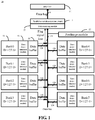
- FIG. 1 schematically illustrates a block diagram of a partial structure of a semiconductor memory according to an implementation of the embodiments.
- the semiconductor memory 20 includes a DQ port 24, a memory bank 26, and a read operation circuit.
- the read operation circuit includes a global bus, an inversion flag signal line, a data determination module 23, a data buffer 22, a data receiving module 25, and a parallel-to-serial conversion circuit 21.
- the semiconductor memory 20 is a dynamic random access memory (DRAM), such as a double data rate SDRAM 4 (DDR4).
- DRAM dynamic random access memory
- an active command can enable the only designated memory bank 26, and the read operation can only be performed on one memory bank 26. That is, when one memory bank among eight memory banks 26 (i.e. Bank ⁇ 7:0>) is operating, the other memory banks are not operating.
- the read data D ⁇ 127:0> in the memory bank 26 outputs 8-bit output data DQ ⁇ 7:0> through the DQ port 24.
- the number of memory banks 26, the number of data bits of each memory bank 26, and the number of data bits of the DQ port 24 and the number of DQ ports 24 are not limited in this embodiment. For example, there may be one DQ port 24 configured to output 16-bit output data, or there may be two DQ ports 24, and each of the two DQ ports 24 is configured to output 8-bit output data.
- the output data DQ ⁇ 7:0> is obtained by performing a read operation on a group of memory banks Bank ⁇ 7:0> by one of the read operation circuits mentioned above
- the output data DQ ⁇ 15:8> is obtained by performing a read operation on another group of memory banks Bank ⁇ 15:8> by another one of the read operation circuits mentioned above.
- the other memory banks are not operating.
- the semiconductor memory 20 has an array structure, and the units may have the same structure. However, because inputted data are different, data output by the various units may be different from each other.
- the read operation circuit of this embodiment is introduced below by taking one of the memory banks as an example.
- the data determination module 23 is connected to the memory bank 26 and is configured to read read data such as D ⁇ 127:0> from the memory bank 26, and determine whether to invert the read data according to the number of bits of high data in the read data to output global bus data for transmission through a global bus and inversion flag data for transmission through an inversion flag signal line.
- High data may be data equal to "1”
- low data may be data equal to "0”.
- Inversion of data may be understood as inversion from “0” to "1”, or inversion from " 1" to "0”.
- the inversion of a data line or a signal line may be understood as inversion from a high level to a low level, or inversion from a low level to a high level.
- the data determination module 23 is configured to: output inverted data of the read data as the global bus data and set the inversion flag data to High, if the number of bits of the high data in the read data is greater than a preset value; and output original read data as the global bus data and set the inversion flag data to Low, if the number of bits of the high data in the read data is less than or equal to the preset value.
- multi-bit read data is not grouped. That is, the inversion flag data may be 1-bit data. In an example, multi-bit read data may be grouped. For example, in an embodiment, each of the read data and the global bus data is divided into M groups, the inversion flag data has M bits, the M-bit inversion flag data corresponds to the M groups of read data one to one, and the M-bit inversion flag data corresponds to the M groups of global bus data one to one, where the M is an integer greater than 1.
- each group of read data has N bits, where the N is an integer greater than 1.
- the data determination module 23 is configured to: output inverted data of a group of input read data as a corresponding group of global bus data and set 1-bit inversion flag data corresponding to the group of input read data to High, if the number of bits of the high data in the group of input read data is greater than N/2; and output a group of input read data as a corresponding group of global bus data and set 1-bit inversion flag data corresponding to the group of input read data to Low, if the number of bits of the high data in the group of input read data is less than or equal to N/2.
- the read data D ⁇ 127:0> is divided into 16 groups, each group of read data has 8 bits, and each group of read data corresponds to 1-bit inversion flag data.
- the inversion flag data has 16 bits, such as Flag ⁇ 15:0>.
- the global bus data Dl' ⁇ 127:0> will also be divided into 16 groups accordingly.
- Each 1-bit inversion flag data corresponds to a group of global bus data.
- the global bus data Dl' ⁇ 127:120> output from the data determination module 23 is the inverted data of the read data D ⁇ 127:120> of the memory bank 26 (such as BankO).
- the global bus data Dl' ⁇ 15:8> output from the data determination module 23 is the inverted data of the read data D ⁇ 15:8> of the memory bank 26 (such as BankO).
- the global bus data Dl' ⁇ 7:0> output from the data determination module 23 is the inverted data of the read data D ⁇ 7:0> of the memory bank 26 (such as BankO).
- each of the plurality of global buses transmits 1-bit global bus data.
- M is an integer greater than 1
- each of the plurality of global buses transmits 1-bit global bus data.
- the global bus ⁇ 0> transmits global bus data D1' ⁇ 0>; the global bus ⁇ 1> transmits global bus data D1' ⁇ 1>; ...; and the global bus ⁇ 127> transmits global bus data D1' ⁇ 127>.
- each inversion flag signal line transmits 1-bit inversion flag data.
- the inversion flag signal line ⁇ 0> transmits inversion flag data Flag ⁇ 0>, and corresponds to the global bus data Dl' ⁇ 7:0> to represent whether Dl' ⁇ 7:0> is inverted data.
- the inversion flag signal line ⁇ 1> transmits inversion flag data Flag ⁇ 1>, and corresponds to the global bus data Dl' ⁇ 15:8> to represent whether Dl' ⁇ 15 :8> is inverted data; ...; and the inversion flag signal line ⁇ 15> transmits inversion flag data Flag ⁇ 15>, and corresponds to the global bus data Dl' ⁇ 127:120> to represent whether D1' ⁇ 127:120> is inverted data.
- the data buffer 22 is connected to the memory bank 26 through the global bus, and the precharge module 27 is connected to a precharge signal line and is configured to set an initial state of the global bus to Low. That is, in this embodiment, the semiconductor memory 20 uses a precharge low global bus transmission structure.
- FIG. 3 schematically illustrates a circuit diagram (corresponding to one memory bank 26) of the data buffer 22 and the precharge module 27 according to an implementation of the embodiments.
- FIG. 4 schematically illustrates a circuit diagram (corresponding to eight memory banks 26) of the data buffer 22 and the precharge module 27 according to an implementation of the embodiments.
- the data buffer 22 includes a plurality of Positive Channel Metal Oxide Semiconductor (PMOS) transistors 221, and the precharge module 27 includes a plurality of Negative Channel Metal Oxide Semiconductor (NMOS) transistors 222 and a plurality of hold circuits 223.
- a gate of each of the plurality of PMOS transistors 221 is connected to the memory bank 26, and a drain of each of the plurality of PMOS transistors 221 is connected to the global bus.
- Agate of each of the plurality of NMOS transistors 222 is connected to the precharge signal line, and a drain of each of the plurality of NMOS transistors 222 is connected to the global bus.
- An input terminal and an output terminal of each of the plurality of hold circuits 223 are connected to the global bus to form a positive feedback circuit.
- the precharge signal line is configured to set the initial state of each global bus to Low.
- a pull-down pulse (a pulse for approximately 2ns) is generated by the precharge signal line to pull down a certain global bus for a moment, and the hold circuit 223 forms a positive feedback and latches this global bus at a low level.
- the hold circuit 223 has weaker capability in pulling up and pulling down electric current.
- a data line i.e., a data line connected to the gate of the corresponding one of the plurality of PMOS transistors 221) corresponding to this global bus is pulled down (which is also a pulse for approximately 2ns), such that the PMOS transistor 221 pulls up this global bus for a moment (the pull-up capability is better than the pull-down capability of the hold circuit 223).
- this global bus is latched to a high level through the positive feedback. In this way, inversion of the data line is completed.
- IDD4R read current
- the data determination module 230 includes a data determination unit 231 and a data selector 232.
- An input terminal of the data determination unit 231 is connected to the memory bank 26 through a local bus, and an output terminal of the data determination unit 231 is connected to the inversion flag signal line and is connected to an input terminal of the data selector 232.
- the data determination unit 231 is configured to set the inversion flag data to High if the number of bits of the high data in the read data is greater than a preset value, and set the inversion flag data to Low if the number of bits of the high data in the read data is less than or equal to the preset value.
- the data determination unit 231 may include a plurality of data determination subunits, and each of the plurality of data determination subunits is configured to process a group of read data, and then output 1-bit inversion flag data.
- each of the plurality of data determination subunits is configured to process a group of read data, and then output 1-bit inversion flag data.
- An input terminal of the data selector 232 is connected to the data determination unit 231 to receive the read data through the data determination unit 231, the input terminal of the data selector 232 is configured to receive the inversion flag data through the inversion flag signal line, and an output terminal of the data selector 232 is connected to the global bus.
- the data selector 232 is configured to output inverted data of the read data as the global bus data if the inversion flag data is High, and output original read data as the global bus data if the inversion flag data is Low.
- the data selector 232 includes a plurality of data selection units 232', and each of the plurality of data selection units 232' is configured to process 1-bit inversion flag data and a group of read data.
- each of the plurality of data selection units 232' is configured to process 1-bit inversion flag data and a group of read data.
- FIG. 6 illustrates an implementation of the data selection unit 232'.
- the data selection unit 232' includes a first inverter 232A, a second inverter 232B, a first transmission gate 232C, and a second transmission gate 232D.
- An input terminal of the first inverter 232A is configured to receive the inversion flag data through the inversion flag signal line.
- An input terminal of the second inverter 232B is connected to the data determination unit 231 to receive the read data from the data determination unit 231.
- An input terminal of the first transmission gate 232C is connected to an output terminal of the second inverter 232B, an output terminal of the first transmission gate 232C is connected to the global bus to output the global bus data, a negative control terminal (the upper control terminal in FIG 6 ) of the first transmission gate 232C is connected to an output terminal of the first inverter 232A, and a positive control terminal (the lower control terminal in FIG.
- the first transmission gate 232C is configured to receive the inversion flag data through the inversion flag signal line.
- An input terminal of the second transmission gate 232D is connected to the data determination unit 231 to receive the read data from the data determination unit 231, an output terminal of the second transmission gate 232D is connected to the global bus to output the global bus data, a negative control terminal of the second transmission gate 232D is configured to the inversion flag data through the inversion flag signal line, and a positive control terminal of the second transmission gate 232D is connected to the output terminal of the first inverter 232A.
- a group of second inverter 232B, first transmission gate 232C and second transmission gate 232D is configured to process 1-bit read data and output 1-bit corresponding global bus data. That is, corresponding to 8-bit read data D ⁇ 7:0>, there will be eight groups of second inverters 232B, first transmission gates 232C and second transmission gates 232D, and then 8-bit global bus data Dl' ⁇ 7:0> is output.
- the read operation circuit in this embodiment further includes a data receiving module 25 connected to the global bus and the inversion flag signal line respectively and configured to determine whether to invert the global bus data according to the inversion flag data to output cache data.
- the data receiving module 25 is configured to output inverted data of the global bus data as the cache data if the inversion flag data is High, and output original global bus data as the cache data if the inversion flag data is Low.
- the cache data is recovered to the read data in the memory bank 26. Further, neither data nor functions of an external port such as the DQ port 24 and a DBI port (not illustrated in the figures) of the semiconductor memory 20 will be changed.
- the data receiving module 25 may include a plurality of data receiving units 250, and each of the plurality of data receiving units 250 is configured to process 1-bit inversion flag data and a group of global bus data.
- each of the plurality of data receiving units 250 is configured to process 1-bit inversion flag data and a group of global bus data.
- FIG. 8 illustrates an implementation of the data receiving units 250.
- the data receiving unit 250 includes a third inverter 251, a fourth inverter 252, a third transmission gate 253, and a fourth transmission gate 254.
- An input terminal of the third inverter 251 is configured to receive the flag data through the inversion flag signal line.
- An input terminal of the fourth inverter 252 is configured to receive the global bus data through the global bus.
- An input terminal of the third transmission gate 253 is connected to an output terminal of the fourth inverter 252, an output terminal of the third transmission gate 253 is connected to the parallel-to-serial conversion circuit 21 to output the cache data to the parallel-to-serial conversion circuit 21, a negative control terminal (the upper control terminal in FIG. 8 ) of the third transmission gate 253 is connected to an output terminal of the third inverter 251, and a positive control terminal of the third transmission gate 253 is configured to receive the inversion flag data through the inversion flag signal line.
- An input terminal of the fourth transmission gate 254 is configured to receive the global bus data through the global bus, an output terminal of the fourth transmission gate 254 is connected to the parallel-to-serial conversion circuit 21 to output the cache data to the parallel-to-serial conversion circuit 21, a negative control terminal (the upper control terminal in FIG. 8 ) of the fourth transmission gate 254 is configured to receive the inversion flag data through the inversion flag signal line, and a positive control terminal (the lower control terminal in FIG. 8 ) of the fourth transmission gate 254 is connected to the output terminal of the third inverter 251.
- a group of fourth inverter 252, third transmission gate 253 and fourth transmission gate 254 is configured to process 1-bit global bus data and output corresponding 1-bit cache data. That is, corresponding to 8-bit global bus data Dl' ⁇ 7:0>, there wil be eight groups of fourth inverters 252, third transmission gates 253 and fourth transmission gates 254, and then 8-bit cache data D2' ⁇ 7:0> is output.
- the read operation circuit in this embodiment further includes a parallel-to-serial conversion circuit 21.
- the parallel-to-serial conversion circuit 21 is connected to the data receiving module 25 to perform parallel-to-serial conversion on the cache data to generate output data of the DQ port 24.
- the parallel-to-serial conversion circuit 21 performs parallel-to-serial conversion on 128-bit cache data D2' ⁇ 127:0> corresponding to Bank 0 to generate 8-bit output data DQ ⁇ 7:0>.
- the global bus data has 256 bits. If it is needed to invert 256-bit global bus data, it is only needed to invert 32-bit inversion flag data, such that the IDD4R electric current will be reduced significantly.
- the semiconductor memory 20 of this embodiment also includes other structures such as a sensitive amplifier and a precharge circuit, which will not be repeated in this embodiment because they belong to the existing technologies.
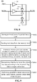
- FIG. 9 schematically illustrates a flowchart of a read operation method according to an implementation of the embodiments.
- the read operation method may be used in the semiconductor memory 20. As illustrated in FIG. 9 , the read operation method may include Steps S901 to S905.
- Step S901 an initial state of a global bus is set to Low.
- Step S902 read data is read from the memory bank.
- Step S903 whether to invert the read data is determined according to the number of bits of high data in the read data to output global bus data for transmission through the global bus and inversion flag data for transmission through an inversion flag signal line.
- Step S904 whether to invert the global bus data is determined according to the inversion flag data to output cache data; and In Step S905, parallel-to-serial conversion is performed on the cache data to generate output data of the DQ port.
- the Step S903 may include: outputting inverted data of the read data as the global bus data and setting the inversion flag data to High, if the number of bits of the high data in the read data is greater than a preset value; and outputting original read data as the global bus data and setting the inversion flag data to Low, if the number of bits of the high data in the read data is less than or equal to the preset value.
- the Step S903 may include: dividing the read data into M groups, wherein each group of read data has N bits, and both the M and the N are integers greater than 1; outputting inverted data of a group of input read data as a corresponding group of global bus data and setting 1-bit inversion flag data corresponding to the group of input read data to High, if the number of bits of high data in the group of input read data is greater than N/2; and outputting a group of input read data as a corresponding group of global bus data and setting 1-bit inversion flag data corresponding to the group of input read data to Low, if the number of bits of the high data in the group of input read data is less than or equal to N/2.
- the read operation circuit provided by the embodiments of the present disclosure is used in a semiconductor memory of which global bus transmission structure is a precharge low architecture.
- global bus transmission structure is a precharge low architecture.
- first and second are used only for purposes of description and are not intended to indicate or imply relative importance or to imply the number of indicated technical features. Thus, the feature defined with “first” and “second” may explicitly or implicitly include at least one such feature. In the description of the present disclosure, “a plurality of' refers to at least two, unless otherwise expressly specified.
- steps of the method in the present disclosure are described in a particular order in the accompanying drawings. However, this does not require or imply to execute these steps necessarily according to the particular order, or this does not mean that the expected result cannot be implemented unless all the illustrated steps are executed. Additionally or alternatively, some steps may be omitted, a plurality of steps may be combined into one step for execution, and/or one step may be decomposed into a plurality of steps for execution.
- the above accompanying drawings are merely illustrative description of processes included in the method according to the exemplary embodiments of the present disclosure and are not intended to limit the present disclosure. It is easy to understand that the processes illustrated in the above accompanying drawings do not indicate or limit time sequences of these processes. Furthermore, it is also easy to understand that these processes may be executed, for example, synchronously or asynchronously in a plurality of modules.
Landscapes
- Engineering & Computer Science (AREA)
- Theoretical Computer Science (AREA)
- Microelectronics & Electronic Packaging (AREA)
- Computer Hardware Design (AREA)
- Human Computer Interaction (AREA)
- Physics & Mathematics (AREA)
- General Engineering & Computer Science (AREA)
- General Physics & Mathematics (AREA)
- Databases & Information Systems (AREA)
- Dram (AREA)
- Static Random-Access Memory (AREA)
Abstract
Description
- This application claims priority to
Chinese Patent Application No. 201911021459.9 - The present disclosure relates to the field of semiconductor memory technologies, and more particularly, to a read operation circuit, a semiconductor memory, and a read operation method.
- This section is intended to provide a background or context for embodiments the present disclosure that is recited in the claims. The description of this section is not to be admitted as prior art for the mere fact of being included in this section.
- A semiconductor memory includes a static random-access memory (SRAM), a dynamic random access memory (DRAM), a synchronous dynamic random access memory (SDRAM), a read-only memory (ROM), and a flash memory, etc.
- In a DRAM protocol of the Joint Electron Device Engineering Council (JEDEC), there are requirements for speed and power saving of the DRAM. How to ensure the DRAM to be more power-saving while ensuring the integrity of a signal and the reliability of data transmission and storage is a problem to be solved urgently in the industry.
- Embodiments of the present disclosure provide a read operation circuit, a semiconductor memory, and a read operation method to solve or alleviate one or more technical problems in the existing technologies.
- In a first aspect, the embodiments of the present disclosure provide a read operation circuit used in a semiconductor memory, wherein the semiconductor memory comprises a Data Queue (DQ) port and a memory bank. The read operation circuit comprising:
- a data determination module connecte d to the memory bank and configured to read read data from the memory bank, and determine whether to invert the read data according to the number of bits of high data in the read data to output global bus data for transmission through a global bus and inversion flag data for transmission through an inversion flag signal line;
- a data receiving module connected to the global bus and the inversion flag signal line and configured to determine whether to invert the global bus data according to the inversion flag data to output cache data;
- a parallel-to-serial conversion circuit connected between the data receiving module and the DQ port and configured to perform parallel-to-serial conversion on the cache data to generate output data of the DQ port;
- a data buffer connected to the memory bank through the global bus; and
- a precharge module connected to a precharge signal line and configured to set an initial state of the global bus to Low.
- In an implementation, the data determination module is configured to output inverted data of the read data as the global bus data and set the inversion flag data to High if the number of bits of the high data in the read data is greater than a preset value, and output original read data as the global bus data and set the inversion flag data to Low if the number of bits of the high data in the read data is less than or equal to the preset value.
- In an implementation, the read data and the global bus data are both divided into M groups, the inversion flag data having M bits, and the M-bit inversion flag data being corresponding to the M groups of read data one to one, and the M-bit inversion flag data being corresponding to the M groups of global bus data one to one, where the M is an integer greater than 1.
- In an implementation, each group of read data has N bits, wherein the N being an integer greater than 1. The data determination module being configured to output inverted data of a group of input read data as a corresponding group of global bus data and set 1-bit inversion flag data corresponding to the group of input read data to High if the number of bits of the high data in the group of input read data is greater than N/2, and output a group of input read data as a corresponding group of global bus data and set 1-bit inversion flag data corresponding to the group of input read data to Low if the number of bits of high data in the group of input read data is less than or equal to N/2.
- In an implementation, the data determination module comprises:
- a data determination unit, an input terminal of the data determination unit being connected to the memory bank, an output terminal of the data determination unit being connected to the inversion flag signal line, and the data determination unit being configured to set the inversion flag data to High if the number of bits of the high data in the read data is greater than a preset value, and set the inversion flag data to Low if the number of bits of the high data in the read data is less than or equal to the preset value; and
- a data selector, an input terminal of the data selector being connected to the data determination unit to receive the read data through the data determination unit, and the input terminal of the data selector being configured to receive the inversion flag data through the inversion flag signal line, an output terminal of the data selector being connected to the global bus, and the data selector is configured to output inverted data of the read data as the global bus data if the inversion flag data is High, and output original read data as the global bus data if the inversion flag data is Low.
- In an implementation, the data selector comprises a plurality of data selection units, each of the plurality of data selection units comprising:
- a first inverter, an input terminal of the first inverter being configured to receive the inversion flag data through the inversion flag signal line;
- a second inverter, an input terminal of the second inverter being connected to the data determination unit to receive the read data from the data determination unit;
- a first transmission gate, an input terminal of the first transmission gate being connected to an output terminal of the second inverter, an output terminal of the first transmission gate being connected to the global bus to output the global bus data, a negative control terminal of the first transmission gate being connected to an output terminal of the first inverter, and a positive control terminal of the first transmission gate being configured to receive the inversion flag data through the inversion flag signal line; and
- a second transmission gate, an input terminal of the second transmission gate being connected to the data determination unit to receive the read data from the data determination unit, an output terminal of the second transmission gate being connected to the global bus to output the global bus data, a negative control terminal of the second transmission gate being configured to receive the inversion flag data through the inversion flag signal line, and a positive control terminal of the second transmission gate being connected to the output terminal of the first inverter.
- In an implementation, the data receiving module is configured to output inverted data of the global bus data as the cache data if the inversion flag data is High, and output original global bus data as the cache data if the inversion flag data is Low.
- In an implementation, the data receiving module comprises a plurality of data receiving units, each of the plurality of data receiving units comprising:
- a third inverter, an input terminal of the third inverter being configured to receive the inversion flag data through the inversion flag signal line;
- a fourth inverter, an input terminal of the fourth inverter being configured to receive the global bus data through the global bus;
- a third transmission gate, an input terminal of the third transmission gate being connected to an output terminal of the fourth inverter, an output terminal of the third transmission gate being connected to the parallel-to-serial conversion circuit to output the cache data to the parallel-to-serial conversion circuit, a negative control terminal of the third transmission gate being connected to an output terminal of the third inverter, and a positive control terminal of the third transmission gate being configured to receive the inversion flag data through the inversion flag signal line; and
- a fourth transmission gate, an input terminal of the fourth transmission gate being configured to receive the global bus data through the global bus, an output terminal of the fourth transmission gate being connected to the parallel-to-serial conversion circuit to output the cache data to the parallel-to-serial conversion circuit, a negative control terminal of the fourth transmission gate being configured to receive the inversion flag data through the inversion flag signal line, and a positive control terminal of the fourth transmission gate being connected to the output terminal of the third inverter.
- In an implementation, the data buffer comprises a plurality of PMOS transistors, wherein a gate of each of the plurality of PMOS transistors being connected to the memory bank, and a drain of each of the plurality of PMOS transistors being connected to the global bus. The precharge module comprises a plurality of NMOS transistors and a plurality of hold circuits, a gate of each of the plurality of NMOS transistors being connected to the precharge signal line, and a drain of each of the plurality of NMOS transistors being connected to the global bus. An input terminal and an output terminal of each of the plurality of hold circuits being connected to the global bus.
- In a second aspect, the embodiments of the present disclosure provide a semiconductor memory, which includes a DQ port, a memory bank, and the read operation circuit according to any one of the above implementations.
- In a third aspect, the embodiments of the present disclosure provide a read operation method used in a semiconductor memory, wherein the semiconductor memory includes a DQ port and a memory bank. The read operation method comprising:
- setting an initial state of a global bus to Low;
- reading read data from the memory bank;
- determining whether to invert the read data according to the number of bits of high data in the read data to output global bus data for transmission through the global bus and inversion flag data for transmission through an inversion flag signal line;
- determining whether to invert the global bus data according to the inversion flag data to output cache data; and
- performing parallel-to-serial conversion on the cache data to generate output data of the DQ port.
- In an implementation, the determining whether to invert the read data according to the number of bits of high data in the read data to output global bus data for transmission through the global bus and inversion flag data for transmission through an inversion flag signal line comprises:
- outputting inverted data of the read data as the global bus data and setting the inversion flag data to High if the number of bits of the high data in the read data is greater than a preset value; and
- outputting original read data as the global bus data and setting the inversion flag data to Low if the number of bits of the high data in the read data is less than or equal to the preset value.
- In an implementation, the determining whether to invert the read data according to the number of bits of high data in the read data to output global bus data for transmission through the global bus and inversion flag data for transmission through an inversion flag signal line comprises:
- dividing the read data into M groups, wherein each group of read data has N bits, and both the M and the N are integers greater than 1;
- outputting inverted data of a group of input read data as a corresponding group of global bus data and setting 1-bit inversion flag data corresponding to the group of input read data to High if the number of bits of high data in the group of input read data is greater than N/2; and
- outputting a group of input read data as a corresponding group of global bus data and setting 1-bit inversion flag data corresponding to the group of input read data to Low if the number of bits of high data in the group of input read data is less than or equal to N/2.
- According to the technical solutions of the embodiments of the present disclosure, more data "0" can be transmitted through a global bus having a precharge low architecture, such that the number of inversions of the internal global bus can be reduced. In this way, electric current is reduced significantly, and power consumption is decreased.
- The above summary is for the purpose of illustration only and is not intended to be limiting in any way. In addition to the illustrative aspects, embodiments, and features described above, further aspects, embodiments, and features of the present disclosure will be readily apparent by reference to the drawings and the following detailed description.
- In the drawings, the same reference numerals denote the same or similar parts or elements throughout the various drawings unless otherwise specified. These drawings are not necessarily drawn to scale. It is to be understood that these drawings depict only some embodiments disclosed according to the present disclosure and is not to be deemed as limitations on the scope of the present disclosure.
-
FIG. 1 schematically illustrates a block diagram of a partial structure of a semiconductor memory according to an implementation of the embodiments; -
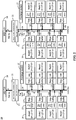
FIG. 2 schematically illustrates a block diagram of a partial structure of the semiconductor memory according to another implementation of the embodiments; -
FIG. 3 schematically illustrates a circuit diagram (corresponding to one memory bank) of a data buffer and a precharge module according to an implementation of the embodiments; -
FIG. 4 schematically illustrates a circuit diagram (corresponding to a plurality of memory banks) of the data buffer and the precharge module according to an implementation of the embodiments; -
FIG. 5 schematically illustrates a block diagram of a data determination module according to an implementation of the embodiments; -
FIG. 6 schematically illustrates a block diagram of a data selection unit according to an implementation of the embodiments; -
FIG. 7 schematically illustrates a block diagram of a data receiving module according to an implementation of the embodiments; -
FIG. 8 schematically illustrates a block diagram of a data receiving unit according to an implementation of the embodiments; and -
FIG. 9 schematically illustrates a flowchart of a read operation method according to an implementation of the embodiments. - Reference numbers in the accompanying drawings:
- 20: semiconductor memory;
- 21: parallel-to-serial conversion circuit;
- 22: data buffer;
- 23: data determination module;
- 24: DQ port;
- 25: data receiving module;
- 26: memory bank;
- 27: precharge module;
- 221: PMOS transistor;
- 222: NMOS transistor;
- 223: hold circuit;
- 231: data determination unit;
- 232: data selector;
- 232': data selection unit;
- 232A: first inverter;
- 232B: second inverter;
- 232C: first transmission gate;
- 232D: second transmission gate;
- 250: data receiving unit;
- 251: third inverter;
- 252: fourth inverter;
- 253: third transmission gate; and
- 254: fourth transmission gate.
- The exemplary embodiment will now be described more fully with reference to the accompanying drawings. However, the exemplary embodiments can be implemented in a variety of forms and is not to be construed as being limited to the embodiments set forth herein. Instead, these embodiments are provided such that the present disclosure will be thorough and complete and will fully convey the concepts of the exemplary embodiments to those skilled in the art. The same reference numerals in the drawings denote the same or similar parts, and thus repeated description thereof will be omitted.
-
FIG. 1 schematically illustrates a block diagram of a partial structure of a semiconductor memory according to an implementation of the embodiments. As illustrated inFIG. 1 , thesemiconductor memory 20 includes aDQ port 24, amemory bank 26, and a read operation circuit. The read operation circuit includes a global bus, an inversion flag signal line, adata determination module 23, adata buffer 22, adata receiving module 25, and a parallel-to-serial conversion circuit 21. In an embodiment, thesemiconductor memory 20 is a dynamic random access memory (DRAM), such as a double data rate SDRAM 4 (DDR4). - In an example, as illustrated in
FIG. 1 , an active command can enable the only designatedmemory bank 26, and the read operation can only be performed on onememory bank 26. That is, when one memory bank among eight memory banks 26 (i.e. Bank<7:0>) is operating, the other memory banks are not operating. By means of the read operation circuit, the read data D<127:0> in thememory bank 26 outputs 8-bit output data DQ<7:0> through theDQ port 24. It is to be noted that the number ofmemory banks 26, the number of data bits of eachmemory bank 26, and the number of data bits of theDQ port 24 and the number ofDQ ports 24 are not limited in this embodiment. For example, there may be oneDQ port 24 configured to output 16-bit output data, or there may be twoDQ ports 24, and each of the twoDQ ports 24 is configured to output 8-bit output data. - For example, as illustrated in
FIG. 2 , the output data DQ<7:0> is obtained by performing a read operation on a group of memory banks Bank<7:0> by one of the read operation circuits mentioned above, and the output data DQ<15:8> is obtained by performing a read operation on another group of memory banks Bank<15:8> by another one of the read operation circuits mentioned above. Correspondingly, when one of the eight memory banks 26 (i.e., Bank<15:8>) corresponding to the output data DQ<15:8> is operating, the other memory banks are not operating. - The
semiconductor memory 20 has an array structure, and the units may have the same structure. However, because inputted data are different, data output by the various units may be different from each other. The read operation circuit of this embodiment is introduced below by taking one of the memory banks as an example. - The
data determination module 23 is connected to thememory bank 26 and is configured to read read data such as D<127:0> from thememory bank 26, and determine whether to invert the read data according to the number of bits of high data in the read data to output global bus data for transmission through a global bus and inversion flag data for transmission through an inversion flag signal line. High data may be data equal to "1", and low data may be data equal to "0". Inversion of data may be understood as inversion from "0" to "1", or inversion from " 1" to "0". The inversion of a data line or a signal line may be understood as inversion from a high level to a low level, or inversion from a low level to a high level. - In an embodiment, the
data determination module 23 is configured to: output inverted data of the read data as the global bus data and set the inversion flag data to High, if the number of bits of the high data in the read data is greater than a preset value; and output original read data as the global bus data and set the inversion flag data to Low, if the number of bits of the high data in the read data is less than or equal to the preset value. - In an example, multi-bit read data is not grouped. That is, the inversion flag data may be 1-bit data. In an example, multi-bit read data may be grouped. For example, in an embodiment, each of the read data and the global bus data is divided into M groups, the inversion flag data has M bits, the M-bit inversion flag data corresponds to the M groups of read data one to one, and the M-bit inversion flag data corresponds to the M groups of global bus data one to one, where the M is an integer greater than 1.
- Further, each group of read data has N bits, where the N is an integer greater than 1. The
data determination module 23 is configured to: output inverted data of a group of input read data as a corresponding group of global bus data and set 1-bit inversion flag data corresponding to the group of input read data to High, if the number of bits of the high data in the group of input read data is greater than N/2; and output a group of input read data as a corresponding group of global bus data and set 1-bit inversion flag data corresponding to the group of input read data to Low, if the number of bits of the high data in the group of input read data is less than or equal to N/2. - For example, the read data D<127:0> is divided into 16 groups, each group of read data has 8 bits, and each group of read data corresponds to 1-bit inversion flag data. Correspondingly, the inversion flag data has 16 bits, such as Flag<15:0>. The global bus data Dl'<127:0> will also be divided into 16 groups accordingly. Each 1-bit inversion flag data corresponds to a group of global bus data. For a group of read data D<127:120>, if the number of bits equal to "1" in D<127:120> is greater than 4 bits, the corresponding Flag<15>=1, and a group of output global bus data D1 '<120:127> is equal to the inverted data of D<127:120>; and if the number of bits equal to "1" in the read data is less than or equal to 4 bits, the corresponding Flag<15>=0, and a group of global bus data D1'< 120:127> output is D<127:120>.
- Hence, when Flag<15>=1, the global bus data Dl'<127:120> output from the
data determination module 23 is the inverted data of the read data D<127:120> of the memory bank 26 (such as BankO). When Flag<15>=0, the global bus data Dl'<127:120> output from thedata determination module 23 is the read data D<127:120> of the memory bank 26 (such as BankO). That is, the read data D1'<127:120>=D<127:120>. Similarly, when Flag<1>=1, the global bus data Dl'<15:8> output from thedata determination module 23 is the inverted data of the read data D<15:8> of the memory bank 26 (such as BankO). When Flag<1>=0, the global bus data Dl'<15:8> output from thedata determination module 23 is the read data D<15:8> of the memory bank 26 (such as BankO). That is, the global bus data D1'<15:8>=D<15:8>. When Flag<0>=1, the global bus data Dl'<7:0> output from thedata determination module 23 is the inverted data of the read data D<7:0> of the memory bank 26 (such as BankO). When the Flag<0>=0, the global bus data Dl'<7:0> output from thedata determination module 23 is the read data D<7:0> of the memory bank 26 (such as BankO). That is, the global bus data Dl'<7:0>=D<7:0>. - In an example, there are a plurality of global buses, which are divided into M (M is an integer greater than 1) groups, wherein each of the plurality of global buses transmits 1-bit global bus data. For example, there are 128 global buses, which are divided into 16 groups. The global bus <0> transmits global bus data D1'<0>; the global bus <1> transmits global bus data D1'<1>; ...; and the global bus <127> transmits global bus data D1'<127>.
- In an example, there are 16 inversion flag signal lines, and each inversion flag signal line transmits 1-bit inversion flag data. For example, the inversion flag signal line <0> transmits inversion flag data Flag<0>, and corresponds to the global bus data Dl'<7:0> to represent whether Dl'<7:0> is inverted data. The inversion flag signal line <1> transmits inversion flag data Flag<1>, and corresponds to the global bus data Dl'<15:8> to represent whether Dl'<15 :8> is inverted data; ...; and the inversion flag signal line <15> transmits inversion flag data Flag<15>, and corresponds to the global bus data Dl'<127:120> to represent whether D1'<127:120> is inverted data.
- Thus, there are more data "0" among the global bus data D1'<127:0> transmitted through the global bus. Accordingly, in the
semiconductor memory 20 as illustrated inFIG. 2 , there are more data "0" among the 256-bit global bus data (including the 128-bit global bus data corresponding to DQ<7:0> and the 128-bit global bus data corresponding to DQ<15:8>). - The
data buffer 22 is connected to thememory bank 26 through the global bus, and theprecharge module 27 is connected to a precharge signal line and is configured to set an initial state of the global bus to Low. That is, in this embodiment, thesemiconductor memory 20 uses a precharge low global bus transmission structure. -
FIG. 3 schematically illustrates a circuit diagram (corresponding to one memory bank 26) of thedata buffer 22 and theprecharge module 27 according to an implementation of the embodiments.FIG. 4 schematically illustrates a circuit diagram (corresponding to eight memory banks 26) of thedata buffer 22 and theprecharge module 27 according to an implementation of the embodiments. - As illustrated in
FIG. 3 and FIG. 4 , thedata buffer 22 includes a plurality of Positive Channel Metal Oxide Semiconductor (PMOS)transistors 221, and theprecharge module 27 includes a plurality of Negative Channel Metal Oxide Semiconductor (NMOS)transistors 222 and a plurality ofhold circuits 223. A gate of each of the plurality ofPMOS transistors 221 is connected to thememory bank 26, and a drain of each of the plurality ofPMOS transistors 221 is connected to the global bus. Agate of each of the plurality ofNMOS transistors 222 is connected to the precharge signal line, and a drain of each of the plurality ofNMOS transistors 222 is connected to the global bus. An input terminal and an output terminal of each of the plurality ofhold circuits 223 are connected to the global bus to form a positive feedback circuit. - The precharge signal line is configured to set the initial state of each global bus to Low. In this process, a pull-down pulse (a pulse for approximately 2ns) is generated by the precharge signal line to pull down a certain global bus for a moment, and the
hold circuit 223 forms a positive feedback and latches this global bus at a low level. However, thehold circuit 223 has weaker capability in pulling up and pulling down electric current. When a certain global bus needs to be inverted to a high level, a data line (i.e., a data line connected to the gate of the corresponding one of the plurality of PMOS transistors 221) corresponding to this global bus is pulled down (which is also a pulse for approximately 2ns), such that thePMOS transistor 221 pulls up this global bus for a moment (the pull-up capability is better than the pull-down capability of the hold circuit 223). Next, this global bus is latched to a high level through the positive feedback. In this way, inversion of the data line is completed. There are more data "0" among the global bus data Dl'<127:0>, and thus fewer inversions are required. Therefore, the IDD4R (read current) of the semiconductor memory will be reduced, such that the power consumption of the semiconductor memory can be reduced. - In an embodiment, as illustrated in
FIG. 5 , the data determination module 230 includes adata determination unit 231 and adata selector 232. - An input terminal of the
data determination unit 231 is connected to thememory bank 26 through a local bus, and an output terminal of thedata determination unit 231 is connected to the inversion flag signal line and is connected to an input terminal of thedata selector 232. Thedata determination unit 231 is configured to set the inversion flag data to High if the number of bits of the high data in the read data is greater than a preset value, and set the inversion flag data to Low if the number of bits of the high data in the read data is less than or equal to the preset value. - In an example, the
data determination unit 231 may include a plurality of data determination subunits, and each of the plurality of data determination subunits is configured to process a group of read data, and then output 1-bit inversion flag data. For example, there may be 16 data selection unit subunits, which are respectively corresponding to 16 groups of read data, and then 16-bit inversion flag data is output, wherein each group of read data may have 8 bits. - An input terminal of the
data selector 232 is connected to thedata determination unit 231 to receive the read data through thedata determination unit 231, the input terminal of thedata selector 232 is configured to receive the inversion flag data through the inversion flag signal line, and an output terminal of thedata selector 232 is connected to the global bus. Thedata selector 232 is configured to output inverted data of the read data as the global bus data if the inversion flag data is High, and output original read data as the global bus data if the inversion flag data is Low. - In an embodiment, the
data selector 232 includes a plurality of data selection units 232', and each of the plurality of data selection units 232' is configured to process 1-bit inversion flag data and a group of read data. For example, there may be 16 data selection units 232', which are respectively corresponding to 16 groups of read data and 1-bit inversion flag data, wherein each group of read data may have 8 bits. -
FIG. 6 illustrates an implementation of the data selection unit 232'. As illustrated inFIG. 6 , the data selection unit 232' includes afirst inverter 232A, asecond inverter 232B, afirst transmission gate 232C, and asecond transmission gate 232D. - An input terminal of the
first inverter 232A is configured to receive the inversion flag data through the inversion flag signal line. An input terminal of thesecond inverter 232B is connected to thedata determination unit 231 to receive the read data from thedata determination unit 231. An input terminal of thefirst transmission gate 232C is connected to an output terminal of thesecond inverter 232B, an output terminal of thefirst transmission gate 232C is connected to the global bus to output the global bus data, a negative control terminal (the upper control terminal inFIG 6 ) of thefirst transmission gate 232C is connected to an output terminal of thefirst inverter 232A, and a positive control terminal (the lower control terminal inFIG. 6 ) of thefirst transmission gate 232C is configured to receive the inversion flag data through the inversion flag signal line. An input terminal of thesecond transmission gate 232D is connected to thedata determination unit 231 to receive the read data from thedata determination unit 231, an output terminal of thesecond transmission gate 232D is connected to the global bus to output the global bus data, a negative control terminal of thesecond transmission gate 232D is configured to the inversion flag data through the inversion flag signal line, and a positive control terminal of thesecond transmission gate 232D is connected to the output terminal of thefirst inverter 232A. - Taking Flag<0> and the read data D<7:0> as an example, as illustrated in
FIG. 6 , when Flag=1, the global bus data Dl'<7:0> is the inverted data of the read data D<7:0>; and when Flag=0, the global bus data Dl'<7:0> is the read data D<7:0>. - It is to be noted that a group of
second inverter 232B,first transmission gate 232C andsecond transmission gate 232D is configured to process 1-bit read data and output 1-bit corresponding global bus data. That is, corresponding to 8-bit read data D<7:0>, there will be eight groups ofsecond inverters 232B,first transmission gates 232C andsecond transmission gates 232D, and then 8-bit global bus data Dl'<7:0> is output. - As illustrated in
FIG. 1 ,FIG. 2 andFIG. 7 , the read operation circuit in this embodiment further includes adata receiving module 25 connected to the global bus and the inversion flag signal line respectively and configured to determine whether to invert the global bus data according to the inversion flag data to output cache data. For example, thedata receiving module 25 is configured to output inverted data of the global bus data as the cache data if the inversion flag data is High, and output original global bus data as the cache data if the inversion flag data is Low. - Thus, the cache data is recovered to the read data in the
memory bank 26. Further, neither data nor functions of an external port such as theDQ port 24 and a DBI port (not illustrated in the figures) of thesemiconductor memory 20 will be changed. - In an embodiment, the
data receiving module 25 may include a plurality ofdata receiving units 250, and each of the plurality ofdata receiving units 250 is configured to process 1-bit inversion flag data and a group of global bus data. For example, there may be 16data receiving units 250, which are respectively corresponding to 16 groups of global bus data and 1-bit inversion flag data.FIG. 8 illustrates an implementation of thedata receiving units 250. - As illustrated in
FIG. 8 , thedata receiving unit 250 includes athird inverter 251, afourth inverter 252, athird transmission gate 253, and afourth transmission gate 254. - An input terminal of the
third inverter 251 is configured to receive the flag data through the inversion flag signal line. An input terminal of thefourth inverter 252 is configured to receive the global bus data through the global bus. An input terminal of thethird transmission gate 253 is connected to an output terminal of thefourth inverter 252, an output terminal of thethird transmission gate 253 is connected to the parallel-to-serial conversion circuit 21 to output the cache data to the parallel-to-serial conversion circuit 21, a negative control terminal (the upper control terminal inFIG. 8 ) of thethird transmission gate 253 is connected to an output terminal of thethird inverter 251, and a positive control terminal of thethird transmission gate 253 is configured to receive the inversion flag data through the inversion flag signal line. An input terminal of thefourth transmission gate 254 is configured to receive the global bus data through the global bus, an output terminal of thefourth transmission gate 254 is connected to the parallel-to-serial conversion circuit 21 to output the cache data to the parallel-to-serial conversion circuit 21, a negative control terminal (the upper control terminal inFIG. 8 ) of thefourth transmission gate 254 is configured to receive the inversion flag data through the inversion flag signal line, and a positive control terminal (the lower control terminal inFIG. 8 ) of thefourth transmission gate 254 is connected to the output terminal of thethird inverter 251. - Taking Flag<0> and the global bus data Dl'<7:0> as an example, as illustrated in
FIG. 8 , when Flag=1, the cache data D2'<7:0> is the inverted data of the global bus data Dl'<7:0>; and when Flag=0, the cache data D2'<7:0> is the global bus data Dl'<7:0>. That is, D2'<7:0>= D1'<7:0>. - It is to be noted that a group of
fourth inverter 252,third transmission gate 253 andfourth transmission gate 254 is configured to process 1-bit global bus data and output corresponding 1-bit cache data. That is, corresponding to 8-bit global bus data Dl'<7:0>, there wil be eight groups offourth inverters 252,third transmission gates 253 andfourth transmission gates 254, and then 8-bit cache data D2'<7:0> is output. - As illustrated in
FIG. 1 andFIG. 2 , the read operation circuit in this embodiment further includes a parallel-to-serial conversion circuit 21. The parallel-to-serial conversion circuit 21 is connected to thedata receiving module 25 to perform parallel-to-serial conversion on the cache data to generate output data of theDQ port 24. For example, the parallel-to-serial conversion circuit 21 performs parallel-to-serial conversion on 128-bit cache data D2'<127:0> corresponding toBank 0 to generate 8-bit output data DQ<7:0>. - According to the
semiconductor memory 20 of this embodiment, in the process of reading data (DQ<7:0>=<11111111>; DQ<15:8>=<11111111>) from thesemiconductor memory 20, the global bus data has 256 bits. If it is needed to invert 256-bit global bus data, it is only needed to invert 32-bit inversion flag data, such that the IDD4R electric current will be reduced significantly. - In practical applications, the
semiconductor memory 20 of this embodiment also includes other structures such as a sensitive amplifier and a precharge circuit, which will not be repeated in this embodiment because they belong to the existing technologies. -
FIG. 9 schematically illustrates a flowchart of a read operation method according to an implementation of the embodiments. The read operation method may be used in thesemiconductor memory 20. As illustrated inFIG. 9 , the read operation method may include Steps S901 to S905. - In Step S901, an initial state of a global bus is set to Low.
- In Step S902, read data is read from the memory bank.
- In Step S903, whether to invert the read data is determined according to the number of bits of high data in the read data to output global bus data for transmission through the global bus and inversion flag data for transmission through an inversion flag signal line.
- In Step S904, whether to invert the global bus data is determined according to the inversion flag data to output cache data; and
In Step S905, parallel-to-serial conversion is performed on the cache data to generate output data of the DQ port. - In an embodiment, the Step S903 may include: outputting inverted data of the read data as the global bus data and setting the inversion flag data to High, if the number of bits of the high data in the read data is greater than a preset value; and outputting original read data as the global bus data and setting the inversion flag data to Low, if the number of bits of the high data in the read data is less than or equal to the preset value.
- In an embodiment, the Step S903 may include: dividing the read data into M groups, wherein each group of read data has N bits, and both the M and the N are integers greater than 1; outputting inverted data of a group of input read data as a corresponding group of global bus data and setting 1-bit inversion flag data corresponding to the group of input read data to High, if the number of bits of high data in the group of input read data is greater than N/2; and outputting a group of input read data as a corresponding group of global bus data and setting 1-bit inversion flag data corresponding to the group of input read data to Low, if the number of bits of the high data in the group of input read data is less than or equal to N/2.
- The read operation circuit provided by the embodiments of the present disclosure is used in a semiconductor memory of which global bus transmission structure is a precharge low architecture. By inverting the read data by the data determination module, more data "0" can be transmitted through the global bus, such that the number of inversions of the internal global bus can be reduced. In this way, electric current can be reduced significantly, and power consumption can be decreased.
- Reference throughout this specification to the terms "an embodiment," "some embodiments," "one example," "an example," or "some examples," means that a feature, structure, material, or characteristic described in connection with the embodiment or example is included in at least one embodiment or example of the present disclosure. Furthermore, the features, structures, materials, or characteristics described may be combined in any suitable manner in one or more embodiments or examples. In addition, without contradiction, those skilled in the art may combine different embodiments or examples described in the specification and features of different embodiments or examples.
- In addition, the features, structures, or characteristics described may be combined in one or more embodiments in any suitable manner. However, those skilled in the art will appreciate that one or more of the details may be practiced without practicing the technical solutions of the present disclosure, and other methods, components, materials, devices, steps, and the like may be employed. In other instances, well-known structures, methods, devices, implementations, materials, or operations are not illustrated or described in detail to avoid obscuring aspects of the present disclosure.
- Terms "first" and "second" are used only for purposes of description and are not intended to indicate or imply relative importance or to imply the number of indicated technical features. Thus, the feature defined with "first" and "second" may explicitly or implicitly include at least one such feature. In the description of the present disclosure, "a plurality of' refers to at least two, unless otherwise expressly specified.
- It is to be noted that, steps of the method in the present disclosure are described in a particular order in the accompanying drawings. However, this does not require or imply to execute these steps necessarily according to the particular order, or this does not mean that the expected result cannot be implemented unless all the illustrated steps are executed. Additionally or alternatively, some steps may be omitted, a plurality of steps may be combined into one step for execution, and/or one step may be decomposed into a plurality of steps for execution. Moreover, the above accompanying drawings are merely illustrative description of processes included in the method according to the exemplary embodiments of the present disclosure and are not intended to limit the present disclosure. It is easy to understand that the processes illustrated in the above accompanying drawings do not indicate or limit time sequences of these processes. Furthermore, it is also easy to understand that these processes may be executed, for example, synchronously or asynchronously in a plurality of modules.
- In addition, although the spirit and the principle of the present disclosure have been described with reference to several embodiments, it is to be understood that the present disclosure is not limited to these embodiments disclosed, and the division of various aspects does not mean that the features in these aspects cannot be combined to get benefits, and this division is only for ease of expression. The present disclosure is intended to cover various modifications and equivalent arrangements included within the spirit and scope of the appended claims.
- The above-mentioned embodiments are merely embodiments of the present disclosure, but the protection scope of the present disclosure is not limited thereto. Any variation or substitution easily conceivable to a person of ordinary skills in the art within the technical scope disclosed in the present disclosure shall fall into the protection scope of the present disclosure. Therefore, the protection scope of the present disclosure shall be subject to the protection scope of the claims.
Claims (13)
- A read operation circuit configured to be used in a semiconductor memory, wherein the semiconductor memory comprises a Data Queue (DQ) port and a memory bank, the read operation circuit comprising:a data determination module connected to the memory bank, wherein the data determination module is configured to read data from the memory bank, and determine whether to invert the read data according to a number of bits of high data in the read data to output global bus data for transmission through a global bus and inversion flag data for transmission through an inversion flag signal line;a data receiving module connected to the global bus and the inversion flag signal line, wherein the data receiving module is configured to determine whether to invert the global bus data according to the inversion flag data to output cache data;a parallel-to-serial conversion circuit connected between the data receiving module and the DQ port, wherein the parallel-to-serial conversion circuit is configured to perform parallel-to-serial conversion on the cache data and to generate output data of the DQ port;a data buffer connected to the memory bank through the global bus; anda precharge module connected to a precharge signal line and configured to set an initial state of the global bus to Low.
- The read operation circuit according to claim 1, wherein the data determination module is configured to: output inverted data of the read data as the global bus data and set the inversion flag data to High, if the number of bits of the high data in the read data is greater than a preset value; and output original read data as the global bus data and set the inversion flag data to Low, if the number of bits of the high data in the read data is less than or equal to the preset value.
- The read operation circuit according to claim 1, wherein the read data and the global bus data are both divided into M groups, the inversion flag data having M bits, and the M-bit inversion flag data being corresponding to the M groups of read data one to one, and the M-bit inversion flag data being corresponding to the M groups of global bus data one to one, where the M is an integer greater than 1.
- The read operation circuit according to claim 3, wherein each group of read data has N bits, the N being an integer greater than 1, and the data determination module being configured to: output inverted data of a group of input read data as a corresponding group of global bus data and set 1-bit inversion flag data corresponding to the group of input read data to High, if the number of bits of high data in the group of input read data is greater than N/2; and output a group of input read data as a corresponding group of global bus data and set 1-bit inversion flag data corresponding to the group of input read data to Low, if the number of bits of high data in the group of input read data is less than or equal to N/2.
- The read operation circuit according to claim 1, wherein the data determination module comprises:a data determination unit, an input terminal of the data determination unit being connected to the memory bank, an output terminal of the data determination unit being connected to the inversion flag signal line, and the data determination unit being configured to set the inversion flag data to High if the number of bits of the high data in the read data is greater than a preset value, and set the inversion flag data to Low if the number of bits of the high data in the read data is less than or equal to the preset value; anda data selector, an input terminal of the data selector being connected to the data determination unit to receive the read data through the data determination unit, and the input terminal of the data selector being configured to receive the inversion flag data through the inversion flag signal line, an output terminal of the data selector being connected to the global bus, and the data selector being configured to output inverted data of the read data as the global bus data if the inversion flag data is High, and output original read data as the global bus data if the inversion flag data is Low.
- The read operation circuit according to claim 5, wherein the data selector comprises a plurality of data selection units, each of the plurality of data selection units comprising:a first inverter, an input terminal of the first inverter being configured to receive the inversion flag data through the inversion flag signal line;a second inverter, an input terminal of the second inverter being connected to the data determination unit to receive the read data from the data determination unit;a first transmission gate, an input terminal of the first transmission gate being connected to an output terminal of the second inverter, an output terminal of the first transmission gate being connected to the global bus to output the global bus data, a negative control terminal of the first transmission gate being connected to an output terminal of the first inverter, and a positive control terminal of the first transmission gate being configured to receive the inversion flag data through the inversion flag signal line; anda second transmission gate, an input terminal of the second transmission gate being connected to the data determination unit to receive the read data from the data determination unit, an output terminal of the second transmission gate being connected to the global bus to output the global bus data, a negative control terminal of the second transmission gate being configured to receive the inversion flag data through the inversion flag signal line, and a positive control terminal of the second transmission gate being connected to the output terminal of the first inverter.
- The read operation circuit according to claim 1, wherein the data receiving module is configured to output inverted data of the global bus data as the cache data if the inversion flag data is High, and output original global bus data as the cache data if the inversion flag data is Low.
- The read operation circuit according to claim 1, wherein the data receiving module comprises a plurality of data receiving units, each of the plurality of data receiving units comprising:a third inverter, an input terminal of the third inverter being configured to receive the inversion flag data through the inversion flag signal line;a fourth inverter, an input terminal of the fourth inverter being configured to receive the global bus data through the global bus;a third transmission gate, an input terminal of the third transmission gate being connected to an output terminal of the fourth inverter, an output terminal of the third transmission gate being connected to the parallel-to-serial conversion circuit to output the cache data to the parallel-to-serial conversion circuit, a negative control terminal of the third transmission gate being connected to an output terminal of the third inverter, and a positive control terminal of the third transmission gate being configured to receive the inversion flag data through the inversion flag signal line; anda fourth transmission gate, an input terminal of the fourth transmission gate being configured to receive the global bus data through the global bus, an output terminal of the fourth transmission gate being connected to the parallel-to-serial conversion circuit to output the cache data to the parallel-to-serial conversion circuit, a negative control terminal of the fourth transmission gate being configured to receive the inversion flag data through the inversion flag signal line, and a positive control terminal of the fourth transmission gate being connected to the output terminal of the third inverter.
- The read operation circuit according to any one of claims 1-8, wherein the data buffer comprises a plurality of PMOS transistors, a gate of each of the plurality of Positive Channel Metal Oxide Semiconductor (PMOS) transistors being connected to the memory bank, a drain of each of the plurality of PMOS transistors being connected to the global bus; and wherein the precharge module comprises a plurality of Negative Channel Metal Oxide Semiconductor (NMOS) transistors and a plurality of hold circuits, a gate of each of the plurality of NMOS transistors being connected to the precharge signal line, a drain of each of the plurality of NMOS transistors being connected to the global bus, and an input terminal and an output terminal of each of the plurality of hold circuits being connected to the global bus.
- A semiconductor memory, comprising a Data Queue (DQ) port, a memory bank, and the read operation circuit of any one of claims 1-9.
- A read operation method used in a semiconductor memory, wherein the semiconductor memory comprises a Data Queue (DQ) port and a memory bank, the read operation method comprising:setting an initial state of a global bus to Low;reading read data from the memory bank;determining whether to invert the read data according to a number of bits of high data in the read data to output global bus data for transmission through the global bus and inversion flag data for transmission through an inversion flag signal line;determining whether to invert the global bus data according to the inversion flag data to output cache data; andperforming parallel-to-serial conversion on the cache data to generate output data of the DQ port.
- The read operation method according to claim 11, wherein the determining whether to invert the read data according to the number of bits of high data in the read data to output global bus data for transmission through the global bus and inversion flag data for transmission through an inversion flag signal line comprises:outputting inverted data of the read data as the global bus data and setting the inversion flag data to High, if the number of bits of the high data in the read data is greater than a preset value; andoutputting original read data as the global bus data and setting the inversion flag data to Low, if the number of bits of the high data in the read data is less than or equal to the preset value.
- The read operation method according to claim 11, wherein the determining whether to invert the read data according to the number of bits of high data in the read data to output global bus data for transmission through the global bus and inversion flag data for transmission through an inversion flag signal line comprises:dividing the read data into M groups, wherein each group of read data has N bits, both the M and the N being integers greater than 1;outputting inverted data of a group of input read data as a corresponding group of global bus data and setting 1-bit inversion flag data corresponding to the group of input read data to High, if the number of bits of high data in the group of input read data is greater than N/2; andoutputting a group of input read data as a corresponding group of global bus data and setting 1-bit inversion flag data corresponding to the group of input read data to Low if the number of bits of high data in the group of input read data is less than or equal to N/2.
Applications Claiming Priority (2)
| Application Number | Priority Date | Filing Date | Title |
|---|---|---|---|
| CN201911021459.9A CN112712838B (en) | 2019-10-25 | 2019-10-25 | Read operation circuit, semiconductor memory, and read operation method |
| PCT/CN2020/097351 WO2021077775A1 (en) | 2019-10-25 | 2020-06-22 | Read operation circuit, semiconductor memory and read operation method |
Publications (2)
| Publication Number | Publication Date |
|---|---|
| EP3886101A1 true EP3886101A1 (en) | 2021-09-29 |
| EP3886101A4 EP3886101A4 (en) | 2022-03-30 |
Family
ID=75541384
Family Applications (1)
| Application Number | Title | Priority Date | Filing Date |
|---|---|---|---|
| EP20879148.3A Withdrawn EP3886101A4 (en) | 2019-10-25 | 2020-06-22 | READ OPERATION CIRCUIT, SEMICONDUCTOR MEMORY AND READ OPERATION METHOD |
Country Status (4)
| Country | Link |
|---|---|
| US (1) | US11875053B2 (en) |
| EP (1) | EP3886101A4 (en) |
| CN (1) | CN112712838B (en) |
| WO (1) | WO2021077775A1 (en) |
Families Citing this family (1)
| Publication number | Priority date | Publication date | Assignee | Title |
|---|---|---|---|---|
| CN119132354A (en) * | 2023-06-06 | 2024-12-13 | 长鑫存储技术有限公司 | Data transmission circuit, method, storage device and storage medium |
Family Cites Families (22)
| Publication number | Priority date | Publication date | Assignee | Title |
|---|---|---|---|---|
| JPH11110967A (en) * | 1997-10-01 | 1999-04-23 | Nec Corp | Semiconductor memory device |
| KR100369360B1 (en) * | 1999-12-28 | 2003-01-30 | 주식회사 하이닉스반도체 | Ferroelectric memory device |
| KR100709451B1 (en) * | 2000-11-16 | 2007-04-18 | 주식회사 하이닉스반도체 | Global Read Data Busline Precharge Circuit |
| JP2003208790A (en) * | 2002-01-10 | 2003-07-25 | Nec Electronics Corp | Semiconductor memory |
| JP4614650B2 (en) * | 2003-11-13 | 2011-01-19 | ルネサスエレクトロニクス株式会社 | Semiconductor memory device |
| KR20080032970A (en) * | 2006-10-12 | 2008-04-16 | 주식회사 하이닉스반도체 | Driver for global I / O line with off-current reduction circuit |
| US8064269B2 (en) * | 2008-05-02 | 2011-11-22 | Micron Technology, Inc. | Apparatus and methods having majority bit detection |
| CN102611951B (en) * | 2012-03-12 | 2015-01-28 | 东南大学 | Method for reducing power consumption of integrated circuit system of Ethernet passive optical network physical layer |
| KR20130129784A (en) * | 2012-05-21 | 2013-11-29 | 에스케이하이닉스 주식회사 | Data output circuit and semiconductor memory device |
| KR20140008745A (en) * | 2012-07-11 | 2014-01-22 | 삼성전자주식회사 | Magenetic random access memory |
| KR102029148B1 (en) * | 2013-09-02 | 2019-10-07 | 에스케이하이닉스 주식회사 | Semiconductor device and operating method the same |
| KR20150038792A (en) * | 2013-09-30 | 2015-04-09 | 에스케이하이닉스 주식회사 | Semiconductor memory apparatus and data input and output method thereof |
| CN105280222A (en) * | 2015-10-27 | 2016-01-27 | 中国科学院微电子研究所 | A low-power refresh system and method for improving the reliability of resistive memory |
| WO2017214425A1 (en) * | 2016-06-10 | 2017-12-14 | Dirtt Environmental Solutions, Inc. | Wall system with electronic device mounting assembly |
| KR102533236B1 (en) * | 2016-06-20 | 2023-05-17 | 삼성전자주식회사 | Memory device with improved latency and operating methof thereof |
| KR20180057028A (en) * | 2016-11-21 | 2018-05-30 | 에스케이하이닉스 주식회사 | Data inversion circuit |
| CN109979505B (en) * | 2017-12-28 | 2020-10-27 | 展讯通信(上海)有限公司 | SRAM write circuit |
| US10951232B2 (en) * | 2018-11-26 | 2021-03-16 | Micron Technology, Inc. | Error correction bit flipping scheme |
| CN112712833B (en) * | 2019-10-25 | 2024-10-01 | 长鑫存储技术(上海)有限公司 | Write operation circuit, semiconductor memory and write operation method |
| CN112712834B (en) * | 2019-10-25 | 2024-09-06 | 长鑫存储技术(上海)有限公司 | Write operation circuit, semiconductor memory and write operation method |
| CN112712839B (en) * | 2019-10-25 | 2024-07-26 | 长鑫存储技术(上海)有限公司 | Read operation circuit, semiconductor memory and read operation method |
| CN211404066U (en) * | 2019-10-25 | 2020-09-01 | 长鑫存储技术(上海)有限公司 | Read operation circuit and semiconductor memory |
-
2019
- 2019-10-25 CN CN201911021459.9A patent/CN112712838B/en active Active
-
2020
- 2020-06-22 WO PCT/CN2020/097351 patent/WO2021077775A1/en not_active Ceased
- 2020-06-22 EP EP20879148.3A patent/EP3886101A4/en not_active Withdrawn
-
2021
- 2021-04-26 US US17/240,976 patent/US11875053B2/en active Active
Also Published As
| Publication number | Publication date |
|---|---|
| CN112712838A (en) | 2021-04-27 |
| US11875053B2 (en) | 2024-01-16 |
| US20210247925A1 (en) | 2021-08-12 |
| EP3886101A4 (en) | 2022-03-30 |
| CN112712838B (en) | 2024-07-26 |
| WO2021077775A1 (en) | 2021-04-29 |
Similar Documents
| Publication | Publication Date | Title |
|---|---|---|
| US11475928B2 (en) | Read operation circuit, semiconductor memory, and read operation method | |
| US11762579B2 (en) | Read operation circuit, semiconductor memory, and read operation method | |
| US11816351B2 (en) | Write operation circuit, semiconductor memory, and write operation method | |
| US11880597B2 (en) | Read operation circuit, semiconductor memory, and read operation method | |
| US11875053B2 (en) | Read operation circuit, semiconductor memory, and read operation method | |
| US11244709B2 (en) | Write operation circuit, semiconductor memory, and write operation method | |
| US11928067B2 (en) | Read operation circuit, semiconductor memory, and read operation method | |
| US11803319B2 (en) | Write operation circuit, semiconductor memory and write operation method | |
| EP3896694B1 (en) | Write operation circuit, semiconductor memory, and write operation method | |
| EP3929924B1 (en) | Write operation circuit, semiconductor memory and write operation method |
Legal Events
| Date | Code | Title | Description |
|---|---|---|---|
| STAA | Information on the status of an ep patent application or granted ep patent |
Free format text: STATUS: THE INTERNATIONAL PUBLICATION HAS BEEN MADE |
|
| PUAI | Public reference made under article 153(3) epc to a published international application that has entered the european phase |
Free format text: ORIGINAL CODE: 0009012 |
|
| STAA | Information on the status of an ep patent application or granted ep patent |
Free format text: STATUS: REQUEST FOR EXAMINATION WAS MADE |
|
| 17P | Request for examination filed |
Effective date: 20210623 |
|
| AK | Designated contracting states |
Kind code of ref document: A1 Designated state(s): AL AT BE BG CH CY CZ DE DK EE ES FI FR GB GR HR HU IE IS IT LI LT LU LV MC MK MT NL NO PL PT RO RS SE SI SK SM TR |
|
| A4 | Supplementary search report drawn up and despatched |
Effective date: 20220225 |
|
| RIC1 | Information provided on ipc code assigned before grant |
Ipc: G11C 11/4096 20060101ALI20220221BHEP Ipc: G11C 11/4093 20060101ALI20220221BHEP Ipc: G11C 7/10 20060101ALI20220221BHEP Ipc: G11C 13/00 20060101ALI20220221BHEP Ipc: G11C 11/409 20060101AFI20220221BHEP |
|
| STAA | Information on the status of an ep patent application or granted ep patent |
Free format text: STATUS: EXAMINATION IS IN PROGRESS |
|
| 17Q | First examination report despatched |
Effective date: 20221125 |
|
| DAV | Request for validation of the european patent (deleted) | ||
| DAX | Request for extension of the european patent (deleted) | ||
| STAA | Information on the status of an ep patent application or granted ep patent |
Free format text: STATUS: THE APPLICATION HAS BEEN WITHDRAWN |
|
| 18W | Application withdrawn |
Effective date: 20230404 |