EP3883114A1 - Power converter - Google Patents
Power converter Download PDFInfo
- Publication number
- EP3883114A1 EP3883114A1 EP21152174.5A EP21152174A EP3883114A1 EP 3883114 A1 EP3883114 A1 EP 3883114A1 EP 21152174 A EP21152174 A EP 21152174A EP 3883114 A1 EP3883114 A1 EP 3883114A1
- Authority
- EP
- European Patent Office
- Prior art keywords
- substrate
- node
- negative
- positive
- power converter
- Prior art date
- Legal status (The legal status is an assumption and is not a legal conclusion. Google has not performed a legal analysis and makes no representation as to the accuracy of the status listed.)
- Withdrawn
Links
- 239000000758 substrate Substances 0.000 claims abstract description 115
- 230000007935 neutral effect Effects 0.000 claims abstract description 29
- 239000003990 capacitor Substances 0.000 claims description 35
- 238000010586 diagram Methods 0.000 description 14
- 230000003071 parasitic effect Effects 0.000 description 12
- 230000008901 benefit Effects 0.000 description 5
- 238000005452 bending Methods 0.000 description 4
- 239000004065 semiconductor Substances 0.000 description 4
- 230000008878 coupling Effects 0.000 description 3
- 238000010168 coupling process Methods 0.000 description 3
- 238000005859 coupling reaction Methods 0.000 description 3
- 230000001052 transient effect Effects 0.000 description 3
- 238000006243 chemical reaction Methods 0.000 description 2
- 238000013459 approach Methods 0.000 description 1
- 230000009286 beneficial effect Effects 0.000 description 1
- 239000004020 conductor Substances 0.000 description 1
- 238000004146 energy storage Methods 0.000 description 1
- 230000003993 interaction Effects 0.000 description 1
- 238000002955 isolation Methods 0.000 description 1
- 239000000463 material Substances 0.000 description 1
- 230000009467 reduction Effects 0.000 description 1
- 230000004044 response Effects 0.000 description 1
- 238000011144 upstream manufacturing Methods 0.000 description 1
Images






Classifications
-
- H—ELECTRICITY
- H02—GENERATION; CONVERSION OR DISTRIBUTION OF ELECTRIC POWER
- H02M—APPARATUS FOR CONVERSION BETWEEN AC AND AC, BETWEEN AC AND DC, OR BETWEEN DC AND DC, AND FOR USE WITH MAINS OR SIMILAR POWER SUPPLY SYSTEMS; CONVERSION OF DC OR AC INPUT POWER INTO SURGE OUTPUT POWER; CONTROL OR REGULATION THEREOF
- H02M7/00—Conversion of AC power input into DC power output; Conversion of DC power input into AC power output
- H02M7/003—Constructional details, e.g. physical layout, assembly, wiring or busbar connections
-
- H—ELECTRICITY
- H02—GENERATION; CONVERSION OR DISTRIBUTION OF ELECTRIC POWER
- H02M—APPARATUS FOR CONVERSION BETWEEN AC AND AC, BETWEEN AC AND DC, OR BETWEEN DC AND DC, AND FOR USE WITH MAINS OR SIMILAR POWER SUPPLY SYSTEMS; CONVERSION OF DC OR AC INPUT POWER INTO SURGE OUTPUT POWER; CONTROL OR REGULATION THEREOF
- H02M7/00—Conversion of AC power input into DC power output; Conversion of DC power input into AC power output
- H02M7/42—Conversion of DC power input into AC power output without possibility of reversal
- H02M7/44—Conversion of DC power input into AC power output without possibility of reversal by static converters
- H02M7/48—Conversion of DC power input into AC power output without possibility of reversal by static converters using discharge tubes with control electrode or semiconductor devices with control electrode
- H02M7/483—Converters with outputs that each can have more than two voltages levels
- H02M7/487—Neutral point clamped inverters
-
- H—ELECTRICITY
- H02—GENERATION; CONVERSION OR DISTRIBUTION OF ELECTRIC POWER
- H02M—APPARATUS FOR CONVERSION BETWEEN AC AND AC, BETWEEN AC AND DC, OR BETWEEN DC AND DC, AND FOR USE WITH MAINS OR SIMILAR POWER SUPPLY SYSTEMS; CONVERSION OF DC OR AC INPUT POWER INTO SURGE OUTPUT POWER; CONTROL OR REGULATION THEREOF
- H02M7/00—Conversion of AC power input into DC power output; Conversion of DC power input into AC power output
- H02M7/42—Conversion of DC power input into AC power output without possibility of reversal
- H02M7/44—Conversion of DC power input into AC power output without possibility of reversal by static converters
- H02M7/48—Conversion of DC power input into AC power output without possibility of reversal by static converters using discharge tubes with control electrode or semiconductor devices with control electrode
- H02M7/53—Conversion of DC power input into AC power output without possibility of reversal by static converters using discharge tubes with control electrode or semiconductor devices with control electrode using devices of a triode or transistor type requiring continuous application of a control signal
- H02M7/537—Conversion of DC power input into AC power output without possibility of reversal by static converters using discharge tubes with control electrode or semiconductor devices with control electrode using devices of a triode or transistor type requiring continuous application of a control signal using semiconductor devices only, e.g. single switched pulse inverters
-
- H—ELECTRICITY
- H05—ELECTRIC TECHNIQUES NOT OTHERWISE PROVIDED FOR
- H05K—PRINTED CIRCUITS; CASINGS OR CONSTRUCTIONAL DETAILS OF ELECTRIC APPARATUS; MANUFACTURE OF ASSEMBLAGES OF ELECTRICAL COMPONENTS
- H05K7/00—Constructional details common to different types of electric apparatus
- H05K7/14—Mounting supporting structure in casing or on frame or rack
- H05K7/1422—Printed circuit boards receptacles, e.g. stacked structures, electronic circuit modules or box like frames
- H05K7/1427—Housings
- H05K7/1432—Housings specially adapted for power drive units or power converters
- H05K7/14329—Housings specially adapted for power drive units or power converters specially adapted for the configuration of power bus bars
-
- H—ELECTRICITY
- H05—ELECTRIC TECHNIQUES NOT OTHERWISE PROVIDED FOR
- H05K—PRINTED CIRCUITS; CASINGS OR CONSTRUCTIONAL DETAILS OF ELECTRIC APPARATUS; MANUFACTURE OF ASSEMBLAGES OF ELECTRICAL COMPONENTS
- H05K7/00—Constructional details common to different types of electric apparatus
- H05K7/20—Modifications to facilitate cooling, ventilating, or heating
- H05K7/2089—Modifications to facilitate cooling, ventilating, or heating for power electronics, e.g. for inverters for controlling motor
- H05K7/209—Heat transfer by conduction from internal heat source to heat radiating structure
-
- H—ELECTRICITY
- H02—GENERATION; CONVERSION OR DISTRIBUTION OF ELECTRIC POWER
- H02M—APPARATUS FOR CONVERSION BETWEEN AC AND AC, BETWEEN AC AND DC, OR BETWEEN DC AND DC, AND FOR USE WITH MAINS OR SIMILAR POWER SUPPLY SYSTEMS; CONVERSION OF DC OR AC INPUT POWER INTO SURGE OUTPUT POWER; CONTROL OR REGULATION THEREOF
- H02M1/00—Details of apparatus for conversion
- H02M1/08—Circuits specially adapted for the generation of control voltages for semiconductor devices incorporated in static converters
- H02M1/088—Circuits specially adapted for the generation of control voltages for semiconductor devices incorporated in static converters for the simultaneous control of series or parallel connected semiconductor devices
Definitions
- This disclosure relates to a DC link connection bus bar, in particular to a busbar with relatively low inductance, suitable for use in a power converter.
- electrical applications including aerospace and vehicular applications - make use of power converters to convert electrical power supplied by a source to a form suitable for onward supply to a load.
- power converters include a DC conversion stage, e.g. AC-DC converters, DC-AC converters, and DC-DC converters.
- a 'DC link' connects semiconductor switching devices to electrical energy storage, which in general is provided by one or more capacitors.
- the connecting means between the power switches and the capacitors is usually referred to as a 'DC busbar'.
- This busbar may also connect the DC conversion stage to an energy source or load.
- the parasitic parameters (e.g. the parasitic inductance and capacitance) of the DC busbar typically have a direct impact on the performance of the power converter.
- DC busbar implementation it is desirable in many applications (including but not limited to aerospace and vehicular applications) for the DC busbar implementation to be physically compact and light-weight.
- a smaller, lighter DC busbar may also be beneficial in terms of the amount of material used, and may aid in reducing the parasitic parameter values.
- the DC busbar may have three 'phase legs' to supply each phase to the load.
- the DC busbar may have three 'phase legs' to supply each phase to the load.
- other n-phase arrangements are possible with the appropriate number of phase legs.
- DC busbars are constructed from a layered (i.e. laminated) in which they are built from parallel layers of a conductive material.
- the busbar of each phase leg of a three-level converter may be provided with four connection substrates - a positive DC substrate, a negative DC substrate, a DC neutral substrate, and an AC substrate.
- the positive and negative DC substrates may be inputs (i.e. input terminals on these substrates are arranged to take a supply voltage) and the AC substrate may be an output (i.e. an output terminal on this substrate arranged to provide an output voltage) as in a DC-AC converter, or vice versa as in an AC-DC converter (i.e. an AC input and a DC output).
- the DC neutral substrate provides a current return path.
- the present disclosure provides a layered DC busbar structure comprising:
- examples of the present disclosure provide an improved DC busbar structure in which the DC neutral substrate and the AC substrate share a common layer, 'sandwiched' between the positive and negative DC substrates.
- This three-layer structure may help to minimise the parasitic inductance associate with the DC busbar, which may provide improvements in the performance of the busbar.
- this configuration may advantageously provide for a symmetric coupling of the DC neutral and AC layers to the positive and negative DC layers, with negligible coupling between the DC neutral and AC layers.
- the layered DC busbar may have a reduced physical size and volume compared to conventional structures, which may provide significant improvements in the power density of the DC link in the power converter.
- Examples of the present disclosure may be particularly suitable for three-level power converters in applications requiring high power levels, e.g. power levels of hundreds of kilowatts and greater.
- the compactness of the layered DC busbar disclosed herein is facilitated by reducing the number of layers with respect to the number of terminals when compared to conventional approaches.
- the layered structure may be readily extended to provide multiple phase legs. It has been appreciated that the positive DC substrate, negative DC substrate, and/or DC neutral substrate - and preferably all three of these - may be shared between multiple phase legs, where a separate AC substrate is provided for each phase leg.
- the layered DC busbar comprises a plurality of AC substrates, each arranged to carry a respective AC voltage, wherein each AC substrate is arranged on the central layer and substantially coplanar with the DC neutral substrate.
- the compact structure of the layered DC busbar provided in the present disclosure may be extended to multiple phase legs simply by adding further AC substrates in the central layer.
- the central layer may be seen as being divided into two halves, where the DC neutral substrate occupies one half, and the AC substrate occupies the other half, where a gap is provided between these halves, this gap providing isolation between the DC neutral and AC substrates. It will be appreciated that these 'halves' may not necessarily be equal in size. Where multiple AC substrates are provided, these may together occupy the half of the central layer not occupied by the DC neutral substrate.
- the positive and negative DC substrates may, by contrast, occupy the full extent of their respective layers. Thus, in some examples, the positive and negative DC substrates substantially fully cover the central layer.
- the first aspect of the disclosure extends to a power converter comprising a DC link, wherein the DC link comprises a layered DC busbar structure comprising:
- the layered DC busbar structure may be useful for a number of different power converters, in some examples, the layered DC busbar structure is used for a three-level power converter, and in some examples it is used to provide a connection means for a 'T-type' three-level power converter.
- the power converter comprises:
- an AC circuit will be connected to the output of the power converter, i.e. at the second node.
- an external AC circuit is connected to the second node, optionally wherein the external circuit comprises an inductor connected to the second node.
- This inductor may be a discrete inductor, or may be the intrinsic inductance of, for example, a cable or an electrical machine connected to the output of the power converter.
- a potentially overlapping set of examples is envisaged in which a plurality, for example two, DC voltage supplies are arranged in series between the positive and negative DC supply rails, wherein a common point between said plurality of DC voltage supplies is connected to the DC neutral substrate.
- the power converter comprises a second external branch module comprising a third switching arrangement, said second switching arrangement comprising first and second switches connected in series at the second node.
- the first and second switches of each external branch module may be connected between the positive and negative DC supply rails, wherein the first switch is connected between the positive DC supply rail and the second node, and the second switch is connected between the second node and the negative DC supply rail.
- the layered DC busbar may, in some examples, comprise a plurality of vias that provide electrical connections between the substrates, the rails, the nodes, and/or the switches of the power converter as appropriate.
- the layered DC busbar may, in some potentially overlapping examples, comprise further vias to provide for electrical connections to a drive circuit.
- the first and second capacitors can be mounted directly on the layered substrates and be provided with the necessary electrical connections to the appropriate layers directly so as to provide DC link functionality.
- This may also provide for a compact arrangement in which the DC link capacitors can be 'flush mounted' on the DC busbar, rather than being connected at an angle (e.g. perpendicular to) the DC busbar with connectors (or electrical 'bridges') to provide for connections to the rest of the circuit as in conventional arrangements known in the art per se.
- Bendings such as those used in conventional arrangements, increase the parasitic inductance because, depending on busbar characteristics like thickness and constructive factors, they may require increasing the distance between conducting layers. Bendings in the conductive paths also imply an asymmetry in the mutual coupling between those paths. Conversely, the improved connection with a shorter distance and no busbar bendings may advantageously lead to smaller parasitic parameters, especially parasitic inductance. This may translate into a smooth, safe transient commutation for the power semiconductors.
- the internal branch module may comprise first and second elongate substrates aligned along a first axis, said first elongate substrate being connected to the first node and said second elongate substrate being connected to the second node.
- the internal branch module can therefore be aligned such that it can be provided with connections to the AC and DC neutral substrates, i.e. it can 'straddle' the two halves of the central layer.
- the, or each, external branch module may comprise first, second, and third elongate substrates aligned along a second axis, wherein the first elongate substrate is connected to the positive DC supply rail, the second elongate substrate is connected to the negative DC supply rail, and the third elongate substrate is connected to the second node.
- the external branch modules may be placed side by side such that the current conductive path to the internal branch module is symmetrical, which may benefit the dynamic current sharing during the commutation transient.
- the close proximity of the modules may benefit the gate driver circuit because the smaller distances may further reduce the parasitic parameters associated with the gate circuit. This combined with a good symmetric circuit may also improve the dynamic current sharing.
- the first and second axes are substantially perpendicular to each other. This may provide for a compact layout, particularly in examples where the central layer is divided into halves as outlined above.
- the power converter may comprise a heat sink.
- the power converter comprises two layered DC busbars as outlined above, wherein the first layered DC busbar is positioned on a first side of the heat sink and the second DC busbar is positioned on a second side of the heat sink, opposite to said first side.
- the DC capacitors may then be shared between the DC busbars.
- This configuration has the clear benefit of a smaller size enabling considerably higher power densities than conventional configurations by requiring only one heat sink instead of two for the two DC busbars.
- An additional advantage is that the arrangement can be configured to connect the two sets of phase legs (i.e. the phase legs associated with each of the two DC busbars) with reduced parasitic parameters. This may enable improved operation of the complete power converter with a reduction in undesired interactions between the phase leg branches.
- the DC link can be arranged as a common DC link, i.e. in which its parts are connected through a low inductance path; or it can be arranged as two DC links forming part of separate circuits. Alternatively, even if they are part of the same circuit, they may be connected through a large impedance.
- the capacitors may be integrated to a low inductance conductive structure that connects the various capacitor terminals among them and to the power modules.
- Fig. 1 is a circuit diagram of a T-type phase leg 2 of a three-level power converter.
- the phase leg 2 includes a DC voltage source 4, an internal branch module 6, and two external branch modules 8, 10.
- the DC power source 4 is connected between a positive DC supply rail 12 and a negative DC supply rail 14.
- the internal branch module 6 and external branch modules 8, 10 are constructed from transistors T1a, T1b, T2, T3, T4a, T4b. These transistors T1a, T1b, T2, T3, T4a, T4b provide switching functionality, or 'commutation' as outlined below.
- a pair of DC link capacitors C1, C2 are connected in series between the DC supply rails 12, 14, and are connected at a first node 16. These capacitors C1, C2 serve to smooth the DC voltage output of the DC voltage source 4.
- the DC link capacitors C1, C2 also protect upstream circuits from the transient response of downstream circuits.
- the DC link capacitor values are selected to optimise the stability of the DC voltage across the bus.
- the first node 16 between the capacitors C1, C2 is connected to a second node 18 via the internal branch module 6, which is constructed from a pair of transistors T2, T3 arranged in series.
- the first external branch module 8 is constructed from a pair of transistors T1a, T4a connected in series, where the transistors T1a, T4a are connected at the second node 18.
- the second external branch module 10 is constructed from a pair of transistors T1b, T4b connected in series, where the transistors T1b, T4b are connected at a node 20, which is connected to the second node 18.
- the pair of transistors T1b, T4b are connected at the second node 18.
- a first terminal of an inductor L1 is connected to the nodes 18, 20 between the transistors of the external branch modules 8, 10.
- an alternating signal is generated at the second terminal of the inductor L1.
- the inductor L1 may not form part of the power converter itself, and may be an external component.
- an inductance may be required, however this may be provided by e.g. the intrinsic inductance of a cable or the inductance of an electrical machine connected to the nodes 18, 20, rather than being a discrete component.
- a discrete inductor L1 is shown here for ease of explanation.
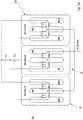
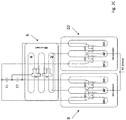
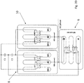
- Figs. 2A-E are schematic diagrams of semiconductor layouts for the T-type phase leg 2 of Fig. 1 . As can be seen in the diagrams of Figs. 2A-E , there are a number of different connection configurations that may be used. It will be appreciated that while the same reference numerals are used throughout Figs. 2A-E to show which components correspond to the internal and external branch modules 6, 8, 10 described above, the configurations shown in these Figs. 2A-E are alternatives to one another.
- Figs. 2C and 2D are particularly advantageous due to their symmetry.
- the configuration of Fig. 2E provides for two AC voltage outputs AC(1), AC(2) that can be connected together externally.
- the connections of the elongate substrates of the internal and external branch modules 6, 8, 10 are shown.
- the internal branch module 6 includes a DC neutral substrate N, and an AC substrate AC.
- the external branch modules 8, 10 include a positive DC rail substrate DC+ connected to the positive DC supply rail 12, and a negative DC rail substrate DC-connected to the negative DC supply rail 14.
- the surrounding area of each of the modules 6, 8, 10 provides a ground connection GD connect. In other examples, the surrounding area may be isolated from the ground, i.e. it may be 'floating'.
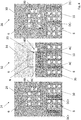
- Figs. 3A and 3B are schematic diagrams of a three-layer DC busbar structure 22 in accordance with an example of the present disclosure. Specifically, Fig. 3A shows a perspective view of the structure 22 and Fig. 3B shows a cross-section of the layers of the structure 22. The individual layers can be seen separately in the exploded view of Fig. 4 , which provides a simplified top-down view of each layer.
- the DC busbar structure 22 is a three-layer structure.
- a first layer 24 contains a positive DC substrate 26 arranged to carry a positive DC voltage. Once constructed, the positive supply rail 12 is connected to the positive DC substrate 26.
- a second layer 28 contains a negative DC substrate 30 arranged to carry a negative DC voltage.
- the negative supply rail 14 is arranged to be connected to the negative DC substrate 30.
- the central layer 32 includes an AC substrate 34 arranged to carry an AC voltage and a DC neutral substrate 36.
- the node 16 between the DC link capacitors C1, C2 in Fig. 1 is connected to the DC neutral substrate 36.
- the nodes 18, 20 are connected to the AC substrate 34.
- Fig. 3A Shown with dotted lines on Fig. 3A are the positions of the connections to the internal branch module 6 and external branch modules 8, 10.
- the layered structure is provided with a number of downhole vias 38 that provide through-layer electrical connections to the substrates below, where these substrates correspond to those shown in Figs. 2A-E .
- the configuration shown in Fig. 2C is in use, though the other configurations may be employed instead by changing the position of the substrates and downhole vias 38 as appropriate.
- Further downhole vias 40 provide for electrical connections to a drive circuit (not shown).
- Fig. 5 is a schematic diagram of a three-phase power converter 42 that uses three phase legs 2a-c.
- Each of the phase legs 2a-c utilises the same layered DC busbar structure described above.
- the layered structure used with the three-phase power converter 42 has the positive, negative, and neutral DC substrates shared between all three phases, i.e. the respective positive and negative supply rails 12, 14 and first node 16 of each phase leg 2a-c are connected to common positive, negative, and neutral DC substrates 26, 30, 36 in the layered DC busbar structure respectively.
- each phase leg 2a-c is provided with its own AC substrate 34.
- each phase leg 2a-c is also connected to a a pair of capacitor units 44a-f that provides the DC link capacitor functionality for the respective phase leg 2a-c, i.e. the pair of capacitor units 44a-f for each phase leg 2a-c provide the function of C1 and C2 as outlined above with respect to Fig. 1 .
- this is optional and these phase legs 2a-c may share one or more capacitors and/or may be provided with multiple capacitors in any combination to provide the capacitance value required.
- the same number of capacitor units are provided above and below the busbar for symmetry.
- capacitor units 44d, 44e are obscured from view (where a further capacitor unit 44f is partially obscured), however these are positioned underneath the busbar, opposite to the corresponding capacity units 44a-c above the busbar, as indicated by the dashed arrows that illustrate their respective positions.
- Fig. 6 is a schematic diagram of two three-phase power converters 42a, 42b connected either side of a common heat sink 46.
- Each of these three-phase power converters 42a, 42b has the same structure as the three-phase power converter 42 of Fig. 5 .
- the first three-phase power converter 42a is arranged on one side 48a of the heat sink 46 while the other three-phase power converter 42b is arranged on the opposite side 48b of the heat sink 46.
- the capacitor units 44a-f can be shared between the six phase legs, i.e. the two sets of three phase legs associated with each of the two three-phase power converters 42a, 42b.
- the actual combination of capacitors used to supply the necessary capacitance value may be selected in accordance with the design requirements.
- Figs 7A-B are schematics diagrams showing a double side cooled heat sink 146 arrangement with connections to a common multi-terminal DC-link capacitor 144.
- two three-phase power converters 142a, 142b are connected either side of the double side cooled heat sink 146.
- the capacitors are all provided in a single capacitor unit 144, which is mounted at the side of the double side cooled heat sink 146 and provided with interconnections 148a, 148b that run alongside, and are connected to, the three-phase power converters 142a, 142b respectively.
- This mounting arrangement is particularly compact because the interconnections 148a, 148b can be electrically connected directly to the appropriate layers of the layered DC busbar structure, without needing any 'bendings' of the conductive paths, as are generally required by conventional arrangements, further improving the parasitic performance compared to such conventional arrangements.
- examples of the present disclosure may provide a compact DC busbar structure for use in the DC link of power converters, e.g. three-level power converters.
- the structure outlined herein may advantageously have improved parasitic parameters (e.g. parasitic inductance) when compared to conventional busbars known in the art per se. While specific examples of the disclosure have been described in detail, it will be appreciated by those skilled in the art that the examples described in detail are not limiting on the scope of the disclosure.
Landscapes
- Engineering & Computer Science (AREA)
- Microelectronics & Electronic Packaging (AREA)
- Power Engineering (AREA)
- Physics & Mathematics (AREA)
- Thermal Sciences (AREA)
- Inverter Devices (AREA)
- Dc-Dc Converters (AREA)
Abstract
Description
- This disclosure relates to a DC link connection bus bar, in particular to a busbar with relatively low inductance, suitable for use in a power converter.
- Generally, electrical applications - including aerospace and vehicular applications - make use of power converters to convert electrical power supplied by a source to a form suitable for onward supply to a load. Many power converters include a DC conversion stage, e.g. AC-DC converters, DC-AC converters, and DC-DC converters. In some such power converters, a 'DC link' connects semiconductor switching devices to electrical energy storage, which in general is provided by one or more capacitors.
- The connecting means between the power switches and the capacitors is usually referred to as a 'DC busbar'. This busbar may also connect the DC conversion stage to an energy source or load. The parasitic parameters (e.g. the parasitic inductance and capacitance) of the DC busbar typically have a direct impact on the performance of the power converter.
- Additionally, it is desirable in many applications (including but not limited to aerospace and vehicular applications) for the DC busbar implementation to be physically compact and light-weight. A smaller, lighter DC busbar may also be beneficial in terms of the amount of material used, and may aid in reducing the parasitic parameter values.
- In power converters that serve a three-phase load, the DC busbar may have three 'phase legs' to supply each phase to the load. Of course, other n-phase arrangements are possible with the appropriate number of phase legs.
- Some DC busbars, known in the art per se, are constructed from a layered (i.e. laminated) in which they are built from parallel layers of a conductive material.
- The busbar of each phase leg of a three-level converter may be provided with four connection substrates - a positive DC substrate, a negative DC substrate, a DC neutral substrate, and an AC substrate. Depending on the type of power converter (e.g. AC-DC or DC-AC), the positive and negative DC substrates may be inputs (i.e. input terminals on these substrates are arranged to take a supply voltage) and the AC substrate may be an output (i.e. an output terminal on this substrate arranged to provide an output voltage) as in a DC-AC converter, or vice versa as in an AC-DC converter (i.e. an AC input and a DC output). The DC neutral substrate provides a current return path.
- In accordance with a first aspect, the present disclosure provides a layered DC busbar structure comprising:
- a positive DC substrate arranged to carry a positive DC voltage, said positive DC substrate being arranged on a first layer;
- a negative DC substrate arranged to carry a negative DC voltage, said negative DC substrate being arranged on a second layer;
- a DC neutral substrate arranged on a central layer between said first and second layers; and
- an AC substrate arranged to carry an AC voltage, said AC substrate being arranged on the central layer and substantially coplanar with the DC neutral substrate.
- Thus it will be appreciated by those skilled in the art that examples of the present disclosure provide an improved DC busbar structure in which the DC neutral substrate and the AC substrate share a common layer, 'sandwiched' between the positive and negative DC substrates. This three-layer structure may help to minimise the parasitic inductance associate with the DC busbar, which may provide improvements in the performance of the busbar. In particular, this configuration may advantageously provide for a symmetric coupling of the DC neutral and AC layers to the positive and negative DC layers, with negligible coupling between the DC neutral and AC layers.
- Furthermore, the layered DC busbar may have a reduced physical size and volume compared to conventional structures, which may provide significant improvements in the power density of the DC link in the power converter. Examples of the present disclosure may be particularly suitable for three-level power converters in applications requiring high power levels, e.g. power levels of hundreds of kilowatts and greater. The compactness of the layered DC busbar disclosed herein is facilitated by reducing the number of layers with respect to the number of terminals when compared to conventional approaches.
- A further advantage afforded by examples of the present disclosure is that the layered structure may be readily extended to provide multiple phase legs. It has been appreciated that the positive DC substrate, negative DC substrate, and/or DC neutral substrate - and preferably all three of these - may be shared between multiple phase legs, where a separate AC substrate is provided for each phase leg. Thus, in some examples, the layered DC busbar comprises a plurality of AC substrates, each arranged to carry a respective AC voltage, wherein each AC substrate is arranged on the central layer and substantially coplanar with the DC neutral substrate. Thus the compact structure of the layered DC busbar provided in the present disclosure may be extended to multiple phase legs simply by adding further AC substrates in the central layer.
- The central layer may be seen as being divided into two halves, where the DC neutral substrate occupies one half, and the AC substrate occupies the other half, where a gap is provided between these halves, this gap providing isolation between the DC neutral and AC substrates. It will be appreciated that these 'halves' may not necessarily be equal in size. Where multiple AC substrates are provided, these may together occupy the half of the central layer not occupied by the DC neutral substrate. The positive and negative DC substrates may, by contrast, occupy the full extent of their respective layers. Thus, in some examples, the positive and negative DC substrates substantially fully cover the central layer.
- The first aspect of the disclosure extends to a power converter comprising a DC link, wherein the DC link comprises a layered DC busbar structure comprising:
- a positive DC substrate arranged to carry a positive DC voltage, said positive DC substrate being arranged on a first layer;
- a negative DC substrate arranged to carry a negative DC voltage, said negative DC substrate being arranged on a second layer;
- a DC neutral substrate arranged on a central layer between said first and second layers; and
- an AC substrate arranged to carry an AC voltage, said AC substrate being arranged on the central layer and substantially coplanar with the DC neutral substrate.
- While the layered DC busbar structure may be useful for a number of different power converters, in some examples, the layered DC busbar structure is used for a three-level power converter, and in some examples it is used to provide a connection means for a 'T-type' three-level power converter.
- In some examples, the power converter comprises:
- a DC voltage supply connected between a positive DC supply rail and a negative DC supply rail, wherein the positive DC supply rail is connected to the positive DC substrate, and wherein the negative DC supply rail is connected to the negative DC substrate;
- a first capacitor and a second capacitor connected in series between said positive and negative DC supply rails, said first and second capacitors being connected at a first node therebetween, wherein the first node is connected to the DC neutral substrate;
- an internal branch module comprising a first switching arrangement connected between the first node and a second node, wherein the second node is connected to the AC substrate; and
- an external branch module comprising a second switching arrangement, said second switching arrangement comprising first and second switches connected in series at the second node.
- Generally, an AC circuit will be connected to the output of the power converter, i.e. at the second node. Thus in a set of examples, an external AC circuit is connected to the second node, optionally wherein the external circuit comprises an inductor connected to the second node. This inductor may be a discrete inductor, or may be the intrinsic inductance of, for example, a cable or an electrical machine connected to the output of the power converter.
- A potentially overlapping set of examples is envisaged in which a plurality, for example two, DC voltage supplies are arranged in series between the positive and negative DC supply rails, wherein a common point between said plurality of DC voltage supplies is connected to the DC neutral substrate.
- In a set of examples, the power converter comprises a second external branch module comprising a third switching arrangement, said second switching arrangement comprising first and second switches connected in series at the second node.
- The first and second switches of each external branch module may be connected between the positive and negative DC supply rails, wherein the first switch is connected between the positive DC supply rail and the second node, and the second switch is connected between the second node and the negative DC supply rail.
- The layered DC busbar may, in some examples, comprise a plurality of vias that provide electrical connections between the substrates, the rails, the nodes, and/or the switches of the power converter as appropriate. The layered DC busbar may, in some potentially overlapping examples, comprise further vias to provide for electrical connections to a drive circuit.
- Beneficially, the first and second capacitors (or 'DC link' capacitors) can be mounted directly on the layered substrates and be provided with the necessary electrical connections to the appropriate layers directly so as to provide DC link functionality. This may also provide for a compact arrangement in which the DC link capacitors can be 'flush mounted' on the DC busbar, rather than being connected at an angle (e.g. perpendicular to) the DC busbar with connectors (or electrical 'bridges') to provide for connections to the rest of the circuit as in conventional arrangements known in the art per se.
- Bendings, such as those used in conventional arrangements, increase the parasitic inductance because, depending on busbar characteristics like thickness and constructive factors, they may require increasing the distance between conducting layers. Bendings in the conductive paths also imply an asymmetry in the mutual coupling between those paths. Conversely, the improved connection with a shorter distance and no busbar bendings may advantageously lead to smaller parasitic parameters, especially parasitic inductance. This may translate into a smooth, safe transient commutation for the power semiconductors.
- In some examples, the internal branch module may comprise first and second elongate substrates aligned along a first axis, said first elongate substrate being connected to the first node and said second elongate substrate being connected to the second node. The internal branch module can therefore be aligned such that it can be provided with connections to the AC and DC neutral substrates, i.e. it can 'straddle' the two halves of the central layer.
- In some potentially overlapping examples, the, or each, external branch module may comprise first, second, and third elongate substrates aligned along a second axis, wherein the first elongate substrate is connected to the positive DC supply rail, the second elongate substrate is connected to the negative DC supply rail, and the third elongate substrate is connected to the second node.
- In some examples in which two external branch modules are provided, the external branch modules may be placed side by side such that the current conductive path to the internal branch module is symmetrical, which may benefit the dynamic current sharing during the commutation transient. In addition, the close proximity of the modules may benefit the gate driver circuit because the smaller distances may further reduce the parasitic parameters associated with the gate circuit. This combined with a good symmetric circuit may also improve the dynamic current sharing.
- In a set of examples, the first and second axes are substantially perpendicular to each other. This may provide for a compact layout, particularly in examples where the central layer is divided into halves as outlined above.
- The power converter may comprise a heat sink. In a set of examples, the power converter comprises two layered DC busbars as outlined above, wherein the first layered DC busbar is positioned on a first side of the heat sink and the second DC busbar is positioned on a second side of the heat sink, opposite to said first side. The DC capacitors may then be shared between the DC busbars. This configuration has the clear benefit of a smaller size enabling considerably higher power densities than conventional configurations by requiring only one heat sink instead of two for the two DC busbars. An additional advantage is that the arrangement can be configured to connect the two sets of phase legs (i.e. the phase legs associated with each of the two DC busbars) with reduced parasitic parameters. This may enable improved operation of the complete power converter with a reduction in undesired interactions between the phase leg branches.
- In accordance with such examples, the DC link can be arranged as a common DC link, i.e. in which its parts are connected through a low inductance path; or it can be arranged as two DC links forming part of separate circuits. Alternatively, even if they are part of the same circuit, they may be connected through a large impedance. In case of a common DC link, the capacitors may be integrated to a low inductance conductive structure that connects the various capacitor terminals among them and to the power modules.
- Certain examples of the present disclosure will now be described with reference to the accompanying drawings, in which:
-
Fig. 1 is a circuit diagram of a T-type phase leg of a three-level power converter; -
Figs. 2A-E are schematic diagrams of semiconductor layouts for the T-type phase leg ofFig. 1 ; -
Figs. 3A-B are schematic diagrams of a three-layer DC busbar structure in accordance with an example of the present disclosure; -
Fig. 4 is a schematic diagram providing an exploded view of the layers ofFigs. 3A-B ; -
Fig. 5 is a schematic diagram of a three-phase power converter that uses three phase legs side-by-side; -
Fig. 6 is a schematic diagram of two three-phase power converters connected either side of a common heat sink; and -
Figs 7A-B are schematics diagrams showing a double side cooled heat sink arrangement with connections to a common multi-terminal DC-link capacitor. -
Fig. 1 is a circuit diagram of a T-type phase leg 2 of a three-level power converter. Thephase leg 2 includes aDC voltage source 4, aninternal branch module 6, and twoexternal branch modules DC power source 4 is connected between a positiveDC supply rail 12 and a negativeDC supply rail 14. - The
internal branch module 6 andexternal branch modules - A pair of DC link capacitors C1, C2 are connected in series between the DC supply rails 12, 14, and are connected at a
first node 16. These capacitors C1, C2 serve to smooth the DC voltage output of theDC voltage source 4. The DC link capacitors C1, C2 also protect upstream circuits from the transient response of downstream circuits. Typically, the DC link capacitor values are selected to optimise the stability of the DC voltage across the bus. - The
first node 16 between the capacitors C1, C2 is connected to asecond node 18 via theinternal branch module 6, which is constructed from a pair of transistors T2, T3 arranged in series. - The first
external branch module 8 is constructed from a pair of transistors T1a, T4a connected in series, where the transistors T1a, T4a are connected at thesecond node 18. Similarly, the secondexternal branch module 10 is constructed from a pair of transistors T1b, T4b connected in series, where the transistors T1b, T4b are connected at anode 20, which is connected to thesecond node 18. Thus, effectively, the pair of transistors T1b, T4b are connected at thesecond node 18. - A first terminal of an inductor L1 is connected to the
nodes external branch modules nodes -
Figs. 2A-E are schematic diagrams of semiconductor layouts for the T-type phase leg 2 ofFig. 1 . As can be seen in the diagrams ofFigs. 2A-E , there are a number of different connection configurations that may be used. It will be appreciated that while the same reference numerals are used throughoutFigs. 2A-E to show which components correspond to the internal andexternal branch modules Figs. 2A-E are alternatives to one another. - The configurations shown in
Figs. 2C and2D are particularly advantageous due to their symmetry. The configuration ofFig. 2E provides for two AC voltage outputs AC(1), AC(2) that can be connected together externally. - In each of the configurations shown, the connections of the elongate substrates of the internal and
external branch modules internal branch module 6 includes a DC neutral substrate N, and an AC substrate AC. Theexternal branch modules DC supply rail 12, and a negative DC rail substrate DC-connected to the negativeDC supply rail 14. The surrounding area of each of themodules -
Figs. 3A and3B are schematic diagrams of a three-layerDC busbar structure 22 in accordance with an example of the present disclosure. Specifically,Fig. 3A shows a perspective view of thestructure 22 andFig. 3B shows a cross-section of the layers of thestructure 22. The individual layers can be seen separately in the exploded view ofFig. 4 , which provides a simplified top-down view of each layer. - As can be seen in
Figs. 3A and3B , theDC busbar structure 22 is a three-layer structure. Afirst layer 24 contains apositive DC substrate 26 arranged to carry a positive DC voltage. Once constructed, thepositive supply rail 12 is connected to thepositive DC substrate 26. - A
second layer 28 contains anegative DC substrate 30 arranged to carry a negative DC voltage. Thenegative supply rail 14 is arranged to be connected to thenegative DC substrate 30. - Between the
layers negative DC substrates central layer 32, where the AC and DCneutral substrates gap 33 between them. Thecentral layer 32 includes anAC substrate 34 arranged to carry an AC voltage and a DCneutral substrate 36. Specifically, thenode 16 between the DC link capacitors C1, C2 inFig. 1 is connected to the DCneutral substrate 36. Thenodes AC substrate 34. - Shown with dotted lines on
Fig. 3A are the positions of the connections to theinternal branch module 6 andexternal branch modules downhole vias 38 that provide through-layer electrical connections to the substrates below, where these substrates correspond to those shown inFigs. 2A-E . In the example shown inFig. 3A , the configuration shown inFig. 2C is in use, though the other configurations may be employed instead by changing the position of the substrates anddownhole vias 38 as appropriate. Furtherdownhole vias 40 provide for electrical connections to a drive circuit (not shown). - With reference to the exploded view of
Fig. 4 , the connections between the substrates of thephase leg 2 and the substrates of the layeredDC busbar 22 can be seen. -
Fig. 5 is a schematic diagram of a three-phase power converter 42 that uses threephase legs 2a-c. Each of thephase legs 2a-c utilises the same layered DC busbar structure described above. With respect to the DC busbar, the layered structure used with the three-phase power converter 42 has the positive, negative, and neutral DC substrates shared between all three phases, i.e. the respective positive andnegative supply rails first node 16 of eachphase leg 2a-c are connected to common positive, negative, andneutral DC substrates phase leg 2a-c is provided with itsown AC substrate 34. - In this example, each
phase leg 2a-c is also connected to a a pair ofcapacitor units 44a-f that provides the DC link capacitor functionality for therespective phase leg 2a-c, i.e. the pair ofcapacitor units 44a-f for eachphase leg 2a-c provide the function of C1 and C2 as outlined above with respect toFig. 1 . However, this is optional and thesephase legs 2a-c may share one or more capacitors and/or may be provided with multiple capacitors in any combination to provide the capacitance value required. Generally, the same number of capacitor units are provided above and below the busbar for symmetry. InFig. 5 , two of thecapacitor units further capacitor unit 44f is partially obscured), however these are positioned underneath the busbar, opposite to thecorresponding capacity units 44a-c above the busbar, as indicated by the dashed arrows that illustrate their respective positions. -
Fig. 6 is a schematic diagram of two three-phase power converters common heat sink 46. Each of these three-phase power converters phase power converter 42 ofFig. 5 . The first three-phase power converter 42a is arranged on one side 48a of theheat sink 46 while the other three-phase power converter 42b is arranged on theopposite side 48b of theheat sink 46. - In this arrangement, the
capacitor units 44a-f can be shared between the six phase legs, i.e. the two sets of three phase legs associated with each of the two three-phase power converters -
Figs 7A-B are schematics diagrams showing a double side cooledheat sink 146 arrangement with connections to a common multi-terminal DC-link capacitor 144. As inFig. 6 , two three-phase power converters heat sink 146. In this arrangement, the capacitors are all provided in asingle capacitor unit 144, which is mounted at the side of the double side cooledheat sink 146 and provided withinterconnections phase power converters interconnections - Thus examples of the present disclosure may provide a compact DC busbar structure for use in the DC link of power converters, e.g. three-level power converters. The structure outlined herein may advantageously have improved parasitic parameters (e.g. parasitic inductance) when compared to conventional busbars known in the art per se. While specific examples of the disclosure have been described in detail, it will be appreciated by those skilled in the art that the examples described in detail are not limiting on the scope of the disclosure.
Claims (13)
- A layered DC busbar structure comprising:a positive DC substrate arranged to carry a positive DC voltage, said positive DC substrate being arranged on a first layer;a negative DC substrate arranged to carry a negative DC voltage, said negative DC substrate being arranged on a second layer;a DC neutral substrate arranged on a central layer between said first and second layers; andan AC substrate arranged to carry an AC voltage, said AC substrate being arranged on the central layer and substantially coplanar with the DC neutral substrate.
- The layered DC busbar structure as claimed in claim 1, further comprising a plurality of AC substrates, each arranged to carry a respective AC voltage, wherein each AC substrate is arranged on the central layer and substantially coplanar with the DC neutral substrate.
- The layered DC busbar structure as claimed in claim 1 or 2, wherein the positive and negative DC substrates substantially fully cover the central layer.
- The layered DC busbar structure as claimed in any preceding claim, further comprising a plurality of vias that provide electrical connections between the substrates and the rails and nodes of an external power converter.
- The layered DC busbar structure as claimed in any preceding claim, further comprising vias to provide for electrical connections to an external drive circuit.
- A power converter comprising a DC link, wherein the DC link comprises a layered DC busbar structure as claimed in any of claims 1 to 5.
- The power converter as claimed in claim 6, further comprising:a DC voltage supply connected between a positive DC supply rail and a negative DC supply rail, wherein the positive DC supply rail is connected to the positive DC substrate, and wherein the negative DC supply rail is connected to the negative DC substrate;a first capacitor and a second capacitor connected in series between said positive and negative DC supply rails, said first and second capacitors being connected at a first node therebetween, wherein the first node is connected to the DC neutral substrate;an internal branch module comprising a first switching arrangement connected between the first node and a second node, wherein the second node is connected to the AC substrate; andan external branch module comprising a second switching arrangement, said second switching arrangement comprising first and second switches connected in series at the second node.
- The power converter as claimed in claim 7, wherein the power converter comprises an external AC circuit is connected to the second node, optionally wherein the external circuit comprises an inductor connected to the second node.
- The power converter as claimed in claim 7 or 8, wherein the first and second capacitors are mounted directly on the layered substrates.
- The power converter as claimed in any of claims 7 to 9, further comprising a second external branch module comprising a third switching arrangement, said second switching arrangement comprising first and second switches connected in series at the second node, optionally wherein the external branch modules are placed side by side.
- The power converter as claimed in any of claims 7 to 10, wherein the internal branch module comprises first and second elongate substrates aligned along a first axis, said first elongate substrate being connected to the first node and said second elongate substrate being connected to the second node.
- The power converter as claimed in any of claims 7 to 11, wherein the, or each, external branch module may comprise first, second, and third elongate substrates aligned along a second axis, wherein the first elongate substrate is connected to the positive DC supply rail, the second elongate substrate is connected to the negative DC supply rail, and the third elongate substrate is connected to the second node.
- The power converter as claimed in any of claims 6 to 12, further comprising a heat sink and a further layered DC busbar, wherein the first layered DC busbar is positioned on a first side of the heat sink and the second DC busbar is positioned on a second side of the heat sink, opposite to said first side.
Applications Claiming Priority (1)
| Application Number | Priority Date | Filing Date | Title |
|---|---|---|---|
| US16/821,210 US11108336B1 (en) | 2020-03-17 | 2020-03-17 | Power converter |
Publications (1)
| Publication Number | Publication Date |
|---|---|
| EP3883114A1 true EP3883114A1 (en) | 2021-09-22 |
Family
ID=74187208
Family Applications (1)
| Application Number | Title | Priority Date | Filing Date |
|---|---|---|---|
| EP21152174.5A Withdrawn EP3883114A1 (en) | 2020-03-17 | 2021-01-18 | Power converter |
Country Status (2)
| Country | Link |
|---|---|
| US (1) | US11108336B1 (en) |
| EP (1) | EP3883114A1 (en) |
Families Citing this family (4)
| Publication number | Priority date | Publication date | Assignee | Title |
|---|---|---|---|---|
| DE102019202777A1 (en) * | 2018-12-18 | 2020-06-18 | Robert Bosch Gmbh | Low inductance connector |
| EP3893615B1 (en) * | 2020-04-07 | 2024-10-02 | Hamilton Sundstrand Corporation | Power converter assemblies with busbars |
| DE102020133622A1 (en) * | 2020-12-15 | 2022-06-15 | Danfoss Power Electronics A/S | Heatsink arrangement for a power converter |
| DE102024203650A1 (en) * | 2024-04-19 | 2025-10-23 | Robert Bosch Gesellschaft mit beschränkter Haftung | Inverter unit |
Citations (5)
| Publication number | Priority date | Publication date | Assignee | Title |
|---|---|---|---|---|
| US20120205983A1 (en) * | 2009-11-17 | 2012-08-16 | Toshiba Mitsubishi-Electric Industrial Systems Corporation | Three-level power conversion apparatus |
| US20130187453A1 (en) * | 2011-11-22 | 2013-07-25 | Quantum Fuel Systems Technologies Worldwide Inc. | Fishtail Packaging and Cooling |
| CN207098959U (en) * | 2017-09-07 | 2018-03-13 | 中车永济电机有限公司 | Water cooling substrate and the integrated auxiliary power module of commutation inversion |
| CN207304393U (en) * | 2017-09-07 | 2018-05-01 | 中车永济电机有限公司 | Rectification and the auxiliary converter power cell and composite bus bar of inversion facilitation |
| US20180183350A1 (en) * | 2016-12-22 | 2018-06-28 | Fuji Electric Co., Ltd. | Power conversion device |
Family Cites Families (17)
| Publication number | Priority date | Publication date | Assignee | Title |
|---|---|---|---|---|
| FR2684250B1 (en) * | 1991-11-27 | 1994-04-01 | Merlin Gerin | HIGH QUALITY ELECTRICAL ENERGY DISTRIBUTION SYSTEM. |
| US6822850B2 (en) * | 2002-09-27 | 2004-11-23 | Rockwell Automation Technologies, Inc. | Laminated bus bar for use with a power conversion configuration |
| GB0226714D0 (en) | 2002-11-15 | 2002-12-24 | Bombardier Transp Gmbh | Converter module |
| US8947899B2 (en) * | 2012-03-09 | 2015-02-03 | Rockwell Automation Technologies, Inc. | Split laminated DC bus structure |
| CN103368359B (en) * | 2012-04-11 | 2016-04-13 | 台达电子工业股份有限公司 | Converter power unit and its busbar |
| US8942020B2 (en) | 2012-06-22 | 2015-01-27 | General Electric Company | Three-level phase leg for a power converter |
| CN102882385B (en) | 2012-10-22 | 2015-09-23 | 台达电子工业股份有限公司 | Laminated busbar structure for three-level power converter and power converter |
| US9270102B2 (en) * | 2013-07-30 | 2016-02-23 | Ford Global Technologies, Inc. | Multilayered bus bar |
| CN105450042B (en) * | 2014-09-26 | 2018-04-17 | 台达电子工业股份有限公司 | Three-level power converter and its power unit |
| EP3145286B1 (en) | 2015-09-15 | 2019-05-01 | ABB Schweiz AG | Heat dissipation in power electronic assemblies |
| US10027251B2 (en) | 2016-01-05 | 2018-07-17 | Atse, Llc | Power converter |
| US10103534B2 (en) * | 2016-10-27 | 2018-10-16 | General Electric Company | Low inductance busbar systems and methods |
| GB2559180B (en) | 2017-01-30 | 2020-09-09 | Yasa Ltd | Semiconductor cooling arrangement |
| DE112017008003B4 (en) * | 2017-08-30 | 2025-03-13 | Mitsubishi Electric Corporation | MAIN CIRCUIT WIRING LINK AND POWER CONVERSION DEVICE |
| US10720378B2 (en) | 2017-08-31 | 2020-07-21 | Delta Electronics (Shanghai) Co., Ltd | Component structure, power module and power module assembly structure |
| US11332087B2 (en) | 2018-06-04 | 2022-05-17 | Westinghouse Air Brake Technologies Corporation | Phase module assembly of a multi-phase inverter |
| US10701795B2 (en) * | 2018-09-11 | 2020-06-30 | Ge Aviation Systems Llc | Direct current link bus for a power converter and method of forming a direct current link bus |
-
2020
- 2020-03-17 US US16/821,210 patent/US11108336B1/en active Active
-
2021
- 2021-01-18 EP EP21152174.5A patent/EP3883114A1/en not_active Withdrawn
Patent Citations (5)
| Publication number | Priority date | Publication date | Assignee | Title |
|---|---|---|---|---|
| US20120205983A1 (en) * | 2009-11-17 | 2012-08-16 | Toshiba Mitsubishi-Electric Industrial Systems Corporation | Three-level power conversion apparatus |
| US20130187453A1 (en) * | 2011-11-22 | 2013-07-25 | Quantum Fuel Systems Technologies Worldwide Inc. | Fishtail Packaging and Cooling |
| US20180183350A1 (en) * | 2016-12-22 | 2018-06-28 | Fuji Electric Co., Ltd. | Power conversion device |
| CN207098959U (en) * | 2017-09-07 | 2018-03-13 | 中车永济电机有限公司 | Water cooling substrate and the integrated auxiliary power module of commutation inversion |
| CN207304393U (en) * | 2017-09-07 | 2018-05-01 | 中车永济电机有限公司 | Rectification and the auxiliary converter power cell and composite bus bar of inversion facilitation |
Also Published As
| Publication number | Publication date |
|---|---|
| US20210297002A1 (en) | 2021-09-23 |
| US11108336B1 (en) | 2021-08-31 |
Similar Documents
| Publication | Publication Date | Title |
|---|---|---|
| US11108336B1 (en) | Power converter | |
| US12051980B2 (en) | Variable inverter/rectifier/transformer | |
| US9350269B2 (en) | Configurable hybrid converter circuit | |
| US9143049B2 (en) | Three-level power conversion apparatus | |
| US20100328833A1 (en) | Power module with additional transient current path and power module system | |
| US11791628B2 (en) | SST system with multiple LVDC outputs | |
| WO2007113979A1 (en) | Power converter and its assembling method | |
| US11791741B2 (en) | Power converter assemblies with busbars | |
| Xiang et al. | Resonant modular multilevel DC–DC converters for both high and low step-ratio connections in MVDC distribution systems | |
| JP6804326B2 (en) | Power converters, photovoltaic power conditioner systems, power storage systems, non-disruptive power supply systems, wind power generation systems, and motor drive systems | |
| JP2015065727A (en) | Insulation power supply device | |
| WO2014021112A1 (en) | Switching element unit | |
| CN215222037U (en) | Bus connection device, NPC three-level power module and NPC three-level converter | |
| CN108631637B (en) | Switched mode power converter configured to control at least one phase of a polyphase electrical receiver having at least three phases | |
| US7619325B1 (en) | Ring configuration for compact power supply of power electronics | |
| KR20240021120A (en) | Method and circuit for an integrated dc-dc converter in an ac battery | |
| JP2017055610A (en) | Power semiconductor device | |
| KR102831477B1 (en) | Integrated power module | |
| KR20220061989A (en) | Modular Switching Cell | |
| US10541625B2 (en) | Power conversion device | |
| US12395095B2 (en) | Commutation cell, flying capacitor module and multilevel converter | |
| JP7086308B2 (en) | DC / DC converter device | |
| JP7500508B2 (en) | Power Conversion Equipment | |
| Guépratte et al. | Fault tolerance on interleaved inverter with magnetic couplers | |
| US20250175071A1 (en) | Field configurable array of power processing blocks |
Legal Events
| Date | Code | Title | Description |
|---|---|---|---|
| PUAI | Public reference made under article 153(3) epc to a published international application that has entered the european phase |
Free format text: ORIGINAL CODE: 0009012 |
|
| STAA | Information on the status of an ep patent application or granted ep patent |
Free format text: STATUS: THE APPLICATION HAS BEEN PUBLISHED |
|
| AK | Designated contracting states |
Kind code of ref document: A1 Designated state(s): AL AT BE BG CH CY CZ DE DK EE ES FI FR GB GR HR HU IE IS IT LI LT LU LV MC MK MT NL NO PL PT RO RS SE SI SK SM TR |
|
| STAA | Information on the status of an ep patent application or granted ep patent |
Free format text: STATUS: REQUEST FOR EXAMINATION WAS MADE |
|
| 17P | Request for examination filed |
Effective date: 20220322 |
|
| RBV | Designated contracting states (corrected) |
Designated state(s): AL AT BE BG CH CY CZ DE DK EE ES FI FR GB GR HR HU IE IS IT LI LT LU LV MC MK MT NL NO PL PT RO RS SE SI SK SM TR |
|
| STAA | Information on the status of an ep patent application or granted ep patent |
Free format text: STATUS: EXAMINATION IS IN PROGRESS |
|
| 17Q | First examination report despatched |
Effective date: 20221104 |
|
| STAA | Information on the status of an ep patent application or granted ep patent |
Free format text: STATUS: THE APPLICATION IS DEEMED TO BE WITHDRAWN |
|
| 18D | Application deemed to be withdrawn |
Effective date: 20230516 |