EP3883110A1 - Digital control circuit, charge pump circuit and controlling method thereof - Google Patents
Digital control circuit, charge pump circuit and controlling method thereof Download PDFInfo
- Publication number
- EP3883110A1 EP3883110A1 EP21173565.9A EP21173565A EP3883110A1 EP 3883110 A1 EP3883110 A1 EP 3883110A1 EP 21173565 A EP21173565 A EP 21173565A EP 3883110 A1 EP3883110 A1 EP 3883110A1
- Authority
- EP
- European Patent Office
- Prior art keywords
- voltage
- output voltage
- charge pump
- mode
- pump circuit
- Prior art date
- Legal status (The legal status is an assumption and is not a legal conclusion. Google has not performed a legal analysis and makes no representation as to the accuracy of the status listed.)
- Granted
Links
Images



Classifications
-
- H—ELECTRICITY
- H02—GENERATION; CONVERSION OR DISTRIBUTION OF ELECTRIC POWER
- H02M—APPARATUS FOR CONVERSION BETWEEN AC AND AC, BETWEEN AC AND DC, OR BETWEEN DC AND DC, AND FOR USE WITH MAINS OR SIMILAR POWER SUPPLY SYSTEMS; CONVERSION OF DC OR AC INPUT POWER INTO SURGE OUTPUT POWER; CONTROL OR REGULATION THEREOF
- H02M3/00—Conversion of DC power input into DC power output
- H02M3/02—Conversion of DC power input into DC power output without intermediate conversion into AC
- H02M3/04—Conversion of DC power input into DC power output without intermediate conversion into AC by static converters
- H02M3/06—Conversion of DC power input into DC power output without intermediate conversion into AC by static converters using resistors or capacitors, e.g. potential divider
- H02M3/07—Conversion of DC power input into DC power output without intermediate conversion into AC by static converters using resistors or capacitors, e.g. potential divider using capacitors charged and discharged alternately by semiconductor devices with control electrode, e.g. charge pumps
-
- H—ELECTRICITY
- H02—GENERATION; CONVERSION OR DISTRIBUTION OF ELECTRIC POWER
- H02M—APPARATUS FOR CONVERSION BETWEEN AC AND AC, BETWEEN AC AND DC, OR BETWEEN DC AND DC, AND FOR USE WITH MAINS OR SIMILAR POWER SUPPLY SYSTEMS; CONVERSION OF DC OR AC INPUT POWER INTO SURGE OUTPUT POWER; CONTROL OR REGULATION THEREOF
- H02M1/00—Details of apparatus for conversion
- H02M1/08—Circuits specially adapted for the generation of control voltages for semiconductor devices incorporated in static converters
-
- H—ELECTRICITY
- H02—GENERATION; CONVERSION OR DISTRIBUTION OF ELECTRIC POWER
- H02M—APPARATUS FOR CONVERSION BETWEEN AC AND AC, BETWEEN AC AND DC, OR BETWEEN DC AND DC, AND FOR USE WITH MAINS OR SIMILAR POWER SUPPLY SYSTEMS; CONVERSION OF DC OR AC INPUT POWER INTO SURGE OUTPUT POWER; CONTROL OR REGULATION THEREOF
- H02M1/00—Details of apparatus for conversion
- H02M1/36—Means for starting or stopping converters
-
- H—ELECTRICITY
- H03—ELECTRONIC CIRCUITRY
- H03F—AMPLIFIERS
- H03F1/00—Details of amplifiers with only discharge tubes, only semiconductor devices or only unspecified devices as amplifying elements
- H03F1/02—Modifications of amplifiers to raise the efficiency, e.g. gliding Class A stages, use of an auxiliary oscillation
-
- H—ELECTRICITY
- H03—ELECTRONIC CIRCUITRY
- H03F—AMPLIFIERS
- H03F1/00—Details of amplifiers with only discharge tubes, only semiconductor devices or only unspecified devices as amplifying elements
- H03F1/02—Modifications of amplifiers to raise the efficiency, e.g. gliding Class A stages, use of an auxiliary oscillation
- H03F1/0205—Modifications of amplifiers to raise the efficiency, e.g. gliding Class A stages, use of an auxiliary oscillation in transistor amplifiers
- H03F1/0211—Modifications of amplifiers to raise the efficiency, e.g. gliding Class A stages, use of an auxiliary oscillation in transistor amplifiers with control of the supply voltage or current
-
- H—ELECTRICITY
- H03—ELECTRONIC CIRCUITRY
- H03F—AMPLIFIERS
- H03F1/00—Details of amplifiers with only discharge tubes, only semiconductor devices or only unspecified devices as amplifying elements
- H03F1/30—Modifications of amplifiers to reduce influence of variations of temperature or supply voltage or other physical parameters
- H03F1/305—Modifications of amplifiers to reduce influence of variations of temperature or supply voltage or other physical parameters in case of switching on or off of a power supply
-
- H—ELECTRICITY
- H03—ELECTRONIC CIRCUITRY
- H03F—AMPLIFIERS
- H03F3/00—Amplifiers with only discharge tubes or only semiconductor devices as amplifying elements
- H03F3/20—Power amplifiers, e.g. Class B amplifiers, Class C amplifiers
Definitions
- the present application relates to a charge pump circuit and controlling method thereof, and more particularly, to a charge pump circuit and controlling method thereof capable of reducing inrush currents generated when transforming among voltage modes.
- FIG. 1 is a structural diagram of a conventional class-G amplifier circuit 10 with a digital input.
- the conventional class-G amplifier circuit 10 includes a digital front end circuit 102, a digital-to-analog converter (DAC) 104, a class-AB amplifier 106, a charge-pump control logic circuit 108 and a charge pump circuit 110.
- the charge-pump control logic circuit 108 adjusts an output voltage of the charge pump circuit 110 according to an input signal, such that the charge pump circuit 110 may transform among different voltage modes.
- the conventional charge pump circuit 110 Before the conventional charge pump circuit 110 is transformed from a 1/3VDD mode to a VDD mode, the conventional charge pump circuit 110 enters a soft ramp-up mode, an output voltage of the charge pump circuit 110 is charged by a smaller fixed current. After the charge pump circuit 110 is charged for a fixed time period, the charge pump circuit 110 enters the VDD mode. When the charge pump circuit 110 is transformed from the VDD mode to the 1/3VDD mode, a three-phase soft switching is utilized for transforming the output voltage to the 1/3VDD mode. However, a charging time period of the conventional charge pump circuit 110 is fixed during the soft ramp-up mode.
- the charge pump circuit 110 enters the VDD mode and huge inrush currents are generated, which causes distortions when the class-G amplifier circuit is applied on the audio and generates pop noises.
- the charging period is too long, a ramp-up process of the output voltage is too slow and causes clipping of the output voltage of the class-G amplifier circuit and distortions.
- the charging time of the output voltage of the charge pump circuit 100 is easily affected by an output device and loading current, which makes digital control logic of the class-G amplifier circuit difficult.
- a time period needed for the transformation to the 1/3VDD is directly related to the loading current and output capacitors. When the time period is too short, the output voltage of the charge pump circuit 100 cannot be reduced to the 1/3VDD mode. In contrast, if the time period is too long, the output voltage is lower than 1/3VDD due to a huge impedance caused by the soft switching of the charge pump circuit 100, which generates huge inrush currents.
- the present application provides a digital control circuit, configured to receive a up digital signal and a down digital signal, and adjust a first output voltage to a voltage level of an input voltage and adjust an second output voltage to a ground voltage level according to the up digital signal and the down digital signal, comprises a digital-to-analog converter (DAC), configured to generate a corresponding up reference voltage and a corresponding down reference voltage according to the up digital signal and the down digital signal; and a voltage follower, comprising a plurality of operational amplifiers and a plurality of transistor switches, configured to lock the first output voltage and the second output voltage according to the up reference voltage and the down reference voltage; wherein the up digital signal and the down digital signal are varied with time.
- DAC digital-to-analog converter
- An embodiment of the present application provides a charge pump circuit, comprises a digital control circuit, coupled to a switch module of the charge pump, configured to receive a up digital signal and a down digital signal, and adjust a first output voltage to a voltage level of an input voltage and adjust an second output voltage to a ground voltage level according to the up digital signal and the down digital signal, comprises a digital-to-analog converter (DAC), configured to generate a corresponding up reference voltage and a corresponding down reference voltage according to the up digital signal and the down digital signal; and a voltage follower, comprising a plurality of operational amplifiers and a plurality of transistor switches, configured to lock the first output voltage and the second output voltage according to the up reference voltage and the down reference voltage.
- DAC digital-to-analog converter
- the charge pump circuit further comprises a balance release circuit, coupled to the digital control circuit and the switch module, configured to maintain a common mode voltage of the first output voltage and the second output voltage at a fixed value through a common mode feedback loop, when the first output voltage and the second output voltage is discharging or charging; wherein the common mode voltage is half of the input voltage; wherein the common mode feedback loop includes a plurality of operational amplifiers and a plurality of resistors.
- a balance release circuit coupled to the digital control circuit and the switch module, configured to maintain a common mode voltage of the first output voltage and the second output voltage at a fixed value through a common mode feedback loop, when the first output voltage and the second output voltage is discharging or charging; wherein the common mode voltage is half of the input voltage; wherein the common mode feedback loop includes a plurality of operational amplifiers and a plurality of resistors.
- the switch module comprises a plurality of switches, a plurality of output capacitors, a loading resistor and a soft ramp-up switch, and is configured to generate the first output voltage and the second output voltage according to the input voltage and control the plurality of switches and the soft ramp-up switch to transform the first output voltage and the second output voltage with a first mode, a ramp-up mode, a second mode and a balance release mode.
- the first output voltage is adjusted to the voltage level of the input voltage according to the up reference voltage and the second output voltage is adjusted to the ground voltage level according to the down reference voltage.
- the plurality of transistor switches of the digital control circuit are turned on to connect the input voltage and the ground voltage level to enter the second mode.
- the first output voltage and the second output voltage are only related to the up reference voltage and the down reference voltage.
- the digital control circuit is connected to the first output voltage and the second output voltage.
- the charge pump circuit when the charge pump circuit is transformed from the second mode to the balance release mode, the first output voltage is discharged and the second output voltage is charged by the loading resistor and the plurality of capacitors, the common mode voltage of the first output voltage and the second output voltage is maintained at the fixed value by the common mode feedback loop of the balance release circuit.
- a switching operation of the plurality of switches of the switch module is stopped, and a switch of the common mode feedback loop is turned on.
- the fixed value is half of the input voltage.
- the charge pump circuit is transformed from the balance release mode to the first mode.
- a voltage level of a logic signal is changed; the charge pump circuit is transformed from the balance release mode to the first mode according to a variation of the voltage level of the logic signal; and a charge pump controller is notified by the logic signal.
- the first output voltage is 2/3 of the input voltage and the second output voltage HPVSS is 1/3 of the input voltage, so as to achieve a stable state voltage of the first mode.
- An embodiment of the present application provides a controlling method for a charge pump circuit, comprises receiving a up digital signal and a down digital signal; converting the up digital signal and the down digital signal to a up reference voltage and a down reference voltage; adjusting a first output voltage to a voltage level of an input voltage and an second output voltage to a ground voltage level according to the up reference voltage and the down reference voltage; turning on a plurality of transistor switches of the digital control circuit of the charge pump circuit to connect the input voltage and a ground voltage level; discharging the first output voltage and charging the second output voltage; and maintaining a common mode voltage of the first output voltage and the second output voltage at a fixed value by a common mode feedback loop.
- the charge pump circuit of the present application locks the output voltage of the charge pump circuit according to the input signal to reduce inrush currents during the mode transformation, so as to avoid circumstances of distortions caused by pop noises or clipping generated by the class-G amplifier circuit.
- the energy discharged by the charge pump circuit is completely consumed on the loading resistor in the balance release mode, which is more capable of optimizing the efficiency of the class-G amplifier circuit compared with the soft switching mode of the conventional charge pump circuit.
- FIG.2 is a schematic diagram of a charge pump circuit 20 according to an embodiment of the present application.
- the charge pump circuit 20 includes a switch module 202, a digital control circuit 204 and a balance release circuit 208.
- the switch module 202 is configured to generate a first output voltage HPVDD and a second output voltage HPVSS according to an input voltage VDD, which includes switches S1, S2, S3, S4, S5, S6, output capacitors C UP , C DN , a loading resistor RL and a soft ramp-up switch S1 soft .
- the digital control circuit 204 is configured to lock the first output voltage HPVDD and the second output voltage HPVSS.
- the balance release circuit 208 is configured to maintain a common mode voltage of the first output voltage and the second output voltage at V cm through a common mode feedback loop, when the first output voltage HPVDD and the second output voltage HPVSS is discharging or charging.
- a charge pump controller 206 is configured to output an up digital signal D UP and a down digital signal D DN , and adjust the first output voltage HPVDD to a voltage level of the input voltage VDD, and adjust the second output voltage HPVSS to a voltage level of GND.
- the charge pump controller 206 is configured to determine whether a mode transformation process of the charge pump circuit 20 is completed or not according to a logic signal DNOK.
- the charge pump circuit 20 of the present application locks the first output voltage HPVDD and the second output voltage HPVSS of the switch module 202 by the digital control circuit 204 and the balance release circuit 208, so as to reduce inrush currents generated during the mode transformation of the charge pump circuit 20 and consume all discharged energy on the loading resistor to increase the power efficiency of the charge pump circuit 20.
- the digital control circuit 204 includes a digital-to-analog converter DAC and a voltage follower Vf, wherein the digital-to-analog converter DAC is configured to generate a corresponding up reference voltage VR UP and a corresponding down reference voltage VR DN according to the up digital signal D UP and the down digital signal D DN .
- the voltage follower Vf includes switches S7, S8, S9, an operational amplifier Op and transistor switches M UP , M DN to lock the first output voltage HPVDD and the second output voltage HPVSS respectively according to the up reference voltage VR UP and the down reference voltage VR DN .
- the up reference voltage VR UP is generated by the up digital signal D UP
- the down reference voltage VR DN is generated by the down digital signal D DN
- variation speeds of the first output voltage HPVDD and the second output voltage HPVSS are dynamically varied in time according to the input signal of the class-G amplifier circuit 10. That is, the first output voltage HPVDD is only related to the up reference voltage VR UP in an ascending process, and the second output voltage HPVSS is only related to the down reference voltage VR DN in a descending process, so as to avoid clipping of the class-G amplifier circuit 10 because the first output voltage HPVDD and the second output voltage HPVSS are incapable of varying in time.
- the balance release circuit 208 includes a logic circuit LC and the common mode feedback loop, wherein the common mode feedback loop includes a common mode operational amplifier OP cm , a switch S BR and a common mode resistor R cm , so as to detect a common mode voltage V cm when the first output voltage HPVDD and the second output voltage HPVSS are freely discharged or charged and maintain an average value of the first output voltage HPVDD and the second output voltage HPVSS at VDD/2 by a feedback control.
- the common mode feedback loop includes a common mode operational amplifier OP cm , a switch S BR and a common mode resistor R cm , so as to detect a common mode voltage V cm when the first output voltage HPVDD and the second output voltage HPVSS are freely discharged or charged and maintain an average value of the first output voltage HPVDD and the second output voltage HPVSS at VDD/2 by a feedback control.
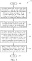
- FIG. 3 is a flow chart of a controlling method 30 according to an embodiment of the present application.
- the controlling method 30 includes the following steps:
- Step 302 Start.
- Step 304 The charge pump circuit 20 is transformed from a first mode (1/3VDD mode) to a ramp-up mode and the first output voltage HPVDD is adjusted to the voltage level of the input voltage VDD according to the up reference voltage VR UP and the second output voltage HPVSS is adjusted to the ground voltage level according to the down reference voltage VR DN .
- Step 306 The charge pump circuit 20 is transformed from the ramp-up mode to a second mode (VDD mode), the transistor switches of the digital control circuit 204 are turned on to enter the second mode.
- Step 308 The charge pump circuit 20 is transformed from the second mode to a balance release mode, the loading resistor RL discharges the first output voltage HPVDD and charges the second output voltage HPVSS, and the common mode voltage V cm of the first output voltage HPVDD and the second output voltage HPVSS is maintained by the common mode feedback loop of the balance release circuit 208.
- Step 310 When a voltage level of the logic signal DNOK of the balance release circuit 208 is changed, the charge pump circuit 20 is transformed from the balance release mode to the first mode.
- Step 312 End.
- the charge pump circuit 20 is configured to operate among the first mode, the ramp-up mode, the second mode and the balance release mode by the switch module 202, the digital control circuit 204 and the balance release circuit 208.
- the charge pump circuit 20 generates the first output voltage HPVDD and the second output voltage HPVSS with three different phases by switching the switches S1-S6 and the soft ramp-up switch S1 soft of the switch module 202.
- the switches S1-S6 are stopped switching to enter the ramp-up mode.
- the first output voltage HPVDD is adjusted to the voltage level of the input voltage VDD according to the up reference voltage VR UP
- the second output voltage HPVSS is adjusted to the ground voltage level GND according to the down reference voltage VR DN .
- the up reference voltage VR UP is generated by the up digital signal D UP and the down reference voltage VR DN is generated by the down digital signal D DN , the variation speeds of the first output voltage HPVDD and the second output voltage HPVSS are dynamically varied in time with the input signal of the class-G amplifier circuit 10.
- step 306 when the charge pump circuit 20 is transformed from the ramp-up mode to the second mode, the transistor switches M UP , M DN are turned on to connect to the input voltage VDD and the ground voltage level GND and enter the second mode.
- the first output voltage HPVDD and the second output voltage HPVSS are only related to the up reference voltage VR UP and the down reference voltage VR DN .
- the up reference voltage VR UP and the down reference voltage VR DN are controlled by the up digital signal D UP and the down digital signal D DN of the charge pump controller 206.
- step 306 of the mode transformation process larger inrush currents caused by a huge voltage difference of loading resistor RL or bias of the output capacitors C UP , C DN would not be generated by the charge pump circuit 20.
- the digital control circuit 204 since the digital control circuit 204 is connected to the first output voltage HPVDD and the second output voltage HPVSS, the digital control circuit 204 may precisely predict the first output voltage HPVDD and the second output voltage HPVSS of the switch module 202. Therefore, based on the variation speed of the input signal (i.e.
- the up digital signal D UP and the down digital signal D DN ) of the charge pump circuit 20 are adaptively changed in time, so as to reduce the inrush currents without clipping of the output of the class-G amplifier circuit 10.
- step 308 the charge pump circuit 20 is transformed from the second mode to the balance release mode, the switching operation of the switches S1-S6 is stopped, and the switch S BR is turned on, such that the loading resistor RL and the capacitors C UP , C DN discharge the first output voltage HPVDD, and charge the second output voltage HPVSS. Then, the common mode voltage of the first output voltage HPVDD and the second output voltage HPVSS is maintained at V cm (i.e. VDD/2)by the common mode feedback loop of the balance release circuit 208.
- V cm i.e. VDD/2
- step 310 when the first output voltage HPVDD is determined smaller than 2 ⁇ VDD/3 or when the second output voltage HPVSS is determined larger than VDD/3 by the logic circuit LC, the voltage level of the logic signal DNOK is changed.
- the charge pump circuit 20 is transformed from the balance release mode to the first mode according to the variation of the voltage level of the logic signal DNOK, e.g. from the low voltage level to the high voltage level, and the charge pump controller 206 is notified by the logic signal DNOK.
- the efficiency of the class-G amplifier circuit 10 may be improved.
- capacitance values of the capacitors C UP , C DN mismatch the variation speeds of the first output voltage HPVDD and the second output voltage HPVSS when charging/discharging are not identical, which generates larger inrush currents when the charge pump circuit 20 is transformed to the first mode with only one (i.e. the first output voltage HPVDD or the second output voltage HPVSS) achieving a stable state voltage of the first mode.
- the common mode voltage of the first output voltage HPVDD and the second output voltage HPVSS is maintained at VDD/2 by the feedback control of the common mode feedback circuit of the balance release circuit 208.
- the capacitance values of the capacitors C UP , C DN mismatch the stable state voltage of the first mode is achieved and the larger inrush currents are prevented when the charge pump circuit 20 is transformed from the balance release mode to the first mode, the first output voltage HPVDD is 2 ⁇ VDD/3 and the second output voltage HPVSS is VDD/3.
- Table 1 shows a state table of the switches (on/off) of the charge pump circuit 20 in different modes: Table 1 Phase S1 soft S1 S2 S3 S4 S5 S6 S7 S8 S9 S BR First Mode 1 off on off on off off off off on off off off off off 2 off off on off off on off on off off off off off off 3 off off off off off on off on on off off off off off off Ramp-up Mode off off on off off on off off off on off Second Mode off off on off off on off off off on off off off off off off off off off off off off Balance Release Mode off off on off off on off on off off off on off off on off off on on off off on on off off on on off on on off on on on off on on on off on on on off on on on off on on on off on on on off on on on off on on on off on on on off on on on off on on on off on on on off on on on off on on on off on on on off on on on off on on on off on on on off on on on off off on on
- the embodiments mentioned above are to briefly illustrate concepts of the present application, and those skilled in the art may make modifications thereto.
- the switches mentioned above may be implemented by transistor switches or other switches, or the logic circuit may be implemented by other circuits with the same function and not limited thereto, which all belong to the scope of the present application.
- the charge pump circuit of the present application locks the output voltage according to the input signal and adaptively changes the mode transformation speed according to the input signal so as to reduce the inrush currents, avoid circumstances of distortions generated by pop noises or clipping and optimize the efficiency of the amplifier.
Landscapes
- Engineering & Computer Science (AREA)
- Power Engineering (AREA)
- Amplifiers (AREA)
- Dc-Dc Converters (AREA)
Abstract
Description
- The present application relates to a charge pump circuit and controlling method thereof, and more particularly, to a charge pump circuit and controlling method thereof capable of reducing inrush currents generated when transforming among voltage modes.
- Compared to a conventional class-AB amplifier, a class-G amplifier may be configured to dynamically adjust a power voltage and greatly improve power efficiency and is widely utilized in audio applications. Please refer to
FIG. 1 , which is a structural diagram of a conventional class-G amplifier circuit 10 with a digital input. The conventional class-G amplifier circuit 10 includes a digitalfront end circuit 102, a digital-to-analog converter (DAC) 104, a class-AB amplifier 106, a charge-pumpcontrol logic circuit 108 and acharge pump circuit 110. The charge-pumpcontrol logic circuit 108 adjusts an output voltage of thecharge pump circuit 110 according to an input signal, such that thecharge pump circuit 110 may transform among different voltage modes. - To avoid larger inrush currents generated when transforming modes, before the conventional
charge pump circuit 110 is transformed from a 1/3VDD mode to a VDD mode, the conventionalcharge pump circuit 110 enters a soft ramp-up mode, an output voltage of thecharge pump circuit 110 is charged by a smaller fixed current. After thecharge pump circuit 110 is charged for a fixed time period, thecharge pump circuit 110 enters the VDD mode. When thecharge pump circuit 110 is transformed from the VDD mode to the 1/3VDD mode, a three-phase soft switching is utilized for transforming the output voltage to the 1/3VDD mode. However, a charging time period of the conventionalcharge pump circuit 110 is fixed during the soft ramp-up mode. If the charging period is not long enough, thecharge pump circuit 110 enters the VDD mode and huge inrush currents are generated, which causes distortions when the class-G amplifier circuit is applied on the audio and generates pop noises. In contrast, if the charging period is too long, a ramp-up process of the output voltage is too slow and causes clipping of the output voltage of the class-G amplifier circuit and distortions. In addition, the charging time of the output voltage of the charge pump circuit 100 is easily affected by an output device and loading current, which makes digital control logic of the class-G amplifier circuit difficult. Moreover, a time period needed for the transformation to the 1/3VDD is directly related to the loading current and output capacitors. When the time period is too short, the output voltage of the charge pump circuit 100 cannot be reduced to the 1/3VDD mode. In contrast, if the time period is too long, the output voltage is lower than 1/3VDD due to a huge impedance caused by the soft switching of the charge pump circuit 100, which generates huge inrush currents. - Therefore, how to provide a charge pump circuit capable of minimizing the inrush currents during the mode transformations, so as to avoid circumstances of distortions caused by the pop noises or clipping and optimize the efficiency of the amplifier, has been an object in the industry.
- It is therefore an object of the present application to provide a charge pump circuit and controlling method to avoid circumstances of distortion caused by the generated pop noises or clipping and optimize the efficiency of the class-G amplifier circuit.
- To solve the technical problems mentioned above, the present application provides a digital control circuit, configured to receive a up digital signal and a down digital signal, and adjust a first output voltage to a voltage level of an input voltage and adjust an second output voltage to a ground voltage level according to the up digital signal and the down digital signal, comprises a digital-to-analog converter (DAC), configured to generate a corresponding up reference voltage and a corresponding down reference voltage according to the up digital signal and the down digital signal; and a voltage follower, comprising a plurality of operational amplifiers and a plurality of transistor switches, configured to lock the first output voltage and the second output voltage according to the up reference voltage and the down reference voltage; wherein the up digital signal and the down digital signal are varied with time.
- An embodiment of the present application provides a charge pump circuit, comprises a digital control circuit, coupled to a switch module of the charge pump, configured to receive a up digital signal and a down digital signal, and adjust a first output voltage to a voltage level of an input voltage and adjust an second output voltage to a ground voltage level according to the up digital signal and the down digital signal, comprises a digital-to-analog converter (DAC), configured to generate a corresponding up reference voltage and a corresponding down reference voltage according to the up digital signal and the down digital signal; and a voltage follower, comprising a plurality of operational amplifiers and a plurality of transistor switches, configured to lock the first output voltage and the second output voltage according to the up reference voltage and the down reference voltage.
- Preferably, the charge pump circuit further comprises a balance release circuit, coupled to the digital control circuit and the switch module, configured to maintain a common mode voltage of the first output voltage and the second output voltage at a fixed value through a common mode feedback loop, when the first output voltage and the second output voltage is discharging or charging; wherein the common mode voltage is half of the input voltage; wherein the common mode feedback loop includes a plurality of operational amplifiers and a plurality of resistors.
- Preferably, the switch module, comprises a plurality of switches, a plurality of output capacitors, a loading resistor and a soft ramp-up switch, and is configured to generate the first output voltage and the second output voltage according to the input voltage and control the plurality of switches and the soft ramp-up switch to transform the first output voltage and the second output voltage with a first mode, a ramp-up mode, a second mode and a balance release mode.
- Preferably, when the charge pump circuit is transformed from the first mode to the ramp-up mode, the first output voltage is adjusted to the voltage level of the input voltage according to the up reference voltage and the second output voltage is adjusted to the ground voltage level according to the down reference voltage.
- Preferably, when the charge pump circuit is transformed from the ramp-up mode to the second mode, the plurality of transistor switches of the digital control circuit are turned on to connect the input voltage and the ground voltage level to enter the second mode.
- Preferably, the first output voltage and the second output voltage are only related to the up reference voltage and the down reference voltage.
- Preferably, the digital control circuit is connected to the first output voltage and the second output voltage.
- Preferably, when the charge pump circuit is transformed from the second mode to the balance release mode, the first output voltage is discharged and the second output voltage is charged by the loading resistor and the plurality of capacitors, the common mode voltage of the first output voltage and the second output voltage is maintained at the fixed value by the common mode feedback loop of the balance release circuit.
- Preferably, when the charge pump circuit is transformed from the second mode to the balance release mode, a switching operation of the plurality of switches of the switch module is stopped, and a switch of the common mode feedback loop is turned on.
- Preferably, the fixed value is half of the input voltage.
- Preferably, when the first output voltage and the second output voltage are completely discharged, the charge pump circuit is transformed from the balance release mode to the first mode.
- Preferably, wherein when the first output voltage is determined smaller than 2/3 of the input voltage or when the second output voltage is determined larger than 1/3 of the input voltage by a logic circuit, a voltage level of a logic signal is changed; the charge pump circuit is transformed from the balance release mode to the first mode according to a variation of the voltage level of the logic signal; and a charge pump controller is notified by the logic signal.
- Preferably, when the charge pump circuit is transformed from the balance release mode to the first mode, the first output voltage is 2/3 of the input voltage and the second output voltage HPVSS is 1/3 of the input voltage, so as to achieve a stable state voltage of the first mode.
- An embodiment of the present application provides a controlling method for a charge pump circuit, comprises receiving a up digital signal and a down digital signal; converting the up digital signal and the down digital signal to a up reference voltage and a down reference voltage; adjusting a first output voltage to a voltage level of an input voltage and an second output voltage to a ground voltage level according to the up reference voltage and the down reference voltage; turning on a plurality of transistor switches of the digital control circuit of the charge pump circuit to connect the input voltage and a ground voltage level; discharging the first output voltage and charging the second output voltage; and maintaining a common mode voltage of the first output voltage and the second output voltage at a fixed value by a common mode feedback loop.
- The charge pump circuit of the present application locks the output voltage of the charge pump circuit according to the input signal to reduce inrush currents during the mode transformation, so as to avoid circumstances of distortions caused by pop noises or clipping generated by the class-G amplifier circuit. In addition, since the energy discharged by the charge pump circuit is completely consumed on the loading resistor in the balance release mode, which is more capable of optimizing the efficiency of the class-G amplifier circuit compared with the soft switching mode of the conventional charge pump circuit.
-
-
FIG. 1 is a schematic diagram of a conventional class-G amplifier. -
FIG. 2 is a schematic diagram of a charge pump circuit according to an embodiment of the present application. -
FIG. 3 is a flow chart of a controlling method according to an embodiment of the present application. -
FIG. 4 is a schematic diagram of a mode transformation of a charge pump circuit according to an embodiment of the present application. - In order to make the objects, technical solutions and advantages of the present application become more apparent, the following relies on the accompanying drawings and embodiments to describe the present application in further detail. It should be understood that the specific embodiments described herein are only for explaining the present application and are not intended to limit the present application.
- Please refer to
FIG.2 , which is a schematic diagram of acharge pump circuit 20 according to an embodiment of the present application. Thecharge pump circuit 20 includes aswitch module 202, adigital control circuit 204 and abalance release circuit 208. Theswitch module 202 is configured to generate a first output voltage HPVDD and a second output voltage HPVSS according to an input voltage VDD, which includes switches S1, S2, S3, S4, S5, S6, output capacitors CUP, CDN, a loading resistor RL and a soft ramp-up switch S1soft. Thedigital control circuit 204 is configured to lock the first output voltage HPVDD and the second output voltage HPVSS. Thebalance release circuit 208 is configured to maintain a common mode voltage of the first output voltage and the second output voltage at Vcm through a common mode feedback loop, when the first output voltage HPVDD and the second output voltage HPVSS is discharging or charging. Acharge pump controller 206 is configured to output an up digital signal DUP and a down digital signal DDN, and adjust the first output voltage HPVDD to a voltage level of the input voltage VDD, and adjust the second output voltage HPVSS to a voltage level of GND. In addition, thecharge pump controller 206 is configured to determine whether a mode transformation process of thecharge pump circuit 20 is completed or not according to a logic signal DNOK. Therefore, thecharge pump circuit 20 of the present application locks the first output voltage HPVDD and the second output voltage HPVSS of theswitch module 202 by thedigital control circuit 204 and thebalance release circuit 208, so as to reduce inrush currents generated during the mode transformation of thecharge pump circuit 20 and consume all discharged energy on the loading resistor to increase the power efficiency of thecharge pump circuit 20. - In detail, the
digital control circuit 204 includes a digital-to-analog converter DAC and a voltage follower Vf, wherein the digital-to-analog converter DAC is configured to generate a corresponding up reference voltage VRUP and a corresponding down reference voltage VRDN according to the up digital signal DUP and the down digital signal DDN. The voltage follower Vf includes switches S7, S8, S9, an operational amplifier Op and transistor switches MUP, MDN to lock the first output voltage HPVDD and the second output voltage HPVSS respectively according to the up reference voltage VRUP and the down reference voltage VRDN. Notably, since the up reference voltage VRUP is generated by the up digital signal DUP, and the down reference voltage VRDN is generated by the down digital signal DDN, variation speeds of the first output voltage HPVDD and the second output voltage HPVSS are dynamically varied in time according to the input signal of the class-G amplifier circuit 10. That is, the first output voltage HPVDD is only related to the up reference voltage VRUP in an ascending process, and the second output voltage HPVSS is only related to the down reference voltage VRDN in a descending process, so as to avoid clipping of the class-G amplifier circuit 10 because the first output voltage HPVDD and the second output voltage HPVSS are incapable of varying in time. Thebalance release circuit 208 includes a logic circuit LC and the common mode feedback loop, wherein the common mode feedback loop includes a common mode operational amplifier OPcm, a switch SBR and a common mode resistor Rcm, so as to detect a common mode voltage Vcm when the first output voltage HPVDD and the second output voltage HPVSS are freely discharged or charged and maintain an average value of the first output voltage HPVDD and the second output voltage HPVSS at VDD/2 by a feedback control. When the first output voltage HPVDD is smaller than 2∗VDD/3 or when the second output voltage HPVSS is larger than VDD/3, which represents that the first output voltage HPVDD and the second output voltage HPVSS are completely discharged or charged, the logic signal DNOK of thebalance release circuit 208 is changed from a low voltage level (DNOK=LOW) to a high voltage level (DNOK=HIGH) and thecharge pump controller 206 is notified. - Regarding an operation method of the
charge pump circuit 20, please refer toFIG. 3 , which is a flow chart of a controllingmethod 30 according to an embodiment of the present application. The controllingmethod 30 includes the following steps: - Step 304: The
charge pump circuit 20 is transformed from a first mode (1/3VDD mode) to a ramp-up mode and the first output voltage HPVDD is adjusted to the voltage level of the input voltage VDD according to the up reference voltage VRUP and the second output voltage HPVSS is adjusted to the ground voltage level according to the down reference voltage VRDN. - Step 306: The
charge pump circuit 20 is transformed from the ramp-up mode to a second mode (VDD mode), the transistor switches of thedigital control circuit 204 are turned on to enter the second mode. - Step 308: The
charge pump circuit 20 is transformed from the second mode to a balance release mode, the loading resistor RL discharges the first output voltage HPVDD and charges the second output voltage HPVSS, and the common mode voltage Vcm of the first output voltage HPVDD and the second output voltage HPVSS is maintained by the common mode feedback loop of thebalance release circuit 208. - Step 310: When a voltage level of the logic signal DNOK of the
balance release circuit 208 is changed, thecharge pump circuit 20 is transformed from the balance release mode to the first mode. - As can be known from the
above controlling method 30, thecharge pump circuit 20 is configured to operate among the first mode, the ramp-up mode, the second mode and the balance release mode by theswitch module 202, thedigital control circuit 204 and thebalance release circuit 208. Please refer toFIG. 4 , which is a schematic diagram of amode transformation 40 of thecharge pump circuit 20 according to an embodiment of the present application. As shown inFIG. 4 , thecharge pump circuit 20 is transformed from the first mode to the ramp-up mode, from the ramp-up mode to the second mode and from the second mode to the balance release mode by the digital control, and transformed from the balance release mode to the first mode according to the logic signal DNOK (DNOK=HIGH). - In detail, the
charge pump circuit 20 generates the first output voltage HPVDD and the second output voltage HPVSS with three different phases by switching the switches S1-S6 and the soft ramp-up switch S1soft of theswitch module 202. When thecharge pump circuit 20 is going to perform the mode transformation, instep 304, the switches S1-S6 are stopped switching to enter the ramp-up mode. In the meantime, the first output voltage HPVDD is adjusted to the voltage level of the input voltage VDD according to the up reference voltage VRUP, and the second output voltage HPVSS is adjusted to the ground voltage level GND according to the down reference voltage VRDN. Notably, since the up reference voltage VRUP is generated by the up digital signal DUP and the down reference voltage VRDN is generated by the down digital signal DDN, the variation speeds of the first output voltage HPVDD and the second output voltage HPVSS are dynamically varied in time with the input signal of the class-G amplifier circuit 10. - In
step 306, when thecharge pump circuit 20 is transformed from the ramp-up mode to the second mode, the transistor switches MUP, MDN are turned on to connect to the input voltage VDD and the ground voltage level GND and enter the second mode. In this step, the first output voltage HPVDD and the second output voltage HPVSS are only related to the up reference voltage VRUP and the down reference voltage VRDN. The up reference voltage VRUP and the down reference voltage VRDN are controlled by the up digital signal DUP and the down digital signal DDN of thecharge pump controller 206. Therefore, instep 306 of the mode transformation process, larger inrush currents caused by a huge voltage difference of loading resistor RL or bias of the output capacitors CUP, CDN would not be generated by thecharge pump circuit 20. In addition, since thedigital control circuit 204 is connected to the first output voltage HPVDD and the second output voltage HPVSS, thedigital control circuit 204 may precisely predict the first output voltage HPVDD and the second output voltage HPVSS of theswitch module 202. Therefore, based on the variation speed of the input signal (i.e. the up digital signal DUP and the down digital signal DDN) of thecharge pump circuit 20, the first output voltage HPVDD and the second output voltage HPVSS are adaptively changed in time, so as to reduce the inrush currents without clipping of the output of the class-G amplifier circuit 10. - Then, in
step 308, thecharge pump circuit 20 is transformed from the second mode to the balance release mode, the switching operation of the switches S1-S6 is stopped, and the switch SBR is turned on, such that the loading resistor RL and the capacitors CUP, CDN discharge the first output voltage HPVDD, and charge the second output voltage HPVSS. Then, the common mode voltage of the first output voltage HPVDD and the second output voltage HPVSS is maintained at Vcm (i.e. VDD/2)by the common mode feedback loop of thebalance release circuit 208. - Finally, in
step 310, when the first output voltage HPVDD is determined smaller than 2∗VDD/3 or when the second output voltage HPVSS is determined larger than VDD/3 by the logic circuit LC, the voltage level of the logic signal DNOK is changed. Thecharge pump circuit 20 is transformed from the balance release mode to the first mode according to the variation of the voltage level of the logic signal DNOK, e.g. from the low voltage level to the high voltage level, and thecharge pump controller 206 is notified by the logic signal DNOK. - Since the energy stored in the capacitors CUP, CDN may be completely released on the loading resistor RL in
step 308, the efficiency of the class-G amplifier circuit 10 may be improved. In addition, when capacitance values of the capacitors CUP, CDN mismatch, the variation speeds of the first output voltage HPVDD and the second output voltage HPVSS when charging/discharging are not identical, which generates larger inrush currents when thecharge pump circuit 20 is transformed to the first mode with only one (i.e. the first output voltage HPVDD or the second output voltage HPVSS) achieving a stable state voltage of the first mode. Therefore, in this embodiment, the common mode voltage of the first output voltage HPVDD and the second output voltage HPVSS is maintained at VDD/2 by the feedback control of the common mode feedback circuit of thebalance release circuit 208. In this way, even if the capacitance values of the capacitors CUP, CDN mismatch, the stable state voltage of the first mode is achieved and the larger inrush currents are prevented when thecharge pump circuit 20 is transformed from the balance release mode to the first mode, the first output voltage HPVDD is 2∗VDD/3 and the second output voltage HPVSS is VDD/3. - Table 1 shows a state table of the switches (on/off) of the
charge pump circuit 20 in different modes:Table 1 Phase S1 soft S1 S2 S3 S4 S5 S6 S7 S8 S9 SBR First Mode 1 off on off on off off off on off off off 2 off off on off off on off on off off off 3 off off off off on off on on off off off Ramp-up Mode off off on off off on off off off on off Second Mode off off on off off on off off on off off Balance Release Mode off off on off off on off on off off on - Notably, the embodiments mentioned above are to briefly illustrate concepts of the present application, and those skilled in the art may make modifications thereto. For example, the switches mentioned above may be implemented by transistor switches or other switches, or the logic circuit may be implemented by other circuits with the same function and not limited thereto, which all belong to the scope of the present application.
- In summary, during the mode transformation, the charge pump circuit of the present application locks the output voltage according to the input signal and adaptively changes the mode transformation speed according to the input signal so as to reduce the inrush currents, avoid circumstances of distortions generated by pop noises or clipping and optimize the efficiency of the amplifier.
Claims (15)
- A digital control circuit (204), configured to receive a up digital signal (DUP) and a down digital signal (DDN), and adjust a first output voltage (HPVDD) to a voltage level of an input voltage (VDD) and adjust an second output voltage (HPVSS) to a ground voltage level according to the up digital signal (DUP) and the down digital signal (DDN), comprising:a digital-to-analog converter (DAC), configured to generate a corresponding up reference voltage (VRUP) and a corresponding down reference voltage (VRDN) according to the up digital signal and the down digital signal (DDN); anda voltage follower (Vf), comprising a plurality of operational amplifiers and a plurality of transistor switches (MUP, MDN), configured to lock the first output voltage (HPVDD) and the second output voltage (HPVSS) according to the up reference voltage (VRUP) and the down reference voltage (VRDN);wherein the up digital signal (DUP) and the down digital signal (DDN) are varied with time.
- A charge pump circuit (20), comprising:
a digital control circuit (204), coupled to a switch module (202) of the charge pump, configured to receive a up digital signal (DUP) and a down digital signal (DDN), and adjust a first output voltage (HPVDD) to a voltage level of an input voltage (VDD) and adjust an second output voltage (HPVSS) to a ground voltage level according to the up digital signal (DUP) and the down digital signal (DDN), comprising:a digital-to-analog converter (DAC), configured to generate a corresponding up reference voltage (VRUP) and a corresponding down reference voltage (VRDN) according to the up digital signal (DUP) and the down digital signal (DDN); anda voltage follower (Vf), comprising a plurality of operational amplifiers (OP) and a plurality of transistor switches (MUP, MDN), configured to lock the first output voltage (HPVDD) and the second output voltage (HPVSS) according to the up reference voltage (VRUP) and the down reference voltage (VRDN). - The charge pump circuit (20) of claim 2, further comprising:a balance release circuit, coupled to the digital control circuit (204) and the switch module (202), configured to maintain a common mode voltage (Vcm) of the first output voltage (HPVDD) and the second output voltage (HPVSS) at a fixed value through a common mode feedback loop (OPcm), when the first output voltage (HPVDD) and the second output voltage (HPVSS) is discharging or charging;wherein the common mode voltage (Vcm) is half of the input voltage (VDD);wherein the common mode feedback loop (OPcm) includes a plurality of operational amplifiers (OP) and a plurality of resistors (Rcm).
- The charge pump circuit (20) of claim 3, wherein the switch module (202), comprises a plurality of switches (S 1-S6), a plurality of output capacitors (CUP, CDN), a loading resistor (RL) and a soft ramp-up switch (S1soft), and is configured to generate the first output voltage (HPVDD) and the second output voltage (HPVSS) according to the input voltage (VDD) and control the plurality of switches (S 1-S6) and the soft ramp-up switch (S1soft) to transform the first output voltage (HPVDD) and the second output voltage (HPVSS) with a first mode, a ramp-up mode, a second mode and a balance release mode.
- The charge pump circuit (20) of claim 4, wherein when the charge pump circuit (20) is transformed from the first mode to the ramp-up mode, the first output voltage (HPVDD) is adjusted to the voltage level of the input voltage (VDD) according to the up reference voltage (VRUP) and the second output voltage (HPVSS) is adjusted to the ground voltage level according to the down reference voltage (VRDN).
- The charge pump circuit (20) of claim 4, wherein when the charge pump circuit (20) is transformed from the ramp-up mode to the second mode, the plurality of transistor switches (MUP, MDN) of the digital control circuit (204) are turned on to connect the input voltage (VDD) and the ground voltage level to enter the second mode.
- The charge pump circuit (20) of claim 6, wherein the first output voltage (HPVDD) and the second output voltage (HPVSS) are only related to the up reference voltage (VRUP) and the down reference voltage (VRDN).
- The charge pump circuit (20) of claim 6, wherein the digital control circuit (204) is connected to the first output voltage (HPVDD) and the second output voltage.
- The charge pump circuit (20) of claim 4, wherein when the charge pump circuit (20) is transformed from the second mode to the balance release mode, the first output voltage (HPVDD) is discharged and the second output voltage (HPVSS) is charged by the loading resistor (RL) and the plurality of capacitors, the common mode voltage (Vcm) of the first output voltage (HPVDD) and the second output voltage (HPVSS) is maintained at the fixed value by the common mode feedback loop (OPcm) of the balance release circuit.
- The charge pump circuit (20) of claim 9, wherein when the charge pump circuit (20) is transformed from the second mode to the balance release mode, a switching operation of the plurality of switches (S1-S6) of the switch module (202) is stopped, and a switch of the common mode feedback loop (OPcm) is turned on.
- The charge pump circuit (20) of claim 10, wherein the fixed value is half of the input voltage (VDD).
- The charge pump circuit (20) of claim 4, wherein when the first output voltage (HPVDD) and the second output voltage (HPVSS) are completely discharged, the charge pump circuit (20) is transformed from the balance release mode to the first mode.
- The charge pump circuit (20) of claim 12, wherein when the first output voltage (HPVDD) is determined smaller than 2/3 of the input voltage (VDD) or when the second output voltage (HPVSS) is determined larger than 1/3 of the input voltage (VDD) by a logic circuit, a voltage level of a logic signal is changed; the charge pump circuit (20) is transformed from the balance release mode to the first mode according to a variation of the voltage level of the logic signal; and a charge pump controller is notified by the logic signal.
- The charge pump circuit (20) of claim 12, wherein when the charge pump circuit (20) is transformed from the balance release mode to the first mode, the first output voltage (HPVDD) is 2/3 of the input voltage (VDD) and the second output voltage (HPVSS) is 1/3 of the input voltage (VDD), so as to achieve a stable state voltage of the first mode.
- A controlling method (30) for a charge pump circuit (20), comprising:receiving a up digital signal (DUP) and a down digital signal (DDN);converting the up digital signal (DUP) and the down digital signal (DDN) to a up reference voltage (VRUP) and a down reference voltage (VRDN);adjusting a first output voltage (HPVDD) to a voltage level of an input voltage (VDD) and an second output voltage (HPVSS) to a ground voltage level according to the up reference voltage (VRUP) and the down reference voltage (VRDN);turning on a plurality of transistor switches (MUP, MDN) of the digital control circuit (204) of the charge pump circuit (20) to connect the input voltage (VDD) and a ground voltage level;discharging the first output voltage (HPVDD) and charging the second output voltage; andmaintaining a common mode voltage (Vcm) of the first output voltage (HPVDD) and the second output voltage (HPVSS) at a fixed value by a common mode feedback loop (OPcm).
Priority Applications (1)
| Application Number | Priority Date | Filing Date | Title |
|---|---|---|---|
| EP21173565.9A EP3883110B1 (en) | 2018-04-12 | 2018-04-12 | Digital control circuit, charge pump circuit and controlling method thereof |
Applications Claiming Priority (3)
| Application Number | Priority Date | Filing Date | Title |
|---|---|---|---|
| PCT/CN2018/082867 WO2019196064A1 (en) | 2018-04-12 | 2018-04-12 | Charge pump circuit and control method therefor |
| EP21173565.9A EP3883110B1 (en) | 2018-04-12 | 2018-04-12 | Digital control circuit, charge pump circuit and controlling method thereof |
| EP18897875.3A EP3579393B1 (en) | 2018-04-12 | 2018-04-12 | Charge pump circuit and control method therefor |
Related Parent Applications (2)
| Application Number | Title | Priority Date | Filing Date |
|---|---|---|---|
| EP18897875.3A Division EP3579393B1 (en) | 2018-04-12 | 2018-04-12 | Charge pump circuit and control method therefor |
| EP18897875.3A Division-Into EP3579393B1 (en) | 2018-04-12 | 2018-04-12 | Charge pump circuit and control method therefor |
Publications (2)
| Publication Number | Publication Date |
|---|---|
| EP3883110A1 true EP3883110A1 (en) | 2021-09-22 |
| EP3883110B1 EP3883110B1 (en) | 2024-12-04 |
Family
ID=68162285
Family Applications (2)
| Application Number | Title | Priority Date | Filing Date |
|---|---|---|---|
| EP21173565.9A Active EP3883110B1 (en) | 2018-04-12 | 2018-04-12 | Digital control circuit, charge pump circuit and controlling method thereof |
| EP18897875.3A Active EP3579393B1 (en) | 2018-04-12 | 2018-04-12 | Charge pump circuit and control method therefor |
Family Applications After (1)
| Application Number | Title | Priority Date | Filing Date |
|---|---|---|---|
| EP18897875.3A Active EP3579393B1 (en) | 2018-04-12 | 2018-04-12 | Charge pump circuit and control method therefor |
Country Status (4)
| Country | Link |
|---|---|
| US (2) | US10615688B2 (en) |
| EP (2) | EP3883110B1 (en) |
| CN (1) | CN110612659B (en) |
| WO (1) | WO2019196064A1 (en) |
Families Citing this family (3)
| Publication number | Priority date | Publication date | Assignee | Title |
|---|---|---|---|---|
| CN110557012B (en) * | 2019-09-11 | 2020-07-17 | 上海南芯半导体科技有限公司 | For the following 2: 1 forward charge pump driving circuit and implementation method thereof |
| CN115509293B (en) * | 2022-09-15 | 2024-01-23 | 中国船舶重工集团公司七五0试验场 | Sonar emission power regulation circuit, system and control method |
| TWI878942B (en) * | 2023-06-30 | 2025-04-01 | 瑞昱半導體股份有限公司 | Switched capacitor circuit and pipelined analog-to-digital convertor including the same |
Citations (2)
| Publication number | Priority date | Publication date | Assignee | Title |
|---|---|---|---|---|
| US20080116979A1 (en) * | 2006-06-30 | 2008-05-22 | Lesso John P | Amplifier circuit and methods of operation thereof |
| US9651961B2 (en) * | 2011-12-27 | 2017-05-16 | Intel Corporation | Multi-mode voltage regulation with feedback |
Family Cites Families (16)
| Publication number | Priority date | Publication date | Assignee | Title |
|---|---|---|---|---|
| US5841248A (en) * | 1997-04-30 | 1998-11-24 | Rca Thomson Licensing Corporation | Charge controlled raster correction circuit |
| TWI307213B (en) * | 2005-08-02 | 2009-03-01 | Realtek Semiconductor Corp | Reference voltage generating circuit |
| TWI311403B (en) * | 2005-08-30 | 2009-06-21 | Realtek Semiconductor Corp | Reference voltage generating circuit |
| TWI327008B (en) * | 2006-07-28 | 2010-07-01 | Mstar Semiconductor Inc | Delta-sigma modulated fractional-n pll frequency synthesizer |
| US7518455B2 (en) * | 2006-07-28 | 2009-04-14 | Mstar Semiconductor, Inc. | Delta-sigma modulated fractional-N PLL frequency synthesizer |
| CN101334680B (en) * | 2007-06-29 | 2011-04-20 | 群康科技(深圳)有限公司 | Public voltage generation circuit and LCD device |
| US8044706B2 (en) * | 2009-10-09 | 2011-10-25 | Dialog Semiconductor Gmbh | Reduced capacitor charge-pump |
| CN102347687B (en) * | 2010-08-04 | 2014-09-24 | 宏碁股份有限公司 | charge pump |
| TW201244328A (en) * | 2011-04-28 | 2012-11-01 | Hycon Technology Corp | Micro control unit for providing stable voltage output to electric device and system for protecting electric device |
| US8970298B2 (en) * | 2011-09-02 | 2015-03-03 | Tempo Semiconductor, Inc. | Digitally controlled power supplies for an audio amplifier |
| TWM462685U (en) * | 2012-12-06 | 2013-10-01 | Vehicle Semiconductor Technology Company Ltd E | Charge pump circuit with leakage breaker |
| CN203912260U (en) * | 2014-05-06 | 2014-10-29 | 深圳市绿源半导体技术有限公司 | Charge control device for LED driving circuit, and LED driving circuit |
| CN105321544A (en) * | 2015-11-27 | 2016-02-10 | 成都思博特科技有限公司 | Analog-digital conversion type novel recording system based on pre-amplification circuit |
| US9705512B1 (en) * | 2016-09-20 | 2017-07-11 | Realtek Semiconductor Corporation | Self-calibrating fractional-N phase lock loop and method thereof |
| US9960737B1 (en) * | 2017-03-06 | 2018-05-01 | Psemi Corporation | Stacked PA power control |
| US10199928B1 (en) * | 2018-01-19 | 2019-02-05 | Infineon Technologies Austria Ag | Soft start of switched capacitor converters by reducing voltage provided by initial power switch |
-
2018
- 2018-04-12 EP EP21173565.9A patent/EP3883110B1/en active Active
- 2018-04-12 WO PCT/CN2018/082867 patent/WO2019196064A1/en not_active Ceased
- 2018-04-12 CN CN201880000385.8A patent/CN110612659B/en active Active
- 2018-04-12 EP EP18897875.3A patent/EP3579393B1/en active Active
-
2019
- 2019-06-25 US US16/452,456 patent/US10615688B2/en active Active
-
2020
- 2020-02-23 US US16/798,413 patent/US10727739B2/en active Active
Patent Citations (2)
| Publication number | Priority date | Publication date | Assignee | Title |
|---|---|---|---|---|
| US20080116979A1 (en) * | 2006-06-30 | 2008-05-22 | Lesso John P | Amplifier circuit and methods of operation thereof |
| US9651961B2 (en) * | 2011-12-27 | 2017-05-16 | Intel Corporation | Multi-mode voltage regulation with feedback |
Non-Patent Citations (1)
| Title |
|---|
| HARSHIL JADA ET AL: "A programmable low dropout regulator for delay correction network in DPWM", 2015 4TH INTERNATIONAL CONFERENCE ON RELIABILITY, INFOCOM TECHNOLOGIES AND OPTIMIZATION (ICRITO) (TRENDS AND FUTURE DIRECTIONS), IEEE, 2 September 2015 (2015-09-02), pages 1 - 6, XP032828542, DOI: 10.1109/ICRITO.2015.7359345 * |
Also Published As
| Publication number | Publication date |
|---|---|
| EP3579393A4 (en) | 2020-02-26 |
| EP3883110B1 (en) | 2024-12-04 |
| CN110612659A (en) | 2019-12-24 |
| WO2019196064A1 (en) | 2019-10-17 |
| US20200195137A1 (en) | 2020-06-18 |
| CN110612659B (en) | 2021-10-22 |
| US20190319533A1 (en) | 2019-10-17 |
| US10615688B2 (en) | 2020-04-07 |
| US10727739B2 (en) | 2020-07-28 |
| EP3579393B1 (en) | 2021-07-07 |
| EP3579393A1 (en) | 2019-12-11 |
Similar Documents
| Publication | Publication Date | Title |
|---|---|---|
| US8310313B2 (en) | Highly efficient class-G amplifier and control method thereof | |
| US4622482A (en) | Slew rate limited driver circuit which minimizes crossover distortion | |
| US10727739B2 (en) | Charge pump circuit and controlling method thereof | |
| US10256777B2 (en) | Audio amplifiers | |
| CN110612665B (en) | Calibration of an amplifier with a configurable final output stage | |
| CN103988406A (en) | Switched average frequency control for envelope tracking | |
| US20130249626A1 (en) | Multiple power mode amplifier | |
| CN101710824B (en) | Class D amplifier | |
| WO2005006528A1 (en) | Power supply having multi-vector error amplifier for power factor correction | |
| US20100060248A1 (en) | Soft-start voltage circuit | |
| WO2007035724A2 (en) | Soft-start circuit and method for power-up of an amplifier circuit | |
| USRE41926E1 (en) | Output circuit for adjusting output voltage slew rate | |
| US11205999B2 (en) | Amplifier with signal dependent mode operation | |
| US7855668B2 (en) | Delta sigma A/D modulator | |
| US20250211185A1 (en) | Adaptive equalizer device | |
| CN107196546A (en) | A kind of active discharge system of electric machine controller | |
| WO2023226971A1 (en) | Voltage stabilizing circuit and voltage stabilizing method therefor, integrated circuit, and electronic device | |
| US20200127613A1 (en) | Audio Processing Circuit and Terminal Device | |
| CN112585867B (en) | Apparatus and method for envelope tracking with transient response in supply voltage for auxiliary power amplifier | |
| US12580539B2 (en) | Transimpedance amplifier circuit | |
| EP4057506A1 (en) | Operational amplifier, chip and electronic device | |
| US12206418B2 (en) | Delay device and delay control method | |
| CN115996027A (en) | A Calibration Circuit for Operational Amplifier Offset | |
| US9768630B2 (en) | Real time compensating power output charging circuit | |
| US20250219584A1 (en) | Signal generator |
Legal Events
| Date | Code | Title | Description |
|---|---|---|---|
| PUAI | Public reference made under article 153(3) epc to a published international application that has entered the european phase |
Free format text: ORIGINAL CODE: 0009012 |
|
| STAA | Information on the status of an ep patent application or granted ep patent |
Free format text: STATUS: THE APPLICATION HAS BEEN PUBLISHED |
|
| AC | Divisional application: reference to earlier application |
Ref document number: 3579393 Country of ref document: EP Kind code of ref document: P |
|
| AK | Designated contracting states |
Kind code of ref document: A1 Designated state(s): AL AT BE BG CH CY CZ DE DK EE ES FI FR GB GR HR HU IE IS IT LI LT LU LV MC MK MT NL NO PL PT RO RS SE SI SK SM TR |
|
| STAA | Information on the status of an ep patent application or granted ep patent |
Free format text: STATUS: REQUEST FOR EXAMINATION WAS MADE |
|
| 17P | Request for examination filed |
Effective date: 20220318 |
|
| RBV | Designated contracting states (corrected) |
Designated state(s): AL AT BE BG CH CY CZ DE DK EE ES FI FR GB GR HR HU IE IS IT LI LT LU LV MC MK MT NL NO PL PT RO RS SE SI SK SM TR |
|
| GRAP | Despatch of communication of intention to grant a patent |
Free format text: ORIGINAL CODE: EPIDOSNIGR1 |
|
| STAA | Information on the status of an ep patent application or granted ep patent |
Free format text: STATUS: GRANT OF PATENT IS INTENDED |
|
| RIC1 | Information provided on ipc code assigned before grant |
Ipc: H02M 1/36 20070101ALN20240625BHEP Ipc: H03F 1/30 20060101ALI20240625BHEP Ipc: H03F 1/02 20060101ALI20240625BHEP Ipc: H02M 3/07 20060101AFI20240625BHEP |
|
| RIC1 | Information provided on ipc code assigned before grant |
Ipc: H02M 1/36 20070101ALN20240702BHEP Ipc: H03F 1/30 20060101ALI20240702BHEP Ipc: H03F 1/02 20060101ALI20240702BHEP Ipc: H02M 3/07 20060101AFI20240702BHEP |
|
| INTG | Intention to grant announced |
Effective date: 20240731 |
|
| GRAS | Grant fee paid |
Free format text: ORIGINAL CODE: EPIDOSNIGR3 |
|
| GRAA | (expected) grant |
Free format text: ORIGINAL CODE: 0009210 |
|
| STAA | Information on the status of an ep patent application or granted ep patent |
Free format text: STATUS: THE PATENT HAS BEEN GRANTED |
|
| AC | Divisional application: reference to earlier application |
Ref document number: 3579393 Country of ref document: EP Kind code of ref document: P |
|
| AK | Designated contracting states |
Kind code of ref document: B1 Designated state(s): AL AT BE BG CH CY CZ DE DK EE ES FI FR GB GR HR HU IE IS IT LI LT LU LV MC MK MT NL NO PL PT RO RS SE SI SK SM TR |
|
| REG | Reference to a national code |
Ref country code: CH Ref legal event code: EP |
|
| REG | Reference to a national code |
Ref country code: DE Ref legal event code: R096 Ref document number: 602018077416 Country of ref document: DE |
|
| REG | Reference to a national code |
Ref country code: IE Ref legal event code: FG4D |
|
| REG | Reference to a national code |
Ref country code: LT Ref legal event code: MG9D |
|
| REG | Reference to a national code |
Ref country code: NL Ref legal event code: MP Effective date: 20241204 |
|
| PG25 | Lapsed in a contracting state [announced via postgrant information from national office to epo] |
Ref country code: HR Free format text: LAPSE BECAUSE OF FAILURE TO SUBMIT A TRANSLATION OF THE DESCRIPTION OR TO PAY THE FEE WITHIN THE PRESCRIBED TIME-LIMIT Effective date: 20241204 |
|
| PG25 | Lapsed in a contracting state [announced via postgrant information from national office to epo] |
Ref country code: FI Free format text: LAPSE BECAUSE OF FAILURE TO SUBMIT A TRANSLATION OF THE DESCRIPTION OR TO PAY THE FEE WITHIN THE PRESCRIBED TIME-LIMIT Effective date: 20241204 |
|
| PG25 | Lapsed in a contracting state [announced via postgrant information from national office to epo] |
Ref country code: BG Free format text: LAPSE BECAUSE OF FAILURE TO SUBMIT A TRANSLATION OF THE DESCRIPTION OR TO PAY THE FEE WITHIN THE PRESCRIBED TIME-LIMIT Effective date: 20241204 |
|
| PG25 | Lapsed in a contracting state [announced via postgrant information from national office to epo] |
Ref country code: ES Free format text: LAPSE BECAUSE OF FAILURE TO SUBMIT A TRANSLATION OF THE DESCRIPTION OR TO PAY THE FEE WITHIN THE PRESCRIBED TIME-LIMIT Effective date: 20241204 |
|
| PG25 | Lapsed in a contracting state [announced via postgrant information from national office to epo] |
Ref country code: NO Free format text: LAPSE BECAUSE OF FAILURE TO SUBMIT A TRANSLATION OF THE DESCRIPTION OR TO PAY THE FEE WITHIN THE PRESCRIBED TIME-LIMIT Effective date: 20250304 |
|
| PG25 | Lapsed in a contracting state [announced via postgrant information from national office to epo] |
Ref country code: LV Free format text: LAPSE BECAUSE OF FAILURE TO SUBMIT A TRANSLATION OF THE DESCRIPTION OR TO PAY THE FEE WITHIN THE PRESCRIBED TIME-LIMIT Effective date: 20241204 Ref country code: GR Free format text: LAPSE BECAUSE OF FAILURE TO SUBMIT A TRANSLATION OF THE DESCRIPTION OR TO PAY THE FEE WITHIN THE PRESCRIBED TIME-LIMIT Effective date: 20250305 |
|
| PG25 | Lapsed in a contracting state [announced via postgrant information from national office to epo] |
Ref country code: RS Free format text: LAPSE BECAUSE OF FAILURE TO SUBMIT A TRANSLATION OF THE DESCRIPTION OR TO PAY THE FEE WITHIN THE PRESCRIBED TIME-LIMIT Effective date: 20250304 |
|
| PG25 | Lapsed in a contracting state [announced via postgrant information from national office to epo] |
Ref country code: NL Free format text: LAPSE BECAUSE OF FAILURE TO SUBMIT A TRANSLATION OF THE DESCRIPTION OR TO PAY THE FEE WITHIN THE PRESCRIBED TIME-LIMIT Effective date: 20241204 |
|
| REG | Reference to a national code |
Ref country code: AT Ref legal event code: MK05 Ref document number: 1749213 Country of ref document: AT Kind code of ref document: T Effective date: 20241204 |
|
| PG25 | Lapsed in a contracting state [announced via postgrant information from national office to epo] |
Ref country code: SM Free format text: LAPSE BECAUSE OF FAILURE TO SUBMIT A TRANSLATION OF THE DESCRIPTION OR TO PAY THE FEE WITHIN THE PRESCRIBED TIME-LIMIT Effective date: 20241204 |
|
| PG25 | Lapsed in a contracting state [announced via postgrant information from national office to epo] |
Ref country code: PL Free format text: LAPSE BECAUSE OF FAILURE TO SUBMIT A TRANSLATION OF THE DESCRIPTION OR TO PAY THE FEE WITHIN THE PRESCRIBED TIME-LIMIT Effective date: 20241204 |
|
| PG25 | Lapsed in a contracting state [announced via postgrant information from national office to epo] |
Ref country code: IS Free format text: LAPSE BECAUSE OF FAILURE TO SUBMIT A TRANSLATION OF THE DESCRIPTION OR TO PAY THE FEE WITHIN THE PRESCRIBED TIME-LIMIT Effective date: 20250404 |
|
| PG25 | Lapsed in a contracting state [announced via postgrant information from national office to epo] |
Ref country code: PT Free format text: LAPSE BECAUSE OF FAILURE TO SUBMIT A TRANSLATION OF THE DESCRIPTION OR TO PAY THE FEE WITHIN THE PRESCRIBED TIME-LIMIT Effective date: 20250404 |
|
| PG25 | Lapsed in a contracting state [announced via postgrant information from national office to epo] |
Ref country code: EE Free format text: LAPSE BECAUSE OF FAILURE TO SUBMIT A TRANSLATION OF THE DESCRIPTION OR TO PAY THE FEE WITHIN THE PRESCRIBED TIME-LIMIT Effective date: 20241204 |
|
| PG25 | Lapsed in a contracting state [announced via postgrant information from national office to epo] |
Ref country code: RO Free format text: LAPSE BECAUSE OF FAILURE TO SUBMIT A TRANSLATION OF THE DESCRIPTION OR TO PAY THE FEE WITHIN THE PRESCRIBED TIME-LIMIT Effective date: 20241204 Ref country code: AT Free format text: LAPSE BECAUSE OF FAILURE TO SUBMIT A TRANSLATION OF THE DESCRIPTION OR TO PAY THE FEE WITHIN THE PRESCRIBED TIME-LIMIT Effective date: 20241204 |
|
| PG25 | Lapsed in a contracting state [announced via postgrant information from national office to epo] |
Ref country code: SK Free format text: LAPSE BECAUSE OF FAILURE TO SUBMIT A TRANSLATION OF THE DESCRIPTION OR TO PAY THE FEE WITHIN THE PRESCRIBED TIME-LIMIT Effective date: 20241204 |
|
| PG25 | Lapsed in a contracting state [announced via postgrant information from national office to epo] |
Ref country code: CZ Free format text: LAPSE BECAUSE OF FAILURE TO SUBMIT A TRANSLATION OF THE DESCRIPTION OR TO PAY THE FEE WITHIN THE PRESCRIBED TIME-LIMIT Effective date: 20241204 |
|
| PG25 | Lapsed in a contracting state [announced via postgrant information from national office to epo] |
Ref country code: IT Free format text: LAPSE BECAUSE OF FAILURE TO SUBMIT A TRANSLATION OF THE DESCRIPTION OR TO PAY THE FEE WITHIN THE PRESCRIBED TIME-LIMIT Effective date: 20241204 |
|
| REG | Reference to a national code |
Ref country code: DE Ref legal event code: R097 Ref document number: 602018077416 Country of ref document: DE |
|
| PG25 | Lapsed in a contracting state [announced via postgrant information from national office to epo] |
Ref country code: SE Free format text: LAPSE BECAUSE OF FAILURE TO SUBMIT A TRANSLATION OF THE DESCRIPTION OR TO PAY THE FEE WITHIN THE PRESCRIBED TIME-LIMIT Effective date: 20241204 |
|
| PG25 | Lapsed in a contracting state [announced via postgrant information from national office to epo] |
Ref country code: DK Free format text: LAPSE BECAUSE OF FAILURE TO SUBMIT A TRANSLATION OF THE DESCRIPTION OR TO PAY THE FEE WITHIN THE PRESCRIBED TIME-LIMIT Effective date: 20241204 |
|
| PLBE | No opposition filed within time limit |
Free format text: ORIGINAL CODE: 0009261 |
|
| STAA | Information on the status of an ep patent application or granted ep patent |
Free format text: STATUS: NO OPPOSITION FILED WITHIN TIME LIMIT |
|
| REG | Reference to a national code |
Ref country code: CH Ref legal event code: L10 Free format text: ST27 STATUS EVENT CODE: U-0-0-L10-L00 (AS PROVIDED BY THE NATIONAL OFFICE) Effective date: 20251015 |
|
| REG | Reference to a national code |
Ref country code: DE Ref legal event code: R119 Ref document number: 602018077416 Country of ref document: DE |
|
| 26N | No opposition filed |
Effective date: 20250905 |
|
| REG | Reference to a national code |
Ref country code: CH Ref legal event code: H13 Free format text: ST27 STATUS EVENT CODE: U-0-0-H10-H13 (AS PROVIDED BY THE NATIONAL OFFICE) Effective date: 20251125 |
|
| PG25 | Lapsed in a contracting state [announced via postgrant information from national office to epo] |
Ref country code: LU Free format text: LAPSE BECAUSE OF NON-PAYMENT OF DUE FEES Effective date: 20250412 |
|
| PG25 | Lapsed in a contracting state [announced via postgrant information from national office to epo] |
Ref country code: MC Free format text: LAPSE BECAUSE OF FAILURE TO SUBMIT A TRANSLATION OF THE DESCRIPTION OR TO PAY THE FEE WITHIN THE PRESCRIBED TIME-LIMIT Effective date: 20241204 |
|
| GBPC | Gb: european patent ceased through non-payment of renewal fee |
Effective date: 20250412 |
|
| REG | Reference to a national code |
Ref country code: BE Ref legal event code: MM Effective date: 20250430 |
|
| PG25 | Lapsed in a contracting state [announced via postgrant information from national office to epo] |
Ref country code: DE Free format text: LAPSE BECAUSE OF NON-PAYMENT OF DUE FEES Effective date: 20251104 |
|
| PG25 | Lapsed in a contracting state [announced via postgrant information from national office to epo] |
Ref country code: GB Free format text: LAPSE BECAUSE OF NON-PAYMENT OF DUE FEES Effective date: 20250412 |
|
| PG25 | Lapsed in a contracting state [announced via postgrant information from national office to epo] |
Ref country code: FR Free format text: LAPSE BECAUSE OF NON-PAYMENT OF DUE FEES Effective date: 20250430 |
|
| PG25 | Lapsed in a contracting state [announced via postgrant information from national office to epo] |
Ref country code: BE Free format text: LAPSE BECAUSE OF NON-PAYMENT OF DUE FEES Effective date: 20250430 |
|
| PG25 | Lapsed in a contracting state [announced via postgrant information from national office to epo] |
Ref country code: CH Free format text: LAPSE BECAUSE OF NON-PAYMENT OF DUE FEES Effective date: 20250430 |
|
| PG25 | Lapsed in a contracting state [announced via postgrant information from national office to epo] |
Ref country code: IE Free format text: LAPSE BECAUSE OF NON-PAYMENT OF DUE FEES Effective date: 20250412 |
|
| PG25 | Lapsed in a contracting state [announced via postgrant information from national office to epo] |
Ref country code: CY Free format text: LAPSE BECAUSE OF FAILURE TO SUBMIT A TRANSLATION OF THE DESCRIPTION OR TO PAY THE FEE WITHIN THE PRESCRIBED TIME-LIMIT Effective date: 20241204 |
|
| PG25 | Lapsed in a contracting state [announced via postgrant information from national office to epo] |
Ref country code: LT Free format text: LAPSE BECAUSE OF FAILURE TO SUBMIT A TRANSLATION OF THE DESCRIPTION OR TO PAY THE FEE WITHIN THE PRESCRIBED TIME-LIMIT Effective date: 20241204 |