EP3882995A1 - Magnetoresistive element comprising discontinuous interconnect segments and magnetic memory comprising a plurality of the magnetoresistive element - Google Patents
Magnetoresistive element comprising discontinuous interconnect segments and magnetic memory comprising a plurality of the magnetoresistive element Download PDFInfo
- Publication number
- EP3882995A1 EP3882995A1 EP20315039.6A EP20315039A EP3882995A1 EP 3882995 A1 EP3882995 A1 EP 3882995A1 EP 20315039 A EP20315039 A EP 20315039A EP 3882995 A1 EP3882995 A1 EP 3882995A1
- Authority
- EP
- European Patent Office
- Prior art keywords
- layer
- writing current
- interconnect
- magnetization
- gap
- Prior art date
- Legal status (The legal status is an assumption and is not a legal conclusion. Google has not performed a legal analysis and makes no representation as to the accuracy of the status listed.)
- Pending
Links
- 230000005291 magnetic effect Effects 0.000 title claims abstract description 35
- 230000005415 magnetization Effects 0.000 claims abstract description 63
- 230000005294 ferromagnetic effect Effects 0.000 claims abstract description 31
- 230000004888 barrier function Effects 0.000 claims abstract description 9
- 230000003993 interaction Effects 0.000 claims abstract description 6
- 229910045601 alloy Inorganic materials 0.000 claims description 11
- 239000000956 alloy Substances 0.000 claims description 11
- 238000000034 method Methods 0.000 claims description 9
- 239000000463 material Substances 0.000 claims description 8
- 229910052742 iron Inorganic materials 0.000 claims description 6
- 239000000696 magnetic material Substances 0.000 claims description 6
- OKTJSMMVPCPJKN-UHFFFAOYSA-N Carbon Chemical compound [C] OKTJSMMVPCPJKN-UHFFFAOYSA-N 0.000 claims description 5
- 238000000151 deposition Methods 0.000 claims description 4
- 239000003302 ferromagnetic material Substances 0.000 claims description 4
- 239000002041 carbon nanotube Substances 0.000 claims description 3
- 229910021393 carbon nanotube Inorganic materials 0.000 claims description 3
- 239000004020 conductor Substances 0.000 claims description 3
- 229910052802 copper Inorganic materials 0.000 claims description 3
- 229910052737 gold Inorganic materials 0.000 claims description 3
- 229910052697 platinum Inorganic materials 0.000 claims description 3
- 229910052721 tungsten Inorganic materials 0.000 claims description 3
- 229910005883 NiSi Inorganic materials 0.000 claims description 2
- 229910052782 aluminium Inorganic materials 0.000 claims description 2
- 229910021389 graphene Inorganic materials 0.000 claims description 2
- 229910052709 silver Inorganic materials 0.000 claims description 2
- 238000005530 etching Methods 0.000 description 8
- 229910052751 metal Inorganic materials 0.000 description 6
- 239000002184 metal Substances 0.000 description 6
- 230000008569 process Effects 0.000 description 5
- 125000006850 spacer group Chemical group 0.000 description 5
- 238000004519 manufacturing process Methods 0.000 description 4
- 229910003321 CoFe Inorganic materials 0.000 description 3
- 229910002441 CoNi Inorganic materials 0.000 description 3
- 229910019236 CoFeB Inorganic materials 0.000 description 2
- 229910018979 CoPt Inorganic materials 0.000 description 2
- 229910001030 Iron–nickel alloy Inorganic materials 0.000 description 2
- 230000005290 antiferromagnetic effect Effects 0.000 description 2
- 239000002885 antiferromagnetic material Substances 0.000 description 2
- 230000008901 benefit Effects 0.000 description 2
- 230000008878 coupling Effects 0.000 description 2
- 238000010168 coupling process Methods 0.000 description 2
- 238000005859 coupling reaction Methods 0.000 description 2
- 238000010438 heat treatment Methods 0.000 description 2
- 229910019222 CoCrPt Inorganic materials 0.000 description 1
- 229910015136 FeMn Inorganic materials 0.000 description 1
- 229910015187 FePd Inorganic materials 0.000 description 1
- 229910005335 FePt Inorganic materials 0.000 description 1
- 230000005355 Hall effect Effects 0.000 description 1
- 229910019041 PtMn Inorganic materials 0.000 description 1
- PNEYBMLMFCGWSK-UHFFFAOYSA-N aluminium oxide Inorganic materials [O-2].[O-2].[O-2].[Al+3].[Al+3] PNEYBMLMFCGWSK-UHFFFAOYSA-N 0.000 description 1
- 238000000137 annealing Methods 0.000 description 1
- 230000009286 beneficial effect Effects 0.000 description 1
- 150000001875 compounds Chemical class 0.000 description 1
- 229910052593 corundum Inorganic materials 0.000 description 1
- 230000003247 decreasing effect Effects 0.000 description 1
- 230000006866 deterioration Effects 0.000 description 1
- 229910003460 diamond Inorganic materials 0.000 description 1
- 239000010432 diamond Substances 0.000 description 1
- 230000000694 effects Effects 0.000 description 1
- 239000012777 electrically insulating material Substances 0.000 description 1
- 229910052741 iridium Inorganic materials 0.000 description 1
- 150000002739 metals Chemical class 0.000 description 1
- 229910052759 nickel Inorganic materials 0.000 description 1
- 230000003647 oxidation Effects 0.000 description 1
- 238000007254 oxidation reaction Methods 0.000 description 1
- 229910052763 palladium Inorganic materials 0.000 description 1
- 238000007517 polishing process Methods 0.000 description 1
- 229910052761 rare earth metal Inorganic materials 0.000 description 1
- 150000002910 rare earth metals Chemical class 0.000 description 1
- 230000002040 relaxant effect Effects 0.000 description 1
- 229910052707 ruthenium Inorganic materials 0.000 description 1
- 239000000126 substance Substances 0.000 description 1
- 229910052723 transition metal Inorganic materials 0.000 description 1
- 150000003624 transition metals Chemical class 0.000 description 1
- 229910001845 yogo sapphire Inorganic materials 0.000 description 1
Images


Classifications
-
- H—ELECTRICITY
- H10—SEMICONDUCTOR DEVICES; ELECTRIC SOLID-STATE DEVICES NOT OTHERWISE PROVIDED FOR
- H10N—ELECTRIC SOLID-STATE DEVICES NOT OTHERWISE PROVIDED FOR
- H10N50/00—Galvanomagnetic devices
- H10N50/01—Manufacture or treatment
-
- G—PHYSICS
- G11—INFORMATION STORAGE
- G11C—STATIC STORES
- G11C11/00—Digital stores characterised by the use of particular electric or magnetic storage elements; Storage elements therefor
- G11C11/02—Digital stores characterised by the use of particular electric or magnetic storage elements; Storage elements therefor using magnetic elements
- G11C11/16—Digital stores characterised by the use of particular electric or magnetic storage elements; Storage elements therefor using magnetic elements using elements in which the storage effect is based on magnetic spin effect
- G11C11/161—Digital stores characterised by the use of particular electric or magnetic storage elements; Storage elements therefor using magnetic elements using elements in which the storage effect is based on magnetic spin effect details concerning the memory cell structure, e.g. the layers of the ferromagnetic memory cell
-
- G—PHYSICS
- G11—INFORMATION STORAGE
- G11C—STATIC STORES
- G11C11/00—Digital stores characterised by the use of particular electric or magnetic storage elements; Storage elements therefor
- G11C11/02—Digital stores characterised by the use of particular electric or magnetic storage elements; Storage elements therefor using magnetic elements
- G11C11/16—Digital stores characterised by the use of particular electric or magnetic storage elements; Storage elements therefor using magnetic elements using elements in which the storage effect is based on magnetic spin effect
- G11C11/165—Auxiliary circuits
- G11C11/1675—Writing or programming circuits or methods
-
- H—ELECTRICITY
- H10—SEMICONDUCTOR DEVICES; ELECTRIC SOLID-STATE DEVICES NOT OTHERWISE PROVIDED FOR
- H10B—ELECTRONIC MEMORY DEVICES
- H10B61/00—Magnetic memory devices, e.g. magnetoresistive RAM [MRAM] devices
-
- H—ELECTRICITY
- H10—SEMICONDUCTOR DEVICES; ELECTRIC SOLID-STATE DEVICES NOT OTHERWISE PROVIDED FOR
- H10B—ELECTRONIC MEMORY DEVICES
- H10B61/00—Magnetic memory devices, e.g. magnetoresistive RAM [MRAM] devices
- H10B61/10—Magnetic memory devices, e.g. magnetoresistive RAM [MRAM] devices comprising components having two electrodes, e.g. diodes or MIM elements
-
- H—ELECTRICITY
- H10—SEMICONDUCTOR DEVICES; ELECTRIC SOLID-STATE DEVICES NOT OTHERWISE PROVIDED FOR
- H10N—ELECTRIC SOLID-STATE DEVICES NOT OTHERWISE PROVIDED FOR
- H10N50/00—Galvanomagnetic devices
- H10N50/10—Magnetoresistive devices
-
- H—ELECTRICITY
- H10—SEMICONDUCTOR DEVICES; ELECTRIC SOLID-STATE DEVICES NOT OTHERWISE PROVIDED FOR
- H10N—ELECTRIC SOLID-STATE DEVICES NOT OTHERWISE PROVIDED FOR
- H10N50/00—Galvanomagnetic devices
- H10N50/80—Constructional details
-
- H—ELECTRICITY
- H10—SEMICONDUCTOR DEVICES; ELECTRIC SOLID-STATE DEVICES NOT OTHERWISE PROVIDED FOR
- H10N—ELECTRIC SOLID-STATE DEVICES NOT OTHERWISE PROVIDED FOR
- H10N50/00—Galvanomagnetic devices
- H10N50/80—Constructional details
- H10N50/85—Materials of the active region
-
- H—ELECTRICITY
- H10—SEMICONDUCTOR DEVICES; ELECTRIC SOLID-STATE DEVICES NOT OTHERWISE PROVIDED FOR
- H10N—ELECTRIC SOLID-STATE DEVICES NOT OTHERWISE PROVIDED FOR
- H10N59/00—Integrated devices, or assemblies of multiple devices, comprising at least one galvanomagnetic or Hall-effect element covered by groups H10N50/00 - H10N52/00
Definitions
- the present invention relates to a magnetoresistive element and more particularly a magnetoresistive element that has increased efficiency of the writing current and that is simpler to fabricate.
- the present invention further relates to a magnetic memory comprising a plurality of the magnetoresistive element.
- Fig 1 shows a side view of a conventional magnetoresistive memory cell comprising a magnetic tunnel junction MTJ 20 including a tunnel barrier layer 22 sandwiched between a first ferromagnetic layer 21 having a first magnetization 210 and a second ferromagnetic layer 23 having a free second magnetization 230.
- the layer 24 can comprise an electrically conductive capping layer or an antiferromagnetic layer exchange coupling the first ferromagnetic layer 21 such as to pin the first magnetization 210.
- the capping layer 24 can comprise a SAF structure including a metallic non-magnetic spacer layer and a ferromagnetic layer.
- the magnetoresistive memory cell further comprises a current line 30 extending in a plane substantially parallel to the layers 21, 22, 23 of the MTJ 20 and contacting the second ferromagnetic layer 23.
- the second magnetization 230 can be switched (magnetization reversal) by passing a writing current 31 in the current line 30. Switching of the second magnetization 230 can be performed by a spin orbit torque (SOT) interaction.
- SOT spin orbit torque
- the spin current generated by spin Hall effect and/or Rashba-Edelstein effect by writing current 31 exerts a torque on the initial orientation of the second magnetization 230 so that the orientation of the second magnetization 230 can be changed, for example, from being parallel to antiparallel to the first magnetization 210
- the SOT based switching allows for using separate read- and write-paths which is beneficial for a long life of the memory cell.
- an in-plane magnetic field (not shown) has to be applied in addition to the writing current 31 in order to deterministically switch the second magnetization 230.
- Fig. 2 shows a top view of the conventional cell of Fig. 1 .
- the current line 30 is extends in the "x-y" plane around the MTJ 20.
- the writing current 31 flowing in the current line 30 does not all flows underneath the MTJ 20.
- the effective current of the writing current 31 used for switching the second magnetization 230 is increased since the writing current 31 is evenly distributed over the width of the current line 30 and only a fraction of the writing current 31 passing below the MTJ 20 is used for the switching..
- Fabricating the conventional cell where the current line 30 has a width that is similar to the lateral dimension of the MTJ 20 is difficult. One reason is that the alignment of the MTJ 20 with the current line 30 width is complicated to achieve.
- the conventional magnetoresistive memory cell shown in Figs. 1 and 2 is usually manufactured by etching the MTJ 20 until the current line 30 is reached.
- the current line 30 serves as a etch stop layer. Since the current line 30 is typically very thin, between 1 and 10 nm, the etching process needs to be very precise.
- the present disclosure concerns a magnetoresistive element, comprising: a MTJ comprising a tunnel barrier layer sandwiched between a first ferromagnetic layer having a first magnetization, a second ferromagnetic layer having a second magnetization, and a writing current layer contacting the second ferromagnetic layer and configured for passing a writing current adapted for switching the second magnetization by a SOT interaction; an interconnect layer contacting the writing current layer and configured for supplying the writing current to the writing current layer; the interconnect layer comprising a gap configured such that the interconnect layer comprises two discontinuous interconnect segments extending along a layer plane substantially parallel to the layers of the MTJ, the interconnect segments connecting the writing current layer in series.
- the present disclosure further concerns a magnetic memory comprising a plurality of the magnetoresistive element, wherein each element is connected to another element via an interconnect segment.
- the invention provides an increased efficiency of the writing current since the writing current used for switching the second magnetization by a SOT interaction flows only underneath the second ferromagnetic layer. Because there is substantially no shunting of the writing current by a portion of the writing current layer that is not underneath the MTJ, the writing current can be reduced. Moreover, the gap between the interconnect segments forces the writing current to flow completely in the writing current layer.
- the dimensional constraint along the width of the gap can be relaxed.
- the MTJ need to be precisely positioned only along a direction perpendicular to the width of the gap. Constraint along the direction perpendicular to the width of the gap can be possibly released depending on the shape of the MTJ.
- the MTJ can be etched with the writing current layer until the interconnect layer is reached.
- the interconnect layer is thus used as the stop etch layer. Since the interconnect layer can be much thicker than the thin writing current layer, the control of the etching process can be simplified and variations between different fabricated magnetoresistive elements can be reduced. The magnetoresistive element is then easier to fabricate. Moreover, oxidation or deterioration of the writing current layer during the next process steps can be avoided.
- the interconnect layer can have a lower electrical resistance than the one of the writing current layer so that less heating occurs during the write/read operations.
- the lower electrical resistance along the current path allows for reducing the total energy needed to apply a current high enough to switch the second magnetization.
- the thickness of the writing current layer can be reduced compared to the writing current layer thickness of a conventional magnetoresistive element.
- the thickness of the current layer does not need to be controlled for the etching process and can be optimized for the passing writing current.
- Fig. 3 shows a side view
- Fig. 4 shows a top view of a magnetoresistive element 10 according to an embodiment.
- the magnetoresistive element 10 comprises a MTJ 20 comprising a tunnel barrier layer 22 sandwiched between a first ferromagnetic layer 21 having a first magnetization 210, a second ferromagnetic layer 23 having a second magnetization 230.
- the first and second ferromagnetic layers 21, 23 can comprise a ferromagnetic material including a metal or alloy having a specific perpendicular magnetic anisotropy whereby the first and second magnetizations 210, 230 are oriented substantially perpendicular to the plane of the ferromagnetic layers 21, 23 (out-of-plane, also known as perpendicular magnetic anisotropy (PMA)).
- a metal or alloy can comprise FePt, FePd, CoPt, or a rare earth/transition metal alloy, in particular GdCo, TdFeCo, or Co, Fe, CoFe, Ni, CoNi, CoFeB, FeB.
- the first and second ferromagnetic layers 21, 23 can comprise a metal or alloy with the first and second magnetizations 210, 230 being oriented parallel to the plane of the ferromagnetic layers 21, 23 (in-plane).
- metal or alloy can comprise Co, Fe, CoFe, Ni, NiFe, CoNi, CoFeB, FeB.
- the thickness of the first and second ferromagnetic layers 21, 23 can be between 0.5 nm and 10 nm and preferably between 1 and 3 nm.
- the MTJ 20 can further comprise a capping layer 24.
- the capping layer 24 can comprise an antiferromagnetic layer exchange coupling the first ferromagnetic layer 21 such as to first magnetization 210 such as to pin the first magnetization 210 in a particular direction.
- the capping layer 24 can comprise a SAF structure including a metallic non-magnetic spacer layer and a ferromagnetic layer.
- the tunnel barrier layer 22 can include a material, such as MgO or Al 2 O 3 .
- the magnetoresistive element 10 further comprises a writing current layer 30 configured for passing a writing current 31 and an electrically conductive interconnect layer 50 destined to supply the writing current 31 to the writing current layer 30.
- the interconnect layer 50 can include an electrically conductive material such as Cu, W, Au, Ag, Fe, Pt, Al, Co, Ru, Mo, NiSi, carbon nano tubes (CNT), graphene or an alloy of these elements.
- the writing current layer 30 contacts the second ferromagnetic layer 23 and is configured for passing a writing current 31 adapted for switching the second magnetization 230 by a SOT interaction.
- the writing current layer 30 comprises a SOT material, where the SOT material can include an electrically conductive material, such as Pt, W, Ir, Ru, Pd, Cu, Au, Bi, Hf, Se, Sb or of an alloy of these elements, or is formed of a stack of a plurality of layers of each of these metals.
- the current layer 30 can be made from an antiferromagnetic material.
- antiferromagnetic materials include alloys with a base of Mn such as IrMn, FeMn, PtMn, or alloys of these compounds such as PtFeMn.
- the current layer 30 can be made from a ferromagnetic material, such as Fe, Co, Ni or of an alloy of these elements.
- the writing current layer 30 has a thickness that ranges between 0.5 nm and 200 nm, more particularly between 0.5 nm and 100 nm, or less than 10 nm.
- the writing layer 30 has thickness lying in the range 0.5 nm to 5 nm.
- the writing current layer 30 has lateral dimension that are substantially the same as the one of the MTJ 20.
- the lateral dimension is in a layer plane PL substantially parallel to the layers 21, 22, 23 of the MTJ 20 (along the directions "x" and "y” in Figs. 3 and 4 ).
- the MTJ 20 including the writing current layer 30 forms a pillar 40.
- the interconnect layer 50 contacts the writing current layer 30 and extends on each side of the writing current layer 30 and MTJ 20, such that the lateral dimension along the direction "y" of the interconnect layer 50 are much larger than the lateral dimension of the writing current layer 30 and the MTJ 20.
- the interconnect layer 50 comprises a gap 34 underneath the MTJ 20.
- the gap 34 is represented as a slit underneath the MTJ 20, such that the interconnect layer 50 comprises two discontinuous interconnect segments 51 connecting the writing current layer 30 in series.
- the interconnect segments 51 extend along the layer plane PL.
- the gap 34 can be configured such that each of the interconnect segments 51 are in contact with a portion at the periphery of the writing current layer 30.
- the gap 34 can be configured to have a gap width W G being a factor of about 0.9 to 0.1 of the lateral dimension D 30 of the writing current layer 30.
- the gap 34 can comprise a gap material that is preferably an electrically insulating material.
- the gap 34 has an electrical conductivity being at least ten times smaller than that of the interconnect segments 51, such that substantially no current flows in the gap 34 but rather flows only in the interconnect segments 51 and the writing current layer 30.
- the interconnect layer 50 can have any arbitrary shape as long as the above mentioned dimensional constrains are respected.
- the discontinuous interconnect segments 51 forming the interconnect layer 50 have a trapezoidal shape but could have a rectangular shape.
- the discontinuous interconnect segments 51 do not need to be aligned symmetrically with each other and a shift along the "y" axis can be tolerated as long as the interconnect segments 51 are in contact with a portion at the periphery of the writing current layer 30.
- Wide interconnect segments 51 (large size along the "y" axis) allows for decreasing the resistance of the interconnect layer 50.
- the interconnect layer 50 has an interconnect width D 50 (along the "y" axis in Fig. 4 ) that is larger than the gap width W G .
- the interconnect width D 50 can be at least 1.5 times the gap width W G or twice the gap width W G .
- the pillar 40 can have a geometrically isotropic shape, for example a shape having substantially identical dimensions in the "x" and "y" directions, such a circular shape (as shown in Fig. 4 ) or a square shape.
- the pillar 40 can have a geometrically anisotropic shape, for example a shape having a larger dimension the "x-y" plane PL (called “long axis" afterwards).
- geometrically anisotropic shapes can include an ellipsoidal, a rectangular, a trapezoidal or a diamond shape.
- Fig. 5 shows a top view of the magnetoresistive element 10, wherein the pillar 40 has an ellipsoid shape.
- the long axis 41 of the ellipsoidal MTJ 20 can be parallel to the gap width W G .
- the long axis 41 of the pillar 40 can be perpendicular to the gap width W G or can be oriented with any angle ⁇ between 0° (parallel) and 90° (perpendicular) relative to the gap width W G .
- the long axis of the MTJ 20 can be oriented with any angle ⁇ between 10° and 80° relative to the gap width W G .
- the gap width W G can be larger, relaxing the fabrication constraint along the gap width W G (along the x axis).
- the ellipsoidal pillar 40 oriented perpendicular or with an angle greater that 0° allows for breaking the symmetry.
- the orientation of the long axis as discussed in the example of Fig. 5 can be applied to any other geometrically anisotropic shapes.
- the gap material comprises a magnetic material having a bias magnetization 60 configured for breaking the symmetry, i.e., to provide a magnetic bias field 61 adapted to interact with the second magnetization 230 such as to provide deterministically switching of the second magnetization 230 when the writing current 31 is passed.
- the bias magnetization 60 should be oriented in-plane (along the "x" axis).
- the magnetic material can have a coercivity between a few hundred to few thousand Oe.
- the gap magnetic material can comprise a ferromagnet material such as: Co, Fe, CoFe, Ni, NiFe, CoNi, CoPt, CoCrPt, CoCrTa, CoSm.
- the interconnect layer 50 can comprise an electrically insulating spacer 52 between the gap 34, the interconnect segments 51 and the writing current layer 30.
- the gap magnetic material can be electrically insulating and no electrically insulating spacer between the gap 34, the interconnect segments 51 and the writing current layer 30 is needed.
- the interconnect layer 50 (the interconnect segments 51) comprises a ferromagnetic material (ferromagnet) having a bias magnetization 60 configured to provide a magnetic bias field 61 adapted to interact with the second magnetization 230 such as to provide deterministically switching of the second magnetization 230 when the writing current 31 is passed.
- the bias magnetization 60 should be oriented in-plane (along the "x" axis).
- a method for fabricating the magnetoresistive element 10 comprises successively depositing the interconnect layer 50, forming the gap 34 in the interconnect layer 50, depositing a gap layer comprising the gap material on top of the interconnect layer 50 such as to fill the gap 34, planarizing the gap layer such as to free the upper surface of the interconnect layer 50, successively depositing the writing current layer 30, second ferromagnetic layer 23, tunnel barrier layer 22, first ferromagnetic layer 21 and capping layer 24.
- the gap 34 can be formed by using lithographic and etching steps. Planarizing the gap layer can be performed by using a chemical mechanical polishing process or lithographic and etching steps.
- the fabrication process further comprises forming the pillar 40 by performing a single etch step until the interconnect layer 50, acting as a stop layer, is reached.
- the etching step can be facilitated since a multi angle etch can be done to clean any redeposited metal on the sidewall of the pillar 40.
- the etching step can start with a 35° etch then a lower angle etch.
- the pillar 40 can have sidewalls substantially vertical or tapered.
- vertical refers to a direction "z" that is perpendicular to a layer plane PL substantially parallel to the layers 21, 22, 23 of the MTJ 20.
- the MTJ 20 can be positioned relative to the interconnect layer 50 with great precision in only one direction.
- the MTJ 20 due to the large size of the interconnect width D 50 of the interconnect layer 50 (or the interconnect segments 51), the MTJ 20 needs to be precisely positioned along the "x" direction while the dimensional constraint along the "y" axis is low such that the MTJ 20 needs not be precisely positioned along the "y" axis.
- a magnetic memory 100 comprises a plurality of the magnetoresistive element 10, wherein each magnetoresistive element 10 is connected to another one via an interconnect segment 51.
- Fig. 8 shows a side view of an exemplary magnetic memory 100 wherein the magnetoresistive element 10 connected along the interconnect layer 50 are connected alternatively above the layer plane PL and below the layer plane PL, such that two adjacent magnetoresistive elements 10 are above and below the layer plane PL.
- Fig. 9 shows a top view of the magnetic memory 100 of Fig. 8 .
- This configuration allows for switching the second magnetization 230 of two adjacent magnetoresistive elements 10 in opposed orientation, such that the second magnetization 230 is parallel to the first magnetization 210 for one magnetoresistive element 10 and the second magnetization 230 is antiparallel to the first magnetization 210 for the adjacent magnetoresistive element 10, when the writing current 31 is passed in a direction in the interconnect layer 50.
- This configuration corresponds to a differential structure wherein two magnetoresistive elements 10 are written with the same current but with different magnetization configurations.
- the magnetoresistive elements 10 can be read separately and the magnetic state of the two magnetoresistive elements 10 can be compared.
- the first magnetization 210 is pinned in the same direction for the magnetoresistive elements 10.
- the first magnetization 210 can be pinned in the same direction by using a single annealing step. More particularly, the MTJs 20 can be heated at a high temperature threshold at which the first magnetization 210 can be freely oriented. A programming magnetic field (not shown) is applied such as to orient the first magnetization 210 of the MTJs 20 in accordance to the programming magnetic field. The MTJs 20 are then cooled such as to pin the first magnetization 210 in the same programmed direction.
- Fig. 10 shows a side view
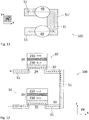
- Fig. 11 shows a top view of another arrangement of the magnetic memory 100, wherein the magnetoresistive element 10 are connected along the interconnect layer 50 having a U shape configuration.
- the magnetoresistive elements 10 are connected above of the layer plane PL (the magnetoresistive elements 10 can also be connected below of the layer plane PL).
- the interconnect layer 50 extends along a row in the layer plane PL, such that the writing current 31 flows in the writing current layer 30 of two adjacent magnetoresistive elements 10 in the row with opposed polarity.
- the interconnect segment connecting the two adjacent magnetoresistive elements 10 is indicated by the numeral 51'.
- the magnetic memory configuration of Figs. 10 and 11 also corresponds to a differential structure wherein two magnetoresistive elements 10 are written with the same current but with different magnetization configurations.
- Fig. 12 shows a side view of yet another differential arrangement of the magnetic memory 100, wherein the interconnect layer 50 has a U shape configuration extending along a column in a perpendicular plane PP substantially perpendicular to the layer plane PL.
- the writing current 31 flows in the writing current layer 30 of two adjacent magnetoresistive elements 10 in the column with opposed polarity such that the second magnetization 230 of adjacent magnetoresistive elements 10 is oriented in opposite directions.
- the magnetoresistive elements 10 are connected above of the layer plane PL, but can also be connected below the layer plane PL.
Landscapes
- Engineering & Computer Science (AREA)
- Computer Hardware Design (AREA)
- Manufacturing & Machinery (AREA)
- Hall/Mr Elements (AREA)
- Mram Or Spin Memory Techniques (AREA)
Abstract
Description
- The present invention relates to a magnetoresistive element and more particularly a magnetoresistive element that has increased efficiency of the writing current and that is simpler to fabricate. The present invention further relates to a magnetic memory comprising a plurality of the magnetoresistive element.
-
Fig 1 shows a side view of a conventional magnetoresistive memory cell comprising a magnetictunnel junction MTJ 20 including atunnel barrier layer 22 sandwiched between a firstferromagnetic layer 21 having afirst magnetization 210 and a secondferromagnetic layer 23 having a freesecond magnetization 230. Thelayer 24 can comprise an electrically conductive capping layer or an antiferromagnetic layer exchange coupling the firstferromagnetic layer 21 such as to pin thefirst magnetization 210. Alternatively, thecapping layer 24 can comprise a SAF structure including a metallic non-magnetic spacer layer and a ferromagnetic layer. The magnetoresistive memory cell further comprises acurrent line 30 extending in a plane substantially parallel to thelayers MTJ 20 and contacting the secondferromagnetic layer 23. Thesecond magnetization 230 can be switched (magnetization reversal) by passing a writing current 31 in thecurrent line 30. Switching of thesecond magnetization 230 can be performed by a spin orbit torque (SOT) interaction. The spin current generated by spin Hall effect and/or Rashba-Edelstein effect by writing current 31 exerts a torque on the initial orientation of thesecond magnetization 230 so that the orientation of thesecond magnetization 230 can be changed, for example, from being parallel to antiparallel to thefirst magnetization 210 - The SOT based switching allows for using separate read- and write-paths which is beneficial for a long life of the memory cell. In the case the
magnetizations layers 21, 23 (as shown inFig. 1 ), an in-plane magnetic field (not shown) has to be applied in addition to thewriting current 31 in order to deterministically switch thesecond magnetization 230. -
Fig. 2 shows a top view of the conventional cell ofFig. 1 . Thecurrent line 30 is extends in the "x-y" plane around the MTJ 20. As represented inFig. 2 , the writing current 31 flowing in thecurrent line 30 does not all flows underneath the MTJ 20. The effective current of thewriting current 31 used for switching thesecond magnetization 230 is increased since thewriting current 31 is evenly distributed over the width of thecurrent line 30 and only a fraction of the writing current 31 passing below theMTJ 20 is used for the switching.. Fabricating the conventional cell where thecurrent line 30 has a width that is similar to the lateral dimension of the MTJ 20 is difficult. One reason is that the alignment of theMTJ 20 with thecurrent line 30 width is complicated to achieve. - On the other hand, the conventional magnetoresistive memory cell shown in
Figs. 1 and 2 is usually manufactured by etching the MTJ 20 until thecurrent line 30 is reached. Here, thecurrent line 30 serves as a etch stop layer. Since thecurrent line 30 is typically very thin, between 1 and 10 nm, the etching process needs to be very precise. - The present disclosure concerns a magnetoresistive element, comprising: a MTJ comprising a tunnel barrier layer sandwiched between a first ferromagnetic layer having a first magnetization, a second ferromagnetic layer having a second magnetization, and a writing current layer contacting the second ferromagnetic layer and configured for passing a writing current adapted for switching the second magnetization by a SOT interaction; an interconnect layer contacting the writing current layer and configured for supplying the writing current to the writing current layer; the interconnect layer comprising a gap configured such that the interconnect layer comprises two discontinuous interconnect segments extending along a layer plane substantially parallel to the layers of the MTJ, the interconnect segments connecting the writing current layer in series.
- The present disclosure further concerns a magnetic memory comprising a plurality of the magnetoresistive element, wherein each element is connected to another element via an interconnect segment.
- With respect to what is known in the art, the invention provides an increased efficiency of the writing current since the writing current used for switching the second magnetization by a SOT interaction flows only underneath the second ferromagnetic layer. Because there is substantially no shunting of the writing current by a portion of the writing current layer that is not underneath the MTJ, the writing current can be reduced. Moreover, the gap between the interconnect segments forces the writing current to flow completely in the writing current layer.
- Thanks to the large size of the interconnect layer with respect to the size of the MTJ, the dimensional constraint along the width of the gap can be relaxed. The MTJ need to be precisely positioned only along a direction perpendicular to the width of the gap. Constraint along the direction perpendicular to the width of the gap can be possibly released depending on the shape of the MTJ.
- During the manufacturing process, the MTJ can be etched with the writing current layer until the interconnect layer is reached. The interconnect layer is thus used as the stop etch layer. Since the interconnect layer can be much thicker than the thin writing current layer, the control of the etching process can be simplified and variations between different fabricated magnetoresistive elements can be reduced. The magnetoresistive element is then easier to fabricate. Moreover, oxidation or deterioration of the writing current layer during the next process steps can be avoided.
- Another advantage of the magnetoresistive element disclosed herein is that the interconnect layer can have a lower electrical resistance than the one of the writing current layer so that less heating occurs during the write/read operations. The lower electrical resistance along the current path allows for reducing the total energy needed to apply a current high enough to switch the second magnetization.
- Yet another advantage is that the thickness of the writing current layer can be reduced compared to the writing current layer thickness of a conventional magnetoresistive element. In fact, the thickness of the current layer does not need to be controlled for the etching process and can be optimized for the passing writing current.
- Exemplar embodiments of the invention are disclosed in the description and illustrated by the drawings in which:
-
Fig. 1 shows a side view of a conventional magnetoresistive memory cell; -
Fig. 1 shows a top view the conventional magnetoresistive memory cell ofFig. 1 ; -
Fig. 3 shows a side view of a magnetoresistive element, according to an embodiment; -
Fig. 4 shows a top view of the magnetoresistive element, according to an embodiment; -
Fig. 5 shows a top view of the magnetoresistive element, according to another embodiment; -
Fig. 6 shows a side view of a magnetoresistive element, according to yet another embodiment; -
Fig. 7 shows a side view of a magnetoresistive element, according to yet another embodiment; -
Fig. 8 shows a side view of a magnetic memory comprising a plurality of magnetoresistive elements, according to an embodiment; -
Fig. 9 shows a top view of a magnetic memory comprising a plurality of magnetoresistive elements, according to an embodiment; -
Fig. 10 shows a side view of a magnetic memory comprising a plurality of magnetoresistive elements, according to another embodiment; -
Fig. 11 shows a top view of a magnetic memory comprising a plurality of magnetoresistive elements, according to another embodiment; and -
Fig. 12 shows a side view of a differential arrangement of the magnetic memory. -
Fig. 3 shows a side view andFig. 4 shows a top view of amagnetoresistive element 10 according to an embodiment. Themagnetoresistive element 10 comprises aMTJ 20 comprising atunnel barrier layer 22 sandwiched between a firstferromagnetic layer 21 having afirst magnetization 210, a secondferromagnetic layer 23 having asecond magnetization 230. - In an embodiment, the first and second
ferromagnetic layers second magnetizations ferromagnetic layers 21, 23 (out-of-plane, also known as perpendicular magnetic anisotropy (PMA)). Such metal or alloy can comprise FePt, FePd, CoPt, or a rare earth/transition metal alloy, in particular GdCo, TdFeCo, or Co, Fe, CoFe, Ni, CoNi, CoFeB, FeB. Alternatively, the first and secondferromagnetic layers second magnetizations ferromagnetic layers 21, 23 (in-plane). Such metal or alloy can comprise Co, Fe, CoFe, Ni, NiFe, CoNi, CoFeB, FeB. The thickness of the first and secondferromagnetic layers - The MTJ 20 can further comprise a
capping layer 24. Thecapping layer 24 can comprise an antiferromagnetic layer exchange coupling the firstferromagnetic layer 21 such as tofirst magnetization 210 such as to pin thefirst magnetization 210 in a particular direction. Alternatively, thecapping layer 24 can comprise a SAF structure including a metallic non-magnetic spacer layer and a ferromagnetic layer. - The
tunnel barrier layer 22 can include a material, such as MgO or Al2O3. - The
magnetoresistive element 10 further comprises a writingcurrent layer 30 configured for passing a writing current 31 and an electricallyconductive interconnect layer 50 destined to supply the writing current 31 to the writingcurrent layer 30. Theinterconnect layer 50 can include an electrically conductive material such as Cu, W, Au, Ag, Fe, Pt, Al, Co, Ru, Mo, NiSi, carbon nano tubes (CNT), graphene or an alloy of these elements. - The writing
current layer 30 contacts the secondferromagnetic layer 23 and is configured for passing a writing current 31 adapted for switching thesecond magnetization 230 by a SOT interaction. The writingcurrent layer 30 comprises a SOT material, where the SOT material can include an electrically conductive material, such as Pt, W, Ir, Ru, Pd, Cu, Au, Bi, Hf, Se, Sb or of an alloy of these elements, or is formed of a stack of a plurality of layers of each of these metals. Alternatively, thecurrent layer 30 can be made from an antiferromagnetic material. Examples of antiferromagnetic materials include alloys with a base of Mn such as IrMn, FeMn, PtMn, or alloys of these compounds such as PtFeMn. Alternatively, thecurrent layer 30 can be made from a ferromagnetic material, such as Fe, Co, Ni or of an alloy of these elements. The writingcurrent layer 30 has a thickness that ranges between 0.5 nm and 200 nm, more particularly between 0.5 nm and 100 nm, or less than 10 nm. Preferably, thewriting layer 30 has thickness lying in the range 0.5 nm to 5 nm. - The writing
current layer 30 has lateral dimension that are substantially the same as the one of theMTJ 20. Here, the lateral dimension is in a layer plane PL substantially parallel to thelayers Figs. 3 and 4 ). TheMTJ 20 including the writingcurrent layer 30 forms apillar 40. - The
interconnect layer 50 contacts the writingcurrent layer 30 and extends on each side of the writingcurrent layer 30 andMTJ 20, such that the lateral dimension along the direction "y" of theinterconnect layer 50 are much larger than the lateral dimension of the writingcurrent layer 30 and theMTJ 20. - In one aspect, the
interconnect layer 50 comprises agap 34 underneath theMTJ 20. In the example ofFigs. 3 and 4 , thegap 34 is represented as a slit underneath theMTJ 20, such that theinterconnect layer 50 comprises twodiscontinuous interconnect segments 51 connecting the writingcurrent layer 30 in series. Theinterconnect segments 51 extend along the layer plane PL. - As shown in
Fig. 4 , thegap 34 can be configured such that each of theinterconnect segments 51 are in contact with a portion at the periphery of the writingcurrent layer 30. - In an embodiment, the
gap 34 can be configured to have a gap width WG being a factor of about 0.9 to 0.1 of the lateral dimension D30 of the writingcurrent layer 30. - The
gap 34 can comprise a gap material that is preferably an electrically insulating material. In other words, thegap 34 has an electrical conductivity being at least ten times smaller than that of theinterconnect segments 51, such that substantially no current flows in thegap 34 but rather flows only in theinterconnect segments 51 and the writingcurrent layer 30. - The
interconnect layer 50 can have any arbitrary shape as long as the above mentioned dimensional constrains are respected. InFig. 4 , thediscontinuous interconnect segments 51 forming theinterconnect layer 50 have a trapezoidal shape but could have a rectangular shape. Thediscontinuous interconnect segments 51 do not need to be aligned symmetrically with each other and a shift along the "y" axis can be tolerated as long as theinterconnect segments 51 are in contact with a portion at the periphery of the writingcurrent layer 30. Wide interconnect segments 51 (large size along the "y" axis) allows for decreasing the resistance of theinterconnect layer 50. - In an embodiment, the
interconnect layer 50 has an interconnect width D50 (along the "y" axis inFig. 4 ) that is larger than the gap width WG. For example, the interconnect width D50 can be at least 1.5 times the gap width WG or twice the gap width WG. - In the configuration of the
magnetoresistive element 10, all the writing current 31 flowing in the writingcurrent layer 30 generated a spin current exerting a torque on thesecond magnetization 23 in order to switch it. The rest of the writing current 31 flows in theinterconnect layer 50 that has a lower electrical resistance than the one of the writingcurrent layer 30 so that less heating occurs during the write/read operations of themagnetoresistive element 10. - The
pillar 40 can have a geometrically isotropic shape, for example a shape having substantially identical dimensions in the "x" and "y" directions, such a circular shape (as shown inFig. 4 ) or a square shape. Alternatively, thepillar 40 can have a geometrically anisotropic shape, for example a shape having a larger dimension the "x-y" plane PL (called "long axis" afterwards). Examples of geometrically anisotropic shapes can include an ellipsoidal, a rectangular, a trapezoidal or a diamond shape. -
Fig. 5 shows a top view of themagnetoresistive element 10, wherein thepillar 40 has an ellipsoid shape. In one aspect, thelong axis 41 of theellipsoidal MTJ 20 can be parallel to the gap width WG. Alternatively, thelong axis 41 of thepillar 40 can be perpendicular to the gap width WG or can be oriented with any angle θ between 0° (parallel) and 90° (perpendicular) relative to the gap width WG. For example, the long axis of theMTJ 20 can be oriented with any angle θ between 10° and 80° relative to the gap width WG. When theellipsoidal pillar 40 is oriented perpendicular or with an angle greater that 0°, the gap width WG can be larger, relaxing the fabrication constraint along the gap width WG (along the x axis). In the case where the first andsecond magnetizations ellipsoidal pillar 40 oriented perpendicular or with an angle greater that 0° allows for breaking the symmetry. The orientation of the long axis as discussed in the example ofFig. 5 can be applied to any other geometrically anisotropic shapes. - In an embodiment illustrated in
Fig. 6 , the gap material comprises a magnetic material having abias magnetization 60 configured for breaking the symmetry, i.e., to provide amagnetic bias field 61 adapted to interact with thesecond magnetization 230 such as to provide deterministically switching of thesecond magnetization 230 when the writing current 31 is passed. In the case the first andsecond magnetizations bias magnetization 60 should be oriented in-plane (along the "x" axis). - The magnetic material can have a coercivity between a few hundred to few thousand Oe.
- In one aspect, the gap magnetic material can comprise a ferromagnet material such as: Co, Fe, CoFe, Ni, NiFe, CoNi, CoPt, CoCrPt, CoCrTa, CoSm. In the case the gap magnetic material is electrically conductive, the
interconnect layer 50 can comprise an electrically insulatingspacer 52 between thegap 34, theinterconnect segments 51 and the writingcurrent layer 30. - The gap magnetic material can be electrically insulating and no electrically insulating spacer between the
gap 34, theinterconnect segments 51 and the writingcurrent layer 30 is needed. - In another embodiment illustrated in
Fig. 7 , the interconnect layer 50 (the interconnect segments 51) comprises a ferromagnetic material (ferromagnet) having abias magnetization 60 configured to provide amagnetic bias field 61 adapted to interact with thesecond magnetization 230 such as to provide deterministically switching of thesecond magnetization 230 when the writing current 31 is passed. In the case the first andsecond magnetizations bias magnetization 60 should be oriented in-plane (along the "x" axis). - According to an embodiment (not illustrated), a method for fabricating the
magnetoresistive element 10 comprises successively depositing theinterconnect layer 50, forming thegap 34 in theinterconnect layer 50, depositing a gap layer comprising the gap material on top of theinterconnect layer 50 such as to fill thegap 34, planarizing the gap layer such as to free the upper surface of theinterconnect layer 50, successively depositing the writingcurrent layer 30, secondferromagnetic layer 23,tunnel barrier layer 22, firstferromagnetic layer 21 andcapping layer 24. Thegap 34 can be formed by using lithographic and etching steps. Planarizing the gap layer can be performed by using a chemical mechanical polishing process or lithographic and etching steps. - The fabrication process further comprises forming the
pillar 40 by performing a single etch step until theinterconnect layer 50, acting as a stop layer, is reached. The etching step can be facilitated since a multi angle etch can be done to clean any redeposited metal on the sidewall of thepillar 40. For example, the etching step can start with a 35° etch then a lower angle etch. - In one aspect, the
pillar 40 can have sidewalls substantially vertical or tapered. Here, vertical refers to a direction "z" that is perpendicular to a layer plane PL substantially parallel to thelayers MTJ 20. - During the fabrication process of the
magnetoresistive element 10, theMTJ 20 can be positioned relative to theinterconnect layer 50 with great precision in only one direction. In the example ofFig. 4 , due to the large size of the interconnect width D50 of the interconnect layer 50 (or the interconnect segments 51), theMTJ 20 needs to be precisely positioned along the "x" direction while the dimensional constraint along the "y" axis is low such that theMTJ 20 needs not be precisely positioned along the "y" axis. - In one embodiment, a
magnetic memory 100 comprises a plurality of themagnetoresistive element 10, wherein eachmagnetoresistive element 10 is connected to another one via aninterconnect segment 51. -
Fig. 8 shows a side view of an exemplarymagnetic memory 100 wherein themagnetoresistive element 10 connected along theinterconnect layer 50 are connected alternatively above the layer plane PL and below the layer plane PL, such that two adjacentmagnetoresistive elements 10 are above and below the layer plane PL.Fig. 9 shows a top view of themagnetic memory 100 ofFig. 8 . This configuration allows for switching thesecond magnetization 230 of two adjacentmagnetoresistive elements 10 in opposed orientation, such that thesecond magnetization 230 is parallel to thefirst magnetization 210 for onemagnetoresistive element 10 and thesecond magnetization 230 is antiparallel to thefirst magnetization 210 for theadjacent magnetoresistive element 10, when the writing current 31 is passed in a direction in theinterconnect layer 50. This configuration corresponds to a differential structure wherein twomagnetoresistive elements 10 are written with the same current but with different magnetization configurations. Themagnetoresistive elements 10 can be read separately and the magnetic state of the twomagnetoresistive elements 10 can be compared. Thefirst magnetization 210 is pinned in the same direction for themagnetoresistive elements 10. - In the configuration of
Figs. 8 and9 , thefirst magnetization 210 can be pinned in the same direction by using a single annealing step. More particularly, theMTJs 20 can be heated at a high temperature threshold at which thefirst magnetization 210 can be freely oriented. A programming magnetic field (not shown) is applied such as to orient thefirst magnetization 210 of theMTJs 20 in accordance to the programming magnetic field. TheMTJs 20 are then cooled such as to pin thefirst magnetization 210 in the same programmed direction. -
Fig. 10 shows a side view andFig. 11 shows a top view of another arrangement of themagnetic memory 100, wherein themagnetoresistive element 10 are connected along theinterconnect layer 50 having a U shape configuration. Themagnetoresistive elements 10 are connected above of the layer plane PL (themagnetoresistive elements 10 can also be connected below of the layer plane PL). In the arrangement shown inFigs. 10 and11 , theinterconnect layer 50 extends along a row in the layer plane PL, such that the writing current 31 flows in the writingcurrent layer 30 of two adjacentmagnetoresistive elements 10 in the row with opposed polarity. InFigs. 10 and11 , the interconnect segment connecting the two adjacentmagnetoresistive elements 10 is indicated by the numeral 51'. The magnetic memory configuration ofFigs. 10 and11 also corresponds to a differential structure wherein twomagnetoresistive elements 10 are written with the same current but with different magnetization configurations. -
Fig. 12 shows a side view of yet another differential arrangement of themagnetic memory 100, wherein theinterconnect layer 50 has a U shape configuration extending along a column in a perpendicular plane PP substantially perpendicular to the layer plane PL. The writing current 31 flows in the writingcurrent layer 30 of two adjacentmagnetoresistive elements 10 in the column with opposed polarity such that thesecond magnetization 230 of adjacentmagnetoresistive elements 10 is oriented in opposite directions. InFig. 12 , themagnetoresistive elements 10 are connected above of the layer plane PL, but can also be connected below the layer plane PL. -
- 10
- magnetoresistive element
- 100
- magnetic memory
- 20
- MTJ element
- 21
- first ferromagnetic layer
- 210
- first magnetization
- 22
- tunnel barrier layer
- 23
- second ferromagnetic layer
- 230
- second magnetization
- 24
- capping layer
- 30
- writing current layer
- 31
- writing current
- 34
- gap
- 40
- pillar
- 41
- long axis
- 50
- interconnect layer
- 51, 51'
- interconnect segment
- 52
- spacer
- 60
- bias magnetization
- 61
- magnetic bias field
- θ
- angle
- D30
- lateral dimension of the writing current layer
- D50
- interconnect width
- PL
- layer plane
- PP
- perpendicular plane
- WG
- width of the gap
Claims (15)
- A magnetoresistive element (10) comprising:a magnetic tunnel junction MTJ (20) comprising a tunnel barrier layer (22) sandwiched between a first ferromagnetic layer (21) having a first magnetization (210) and a second ferromagnetic layer (23) having a second magnetization (230);a writing current layer (30) extending in a layer plane (PL) substantially parallel to the layers (21, 22, 23) of the MTJ (20) and contacting the second ferromagnetic layer (23), the writing current layer (30) being configured for passing a writing current (31) adapted for switching the second magnetization (230) by a spin orbit torque (SOT) interaction; and;an interconnect layer (50) configured for supplying the writing current (31) to the writing current layer (30);characterized in thatthe writing current layer (30) has substantially the same lateral dimension in the layer plane (PL) than that of the MTJ (20) such that the MTJ (20) and the writing current layer (30) form a pillar (40); andin that a gap (34) is provided in the interconnect layer (50) such that the latter comprises two discontinuous interconnect segments (51) extending along a layer plane (PL) and connecting the writing current layer (30) in series.
- The element according to claim 1,
wherein the gap (34) has a gap width (WG) between 0.9 and 0.1 the lateral dimension (D30) of the writing current layer (30). - The element according to claim 1 or 2,
wherein the interconnect segment (51) has an interconnect width (D50) at least equal to the lateral dimension (D30) of the writing current layer (30). - The element according to any one of claims 1 to 3,
wherein the pillar (40) has a geometrically isotropic shape. - The element according to any one of claims 1 to 3,
wherein the pillar (40) has a geometrically anisotropic shape. - The element according to claim 5,
wherein a long axis (41) of the pillar (40) is parallel to the gap width (WG), perpendicular to the gap width (WG), or is oriented with an angle (θ) relative to the gap width (WG). - The element according to any one of claims 1 to 6,configured for providing a magnetic bias field (61) adapted to interact with the second magnetization (230) such as to provide deterministically switching of the second magnetization (230) when the writing current (31) is passed.
- The element according to claim 7
wherein the gap (34) comprises a magnetic material having a bias magnetization (60) configured to provide a magnetic bias field (61) adapted to interact with the second magnetization (230) such as to provide deterministically switching of the second magnetization (230) when the writing current (31) is passed. - The element according to claim 7,
wherein the interconnect layer (50) comprises a ferromagnetic material having a bias magnetization (60). - The element according to any one of claims 1 to 9,
wherein the interconnect layer (50) comprises an electrically conductive material such as Cu, W, Au, Ag, Fe, Pt, Al, Co, Ru, Mo, NiSi, carbon nano tubes, graphene or an alloy of these elements. - A magnetic memory (100) comprising a plurality of the magnetoresistive element (10) according to any one of claims 1 to 10, wherein each element (10) is connected to another element (10) via an interconnect segment (51).
- The magnetic memory according to claim 11,
wherein one the magnetoresistive element (10) is above the layer plane (PL) and the adjacent magnetoresistive element (10) is below the layer plane (PL). - The magnetic memory according to claim 12,
wherein the electrode layer (50) has a U shape configuration extending along a row in the layer plane (PL), such that the writing current (31) flows in the writing current layer (30) of two adjacent magnetoresistive elements (10) in the row with opposed polarity. - The magnetic memory according to claim 12,
wherein the electrode layer (50) has a U shape configuration extending along a column in a perpendicular plane (PP) substantially perpendicular to the layer plane (PL), such that the writing current (31) flows in the writing current layer (30) of two adjacent magnetoresistive elements (10) in the column with opposed polarity. - A method for fabricating the magnetoresistive element (10) according to any one of claims 1 to 14, comprising:
depositing the interconnect layer (50), writing current layer (30), second ferromagnetic layer (23), tunnel barrier layer (22) and first ferromagnetic layer (21);
characterized in that the method further comprises the steps of:forming the gap (34) in the interconnect layer (50);filling the gap with the gap material;forming the pillar (40) by performing a single etch step until the interconnect layer (50), acting as a stop layer, is reached.
Priority Applications (4)
| Application Number | Priority Date | Filing Date | Title |
|---|---|---|---|
| EP20315039.6A EP3882995A1 (en) | 2020-03-17 | 2020-03-17 | Magnetoresistive element comprising discontinuous interconnect segments and magnetic memory comprising a plurality of the magnetoresistive element |
| CN202110285829.0A CN113410380A (en) | 2020-03-17 | 2021-03-17 | Magnetoresistive element comprising discontinuous interconnection segments and magnetic memory comprising a plurality of magnetoresistive elements |
| KR1020210034622A KR102882332B1 (en) | 2020-03-17 | 2021-03-17 | A method for fabricating a magnetoresistive element comprising discontinuous interconnect segments |
| US17/204,678 US12249361B2 (en) | 2020-03-17 | 2021-03-17 | Method for fabricating a magnetoresistive element comprising discontinuous interconnect segments |
Applications Claiming Priority (1)
| Application Number | Priority Date | Filing Date | Title |
|---|---|---|---|
| EP20315039.6A EP3882995A1 (en) | 2020-03-17 | 2020-03-17 | Magnetoresistive element comprising discontinuous interconnect segments and magnetic memory comprising a plurality of the magnetoresistive element |
Publications (1)
| Publication Number | Publication Date |
|---|---|
| EP3882995A1 true EP3882995A1 (en) | 2021-09-22 |
Family
ID=70482537
Family Applications (1)
| Application Number | Title | Priority Date | Filing Date |
|---|---|---|---|
| EP20315039.6A Pending EP3882995A1 (en) | 2020-03-17 | 2020-03-17 | Magnetoresistive element comprising discontinuous interconnect segments and magnetic memory comprising a plurality of the magnetoresistive element |
Country Status (4)
| Country | Link |
|---|---|
| US (1) | US12249361B2 (en) |
| EP (1) | EP3882995A1 (en) |
| KR (1) | KR102882332B1 (en) |
| CN (1) | CN113410380A (en) |
Cited By (1)
| Publication number | Priority date | Publication date | Assignee | Title |
|---|---|---|---|---|
| EP4685796A1 (en) | 2022-06-17 | 2026-01-28 | Antaios | Magnetic memory cell and self-aligned manufacturing method thereof |
Families Citing this family (3)
| Publication number | Priority date | Publication date | Assignee | Title |
|---|---|---|---|---|
| US20230263074A1 (en) * | 2022-02-16 | 2023-08-17 | Taiwan Semiconductor Manufacturing Co., Ltd. | Memory Device Including Bottom Electrode Bridges and Method of Manufacture |
| CN118488776A (en) * | 2023-02-10 | 2024-08-13 | 中芯国际集成电路制造(上海)有限公司 | Magnetic random access memory cell and memory |
| CN121604723A (en) * | 2024-08-23 | 2026-03-03 | 浙江驰拓科技有限公司 | Spin-orbit-torque memory cell, preparation method thereof and magnetic random access memory |
Citations (3)
| Publication number | Priority date | Publication date | Assignee | Title |
|---|---|---|---|---|
| WO2019005156A1 (en) * | 2017-06-30 | 2019-01-03 | Intel Corporation | Spin orbit torque (sot) memory devices with enhanced switching capability and their methods of fabrication |
| WO2019125387A1 (en) * | 2017-12-18 | 2019-06-27 | Intel Corporation | Spin orbit coupling based memory with extended free magnet structure |
| US20190326353A1 (en) * | 2018-04-23 | 2019-10-24 | Intel Corporation | Spin orbit torque (sot) memory device with self-aligned contacts and their methods of fabrication |
Family Cites Families (9)
| Publication number | Priority date | Publication date | Assignee | Title |
|---|---|---|---|---|
| US6238582B1 (en) * | 1999-03-30 | 2001-05-29 | Veeco Instruments, Inc. | Reactive ion beam etching method and a thin film head fabricated using the method |
| EP3123537A4 (en) * | 2014-03-25 | 2018-02-14 | Intel Corporation | Magnetic domain wall logic devices and interconnect |
| JP6168578B2 (en) * | 2014-08-08 | 2017-07-26 | 国立大学法人東北大学 | Magnetoresistive element and magnetic memory device |
| US20160300999A1 (en) * | 2015-04-07 | 2016-10-13 | Ge Yi | Magnetoresistive Random Access Memory Cell |
| EP3319134B1 (en) * | 2016-11-02 | 2021-06-09 | IMEC vzw | An sot-stt mram device and a method of forming an mtj |
| US11665975B2 (en) * | 2018-06-19 | 2023-05-30 | Intel Corporation | Spin orbit coupling memory device with top spin orbit coupling electrode and selector |
| KR102572158B1 (en) * | 2018-09-12 | 2023-08-30 | 삼성전자주식회사 | Magnetic memory devices |
| US11574666B2 (en) * | 2019-01-11 | 2023-02-07 | Intel Corporation | Spin orbit torque memory devices and methods of fabrication |
| KR102573570B1 (en) * | 2019-01-14 | 2023-09-01 | 삼성전자주식회사 | Semiconductor device including spin-orbit torque line and contact plug |
-
2020
- 2020-03-17 EP EP20315039.6A patent/EP3882995A1/en active Pending
-
2021
- 2021-03-17 CN CN202110285829.0A patent/CN113410380A/en active Pending
- 2021-03-17 KR KR1020210034622A patent/KR102882332B1/en active Active
- 2021-03-17 US US17/204,678 patent/US12249361B2/en active Active
Patent Citations (3)
| Publication number | Priority date | Publication date | Assignee | Title |
|---|---|---|---|---|
| WO2019005156A1 (en) * | 2017-06-30 | 2019-01-03 | Intel Corporation | Spin orbit torque (sot) memory devices with enhanced switching capability and their methods of fabrication |
| WO2019125387A1 (en) * | 2017-12-18 | 2019-06-27 | Intel Corporation | Spin orbit coupling based memory with extended free magnet structure |
| US20190326353A1 (en) * | 2018-04-23 | 2019-10-24 | Intel Corporation | Spin orbit torque (sot) memory device with self-aligned contacts and their methods of fabrication |
Cited By (1)
| Publication number | Priority date | Publication date | Assignee | Title |
|---|---|---|---|---|
| EP4685796A1 (en) | 2022-06-17 | 2026-01-28 | Antaios | Magnetic memory cell and self-aligned manufacturing method thereof |
Also Published As
| Publication number | Publication date |
|---|---|
| US12249361B2 (en) | 2025-03-11 |
| CN113410380A (en) | 2021-09-17 |
| KR20210116349A (en) | 2021-09-27 |
| US20210295887A1 (en) | 2021-09-23 |
| KR102882332B1 (en) | 2025-11-06 |
Similar Documents
| Publication | Publication Date | Title |
|---|---|---|
| US12249361B2 (en) | Method for fabricating a magnetoresistive element comprising discontinuous interconnect segments | |
| US9666793B2 (en) | Method of manufacturing magnetoresistive element(s) | |
| EP2342714B1 (en) | Reducing spin pumping induced damping of a free layer of a memory device | |
| US9978931B2 (en) | Systems and methods for implementing robust magnetoelectric junctions | |
| US7528457B2 (en) | Method to form a nonmagnetic cap for the NiFe(free) MTJ stack to enhance dR/R | |
| US7630232B2 (en) | Synthetic anti-ferromagnetic structure with non-magnetic spacer for MRAM applications | |
| US8372661B2 (en) | High performance MTJ element for conventional MRAM and for STT-RAM and a method for making the same | |
| US7577021B2 (en) | Spin transfer MRAM device with separated CPP assisted writing | |
| US11527708B2 (en) | Ultra-fast magnetic random access memory having a composite SOT-MTJ structure | |
| CN111834521A (en) | Magnetic Tunnel Junction Devices | |
| US20120015099A1 (en) | Structure and method for fabricating a magnetic thin film memory having a high field anisotropy | |
| US20120104522A1 (en) | Magnetic tunnel junction cells having perpendicular anisotropy and enhancement layer | |
| TWI398871B (en) | Magnetoresistive random access memory component with reduced power and method for manufacturing a magnetoresistive memory component | |
| US20190189908A1 (en) | Heterostructures for Electric Field Controlled Magnetic Tunnel Junctions | |
| TW200849245A (en) | Method and system for providing field biased magnetic memory devices | |
| US7572646B2 (en) | Magnetic random access memory with selective toggle memory cells | |
| EP2404297A1 (en) | St-ram cells with perpendicular anisotropy | |
| WO2009126201A1 (en) | A low switching current mtj element for ultra-high stt-ram and a method for making the same | |
| US20170033281A1 (en) | Systems and Methods for Implementing Magnetoelectric Junctions Including Integrated Magnetization Components | |
| JP2009099994A (en) | Manufacturing method of MTJ element | |
| WO2012064395A1 (en) | Non-volatile magnetic tunnel junction transistor | |
| EP3503231B1 (en) | A spin-transfer torque device | |
| US20190189912A1 (en) | Structures Enabling Voltage Control of Oxidation Within Magnetic Heterostructures | |
| US20180061887A1 (en) | Magnetoresistive random access memory (mram) with an interconnect that generates a spin current and a magnetic field effect | |
| US20100053822A1 (en) | Stram cells with ampere field assisted switching |
Legal Events
| Date | Code | Title | Description |
|---|---|---|---|
| PUAI | Public reference made under article 153(3) epc to a published international application that has entered the european phase |
Free format text: ORIGINAL CODE: 0009012 |
|
| STAA | Information on the status of an ep patent application or granted ep patent |
Free format text: STATUS: THE APPLICATION HAS BEEN PUBLISHED |
|
| AK | Designated contracting states |
Kind code of ref document: A1 Designated state(s): AL AT BE BG CH CY CZ DE DK EE ES FI FR GB GR HR HU IE IS IT LI LT LU LV MC MK MT NL NO PL PT RO RS SE SI SK SM TR |
|
| STAA | Information on the status of an ep patent application or granted ep patent |
Free format text: STATUS: REQUEST FOR EXAMINATION WAS MADE |
|
| 17P | Request for examination filed |
Effective date: 20220321 |
|
| RBV | Designated contracting states (corrected) |
Designated state(s): AL AT BE BG CH CY CZ DE DK EE ES FI FR GB GR HR HU IE IS IT LI LT LU LV MC MK MT NL NO PL PT RO RS SE SI SK SM TR |
|
| 19U | Interruption of proceedings before grant |
Effective date: 20230607 |
|
| 19W | Proceedings resumed before grant after interruption of proceedings |
Effective date: 20250303 |
|
| RAP3 | Party data changed (applicant data changed or rights of an application transferred) |
Owner name: ANTAIOS |
|
| RAP3 | Party data changed (applicant data changed or rights of an application transferred) |
Owner name: CENTRE NATIONAL DE LA RECHERCHE SCIENTIFIQUE |