EP3882969A1 - A cascode semiconductor device and method of manufacture - Google Patents
A cascode semiconductor device and method of manufacture Download PDFInfo
- Publication number
- EP3882969A1 EP3882969A1 EP20163929.1A EP20163929A EP3882969A1 EP 3882969 A1 EP3882969 A1 EP 3882969A1 EP 20163929 A EP20163929 A EP 20163929A EP 3882969 A1 EP3882969 A1 EP 3882969A1
- Authority
- EP
- European Patent Office
- Prior art keywords
- hemt
- mosfet
- die
- source
- gate
- Prior art date
- Legal status (The legal status is an assumption and is not a legal conclusion. Google has not performed a legal analysis and makes no representation as to the accuracy of the status listed.)
- Granted
Links
Images



Classifications
-
- H—ELECTRICITY
- H10—SEMICONDUCTOR DEVICES; ELECTRIC SOLID-STATE DEVICES NOT OTHERWISE PROVIDED FOR
- H10W—GENERIC PACKAGES, INTERCONNECTIONS, CONNECTORS OR OTHER CONSTRUCTIONAL DETAILS OF DEVICES COVERED BY CLASS H10
- H10W70/00—Package substrates; Interposers; Redistribution layers [RDL]
- H10W70/40—Leadframes
- H10W70/421—Shapes or dispositions
- H10W70/442—Shapes or dispositions of multiple leadframes in a single chip
-
- H—ELECTRICITY
- H10—SEMICONDUCTOR DEVICES; ELECTRIC SOLID-STATE DEVICES NOT OTHERWISE PROVIDED FOR
- H10W—GENERIC PACKAGES, INTERCONNECTIONS, CONNECTORS OR OTHER CONSTRUCTIONAL DETAILS OF DEVICES COVERED BY CLASS H10
- H10W70/00—Package substrates; Interposers; Redistribution layers [RDL]
- H10W70/01—Manufacture or treatment
- H10W70/04—Manufacture or treatment of leadframes
- H10W70/041—Connecting or disconnecting interconnections to or from leadframes, e.g. connecting bond wires or bumps
-
- H—ELECTRICITY
- H10—SEMICONDUCTOR DEVICES; ELECTRIC SOLID-STATE DEVICES NOT OTHERWISE PROVIDED FOR
- H10W—GENERIC PACKAGES, INTERCONNECTIONS, CONNECTORS OR OTHER CONSTRUCTIONAL DETAILS OF DEVICES COVERED BY CLASS H10
- H10W70/00—Package substrates; Interposers; Redistribution layers [RDL]
- H10W70/01—Manufacture or treatment
- H10W70/04—Manufacture or treatment of leadframes
- H10W70/048—Mechanical treatments, e.g. punching, cutting, deforming or cold welding
-
- H—ELECTRICITY
- H10—SEMICONDUCTOR DEVICES; ELECTRIC SOLID-STATE DEVICES NOT OTHERWISE PROVIDED FOR
- H10W—GENERIC PACKAGES, INTERCONNECTIONS, CONNECTORS OR OTHER CONSTRUCTIONAL DETAILS OF DEVICES COVERED BY CLASS H10
- H10W70/00—Package substrates; Interposers; Redistribution layers [RDL]
- H10W70/40—Leadframes
- H10W70/411—Chip-supporting parts, e.g. die pads
-
- H—ELECTRICITY
- H10—SEMICONDUCTOR DEVICES; ELECTRIC SOLID-STATE DEVICES NOT OTHERWISE PROVIDED FOR
- H10W—GENERIC PACKAGES, INTERCONNECTIONS, CONNECTORS OR OTHER CONSTRUCTIONAL DETAILS OF DEVICES COVERED BY CLASS H10
- H10W70/00—Package substrates; Interposers; Redistribution layers [RDL]
- H10W70/40—Leadframes
- H10W70/461—Leadframes specially adapted for cooling
-
- H—ELECTRICITY
- H10—SEMICONDUCTOR DEVICES; ELECTRIC SOLID-STATE DEVICES NOT OTHERWISE PROVIDED FOR
- H10W—GENERIC PACKAGES, INTERCONNECTIONS, CONNECTORS OR OTHER CONSTRUCTIONAL DETAILS OF DEVICES COVERED BY CLASS H10
- H10W70/00—Package substrates; Interposers; Redistribution layers [RDL]
- H10W70/40—Leadframes
- H10W70/464—Additional interconnections in combination with leadframes
-
- H—ELECTRICITY
- H10—SEMICONDUCTOR DEVICES; ELECTRIC SOLID-STATE DEVICES NOT OTHERWISE PROVIDED FOR
- H10W—GENERIC PACKAGES, INTERCONNECTIONS, CONNECTORS OR OTHER CONSTRUCTIONAL DETAILS OF DEVICES COVERED BY CLASS H10
- H10W70/00—Package substrates; Interposers; Redistribution layers [RDL]
- H10W70/40—Leadframes
- H10W70/464—Additional interconnections in combination with leadframes
- H10W70/466—Tape carriers or flat leads
-
- H—ELECTRICITY
- H10—SEMICONDUCTOR DEVICES; ELECTRIC SOLID-STATE DEVICES NOT OTHERWISE PROVIDED FOR
- H10W—GENERIC PACKAGES, INTERCONNECTIONS, CONNECTORS OR OTHER CONSTRUCTIONAL DETAILS OF DEVICES COVERED BY CLASS H10
- H10W70/00—Package substrates; Interposers; Redistribution layers [RDL]
- H10W70/40—Leadframes
- H10W70/481—Leadframes for devices being provided for in groups H10D8/00 - H10D48/00
-
- H—ELECTRICITY
- H10—SEMICONDUCTOR DEVICES; ELECTRIC SOLID-STATE DEVICES NOT OTHERWISE PROVIDED FOR
- H10W—GENERIC PACKAGES, INTERCONNECTIONS, CONNECTORS OR OTHER CONSTRUCTIONAL DETAILS OF DEVICES COVERED BY CLASS H10
- H10W74/00—Encapsulations, e.g. protective coatings
- H10W74/01—Manufacture or treatment
- H10W74/016—Manufacture or treatment using moulds
-
- H—ELECTRICITY
- H10—SEMICONDUCTOR DEVICES; ELECTRIC SOLID-STATE DEVICES NOT OTHERWISE PROVIDED FOR
- H10W—GENERIC PACKAGES, INTERCONNECTIONS, CONNECTORS OR OTHER CONSTRUCTIONAL DETAILS OF DEVICES COVERED BY CLASS H10
- H10W74/00—Encapsulations, e.g. protective coatings
- H10W74/10—Encapsulations, e.g. protective coatings characterised by their shape or disposition
- H10W74/111—Encapsulations, e.g. protective coatings characterised by their shape or disposition the semiconductor body being completely enclosed
-
- H—ELECTRICITY
- H10—SEMICONDUCTOR DEVICES; ELECTRIC SOLID-STATE DEVICES NOT OTHERWISE PROVIDED FOR
- H10W—GENERIC PACKAGES, INTERCONNECTIONS, CONNECTORS OR OTHER CONSTRUCTIONAL DETAILS OF DEVICES COVERED BY CLASS H10
- H10W90/00—Package configurations
-
- H—ELECTRICITY
- H10—SEMICONDUCTOR DEVICES; ELECTRIC SOLID-STATE DEVICES NOT OTHERWISE PROVIDED FOR
- H10W—GENERIC PACKAGES, INTERCONNECTIONS, CONNECTORS OR OTHER CONSTRUCTIONAL DETAILS OF DEVICES COVERED BY CLASS H10
- H10W90/00—Package configurations
- H10W90/811—Multiple chips on leadframes
-
- H—ELECTRICITY
- H10—SEMICONDUCTOR DEVICES; ELECTRIC SOLID-STATE DEVICES NOT OTHERWISE PROVIDED FOR
- H10W—GENERIC PACKAGES, INTERCONNECTIONS, CONNECTORS OR OTHER CONSTRUCTIONAL DETAILS OF DEVICES COVERED BY CLASS H10
- H10W95/00—Packaging processes not covered by the other groups of this subclass
-
- H—ELECTRICITY
- H10—SEMICONDUCTOR DEVICES; ELECTRIC SOLID-STATE DEVICES NOT OTHERWISE PROVIDED FOR
- H10W—GENERIC PACKAGES, INTERCONNECTIONS, CONNECTORS OR OTHER CONSTRUCTIONAL DETAILS OF DEVICES COVERED BY CLASS H10
- H10W20/00—Interconnections in chips, wafers or substrates
- H10W20/20—Interconnections within wafers or substrates, e.g. through-silicon vias [TSV]
-
- H—ELECTRICITY
- H10—SEMICONDUCTOR DEVICES; ELECTRIC SOLID-STATE DEVICES NOT OTHERWISE PROVIDED FOR
- H10W—GENERIC PACKAGES, INTERCONNECTIONS, CONNECTORS OR OTHER CONSTRUCTIONAL DETAILS OF DEVICES COVERED BY CLASS H10
- H10W72/00—Interconnections or connectors in packages
- H10W72/01—Manufacture or treatment
- H10W72/013—Manufacture or treatment of die-attach connectors
- H10W72/01321—Manufacture or treatment of die-attach connectors using local deposition
- H10W72/01323—Manufacture or treatment of die-attach connectors using local deposition in liquid form, e.g. by dispensing droplets or by screen printing
-
- H—ELECTRICITY
- H10—SEMICONDUCTOR DEVICES; ELECTRIC SOLID-STATE DEVICES NOT OTHERWISE PROVIDED FOR
- H10W—GENERIC PACKAGES, INTERCONNECTIONS, CONNECTORS OR OTHER CONSTRUCTIONAL DETAILS OF DEVICES COVERED BY CLASS H10
- H10W72/00—Interconnections or connectors in packages
- H10W72/071—Connecting or disconnecting
- H10W72/073—Connecting or disconnecting of die-attach connectors
-
- H—ELECTRICITY
- H10—SEMICONDUCTOR DEVICES; ELECTRIC SOLID-STATE DEVICES NOT OTHERWISE PROVIDED FOR
- H10W—GENERIC PACKAGES, INTERCONNECTIONS, CONNECTORS OR OTHER CONSTRUCTIONAL DETAILS OF DEVICES COVERED BY CLASS H10
- H10W72/00—Interconnections or connectors in packages
- H10W72/071—Connecting or disconnecting
- H10W72/073—Connecting or disconnecting of die-attach connectors
- H10W72/07331—Connecting techniques
-
- H—ELECTRICITY
- H10—SEMICONDUCTOR DEVICES; ELECTRIC SOLID-STATE DEVICES NOT OTHERWISE PROVIDED FOR
- H10W—GENERIC PACKAGES, INTERCONNECTIONS, CONNECTORS OR OTHER CONSTRUCTIONAL DETAILS OF DEVICES COVERED BY CLASS H10
- H10W72/00—Interconnections or connectors in packages
- H10W72/071—Connecting or disconnecting
- H10W72/073—Connecting or disconnecting of die-attach connectors
- H10W72/07331—Connecting techniques
- H10W72/07336—Soldering or alloying
-
- H—ELECTRICITY
- H10—SEMICONDUCTOR DEVICES; ELECTRIC SOLID-STATE DEVICES NOT OTHERWISE PROVIDED FOR
- H10W—GENERIC PACKAGES, INTERCONNECTIONS, CONNECTORS OR OTHER CONSTRUCTIONAL DETAILS OF DEVICES COVERED BY CLASS H10
- H10W72/00—Interconnections or connectors in packages
- H10W72/071—Connecting or disconnecting
- H10W72/073—Connecting or disconnecting of die-attach connectors
- H10W72/07351—Connecting or disconnecting of die-attach connectors characterised by changes in properties of the die-attach connectors during connecting
- H10W72/07354—Connecting or disconnecting of die-attach connectors characterised by changes in properties of the die-attach connectors during connecting changes in dispositions
-
- H—ELECTRICITY
- H10—SEMICONDUCTOR DEVICES; ELECTRIC SOLID-STATE DEVICES NOT OTHERWISE PROVIDED FOR
- H10W—GENERIC PACKAGES, INTERCONNECTIONS, CONNECTORS OR OTHER CONSTRUCTIONAL DETAILS OF DEVICES COVERED BY CLASS H10
- H10W72/00—Interconnections or connectors in packages
- H10W72/071—Connecting or disconnecting
- H10W72/076—Connecting or disconnecting of strap connectors
- H10W72/07631—Techniques
-
- H—ELECTRICITY
- H10—SEMICONDUCTOR DEVICES; ELECTRIC SOLID-STATE DEVICES NOT OTHERWISE PROVIDED FOR
- H10W—GENERIC PACKAGES, INTERCONNECTIONS, CONNECTORS OR OTHER CONSTRUCTIONAL DETAILS OF DEVICES COVERED BY CLASS H10
- H10W72/00—Interconnections or connectors in packages
- H10W72/071—Connecting or disconnecting
- H10W72/076—Connecting or disconnecting of strap connectors
- H10W72/07631—Techniques
- H10W72/07636—Soldering or alloying
-
- H—ELECTRICITY
- H10—SEMICONDUCTOR DEVICES; ELECTRIC SOLID-STATE DEVICES NOT OTHERWISE PROVIDED FOR
- H10W—GENERIC PACKAGES, INTERCONNECTIONS, CONNECTORS OR OTHER CONSTRUCTIONAL DETAILS OF DEVICES COVERED BY CLASS H10
- H10W72/00—Interconnections or connectors in packages
- H10W72/30—Die-attach connectors
- H10W72/321—Structures or relative sizes of die-attach connectors
- H10W72/325—Die-attach connectors having a filler embedded in a matrix
-
- H—ELECTRICITY
- H10—SEMICONDUCTOR DEVICES; ELECTRIC SOLID-STATE DEVICES NOT OTHERWISE PROVIDED FOR
- H10W—GENERIC PACKAGES, INTERCONNECTIONS, CONNECTORS OR OTHER CONSTRUCTIONAL DETAILS OF DEVICES COVERED BY CLASS H10
- H10W72/00—Interconnections or connectors in packages
- H10W72/30—Die-attach connectors
- H10W72/331—Shapes of die-attach connectors
-
- H—ELECTRICITY
- H10—SEMICONDUCTOR DEVICES; ELECTRIC SOLID-STATE DEVICES NOT OTHERWISE PROVIDED FOR
- H10W—GENERIC PACKAGES, INTERCONNECTIONS, CONNECTORS OR OTHER CONSTRUCTIONAL DETAILS OF DEVICES COVERED BY CLASS H10
- H10W72/00—Interconnections or connectors in packages
- H10W72/30—Die-attach connectors
- H10W72/341—Dispositions of die-attach connectors, e.g. layouts
- H10W72/347—Dispositions of multiple die-attach connectors
-
- H—ELECTRICITY
- H10—SEMICONDUCTOR DEVICES; ELECTRIC SOLID-STATE DEVICES NOT OTHERWISE PROVIDED FOR
- H10W—GENERIC PACKAGES, INTERCONNECTIONS, CONNECTORS OR OTHER CONSTRUCTIONAL DETAILS OF DEVICES COVERED BY CLASS H10
- H10W72/00—Interconnections or connectors in packages
- H10W72/30—Die-attach connectors
- H10W72/351—Materials of die-attach connectors
- H10W72/352—Materials of die-attach connectors comprising metals or metalloids, e.g. solders
-
- H—ELECTRICITY
- H10—SEMICONDUCTOR DEVICES; ELECTRIC SOLID-STATE DEVICES NOT OTHERWISE PROVIDED FOR
- H10W—GENERIC PACKAGES, INTERCONNECTIONS, CONNECTORS OR OTHER CONSTRUCTIONAL DETAILS OF DEVICES COVERED BY CLASS H10
- H10W72/00—Interconnections or connectors in packages
- H10W72/30—Die-attach connectors
- H10W72/351—Materials of die-attach connectors
- H10W72/353—Materials of die-attach connectors not comprising solid metals or solid metalloids, e.g. ceramics
-
- H—ELECTRICITY
- H10—SEMICONDUCTOR DEVICES; ELECTRIC SOLID-STATE DEVICES NOT OTHERWISE PROVIDED FOR
- H10W—GENERIC PACKAGES, INTERCONNECTIONS, CONNECTORS OR OTHER CONSTRUCTIONAL DETAILS OF DEVICES COVERED BY CLASS H10
- H10W72/00—Interconnections or connectors in packages
- H10W72/60—Strap connectors, e.g. thick copper clips for grounding of power devices
- H10W72/631—Shapes of strap connectors
- H10W72/634—Cross-sectional shape
-
- H—ELECTRICITY
- H10—SEMICONDUCTOR DEVICES; ELECTRIC SOLID-STATE DEVICES NOT OTHERWISE PROVIDED FOR
- H10W—GENERIC PACKAGES, INTERCONNECTIONS, CONNECTORS OR OTHER CONSTRUCTIONAL DETAILS OF DEVICES COVERED BY CLASS H10
- H10W72/00—Interconnections or connectors in packages
- H10W72/60—Strap connectors, e.g. thick copper clips for grounding of power devices
- H10W72/641—Dispositions of strap connectors
- H10W72/642—Dispositions of strap connectors being orthogonal to a side surface of the chip, e.g. in parallel arrangements
-
- H—ELECTRICITY
- H10—SEMICONDUCTOR DEVICES; ELECTRIC SOLID-STATE DEVICES NOT OTHERWISE PROVIDED FOR
- H10W—GENERIC PACKAGES, INTERCONNECTIONS, CONNECTORS OR OTHER CONSTRUCTIONAL DETAILS OF DEVICES COVERED BY CLASS H10
- H10W72/00—Interconnections or connectors in packages
- H10W72/60—Strap connectors, e.g. thick copper clips for grounding of power devices
- H10W72/641—Dispositions of strap connectors
- H10W72/646—Dispositions of strap connectors the connected ends being on auxiliary connecting means on bond pads, e.g. on a bump connector
-
- H—ELECTRICITY
- H10—SEMICONDUCTOR DEVICES; ELECTRIC SOLID-STATE DEVICES NOT OTHERWISE PROVIDED FOR
- H10W—GENERIC PACKAGES, INTERCONNECTIONS, CONNECTORS OR OTHER CONSTRUCTIONAL DETAILS OF DEVICES COVERED BY CLASS H10
- H10W72/00—Interconnections or connectors in packages
- H10W72/60—Strap connectors, e.g. thick copper clips for grounding of power devices
- H10W72/641—Dispositions of strap connectors
- H10W72/647—Dispositions of multiple strap connectors
-
- H—ELECTRICITY
- H10—SEMICONDUCTOR DEVICES; ELECTRIC SOLID-STATE DEVICES NOT OTHERWISE PROVIDED FOR
- H10W—GENERIC PACKAGES, INTERCONNECTIONS, CONNECTORS OR OTHER CONSTRUCTIONAL DETAILS OF DEVICES COVERED BY CLASS H10
- H10W72/00—Interconnections or connectors in packages
- H10W72/851—Dispositions of multiple connectors or interconnections
- H10W72/853—On the same surface
- H10W72/868—Die-attach connectors and strap connectors
-
- H—ELECTRICITY
- H10—SEMICONDUCTOR DEVICES; ELECTRIC SOLID-STATE DEVICES NOT OTHERWISE PROVIDED FOR
- H10W—GENERIC PACKAGES, INTERCONNECTIONS, CONNECTORS OR OTHER CONSTRUCTIONAL DETAILS OF DEVICES COVERED BY CLASS H10
- H10W72/00—Interconnections or connectors in packages
- H10W72/851—Dispositions of multiple connectors or interconnections
- H10W72/874—On different surfaces
- H10W72/886—Die-attach connectors and strap connectors
-
- H—ELECTRICITY
- H10—SEMICONDUCTOR DEVICES; ELECTRIC SOLID-STATE DEVICES NOT OTHERWISE PROVIDED FOR
- H10W—GENERIC PACKAGES, INTERCONNECTIONS, CONNECTORS OR OTHER CONSTRUCTIONAL DETAILS OF DEVICES COVERED BY CLASS H10
- H10W74/00—Encapsulations, e.g. protective coatings
-
- H—ELECTRICITY
- H10—SEMICONDUCTOR DEVICES; ELECTRIC SOLID-STATE DEVICES NOT OTHERWISE PROVIDED FOR
- H10W—GENERIC PACKAGES, INTERCONNECTIONS, CONNECTORS OR OTHER CONSTRUCTIONAL DETAILS OF DEVICES COVERED BY CLASS H10
- H10W90/00—Package configurations
- H10W90/701—Package configurations characterised by the relative positions of pads or connectors relative to package parts
- H10W90/731—Package configurations characterised by the relative positions of pads or connectors relative to package parts of die-attach connectors
- H10W90/732—Package configurations characterised by the relative positions of pads or connectors relative to package parts of die-attach connectors between stacked chips
-
- H—ELECTRICITY
- H10—SEMICONDUCTOR DEVICES; ELECTRIC SOLID-STATE DEVICES NOT OTHERWISE PROVIDED FOR
- H10W—GENERIC PACKAGES, INTERCONNECTIONS, CONNECTORS OR OTHER CONSTRUCTIONAL DETAILS OF DEVICES COVERED BY CLASS H10
- H10W90/00—Package configurations
- H10W90/701—Package configurations characterised by the relative positions of pads or connectors relative to package parts
- H10W90/731—Package configurations characterised by the relative positions of pads or connectors relative to package parts of die-attach connectors
- H10W90/736—Package configurations characterised by the relative positions of pads or connectors relative to package parts of die-attach connectors between a chip and a stacked lead frame, conducting package substrate or heat sink
-
- H—ELECTRICITY
- H10—SEMICONDUCTOR DEVICES; ELECTRIC SOLID-STATE DEVICES NOT OTHERWISE PROVIDED FOR
- H10W—GENERIC PACKAGES, INTERCONNECTIONS, CONNECTORS OR OTHER CONSTRUCTIONAL DETAILS OF DEVICES COVERED BY CLASS H10
- H10W90/00—Package configurations
- H10W90/701—Package configurations characterised by the relative positions of pads or connectors relative to package parts
- H10W90/761—Package configurations characterised by the relative positions of pads or connectors relative to package parts of strap connectors
- H10W90/766—Package configurations characterised by the relative positions of pads or connectors relative to package parts of strap connectors between a chip and a stacked lead frame, conducting package substrate or heat sink
-
- H—ELECTRICITY
- H10—SEMICONDUCTOR DEVICES; ELECTRIC SOLID-STATE DEVICES NOT OTHERWISE PROVIDED FOR
- H10W—GENERIC PACKAGES, INTERCONNECTIONS, CONNECTORS OR OTHER CONSTRUCTIONAL DETAILS OF DEVICES COVERED BY CLASS H10
- H10W99/00—Subject matter not provided for in other groups of this subclass
Definitions
- the present invention relates to a cascode high electron mobility (HEMT) semiconductor device a method of forming a cascode HEMT semiconductor device.
- the invention also relates to a leadless packaged semiconductor device.
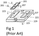
- FIG. 1 shows a known cascode HEMT semiconductor device.
- a HEMT die 221 is shown.
- the HEMT die comprises a HEMT source 223, a HEMT gate 225 and a HEMT drain 227.
- the HEMT gate 225 is diverted to the bottom of the HEMT die through vias 229.
- MOSFET metal-oxide-semiconductor field-effect transistor
- the MOSFET source 203 is connected to the HEMT gate 225.
- the known power device packages provide heat dissipation paths from both top and bottom surfaces of the package.
- the dual heat dissipation paths provide increased current density compared to conventional single dissipation path packages. This also provides an improved junction-to-ambient thermal impedance.
- the dual heat dissipation path packages can either handle more power or operate with a lower junction temperature.
- a lower junction temperature means a lower drain to source on-resistance. This provides a higher efficiency of the packaged component.
- a reduction in junction temperature means an increase in product reliability.
- the known semiconductor package structure comprises a connective bridge 11, a semiconductor device or electronic device 14, and a lead frame or conductive support structure 17.
- the semiconductor device 14 can be for a power MOSFET.
- Semiconductor device 14 is shown with a current carrying electrode 19 formed overlying a major surface 21, and a major surface 22 that includes second current carrying electrodes 23.
- Major surface 22 further includes a control electrode 24.
- the current carrying electrode 19 can be a drain electrode
- the current carrying electrodes 23 can be source electrodes
- the control electrode 24 corresponds can be a gate electrode of a MOSFET device.
- Conductive plate 11 and lead frame 17 comprise a conductive material.
- Plate 11 includes alignment structures 110 formed on or extending from a major surface 112 of plate 11. The alignment structures 110 are used for coupling as well. These are rectangular like blocks formed at the four corners of plate 11.
- Lead frame 17 comprises a plurality of portions or components 170, 171, 172, and 173.
- Pad portions 170 and 173 correspond to one current carrying electrode. They provide electrical contact between current carrying electrode 19 to an opposite surface of the structure shown in Figure 2 .
- the pad portions 170 and 173 correspond to drain contacts for the structure.
- Pad portions 170 and 173 are configured to include alignment features or portions 41. Alignment portions 41 are configured to receive the alignment structures 110 of plate 11. This provides a consistent alignment and planarity feature for the structure and planarity control of plate 11 with respect to semiconductor 14.
- Pad portion 172 is a gate electrode contact.
- the pad portion 172 includes an elevated contact portion or pedestal 272 configured or placed to couple with or bond to control electrode 24 of semiconductor device 14.
- Pad portion 171 is electrically coupled to the current carrying electrodes 23 of semiconductor device 14.
- Pad portions 170, 171, 172, and 173 are held together with a frame and tie bar portions, which are subsequently removed during the assembly process. These conventional structures are not shown in Figure 2 .
- Packaged semiconductor device comprises a heat dissipation path device because heat is dissipated out of both surfaces of the packaged semiconductor device. Specifically, heat is dissipated through plate 11 exposed at or on the upper surface, and through pad portions 170, 172, and 173 exposed on opposite, lower surface.
- portion 110 to portion 41 fully rely on how optimised the positional accuracy and tolerance for them to be fully integrated. Any miscalculation will impact coplanarity that will impact heat dissipation and power efficiency.
- a cascode HEMT semiconductor device comprises a lead frame, and a die pad attached to the lead frame.
- the cascode HEMT semiconductor device further comprises a first lateral silicon die, e.g. a HEMT die.
- the HEMT die attached to the die pad.
- the HEMT die comprises a HEMT source and a HEMT drain on its first side and a HEMT gate on its second side.
- the HEMT drain comprises a HEMT drain clip.
- the cascode HEMT semiconductor device further comprises a second lateral silicon die, e.g. a MOSFET die.
- the MOSFET die is attached to the source of the HEMT die.
- the MOSFET die comprises a MOSFET source, a MOSFET gate and a MOSFET drain.
- the MOSFET drain is connected to the HEMT source.
- the MOSFET source comprises a MOSFET source clip.
- the MOSFET source clip comprises at least one pillar that is arranged to connect the MOSFET source to the HEMT gate. This is established by connecting the pillar to the die pad, since the HEMT gate is connected to the die pad.
- connection between the pillar and the die pad i.e. the connection between the MOSFET source to the HEMT gate
- a conductive material is a solder, a paste, a sintering material, a welding, etc.
- a cascode HEMT semiconductor device is a gallium nitride (GaN) device.
- the pillars are 90 degrees pillars.
- the die pad comprises an indentation, wherein the indentation is arranged to avoid a direct contact between the die pad and the pillar.
- the contact is established by above mentioned conductive material.
- the indentation can be in any suitable size range, for example between 10-100 ⁇ m. In an embodiment of the invention the indentation is around 50 ⁇ m.
- the MOSFET source clip comprises multiple pillars so to connect the MOSFET source to the HEMT gate. This provides improved stability and reliability of the connection between the MOSFET source and the HEMT gate. Even if one (or more) of the pillars is disconnected, the connection between the MOSFET source and the HEMT gate will exist as long as at least one of the pillars is connected to the die pad.
- the die pad comprises a separate indentation for each of the multiple pillars. This arrangement provides improved stability and reliability.
- an automotive part comprises a cascode HEMT semiconductor device as specified in any of the previous embodiments above.
- An embodiment of this invention relates to a method of forming a cascode HEMT semiconductor device.
- the method comprises the following steps. Forming a die pad with an indentation. Apply a first solder, or any conductive material, on the die pad for a HEMT die and for a pillar of a MOSFET source clip of a MOSFET die.
- Attach the HEMT die Apply a second solder, or any conductive material, on top of the HEMT die for a HEMT source and HEMT drain, wherein a HEMT gate is diverted at the back of the HEMT die.
- a MOSFET source and a MOSFET gate are provided on the top of the MOSFET die.
- a MOSFET drain is provided at the bottom of the MOSFET die. The MOSFET drain is attached to the HEMT source. Apply a third solder, or any conductive material, on the top of the MOSFET die for the MOSFET source and the MOSFET gate.
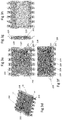
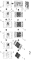
- Figures 3a-h illustrate a cascode HEMT semiconductor device according to embodiments. These figures illustrate the cascade HEMT semiconductor device from different view angles.
- the device comprises a lead frame 241, wherein a HEMT die 221 is attached on the lead frame 241.
- a matrix of die pad is attached to the lead frame 241.
- the HEMT die comprises a HEMT source 223, a HEMT gate 225 and a HEMT drain 227.
- the HEMT gate 225 is diverted to the bottom of the HEMT die through vias 229.
- the HEMT gate 225 is connected to the die pad 243.
- the HEMT drain 227 comprises a HEMT drain clip 228.
- the HEMT drain clip 228 is used to create external leads, also called terminals, for the HEMT drain connection.
- a MOSFET die 201 comprises a MOSFET source 203, a MOSFET gate 205 and a MOSFET drain 207.
- the MOSFET die 201 is arranged on the HEMT die 221 so that the MOSFET drain 207 is connected to the HEMT source 223 as shown in Figure 3g .
- the MOSFET source 203 comprises a MOSFET source clip 204 as shown in Figures 3a, 3b and 3c .
- the MOSFET source clip 204 comprises one or more pillars 209 as shown in Figures 3a and 3b . These pillars 209 are arranged to connect the MOSFET source 203 to the HEMT gate 225.
- the connection between the MOSFET source 203, via the MOSFET source clip 204 and the pillars 209, to the HEMT gate 225 is established by a conductive material 245, as shown in the Figure 3b .
- the conductive material 245 can be any conductive adhesive, such as a solder, a paste, a sintering material, a welding, etc.
- a MOSFET die is described.
- it can be also any other semiconductor device such as a power MOSFET, insulated gate bipolar transistor, a bipolar transistor, a JFET device, a MESFET device, a thyristor, a diode, or the like.
- a cascode HEMT semiconductor device can be a gallium nitride (GaN) device, a clip bonded product, a half bridge GaN product, or a product with a dual cascode inside a package, or any similar product.
- GaN gallium nitride
- the innovation is applicable to all semiconductor packages using clip as interconnects that are integrated to leads or internal clips.
- a cascode HEMT semiconductor device wherein one of the embodiments is described above and shown in Figures 3a-h , the usage of pillars 209 will improve the thermal performance of the device by providing a path for the heat to spread between the top and the bottom of the device, before being removed from the device through the base or the leads.
- such a cascode HEMT semiconductor device wherein one of the embodiments is described above and shown in Figures 3a-h , is arranged to reduce the parasitic inductance and resistance of the package, compared to the known packages, through the use of clips and multiple pillars connected to the die pad 243, which is acting as a heatsink.
- Usage of multiple pillars 209 provides that a cascode HEMT semiconductor device will be more reliable. Even in case that one of the pillars 209 is disconnected from the die pad 243, the connection will still be established if at least one of the pillars 209 is connected, i.e. it will not result to an open circuit.
- the reliability of a cascode HEMT semiconductor device will be further improved by the addition of an indentation on the die pad, or a gap in between the pillars and the die pad.
- the indentation can be about 10-100 ⁇ m, preferably about 50 ⁇ m.
- the gap can be for example between 10-50 ⁇ m. This is designed so that the pillars 209 not to touch the die pad. By avoiding the pillars touching the die pad, the probability of an open connection between the HEMT drain clip 228 or the MOSFET source clip 204 is reduced during a moulding process.
- the pillars can be about 90 degrees pillars.
- the connection of the pillars 209 to the die pad can be done with or without the use of an indentation on the die pad 243 at the point where the pillars 209 connect to the die pad 243, as long as there is a 10-50 ⁇ m gap in between pillars 209 and die pad 243 for a conductive material 245, e.g. a conductive adhesive.
- the pillars 209 are arranged to improve parasitic and thermal performance of a cascode HEMT semiconductor device as it will distribute or spread electrical and thermal towards the bottom heatsink faster.
- Such a design can be applied on a gull wing and other very cost-effective materials.
- Such a design has no limitation on creepage and clearance.
- Figures 4a-d illustrate an embodiment of the invention wherein a cascode HEMT semiconductor device after singulation is shown.
- Figure 5 illustrates process flow steps for forming a cascode HEMT semiconductor device according to an embodiment of the invention.
- the process flow comprises the steps:
Landscapes
- Junction Field-Effect Transistors (AREA)
Abstract
Description
- The present invention relates to a cascode high electron mobility (HEMT) semiconductor device a method of forming a cascode HEMT semiconductor device. The invention also relates to a leadless packaged semiconductor device.
-
Figure 1 shows a known cascode HEMT semiconductor device. A HEMT die 221 is shown. The HEMT die comprises aHEMT source 223, a HEMTgate 225 and a HEMTdrain 227. The HEMTgate 225 is diverted to the bottom of the HEMT die throughvias 229. - A metal-oxide-semiconductor field-effect transistor (MOSFET) die 201 is shown in
Figure 1 . The MOSFET die comprises aMOSFET source 203, aMOSFET gate 205 and aMOSFET drain 207. TheMOSFET drain 207 is connected to the HEMTsource 223. - Although not shown in
Figure 1 , theMOSFET source 203 is connected to the HEMTgate 225. - One of the main challenges in the packaging of semiconductor components, such as power semiconductor devices, is the heat dissipation. Examples of prior art power packages that have been developed and improved upon to address such issues include the TO-220, TO-218, CASE 77, TO-247, Dpak, D2pak, D3pak, quad flat pack no-lead (QFN), quad flat pack (QFP), small outline (SOP) packages among others.
- The known power device packages provide heat dissipation paths from both top and bottom surfaces of the package. In this case the dual heat dissipation paths provide increased current density compared to conventional single dissipation path packages. This also provides an improved junction-to-ambient thermal impedance. Compared to single heat dissipation path packages, the dual heat dissipation path packages can either handle more power or operate with a lower junction temperature. In case of MOSFET devices, a lower junction temperature means a lower drain to source on-resistance. This provides a higher efficiency of the packaged component. A reduction in junction temperature means an increase in product reliability.
- A semiconductor package structure having multiple heat dissipation paths is described in
US20080054438A1 patent. This package structure is shown inFigure 2 . - The known semiconductor package structure comprises a connective bridge 11, a semiconductor device or
electronic device 14, and a lead frame orconductive support structure 17. Thesemiconductor device 14 can be for a power MOSFET.Semiconductor device 14 is shown with a current carrying electrode 19 formed overlying a major surface 21, and amajor surface 22 that includes second current carryingelectrodes 23.Major surface 22 further includes acontrol electrode 24. The current carrying electrode 19 can be a drain electrode, the current carryingelectrodes 23 can be source electrodes, and thecontrol electrode 24 corresponds can be a gate electrode of a MOSFET device. - Conductive plate 11 and
lead frame 17 comprise a conductive material. Plate 11 includesalignment structures 110 formed on or extending from amajor surface 112 of plate 11. Thealignment structures 110 are used for coupling as well. These are rectangular like blocks formed at the four corners of plate 11. -
Lead frame 17 comprises a plurality of portions orcomponents Pad portions Figure 2 . Thepad portions Pad portions alignment structures 110 of plate 11. This provides a consistent alignment and planarity feature for the structure and planarity control of plate 11 with respect tosemiconductor 14. -
Pad portion 172 is a gate electrode contact. Thepad portion 172 includes an elevated contact portion orpedestal 272 configured or placed to couple with or bond to controlelectrode 24 ofsemiconductor device 14. -
Pad portion 171 is electrically coupled to the current carryingelectrodes 23 ofsemiconductor device 14.Pad portions Figure 2 . - Packaged semiconductor device comprises a heat dissipation path device because heat is dissipated out of both surfaces of the packaged semiconductor device. Specifically, heat is dissipated through plate 11 exposed at or on the upper surface, and through
pad portions - The disadvantage of prior art is that the coupling of
portion 110 to portion 41 fully rely on how optimised the positional accuracy and tolerance for them to be fully integrated. Any miscalculation will impact coplanarity that will impact heat dissipation and power efficiency. - Various example embodiments are directed to the disadvantage as described above and/or others which may become apparent from the following disclosure.
- According to an embodiment of this invention a cascode HEMT semiconductor device comprises a lead frame, and a die pad attached to the lead frame.
- The cascode HEMT semiconductor device further comprises a first lateral silicon die, e.g. a HEMT die. The HEMT die attached to the die pad. The HEMT die comprises a HEMT source and a HEMT drain on its first side and a HEMT gate on its second side. The HEMT drain comprises a HEMT drain clip.
- The cascode HEMT semiconductor device further comprises a second lateral silicon die, e.g. a MOSFET die. The MOSFET die is attached to the source of the HEMT die. The MOSFET die comprises a MOSFET source, a MOSFET gate and a MOSFET drain. The MOSFET drain is connected to the HEMT source. The MOSFET source comprises a MOSFET source clip. The MOSFET source clip comprises at least one pillar that is arranged to connect the MOSFET source to the HEMT gate. This is established by connecting the pillar to the die pad, since the HEMT gate is connected to the die pad.
- In an embodiment of the invention the connection between the pillar and the die pad, i.e. the connection between the MOSFET source to the HEMT gate, is not direct, but it is established by a conductive material. Some of the examples of such a conductive material are a solder, a paste, a sintering material, a welding, etc.
- According to an embodiment of this invention a cascode HEMT semiconductor device is a gallium nitride (GaN) device.
- According to an embodiment of this invention the pillars are 90 degrees pillars.
- According to an embodiment of this invention the die pad comprises an indentation, wherein the indentation is arranged to avoid a direct contact between the die pad and the pillar. The contact is established by above mentioned conductive material.
- The indentation can be in any suitable size range, for example between 10-100µm. In an embodiment of the invention the indentation is around 50µm.
- According to an embodiment of this invention the MOSFET source clip comprises multiple pillars so to connect the MOSFET source to the HEMT gate. This provides improved stability and reliability of the connection between the MOSFET source and the HEMT gate. Even if one (or more) of the pillars is disconnected, the connection between the MOSFET source and the HEMT gate will exist as long as at least one of the pillars is connected to the die pad.
- According to an embodiment of this invention the die pad comprises a separate indentation for each of the multiple pillars. This arrangement provides improved stability and reliability.
- According to an embodiment of this invention an automotive part comprises a cascode HEMT semiconductor device as specified in any of the previous embodiments above.
- An embodiment of this invention relates to a method of forming a cascode HEMT semiconductor device. The method comprises the following steps. Forming a die pad with an indentation. Apply a first solder, or any conductive material, on the die pad for a HEMT die and for a pillar of a MOSFET source clip of a MOSFET die.
- Attach the HEMT die. Apply a second solder, or any conductive material, on top of the HEMT die for a HEMT source and HEMT drain, wherein a HEMT gate is diverted at the back of the HEMT die.
- Attach the MOSFET die. A MOSFET source and a MOSFET gate are provided on the top of the MOSFET die. A MOSFET drain is provided at the bottom of the MOSFET die. The MOSFET drain is attached to the HEMT source. Apply a third solder, or any conductive material, on the top of the MOSFET die for the MOSFET source and the MOSFET gate.
- Form a HEMT drain clip for the HEMT drain. Form the MOSFET source clip for the MOSFET source. Form a MOSFET gate clip for the MOSFET gate.
- Connect the MOSFET source clip to the indentation of the die pad using a conductive material. In this way the connection between the MOSFET source and the HEMT gate is established.
- Further semiconductor device production typical steps are executed. Moulding for all units so to encapsulate the silicon. This encapsulation is required to protect the silicon dies from any oxidation and contamination. The plating step for the units. In this way it will plate any exposed copper in an assembled unit. This enables that the product can be soldered on a printed circuit board (PCB) footprint. Also, the Cu contamination is avoided. The dambar will be further removed so that the leads will become independent terminals of the package. The leads will be cut and trimmed. Gull wing leads for surface mounting will be formed. On the end the singulation of units will be done by cutting the side tie bars. The tie bars are the only part of lead frame that holds the unit after all steps.
- So that the manner in which the features of the present disclosure can be understood in detail, a more particular description is made with reference to embodiments, some of which are illustrated in the appended figures. It is to be noted, however, that the appended figures illustrate only typical embodiments and are therefore not to be considered limiting of its scope. The figures are for facilitating an understanding of the disclosure and thus are not necessarily drawn to scale. Advantages of the subject matter claimed will become apparent to those skilled in the art upon reading this description in conjunction with the accompanying figures, in which like reference numerals have been used to designate like elements, and in which:
-
Figure 1 shows a known cascode HEMT semiconductor device; -
Figure 2 shows a known semiconductor package structure having multiple heat dissipation paths; -
Figures 3a-h illustrate a cascode HEMT semiconductor device according to embodiments; -
Figures 4a-d illustrate a cascode HEMT semiconductor device according to embodiments after singulation; -
Figure 5 illustrates process flow steps for forming a cascode HEMT semiconductor device according to embodiments; - In the figures and the following description like reference numerals refer to like features.
Figures 3a-h illustrate a cascode HEMT semiconductor device according to embodiments. These figures illustrate the cascade HEMT semiconductor device from different view angles. - The device comprises a
lead frame 241, wherein aHEMT die 221 is attached on thelead frame 241. In an embodiment of the invention a matrix of die pad is attached to thelead frame 241. The HEMT die comprises aHEMT source 223, aHEMT gate 225 and aHEMT drain 227. TheHEMT gate 225 is diverted to the bottom of the HEMT die throughvias 229. TheHEMT gate 225 is connected to thedie pad 243. TheHEMT drain 227 comprises aHEMT drain clip 228. TheHEMT drain clip 228 is used to create external leads, also called terminals, for the HEMT drain connection. - A MOSFET die 201 comprises a
MOSFET source 203, aMOSFET gate 205 and aMOSFET drain 207. The MOSFET die 201 is arranged on the HEMT die 221 so that theMOSFET drain 207 is connected to theHEMT source 223 as shown inFigure 3g . - The
MOSFET source 203 comprises aMOSFET source clip 204 as shown inFigures 3a, 3b and 3c . TheMOSFET source clip 204 comprises one ormore pillars 209 as shown inFigures 3a and 3b . Thesepillars 209 are arranged to connect theMOSFET source 203 to theHEMT gate 225. The connection between theMOSFET source 203, via theMOSFET source clip 204 and thepillars 209, to theHEMT gate 225 is established by aconductive material 245, as shown in theFigure 3b . Theconductive material 245 can be any conductive adhesive, such as a solder, a paste, a sintering material, a welding, etc. - This arrangement, wherein the
MOSFET source clip 204 is connected to thedie pad 243 using one ormore pillars 209, secures that the connection to thedie pad 243 is improved with an indentation in thedie pad 243 at the point where thepillars 209 connect. Thus, there is no direct connection between thedie pad 243 andpillars 209. They are connected with each other via aconductive adhesive 245. Said indentation filled by the conductive adhesive is shown inFigure 3b . - In this embodiment of the invention, as an example, a MOSFET die is described. However, it can be also any other semiconductor device such as a power MOSFET, insulated gate bipolar transistor, a bipolar transistor, a JFET device, a MESFET device, a thyristor, a diode, or the like.
- A cascode HEMT semiconductor device can be a gallium nitride (GaN) device, a clip bonded product, a half bridge GaN product, or a product with a dual cascode inside a package, or any similar product.
- The innovation is applicable to all semiconductor packages using clip as interconnects that are integrated to leads or internal clips.
- A cascode HEMT semiconductor device, wherein one of the embodiments is described above and shown in
Figures 3a-h , the usage ofpillars 209 will improve the thermal performance of the device by providing a path for the heat to spread between the top and the bottom of the device, before being removed from the device through the base or the leads. - Moreover, such a cascode HEMT semiconductor device, wherein one of the embodiments is described above and shown in
Figures 3a-h , is arranged to reduce the parasitic inductance and resistance of the package, compared to the known packages, through the use of clips and multiple pillars connected to thedie pad 243, which is acting as a heatsink. - Usage of
multiple pillars 209 provides that a cascode HEMT semiconductor device will be more reliable. Even in case that one of thepillars 209 is disconnected from thedie pad 243, the connection will still be established if at least one of thepillars 209 is connected, i.e. it will not result to an open circuit. - The reliability of a cascode HEMT semiconductor device will be further improved by the addition of an indentation on the die pad, or a gap in between the pillars and the die pad. For example the indentation can be about 10-100µm, preferably about 50µm. The gap can be for example between 10-50µm. This is designed so that the
pillars 209 not to touch the die pad. By avoiding the pillars touching the die pad, the probability of an open connection between theHEMT drain clip 228 or theMOSFET source clip 204 is reduced during a moulding process. - The pillars can be about 90 degrees pillars. The connection of the
pillars 209 to the die pad can be done with or without the use of an indentation on thedie pad 243 at the point where thepillars 209 connect to thedie pad 243, as long as there is a 10-50µm gap in betweenpillars 209 and diepad 243 for aconductive material 245, e.g. a conductive adhesive. Thepillars 209 are arranged to improve parasitic and thermal performance of a cascode HEMT semiconductor device as it will distribute or spread electrical and thermal towards the bottom heatsink faster. - Such a design can be applied on a gull wing and other very cost-effective materials.
- Such a design has no limitation on creepage and clearance.
-
Figures 4a-d illustrate an embodiment of the invention wherein a cascode HEMT semiconductor device after singulation is shown. -
Figure 5 illustrates process flow steps for forming a cascode HEMT semiconductor device according to an embodiment of the invention. - The process flow comprises the steps:
- step 301: forming a
die pad 241 with or without indentation; - step 303: print, write or dispense a solder on
die pad 241;
∘ one big solder for aHEMT die 221 and multiple (e.g. four as in an example shown in step 303) single solders forpillars 209 of aMOSFET source clip 204; - step 305: attach a first lateral silicon die; in an embodiment of the invention a
HEMT die 221 is attached; the attaching on the printed solder can be done using die attach machine; - step 307: print, write or dispense a solder on top of the first lateral silicon die, in this example it is the HEMT die 221, for a
HEMT source 223 andHEMT drain 227; aHEMT gate 225 is diverted at the back of the HEMT die 221 for above explained functionality improvement purposes; - step 309: attach another silicon vertical die, in this case a
MOSFET die 201, wherein aMOSFET source 203 and aMOSFET gate 205 are located on the top, while aMOSFET drain 207 is located at the bottom of the MOSFET die 201; theMOSFET drain 207 is in this way attached to theHEMT source 223 of the HEMT die 221; this is done using another set of die attach machine arranged to connect theHEMT source 223 to theMOSFET drain 207; - step 311: print, write or dispense a solder on top of the second silicon die, in this example embodiment a MOSFET die, for a
MOSFET source 203 and aMOSFET gate 205; - step 313: providing a
HEMT drain clip 228 for theHEMT drain 227, and providing aMOSFET source clip 204 for theMOSFET source 203 together with aMOSFET gate clip 206 for theMOSFET gate 205; further, a reflow will be done for all units for solder curing; - step 315: perform moulding for all units so to encapsulate the silicon; an encapsulation is required to protect the silicon dies from any oxidation and contamination; further plating step for the units will be done, wherein it will plate any exposed copper (Cu) in an assembled unit; plating is required to ensure that the product can be soldered on a printed circuit board (PCB) footprint as well as to avoid Cu contamination;
- step 317: dambar cutting step will be executed, wherein it will remove the dambar connecting all leads together; consequently, the leads will become independent terminals of the package;
- step 319: cutting and trimming the leads;
- step 321: forming of gull wing leads for surface mounting; and
- step 323: singulation of units by cutting the side tie bars; the tie bars are the only part of lead frame that holds the unit after all processes.
- Particular and preferred aspects of the invention are set out in the accompanying independent claims. Combinations of features from the dependent and/or independent claims may be combined as appropriate and not merely as set out in the claims.
- The scope of the present disclosure includes any novel feature or combination of features disclosed therein either explicitly or implicitly or any generalisation thereof irrespective of whether or not it relates to the claimed invention or mitigate against any or all of the problems addressed by the present invention. The applicant hereby gives notice that new claims may be formulated to such features during prosecution of this application or of any such further application derived therefrom. In particular, with reference to the appended claims, features from dependent claims may be combined with those of the independent claims and features from respective independent claims may be combined in any appropriate manner and not merely in specific combinations enumerated in the claims.
- Features which are described in the context of separate embodiments may also be provided in combination in a single embodiment. Conversely, various features which are, for brevity, described in the context of a single embodiment, may also be provided separately or in any suitable sub combination.
- Term "comprising" does not exclude other elements or steps, the term "a" or "an" does not exclude a plurality. Reference signs in the claims shall not be construed as limiting the scope of the claims.
Claims (10)
- A cascode high electron mobility (HEMT) semiconductor device comprising:- a lead frame,- a die pad attached to the lead frame,- a HEMT die attached to the die pad, the HEMT die comprising:∘ a HEMT source and a HEMT drain on a first side,
▪ wherein the HEMT drain comprises a HEMT drain clip,∘ a HEMT gate on a second side,- a metal-oxide-semiconductor field-effect transistor (MOSFET) die attached to the source of the HEMT die, the MOSFET die comprising:
∘ a MOSFET source, a MOSFET gate and a MOSFET drain,- wherein the MOSFET drain is connected to the HEMT source,- wherein the MOSFET source comprises a MOSFET source clip,- wherein the MOSFET source clip comprises a pillar so to connect the MOSFET source to the HEMT gate,- wherein the connection between the MOSFET source to the HEMT gate is established by a conductive material. - A cascode HEMT semiconductor device as claimed in claim 1, wherein the device is a gallium nitride (GaN) device.
- A cascode HEMT semiconductor device as claimed in claim 1, wherein the pillar is a 90 degrees pillar.
- A cascode HEMT semiconductor device as claimed in claim 1, wherein the die pad comprises an indentation, wherein the indentation is configured to avoid a direct contact between the die pad and the pillar.
- A cascode HEMT semiconductor device as claimed in claim 4, wherein the indentation is in a range between 10-100µm, preferably around 50µm.
- A cascode HEMT semiconductor device as claimed in any of the previous claims, wherein the MOSFET source clip comprises multiple pillars so to connect the MOSFET source to the HEMT gate.
- A cascode HEMT semiconductor device as claimed in claim 6, wherein the die pad comprises a separate indentation for each of the multiple pillars.
- An automotive part comprising a cascode HEMT semiconductor device as specified in any of the previous claims.
- A method of forming a semiconductor device as specified in any of the previous claims.
- A method of forming a cascode HEMT semiconductor device, the method comprising steps:- forming a die pad with an indentation;- apply a first conductive material on the die pad for a HEMT die and for a pillar of a MOSFET source clip of a MOSFET die;- attach the HEMT die;- apply a second conductive material on top of the HEMT die for a HEMT source and HEMT drain, wherein a HEMT gate is diverted at the back of the HEMT die;- attach the MOSFET die, wherein a MOSFET source and a MOSFET gate are provided on the top of the MOSFET die, and wherein a MOSFET drain is provided at the bottom of the MOSFET die
∘ wherein the MOSFET drain is attached to the HEMT source;- apply a third conductive material on the top of the MOSFET die for the MOSFET source and the MOSFET gate;- form a HEMT drain clip for the HEMT drain, form the MOSFET source clip for the MOSFET source, and form a MOSFET gate clip for the MOSFET gate;- connect the MOSFET source clip to the indentation using a conductive material, wherein the connection between the MOSFET source and the HEMT gate is established;- encapsulate the device;- dambar cutting of the device so that independent leads are formed;- cutting and trimming the leads;- forming of gull wing leads; and- singulation.
Priority Applications (4)
| Application Number | Priority Date | Filing Date | Title |
|---|---|---|---|
| EP20163929.1A EP3882969B1 (en) | 2020-03-18 | 2020-03-18 | A cascode semiconductor device and method of manufacture |
| CN202011589335.3A CN113496977B (en) | 2020-03-18 | 2020-12-29 | Cascode semiconductor device and method of manufacture |
| US17/204,438 US11538744B2 (en) | 2020-03-18 | 2021-03-17 | Cascode semiconductor |
| US18/086,147 US12293961B2 (en) | 2020-03-18 | 2022-12-21 | Method of manufacture for a cascode semiconductor device |
Applications Claiming Priority (1)
| Application Number | Priority Date | Filing Date | Title |
|---|---|---|---|
| EP20163929.1A EP3882969B1 (en) | 2020-03-18 | 2020-03-18 | A cascode semiconductor device and method of manufacture |
Publications (2)
| Publication Number | Publication Date |
|---|---|
| EP3882969A1 true EP3882969A1 (en) | 2021-09-22 |
| EP3882969B1 EP3882969B1 (en) | 2024-05-01 |
Family
ID=69846233
Family Applications (1)
| Application Number | Title | Priority Date | Filing Date |
|---|---|---|---|
| EP20163929.1A Active EP3882969B1 (en) | 2020-03-18 | 2020-03-18 | A cascode semiconductor device and method of manufacture |
Country Status (3)
| Country | Link |
|---|---|
| US (2) | US11538744B2 (en) |
| EP (1) | EP3882969B1 (en) |
| CN (1) | CN113496977B (en) |
Families Citing this family (4)
| Publication number | Priority date | Publication date | Assignee | Title |
|---|---|---|---|---|
| US12487254B2 (en) * | 2021-08-23 | 2025-12-02 | Allegro Microsystems, Llc | Packaged current sensor integrated circuit |
| EP4167286A1 (en) * | 2021-10-14 | 2023-04-19 | Nexperia B.V. | A stacked semiconductor assembly |
| CN114520214B (en) * | 2022-02-11 | 2026-03-06 | 深圳市时代速信科技有限公司 | A common-source cascode transistor package structure |
| EP4340021A1 (en) * | 2022-09-16 | 2024-03-20 | Nexperia B.V. | Reduced stress clip for semiconductor die |
Citations (3)
| Publication number | Priority date | Publication date | Assignee | Title |
|---|---|---|---|---|
| US20080054438A1 (en) | 2006-08-30 | 2008-03-06 | Semiconductor Components Industries, Llc | Semiconductor package structure having multiple heat dissipation paths and method of manufacture |
| US20150001692A1 (en) * | 2013-06-28 | 2015-01-01 | Delta Electronics, Inc. | Semiconductor component having a lateral semiconductor device and a vertical semiconductor device |
| JP2015056564A (en) * | 2013-09-12 | 2015-03-23 | 古河電気工業株式会社 | Semiconductor device and manufacturing method thereof |
Family Cites Families (4)
| Publication number | Priority date | Publication date | Assignee | Title |
|---|---|---|---|---|
| US6777800B2 (en) * | 2002-09-30 | 2004-08-17 | Fairchild Semiconductor Corporation | Semiconductor die package including drain clip |
| US8164199B2 (en) * | 2009-07-31 | 2012-04-24 | Alpha and Omega Semiconductor Incorporation | Multi-die package |
| JP5970316B2 (en) * | 2012-09-26 | 2016-08-17 | ルネサスエレクトロニクス株式会社 | Manufacturing method of semiconductor device |
| US9443787B2 (en) * | 2013-08-09 | 2016-09-13 | Infineon Technologies Austria Ag | Electronic component and method |
-
2020
- 2020-03-18 EP EP20163929.1A patent/EP3882969B1/en active Active
- 2020-12-29 CN CN202011589335.3A patent/CN113496977B/en active Active
-
2021
- 2021-03-17 US US17/204,438 patent/US11538744B2/en active Active
-
2022
- 2022-12-21 US US18/086,147 patent/US12293961B2/en active Active
Patent Citations (3)
| Publication number | Priority date | Publication date | Assignee | Title |
|---|---|---|---|---|
| US20080054438A1 (en) | 2006-08-30 | 2008-03-06 | Semiconductor Components Industries, Llc | Semiconductor package structure having multiple heat dissipation paths and method of manufacture |
| US20150001692A1 (en) * | 2013-06-28 | 2015-01-01 | Delta Electronics, Inc. | Semiconductor component having a lateral semiconductor device and a vertical semiconductor device |
| JP2015056564A (en) * | 2013-09-12 | 2015-03-23 | 古河電気工業株式会社 | Semiconductor device and manufacturing method thereof |
Also Published As
| Publication number | Publication date |
|---|---|
| US20230123782A1 (en) | 2023-04-20 |
| CN113496977B (en) | 2024-01-30 |
| CN113496977A (en) | 2021-10-12 |
| US11538744B2 (en) | 2022-12-27 |
| US20210296218A1 (en) | 2021-09-23 |
| EP3882969B1 (en) | 2024-05-01 |
| US12293961B2 (en) | 2025-05-06 |
Similar Documents
| Publication | Publication Date | Title |
|---|---|---|
| US12293961B2 (en) | Method of manufacture for a cascode semiconductor device | |
| TWI450373B (en) | Double-sided cooling integrated power device package and module, and manufacturing method | |
| US9196577B2 (en) | Semiconductor packaging arrangement | |
| US8008759B2 (en) | Pre-molded clip structure | |
| CN101136380B (en) | Semiconductor package structure having multiple heat dissipation paths and method of manufacture | |
| US11574855B2 (en) | Package with dies mounted on opposing surfaces of a leadframe | |
| US9099441B2 (en) | Power transistor arrangement and method for manufacturing the same | |
| US10825753B2 (en) | Semiconductor device and method of manufacture | |
| US11227819B2 (en) | Cascode semiconductor device and method of manufacture | |
| US10879155B2 (en) | Electronic device with double-sided cooling | |
| CN107148671A (en) | Triple Stack Semiconductor Package | |
| TWI452662B (en) | Bilateral cooling integrated power supply device package and module and manufacturing method | |
| JP2024505028A (en) | Packaged electronic device with substrate with thermally conductive adhesive layer | |
| CN114864528A (en) | Semiconductor device and method for manufacturing semiconductor device | |
| CN114899170A (en) | 4-pin TO-247 packaging structure for power gallium nitride HEMT device | |
| EP2973690B1 (en) | Stack die package | |
| CN112635411A (en) | Semiconductor package with top or bottom side cooling | |
| CN111244061A (en) | Packaging structure of gallium nitride equipment | |
| CN111987050A (en) | Semiconductor package with space-saving lead and die pad design | |
| CN116525559A (en) | Semiconductor device package with integral heat sink | |
| CN121666900A (en) | Semiconductor device package with integral heat dissipation structure |
Legal Events
| Date | Code | Title | Description |
|---|---|---|---|
| PUAI | Public reference made under article 153(3) epc to a published international application that has entered the european phase |
Free format text: ORIGINAL CODE: 0009012 |
|
| STAA | Information on the status of an ep patent application or granted ep patent |
Free format text: STATUS: THE APPLICATION HAS BEEN PUBLISHED |
|
| AK | Designated contracting states |
Kind code of ref document: A1 Designated state(s): AL AT BE BG CH CY CZ DE DK EE ES FI FR GB GR HR HU IE IS IT LI LT LU LV MC MK MT NL NO PL PT RO RS SE SI SK SM TR |
|
| STAA | Information on the status of an ep patent application or granted ep patent |
Free format text: STATUS: REQUEST FOR EXAMINATION WAS MADE |
|
| 17P | Request for examination filed |
Effective date: 20220321 |
|
| RBV | Designated contracting states (corrected) |
Designated state(s): AL AT BE BG CH CY CZ DE DK EE ES FI FR GB GR HR HU IE IS IT LI LT LU LV MC MK MT NL NO PL PT RO RS SE SI SK SM TR |
|
| GRAP | Despatch of communication of intention to grant a patent |
Free format text: ORIGINAL CODE: EPIDOSNIGR1 |
|
| STAA | Information on the status of an ep patent application or granted ep patent |
Free format text: STATUS: GRANT OF PATENT IS INTENDED |
|
| RIC1 | Information provided on ipc code assigned before grant |
Ipc: H01L 23/48 20060101ALI20231130BHEP Ipc: H01L 23/495 20060101ALI20231130BHEP Ipc: H01L 21/98 20060101ALI20231130BHEP Ipc: H01L 25/18 20060101AFI20231130BHEP |
|
| INTG | Intention to grant announced |
Effective date: 20231213 |
|
| RIN1 | Information on inventor provided before grant (corrected) |
Inventor name: ROSILLO, ADAM Inventor name: MONTGOMERY, ROBERT Inventor name: YANDOC, RICARDO |
|
| GRAS | Grant fee paid |
Free format text: ORIGINAL CODE: EPIDOSNIGR3 |
|
| GRAA | (expected) grant |
Free format text: ORIGINAL CODE: 0009210 |
|
| STAA | Information on the status of an ep patent application or granted ep patent |
Free format text: STATUS: THE PATENT HAS BEEN GRANTED |
|
| AK | Designated contracting states |
Kind code of ref document: B1 Designated state(s): AL AT BE BG CH CY CZ DE DK EE ES FI FR GB GR HR HU IE IS IT LI LT LU LV MC MK MT NL NO PL PT RO RS SE SI SK SM TR |
|
| REG | Reference to a national code |
Ref country code: GB Ref legal event code: FG4D |
|
| REG | Reference to a national code |
Ref country code: CH Ref legal event code: EP |
|
| REG | Reference to a national code |
Ref country code: IE Ref legal event code: FG4D |
|
| REG | Reference to a national code |
Ref country code: DE Ref legal event code: R096 Ref document number: 602020029906 Country of ref document: DE |
|
| REG | Reference to a national code |
Ref country code: LT Ref legal event code: MG9D |
|
| REG | Reference to a national code |
Ref country code: NL Ref legal event code: MP Effective date: 20240501 |
|
| PG25 | Lapsed in a contracting state [announced via postgrant information from national office to epo] |
Ref country code: IS Free format text: LAPSE BECAUSE OF FAILURE TO SUBMIT A TRANSLATION OF THE DESCRIPTION OR TO PAY THE FEE WITHIN THE PRESCRIBED TIME-LIMIT Effective date: 20240901 |
|
| PG25 | Lapsed in a contracting state [announced via postgrant information from national office to epo] |
Ref country code: BG Free format text: LAPSE BECAUSE OF FAILURE TO SUBMIT A TRANSLATION OF THE DESCRIPTION OR TO PAY THE FEE WITHIN THE PRESCRIBED TIME-LIMIT Effective date: 20240501 |
|
| PG25 | Lapsed in a contracting state [announced via postgrant information from national office to epo] |
Ref country code: HR Free format text: LAPSE BECAUSE OF FAILURE TO SUBMIT A TRANSLATION OF THE DESCRIPTION OR TO PAY THE FEE WITHIN THE PRESCRIBED TIME-LIMIT Effective date: 20240501 Ref country code: FI Free format text: LAPSE BECAUSE OF FAILURE TO SUBMIT A TRANSLATION OF THE DESCRIPTION OR TO PAY THE FEE WITHIN THE PRESCRIBED TIME-LIMIT Effective date: 20240501 |
|
| PG25 | Lapsed in a contracting state [announced via postgrant information from national office to epo] |
Ref country code: GR Free format text: LAPSE BECAUSE OF FAILURE TO SUBMIT A TRANSLATION OF THE DESCRIPTION OR TO PAY THE FEE WITHIN THE PRESCRIBED TIME-LIMIT Effective date: 20240802 |
|
| PG25 | Lapsed in a contracting state [announced via postgrant information from national office to epo] |
Ref country code: PT Free format text: LAPSE BECAUSE OF FAILURE TO SUBMIT A TRANSLATION OF THE DESCRIPTION OR TO PAY THE FEE WITHIN THE PRESCRIBED TIME-LIMIT Effective date: 20240902 |
|
| REG | Reference to a national code |
Ref country code: AT Ref legal event code: MK05 Ref document number: 1683613 Country of ref document: AT Kind code of ref document: T Effective date: 20240501 |
|
| PG25 | Lapsed in a contracting state [announced via postgrant information from national office to epo] |
Ref country code: NL Free format text: LAPSE BECAUSE OF FAILURE TO SUBMIT A TRANSLATION OF THE DESCRIPTION OR TO PAY THE FEE WITHIN THE PRESCRIBED TIME-LIMIT Effective date: 20240501 |
|
| PG25 | Lapsed in a contracting state [announced via postgrant information from national office to epo] |
Ref country code: ES Free format text: LAPSE BECAUSE OF FAILURE TO SUBMIT A TRANSLATION OF THE DESCRIPTION OR TO PAY THE FEE WITHIN THE PRESCRIBED TIME-LIMIT Effective date: 20240501 |
|
| PG25 | Lapsed in a contracting state [announced via postgrant information from national office to epo] |
Ref country code: AT Free format text: LAPSE BECAUSE OF FAILURE TO SUBMIT A TRANSLATION OF THE DESCRIPTION OR TO PAY THE FEE WITHIN THE PRESCRIBED TIME-LIMIT Effective date: 20240501 |
|
| PG25 | Lapsed in a contracting state [announced via postgrant information from national office to epo] |
Ref country code: PL Free format text: LAPSE BECAUSE OF FAILURE TO SUBMIT A TRANSLATION OF THE DESCRIPTION OR TO PAY THE FEE WITHIN THE PRESCRIBED TIME-LIMIT Effective date: 20240501 |
|
| PG25 | Lapsed in a contracting state [announced via postgrant information from national office to epo] |
Ref country code: LV Free format text: LAPSE BECAUSE OF FAILURE TO SUBMIT A TRANSLATION OF THE DESCRIPTION OR TO PAY THE FEE WITHIN THE PRESCRIBED TIME-LIMIT Effective date: 20240501 |
|
| PG25 | Lapsed in a contracting state [announced via postgrant information from national office to epo] |
Ref country code: PT Free format text: LAPSE BECAUSE OF FAILURE TO SUBMIT A TRANSLATION OF THE DESCRIPTION OR TO PAY THE FEE WITHIN THE PRESCRIBED TIME-LIMIT Effective date: 20240902 Ref country code: PL Free format text: LAPSE BECAUSE OF FAILURE TO SUBMIT A TRANSLATION OF THE DESCRIPTION OR TO PAY THE FEE WITHIN THE PRESCRIBED TIME-LIMIT Effective date: 20240501 Ref country code: NO Free format text: LAPSE BECAUSE OF FAILURE TO SUBMIT A TRANSLATION OF THE DESCRIPTION OR TO PAY THE FEE WITHIN THE PRESCRIBED TIME-LIMIT Effective date: 20240801 Ref country code: NL Free format text: LAPSE BECAUSE OF FAILURE TO SUBMIT A TRANSLATION OF THE DESCRIPTION OR TO PAY THE FEE WITHIN THE PRESCRIBED TIME-LIMIT Effective date: 20240501 Ref country code: LV Free format text: LAPSE BECAUSE OF FAILURE TO SUBMIT A TRANSLATION OF THE DESCRIPTION OR TO PAY THE FEE WITHIN THE PRESCRIBED TIME-LIMIT Effective date: 20240501 Ref country code: IS Free format text: LAPSE BECAUSE OF FAILURE TO SUBMIT A TRANSLATION OF THE DESCRIPTION OR TO PAY THE FEE WITHIN THE PRESCRIBED TIME-LIMIT Effective date: 20240901 Ref country code: HR Free format text: LAPSE BECAUSE OF FAILURE TO SUBMIT A TRANSLATION OF THE DESCRIPTION OR TO PAY THE FEE WITHIN THE PRESCRIBED TIME-LIMIT Effective date: 20240501 Ref country code: GR Free format text: LAPSE BECAUSE OF FAILURE TO SUBMIT A TRANSLATION OF THE DESCRIPTION OR TO PAY THE FEE WITHIN THE PRESCRIBED TIME-LIMIT Effective date: 20240802 Ref country code: FI Free format text: LAPSE BECAUSE OF FAILURE TO SUBMIT A TRANSLATION OF THE DESCRIPTION OR TO PAY THE FEE WITHIN THE PRESCRIBED TIME-LIMIT Effective date: 20240501 Ref country code: ES Free format text: LAPSE BECAUSE OF FAILURE TO SUBMIT A TRANSLATION OF THE DESCRIPTION OR TO PAY THE FEE WITHIN THE PRESCRIBED TIME-LIMIT Effective date: 20240501 Ref country code: BG Free format text: LAPSE BECAUSE OF FAILURE TO SUBMIT A TRANSLATION OF THE DESCRIPTION OR TO PAY THE FEE WITHIN THE PRESCRIBED TIME-LIMIT Effective date: 20240501 Ref country code: AT Free format text: LAPSE BECAUSE OF FAILURE TO SUBMIT A TRANSLATION OF THE DESCRIPTION OR TO PAY THE FEE WITHIN THE PRESCRIBED TIME-LIMIT Effective date: 20240501 Ref country code: RS Free format text: LAPSE BECAUSE OF FAILURE TO SUBMIT A TRANSLATION OF THE DESCRIPTION OR TO PAY THE FEE WITHIN THE PRESCRIBED TIME-LIMIT Effective date: 20240801 |
|
| PG25 | Lapsed in a contracting state [announced via postgrant information from national office to epo] |
Ref country code: DK Free format text: LAPSE BECAUSE OF FAILURE TO SUBMIT A TRANSLATION OF THE DESCRIPTION OR TO PAY THE FEE WITHIN THE PRESCRIBED TIME-LIMIT Effective date: 20240501 |
|
| PG25 | Lapsed in a contracting state [announced via postgrant information from national office to epo] |
Ref country code: EE Free format text: LAPSE BECAUSE OF FAILURE TO SUBMIT A TRANSLATION OF THE DESCRIPTION OR TO PAY THE FEE WITHIN THE PRESCRIBED TIME-LIMIT Effective date: 20240501 |
|
| PG25 | Lapsed in a contracting state [announced via postgrant information from national office to epo] |
Ref country code: CZ Free format text: LAPSE BECAUSE OF FAILURE TO SUBMIT A TRANSLATION OF THE DESCRIPTION OR TO PAY THE FEE WITHIN THE PRESCRIBED TIME-LIMIT Effective date: 20240501 |
|
| PG25 | Lapsed in a contracting state [announced via postgrant information from national office to epo] |
Ref country code: RO Free format text: LAPSE BECAUSE OF FAILURE TO SUBMIT A TRANSLATION OF THE DESCRIPTION OR TO PAY THE FEE WITHIN THE PRESCRIBED TIME-LIMIT Effective date: 20240501 Ref country code: SK Free format text: LAPSE BECAUSE OF FAILURE TO SUBMIT A TRANSLATION OF THE DESCRIPTION OR TO PAY THE FEE WITHIN THE PRESCRIBED TIME-LIMIT Effective date: 20240501 |
|
| PG25 | Lapsed in a contracting state [announced via postgrant information from national office to epo] |
Ref country code: SM Free format text: LAPSE BECAUSE OF FAILURE TO SUBMIT A TRANSLATION OF THE DESCRIPTION OR TO PAY THE FEE WITHIN THE PRESCRIBED TIME-LIMIT Effective date: 20240501 |
|
| PG25 | Lapsed in a contracting state [announced via postgrant information from national office to epo] |
Ref country code: SM Free format text: LAPSE BECAUSE OF FAILURE TO SUBMIT A TRANSLATION OF THE DESCRIPTION OR TO PAY THE FEE WITHIN THE PRESCRIBED TIME-LIMIT Effective date: 20240501 Ref country code: SK Free format text: LAPSE BECAUSE OF FAILURE TO SUBMIT A TRANSLATION OF THE DESCRIPTION OR TO PAY THE FEE WITHIN THE PRESCRIBED TIME-LIMIT Effective date: 20240501 Ref country code: RO Free format text: LAPSE BECAUSE OF FAILURE TO SUBMIT A TRANSLATION OF THE DESCRIPTION OR TO PAY THE FEE WITHIN THE PRESCRIBED TIME-LIMIT Effective date: 20240501 Ref country code: EE Free format text: LAPSE BECAUSE OF FAILURE TO SUBMIT A TRANSLATION OF THE DESCRIPTION OR TO PAY THE FEE WITHIN THE PRESCRIBED TIME-LIMIT Effective date: 20240501 Ref country code: DK Free format text: LAPSE BECAUSE OF FAILURE TO SUBMIT A TRANSLATION OF THE DESCRIPTION OR TO PAY THE FEE WITHIN THE PRESCRIBED TIME-LIMIT Effective date: 20240501 Ref country code: CZ Free format text: LAPSE BECAUSE OF FAILURE TO SUBMIT A TRANSLATION OF THE DESCRIPTION OR TO PAY THE FEE WITHIN THE PRESCRIBED TIME-LIMIT Effective date: 20240501 |
|
| REG | Reference to a national code |
Ref country code: DE Ref legal event code: R097 Ref document number: 602020029906 Country of ref document: DE |
|
| PG25 | Lapsed in a contracting state [announced via postgrant information from national office to epo] |
Ref country code: IT Free format text: LAPSE BECAUSE OF FAILURE TO SUBMIT A TRANSLATION OF THE DESCRIPTION OR TO PAY THE FEE WITHIN THE PRESCRIBED TIME-LIMIT Effective date: 20240501 |
|
| PLBE | No opposition filed within time limit |
Free format text: ORIGINAL CODE: 0009261 |
|
| STAA | Information on the status of an ep patent application or granted ep patent |
Free format text: STATUS: NO OPPOSITION FILED WITHIN TIME LIMIT |
|
| 26N | No opposition filed |
Effective date: 20250204 |
|
| PG25 | Lapsed in a contracting state [announced via postgrant information from national office to epo] |
Ref country code: SI Free format text: LAPSE BECAUSE OF FAILURE TO SUBMIT A TRANSLATION OF THE DESCRIPTION OR TO PAY THE FEE WITHIN THE PRESCRIBED TIME-LIMIT Effective date: 20240501 |
|
| PG25 | Lapsed in a contracting state [announced via postgrant information from national office to epo] |
Ref country code: SE Free format text: LAPSE BECAUSE OF FAILURE TO SUBMIT A TRANSLATION OF THE DESCRIPTION OR TO PAY THE FEE WITHIN THE PRESCRIBED TIME-LIMIT Effective date: 20240501 |
|
| PG25 | Lapsed in a contracting state [announced via postgrant information from national office to epo] |
Ref country code: MC Free format text: LAPSE BECAUSE OF FAILURE TO SUBMIT A TRANSLATION OF THE DESCRIPTION OR TO PAY THE FEE WITHIN THE PRESCRIBED TIME-LIMIT Effective date: 20240501 |
|
| REG | Reference to a national code |
Ref country code: CH Ref legal event code: H13 Free format text: ST27 STATUS EVENT CODE: U-0-0-H10-H13 (AS PROVIDED BY THE NATIONAL OFFICE) Effective date: 20251024 |
|
| PG25 | Lapsed in a contracting state [announced via postgrant information from national office to epo] |
Ref country code: LU Free format text: LAPSE BECAUSE OF NON-PAYMENT OF DUE FEES Effective date: 20250318 |
|
| GBPC | Gb: european patent ceased through non-payment of renewal fee |
Effective date: 20250318 |
|
| REG | Reference to a national code |
Ref country code: DE Ref legal event code: R079 Ref document number: 602020029906 Country of ref document: DE Free format text: PREVIOUS MAIN CLASS: H01L0025180000 Ipc: H10W0090000000 |
|
| REG | Reference to a national code |
Ref country code: BE Ref legal event code: MM Effective date: 20250331 |
|
| PG25 | Lapsed in a contracting state [announced via postgrant information from national office to epo] |
Ref country code: GB Free format text: LAPSE BECAUSE OF NON-PAYMENT OF DUE FEES Effective date: 20250318 |
|
| PG25 | Lapsed in a contracting state [announced via postgrant information from national office to epo] |
Ref country code: FR Free format text: LAPSE BECAUSE OF NON-PAYMENT OF DUE FEES Effective date: 20250331 |
|
| PG25 | Lapsed in a contracting state [announced via postgrant information from national office to epo] |
Ref country code: BE Free format text: LAPSE BECAUSE OF NON-PAYMENT OF DUE FEES Effective date: 20250331 |
|
| PG25 | Lapsed in a contracting state [announced via postgrant information from national office to epo] |
Ref country code: CH Free format text: LAPSE BECAUSE OF NON-PAYMENT OF DUE FEES Effective date: 20250331 |
|
| PG25 | Lapsed in a contracting state [announced via postgrant information from national office to epo] |
Ref country code: IE Free format text: LAPSE BECAUSE OF NON-PAYMENT OF DUE FEES Effective date: 20250318 |
|
| PGFP | Annual fee paid to national office [announced via postgrant information from national office to epo] |
Ref country code: DE Payment date: 20260320 Year of fee payment: 7 |