EP3879573B1 - Low capacitance photo detectors - Google Patents
Low capacitance photo detectors Download PDFInfo
- Publication number
- EP3879573B1 EP3879573B1 EP21161779.0A EP21161779A EP3879573B1 EP 3879573 B1 EP3879573 B1 EP 3879573B1 EP 21161779 A EP21161779 A EP 21161779A EP 3879573 B1 EP3879573 B1 EP 3879573B1
- Authority
- EP
- European Patent Office
- Prior art keywords
- layer
- contact
- recited
- diffusion
- pixel
- Prior art date
- Legal status (The legal status is an assumption and is not a legal conclusion. Google has not performed a legal analysis and makes no representation as to the accuracy of the status listed.)
- Active
Links
Images


Classifications
-
- H—ELECTRICITY
- H10—SEMICONDUCTOR DEVICES; ELECTRIC SOLID-STATE DEVICES NOT OTHERWISE PROVIDED FOR
- H10F—INORGANIC SEMICONDUCTOR DEVICES SENSITIVE TO INFRARED RADIATION, LIGHT, ELECTROMAGNETIC RADIATION OF SHORTER WAVELENGTH OR CORPUSCULAR RADIATION
- H10F39/00—Integrated devices, or assemblies of multiple devices, comprising at least one element covered by group H10F30/00, e.g. radiation detectors comprising photodiode arrays
- H10F39/10—Integrated devices
- H10F39/12—Image sensors
- H10F39/18—Complementary metal-oxide-semiconductor [CMOS] image sensors; Photodiode array image sensors
- H10F39/184—Infrared image sensors
-
- H—ELECTRICITY
- H10—SEMICONDUCTOR DEVICES; ELECTRIC SOLID-STATE DEVICES NOT OTHERWISE PROVIDED FOR
- H10F—INORGANIC SEMICONDUCTOR DEVICES SENSITIVE TO INFRARED RADIATION, LIGHT, ELECTROMAGNETIC RADIATION OF SHORTER WAVELENGTH OR CORPUSCULAR RADIATION
- H10F39/00—Integrated devices, or assemblies of multiple devices, comprising at least one element covered by group H10F30/00, e.g. radiation detectors comprising photodiode arrays
- H10F39/10—Integrated devices
- H10F39/12—Image sensors
- H10F39/191—Photoconductor image sensors
- H10F39/193—Infrared image sensors
-
- H—ELECTRICITY
- H10—SEMICONDUCTOR DEVICES; ELECTRIC SOLID-STATE DEVICES NOT OTHERWISE PROVIDED FOR
- H10F—INORGANIC SEMICONDUCTOR DEVICES SENSITIVE TO INFRARED RADIATION, LIGHT, ELECTROMAGNETIC RADIATION OF SHORTER WAVELENGTH OR CORPUSCULAR RADIATION
- H10F30/00—Individual radiation-sensitive semiconductor devices in which radiation controls the flow of current through the devices, e.g. photodetectors
- H10F30/20—Individual radiation-sensitive semiconductor devices in which radiation controls the flow of current through the devices, e.g. photodetectors the devices having potential barriers, e.g. phototransistors
- H10F30/21—Individual radiation-sensitive semiconductor devices in which radiation controls the flow of current through the devices, e.g. photodetectors the devices having potential barriers, e.g. phototransistors the devices being sensitive to infrared, visible or ultraviolet radiation
- H10F30/22—Individual radiation-sensitive semiconductor devices in which radiation controls the flow of current through the devices, e.g. photodetectors the devices having potential barriers, e.g. phototransistors the devices being sensitive to infrared, visible or ultraviolet radiation the devices having only one potential barrier, e.g. photodiodes
- H10F30/223—Individual radiation-sensitive semiconductor devices in which radiation controls the flow of current through the devices, e.g. photodetectors the devices having potential barriers, e.g. phototransistors the devices being sensitive to infrared, visible or ultraviolet radiation the devices having only one potential barrier, e.g. photodiodes the potential barrier being a PIN barrier
-
- H—ELECTRICITY
- H10—SEMICONDUCTOR DEVICES; ELECTRIC SOLID-STATE DEVICES NOT OTHERWISE PROVIDED FOR
- H10F—INORGANIC SEMICONDUCTOR DEVICES SENSITIVE TO INFRARED RADIATION, LIGHT, ELECTROMAGNETIC RADIATION OF SHORTER WAVELENGTH OR CORPUSCULAR RADIATION
- H10F30/00—Individual radiation-sensitive semiconductor devices in which radiation controls the flow of current through the devices, e.g. photodetectors
- H10F30/20—Individual radiation-sensitive semiconductor devices in which radiation controls the flow of current through the devices, e.g. photodetectors the devices having potential barriers, e.g. phototransistors
- H10F30/21—Individual radiation-sensitive semiconductor devices in which radiation controls the flow of current through the devices, e.g. photodetectors the devices having potential barriers, e.g. phototransistors the devices being sensitive to infrared, visible or ultraviolet radiation
- H10F30/22—Individual radiation-sensitive semiconductor devices in which radiation controls the flow of current through the devices, e.g. photodetectors the devices having potential barriers, e.g. phototransistors the devices being sensitive to infrared, visible or ultraviolet radiation the devices having only one potential barrier, e.g. photodiodes
- H10F30/225—Individual radiation-sensitive semiconductor devices in which radiation controls the flow of current through the devices, e.g. photodetectors the devices having potential barriers, e.g. phototransistors the devices being sensitive to infrared, visible or ultraviolet radiation the devices having only one potential barrier, e.g. photodiodes the potential barrier working in avalanche mode, e.g. avalanche photodiodes
-
- H—ELECTRICITY
- H10—SEMICONDUCTOR DEVICES; ELECTRIC SOLID-STATE DEVICES NOT OTHERWISE PROVIDED FOR
- H10F—INORGANIC SEMICONDUCTOR DEVICES SENSITIVE TO INFRARED RADIATION, LIGHT, ELECTROMAGNETIC RADIATION OF SHORTER WAVELENGTH OR CORPUSCULAR RADIATION
- H10F39/00—Integrated devices, or assemblies of multiple devices, comprising at least one element covered by group H10F30/00, e.g. radiation detectors comprising photodiode arrays
- H10F39/011—Manufacture or treatment of image sensors covered by group H10F39/12
- H10F39/021—Manufacture or treatment of image sensors covered by group H10F39/12 of image sensors having active layers comprising only Group III-V materials, e.g. GaAs, AlGaAs or InP
-
- H—ELECTRICITY
- H10—SEMICONDUCTOR DEVICES; ELECTRIC SOLID-STATE DEVICES NOT OTHERWISE PROVIDED FOR
- H10F—INORGANIC SEMICONDUCTOR DEVICES SENSITIVE TO INFRARED RADIATION, LIGHT, ELECTROMAGNETIC RADIATION OF SHORTER WAVELENGTH OR CORPUSCULAR RADIATION
- H10F39/00—Integrated devices, or assemblies of multiple devices, comprising at least one element covered by group H10F30/00, e.g. radiation detectors comprising photodiode arrays
- H10F39/011—Manufacture or treatment of image sensors covered by group H10F39/12
- H10F39/024—Manufacture or treatment of image sensors covered by group H10F39/12 of coatings or optical elements
-
- H—ELECTRICITY
- H10—SEMICONDUCTOR DEVICES; ELECTRIC SOLID-STATE DEVICES NOT OTHERWISE PROVIDED FOR
- H10F—INORGANIC SEMICONDUCTOR DEVICES SENSITIVE TO INFRARED RADIATION, LIGHT, ELECTROMAGNETIC RADIATION OF SHORTER WAVELENGTH OR CORPUSCULAR RADIATION
- H10F39/00—Integrated devices, or assemblies of multiple devices, comprising at least one element covered by group H10F30/00, e.g. radiation detectors comprising photodiode arrays
- H10F39/80—Constructional details of image sensors
- H10F39/802—Geometry or disposition of elements in pixels, e.g. address-lines or gate electrodes
-
- H—ELECTRICITY
- H10—SEMICONDUCTOR DEVICES; ELECTRIC SOLID-STATE DEVICES NOT OTHERWISE PROVIDED FOR
- H10F—INORGANIC SEMICONDUCTOR DEVICES SENSITIVE TO INFRARED RADIATION, LIGHT, ELECTROMAGNETIC RADIATION OF SHORTER WAVELENGTH OR CORPUSCULAR RADIATION
- H10F39/00—Integrated devices, or assemblies of multiple devices, comprising at least one element covered by group H10F30/00, e.g. radiation detectors comprising photodiode arrays
- H10F39/80—Constructional details of image sensors
- H10F39/805—Coatings
-
- H—ELECTRICITY
- H10—SEMICONDUCTOR DEVICES; ELECTRIC SOLID-STATE DEVICES NOT OTHERWISE PROVIDED FOR
- H10F—INORGANIC SEMICONDUCTOR DEVICES SENSITIVE TO INFRARED RADIATION, LIGHT, ELECTROMAGNETIC RADIATION OF SHORTER WAVELENGTH OR CORPUSCULAR RADIATION
- H10F39/00—Integrated devices, or assemblies of multiple devices, comprising at least one element covered by group H10F30/00, e.g. radiation detectors comprising photodiode arrays
- H10F39/80—Constructional details of image sensors
- H10F39/809—Constructional details of image sensors of hybrid image sensors
-
- H—ELECTRICITY
- H10—SEMICONDUCTOR DEVICES; ELECTRIC SOLID-STATE DEVICES NOT OTHERWISE PROVIDED FOR
- H10F—INORGANIC SEMICONDUCTOR DEVICES SENSITIVE TO INFRARED RADIATION, LIGHT, ELECTROMAGNETIC RADIATION OF SHORTER WAVELENGTH OR CORPUSCULAR RADIATION
- H10F71/00—Manufacture or treatment of devices covered by this subclass
- H10F71/127—The active layers comprising only Group III-V materials, e.g. GaAs or InP
- H10F71/1272—The active layers comprising only Group III-V materials, e.g. GaAs or InP comprising at least three elements, e.g. GaAlAs or InGaAsP
-
- H—ELECTRICITY
- H10—SEMICONDUCTOR DEVICES; ELECTRIC SOLID-STATE DEVICES NOT OTHERWISE PROVIDED FOR
- H10F—INORGANIC SEMICONDUCTOR DEVICES SENSITIVE TO INFRARED RADIATION, LIGHT, ELECTROMAGNETIC RADIATION OF SHORTER WAVELENGTH OR CORPUSCULAR RADIATION
- H10F77/00—Constructional details of devices covered by this subclass
- H10F77/10—Semiconductor bodies
- H10F77/12—Active materials
- H10F77/124—Active materials comprising only Group III-V materials, e.g. GaAs
- H10F77/1248—Active materials comprising only Group III-V materials, e.g. GaAs having three or more elements, e.g. GaAlAs, InGaAs or InGaAsP
-
- H—ELECTRICITY
- H10—SEMICONDUCTOR DEVICES; ELECTRIC SOLID-STATE DEVICES NOT OTHERWISE PROVIDED FOR
- H10F—INORGANIC SEMICONDUCTOR DEVICES SENSITIVE TO INFRARED RADIATION, LIGHT, ELECTROMAGNETIC RADIATION OF SHORTER WAVELENGTH OR CORPUSCULAR RADIATION
- H10F77/00—Constructional details of devices covered by this subclass
- H10F77/20—Electrodes
- H10F77/206—Electrodes for devices having potential barriers
-
- H—ELECTRICITY
- H10—SEMICONDUCTOR DEVICES; ELECTRIC SOLID-STATE DEVICES NOT OTHERWISE PROVIDED FOR
- H10F—INORGANIC SEMICONDUCTOR DEVICES SENSITIVE TO INFRARED RADIATION, LIGHT, ELECTROMAGNETIC RADIATION OF SHORTER WAVELENGTH OR CORPUSCULAR RADIATION
- H10F77/00—Constructional details of devices covered by this subclass
- H10F77/30—Coatings
- H10F77/306—Coatings for devices having potential barriers
-
- H—ELECTRICITY
- H10—SEMICONDUCTOR DEVICES; ELECTRIC SOLID-STATE DEVICES NOT OTHERWISE PROVIDED FOR
- H10F—INORGANIC SEMICONDUCTOR DEVICES SENSITIVE TO INFRARED RADIATION, LIGHT, ELECTROMAGNETIC RADIATION OF SHORTER WAVELENGTH OR CORPUSCULAR RADIATION
- H10F77/00—Constructional details of devices covered by this subclass
- H10F77/95—Circuit arrangements
- H10F77/953—Circuit arrangements for devices having potential barriers
-
- H—ELECTRICITY
- H10—SEMICONDUCTOR DEVICES; ELECTRIC SOLID-STATE DEVICES NOT OTHERWISE PROVIDED FOR
- H10F—INORGANIC SEMICONDUCTOR DEVICES SENSITIVE TO INFRARED RADIATION, LIGHT, ELECTROMAGNETIC RADIATION OF SHORTER WAVELENGTH OR CORPUSCULAR RADIATION
- H10F39/00—Integrated devices, or assemblies of multiple devices, comprising at least one element covered by group H10F30/00, e.g. radiation detectors comprising photodiode arrays
- H10F39/80—Constructional details of image sensors
- H10F39/811—Interconnections
Definitions
- the present disclosure relates to imaging devices, and more particularly to photo detectors such as for high speed sensing applications.
- Low-capacitance photo detectors are desirable due to their high transient speed and low-noise levels, which are useful for photo detectors used in LIDAR and pulse-tracking applications.
- To achieve low capacitance unique and complex designs of the diode epitaxial structures are used. This drives up costs for the epitaxial growth, diode fabrication processes and contact interfaces that are required.
- the photo detector's dark current may also be increased, causing high dark noise in both avalanche photodiode (APD) and high-speed PIN photo detectors.
- APD avalanche photodiode
- the pixel can be one of a plurality of similar pixels arranged in a grid pattern.
- the absorption layer can include InGaAs, wherein the pixel is sensitive to illumination in infrared wavelengths.
- the cap layer can include InP.
- a contact layer can be disposed in contact with the absorption layer on an illumination side of the absorption layer.
- the contact layer can include n-doped InP.
- An anti-reflective layer can be deposited on the contact layer opposite the absorption layer.
- a contact metal can be electrically connected to the diffusion layer, configured to electrically connect the diffusion layer to a read-out integrated circuit (ROIC).
- the contact metal can have an aspect ratio (height to width) greater than 1 to 1 with a flat top surface, wherein height is measured perpendicular to a surface of the diffusion layer where the contact metal joins the diffusion layer, and wherein width is measured in a direction along the surface of the diffusion layer where the contact metal joins the diffusion layer.
- the contact metal can have an aspect ratio (height to width) greater than 2 to 1.
- the ROIC can be connected in electrical communication with the contact metal.
- a system includes a photodiode array (PDA) 102 one pixel 104 of which is shown in Fig. 1 .
- the pixel 104 has a diffusion layer 106 within an InP cap layer 108.
- the diffusion layer 106 defines a front side 110 and an illumination side 112 opposite the front side 110.
- An absorption layer 114 is operatively connected to the illumination side 112 of the diffusion and cap layers 106, 108.
- the absorption layer 114 can include InGaAs, wherein the pixel is sensitive to illumination in infrared wavelengths.
- a set 116 of oxide layers 118 alternating with nitride layers 120 are deposited on the front side 110 of the cap and diffusion layers 106, 108.
- the pixel 104 shown in Fig. 1 has a PIN diode structure, which is not a part of the claimed invention, wherein the diffusion layer 106 is in contact with the absorption layer 114 on the side of the cap and diffusion layers 108, 106.
- the set 116 of alternating oxide and nitride layers 118, 120 is deposited on a side of the diffusion layer 106 opposite the absorption layer 114.
- the pixel 104 includes an avalanche photodiode (APD) structure as shown in Fig.
- APD avalanche photodiode
- a field control layer 122 is disposed in contact with the cap layer 108 opposite from the set 116 of alternating oxide and nitride layers 118, 120, wherein a grading layer 124 is disposed in contact with the field control layer 122 opposite the cap layer 108, and wherein the grading layer 124 is in contact with the absorption layer 114.
- the PDA 102 includes a plurality of similar pixels 104 arranged in a grid pattern.
- contact layer 126 can be disposed in contact with the absorption layer 114 on an illumination side 112 of the absorption layer 114.
- the contact layer 126 can include n-doped InP.
- An anti-reflective layer 128 can be deposited on the contact layer 126 opposite the absorption layer 114.
- a contact metal 130 e.g., of Indium
- the contact metal 130 is configured to electrically connect the diffusion layer 106 to a read-out integrated circuit (ROIC) 134 through a corresponding contact metal 136 of the ROIC, as shown in Fig. 2 .
- ROIC read-out integrated circuit
- the contact metal 130 can have an aspect ratio (height H to width W) greater than 1 to 1 wherein height H is measured from the bottom surface of the contact metal 130 to the top surface of the contact metal 130 (as oriented in Fig. 1 ), i.e. perpendicular to a surface 138 of the diffusion layer 106 where the contact metal 130 joins the diffusion layer 106 (albeit joined by the contact layer 132), and wherein width W is measured in a direction along the surface 138 of the diffusion layer.
- the contact metal 130 can have an aspect ratio (height to width) greater than 2 to 1, even when the ROIC 134 is connected in electrical communication with the contact metal 130 as shown in Fig. 2 .
- the contact metal 130, 136 e.g.
- Indium bumps also have flat top surface (e.g. as oriented in Fig. 1 ), which favors the alignment and hybridization of PDA 102 and ROIC 134.
- High press pressure can be avoided in this case, which will reduce the lateral expansion of the indium metal during press. So that the metal foot print is decreased, device capacitance will be reduced comparing with the prior art.
- a method includes forming a pixel array, e.g., the photodiode array (PDA) 102 in Fig. 4 , including a plurality of pixels e.g pixels 104, each pixel including a diffusion layer, e.g., diffusion layer 106, operatively connected to an absorption layer, e.g. absorption layer 114.
- the method includes depositing a set of alternating oxide and nitride layers, e.g., layers 118, 120, on a side of the diffusion layer opposite the absorption layer.
- Forming the pixel array includes forming an array of pixels wherein each pixel has an avalanche photodiode (APD) architecture (as shown in Fig. 3 ).
- APD avalanche photodiode
- the configurations shown herein with the alternating oxide and nitride layers 118, 120 can reduce photodiode capacitance, which can reduce detector kTC noise (the noise component of the charge/discharge noise may not be constant). This improves signal detection and imaging sensitivity.
- the layers 118, 120 can induce lower stress on the underlying layers, allowing for a greater overall thickness compared to traditional dielectric passivation layers.
- the capacitance reduction can also improve detector pulse response by reducing time constants giving better timing accuracy and sensitivity for weak-returned pulses in LIDAR systems.
- having a high-aspect-ratio bump design can also reduce unwanted capacitance to improve yield and can reduce costs via manufacturing efficiency and array uniformity.
Landscapes
- Light Receiving Elements (AREA)
- Solid State Image Pick-Up Elements (AREA)
Description
- The present disclosure relates to imaging devices, and more particularly to photo detectors such as for high speed sensing applications.
- Low-capacitance photo detectors are desirable due to their high transient speed and low-noise levels, which are useful for photo detectors used in LIDAR and pulse-tracking applications. To achieve low capacitance, unique and complex designs of the diode epitaxial structures are used. This drives up costs for the epitaxial growth, diode fabrication processes and contact interfaces that are required. The photo detector's dark current may also be increased, causing high dark noise in both avalanche photodiode (APD) and high-speed PIN photo detectors.
- Document
US 2007/012948 A1 shows an avalanche photodiode detector according to the prior-art. - The conventional techniques have been considered satisfactory for their intended purpose. However, there is an ever present need for improved systems and methods for low capacitance photodetectors. This disclosure provides a solution for this need.
- In a first aspect of the present invention there is provided a system according to claim 1.
- The pixel can be one of a plurality of similar pixels arranged in a grid pattern. The absorption layer can include InGaAs, wherein the pixel is sensitive to illumination in infrared wavelengths. The cap layer can include InP. A contact layer can be disposed in contact with the absorption layer on an illumination side of the absorption layer. The contact layer can include n-doped InP. An anti-reflective layer can be deposited on the contact layer opposite the absorption layer.
- A contact metal can be electrically connected to the diffusion layer, configured to electrically connect the diffusion layer to a read-out integrated circuit (ROIC). The contact metal can have an aspect ratio (height to width) greater than 1 to 1 with a flat top surface, wherein height is measured perpendicular to a surface of the diffusion layer where the contact metal joins the diffusion layer, and wherein width is measured in a direction along the surface of the diffusion layer where the contact metal joins the diffusion layer. The contact metal can have an aspect ratio (height to width) greater than 2 to 1. The ROIC can be connected in electrical communication with the contact metal.
- In a second aspect of the present invention there is provided a method according to claim 12.
- These and other features of the systems and methods of the present invention will become more readily apparent to those skilled in the art from the following detailed description of the preferred embodiments taken in conjunction with the drawings.
- So that those skilled in the art to which the subject disclosure appertains will readily understand how to make and use the devices and methods of the present invention without undue experimentation, preferred embodiments thereof will be described in detail herein below with reference to certain figures, wherein:
-
Fig. 1 is a schematic cross-sectional side elevation view of a system showing the pixel with a PIN architecture, the PIN architecture not being a part of the claimed invention; -
Fig. 2 is a schematic cross-sectional side elevation view of the system ofFig. 1 , showing the ROIC connected to the photodiode array (PDA); -
Fig. 3 is a schematic cross-sectional side elevation view of an embodiment of a system constructed in accordance with the present invention, showing the pixel with an avalanche photodiode (APD) architecture; and -
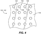
Fig. 4 is a plan view of the system ofFig. 1 or3 , showing an array of pixels. - Reference will now be made to the drawings wherein like reference numerals identify similar structural features. The systems and methods described herein can be used to reduce capacitance created by the passivation layer in photodiodes, increasing thickness of the passivation layer without increasing the mechanical stress relative to traditional photodetector configurations.
- A system includes a photodiode array (PDA) 102 one
pixel 104 of which is shown inFig. 1 . Thepixel 104 has adiffusion layer 106 within anInP cap layer 108. Thediffusion layer 106 defines afront side 110 and anillumination side 112 opposite thefront side 110. Anabsorption layer 114 is operatively connected to theillumination side 112 of the diffusion andcap layers absorption layer 114 can include InGaAs, wherein the pixel is sensitive to illumination in infrared wavelengths. Aset 116 ofoxide layers 118 alternating withnitride layers 120 are deposited on thefront side 110 of the cap anddiffusion layers - The
pixel 104 shown inFig. 1 has a PIN diode structure, which is not a part of the claimed invention, wherein thediffusion layer 106 is in contact with theabsorption layer 114 on the side of the cap anddiffusion layers set 116 of alternating oxide andnitride layers diffusion layer 106 opposite theabsorption layer 114. In the present invention thepixel 104 includes an avalanche photodiode (APD) structure as shown inFig. 3 , wherein afield control layer 122 is disposed in contact with thecap layer 108 opposite from theset 116 of alternating oxide andnitride layers grading layer 124 is disposed in contact with thefield control layer 122 opposite thecap layer 108, and wherein thegrading layer 124 is in contact with theabsorption layer 114. - With reference to
Fig. 4 , regardless of whether an APD or PIN architecture is used, thePDA 102 includes a plurality ofsimilar pixels 104 arranged in a grid pattern. Regardless of whether an APD (Fig. 3 ) or PIN (Fig. 1 ) architecture is used,contact layer 126 can be disposed in contact with theabsorption layer 114 on anillumination side 112 of theabsorption layer 114. Thecontact layer 126 can include n-doped InP. Ananti-reflective layer 128 can be deposited on thecontact layer 126 opposite theabsorption layer 114. - With reference again to
Fig. 1 (and regardless of whether the PIN architecture ofFig. 1 or the APD architecture ofFig. 3 is used), a contact metal 130 (e.g., of Indium) can be electrically connected to thediffusion layer 106 through a bump-to-stack contact layer 132 which physically separates between thecontact metal 130 and thediffusion layer 106 and set 116 ofalternating layers contact metal 130 is configured to electrically connect thediffusion layer 106 to a read-out integrated circuit (ROIC) 134 through acorresponding contact metal 136 of the ROIC, as shown inFig. 2 . Thecontact metal 130 can have an aspect ratio (height H to width W) greater than 1 to 1 wherein height H is measured from the bottom surface of thecontact metal 130 to the top surface of the contact metal 130 (as oriented inFig. 1 ), i.e. perpendicular to asurface 138 of thediffusion layer 106 where thecontact metal 130 joins the diffusion layer 106 (albeit joined by the contact layer 132), and wherein width W is measured in a direction along thesurface 138 of the diffusion layer. Thecontact metal 130 can have an aspect ratio (height to width) greater than 2 to 1, even when the ROIC 134 is connected in electrical communication with thecontact metal 130 as shown inFig. 2 . Thecontact metal 130, 136 (e.g. Indium bumps) also have flat top surface (e.g. as oriented inFig. 1 ), which favors the alignment and hybridization ofPDA 102 and ROIC 134. High press pressure can be avoided in this case, which will reduce the lateral expansion of the indium metal during press. So that the metal foot print is decreased, device capacitance will be reduced comparing with the prior art. - A method includes forming a pixel array, e.g., the photodiode array (PDA) 102 in
Fig. 4 , including a plurality ofpixels e.g pixels 104, each pixel including a diffusion layer, e.g.,diffusion layer 106, operatively connected to an absorption layer,e.g. absorption layer 114. The method includes depositing a set of alternating oxide and nitride layers, e.g.,layers Fig. 3 ). - The configurations shown herein with the alternating oxide and
nitride layers layers - The methods and systems of the present invention, as described above and shown in the drawings, provide for reduced capacitance created by the passivation layer in photodiodes, and/or increasing thickness of the passivation layer without increasing the mechanical stress relative to traditional photodetector configurations. While the apparatus and methods of the present invention have been shown and described with reference to preferred embodiments, those skilled in the art will readily appreciate that changes and/or modifications may be made thereto without departing from the scope of the invention, which is defined by the appended claims.
Claims (12)
- A system (100) comprising:a pixel (104) including a diffusion layer (106) within a cap layer (108), wherein the diffusion layer (106) defines a front side (110) and an illumination side (112) opposite the front side (110) with an absorption layer (114) operatively connected to the illumination side (112) as well as the diffusion and cap layers (106, 108); anda set of alternating oxide and nitride layers (116) deposited on the front side (110) of the cap and diffusion layers (108, 106), wherein the pixel (104) includes an avalanche photodiode (APD) structure wherein a field control layer (122) is disposed in contact with the cap layer (108) opposite from the set of alternating oxide and nitride layers (116), wherein a grading layer (124) is disposed in contact with the field control layer (122) opposite the cap layer (108), and wherein the grading layer (124) is in contact with the absorption layer (114).
- The system (100) as recited in claim 1, wherein the cap layer (108) includes InP.
- The system (100) as recited in any preceding claim, further comprising a contact layer (126) disposed in contact with the absorption layer (114) on an illumination side (112) of the absorption layer (114).
- The system (100) as recited in claim 3, wherein the contact layer (126) includes n-doped InP.
- The system (100) as recited in claim 3 or 4, further comprising an anti-reflective layer (128) deposited on the contact layer (126) opposite the absorption layer. (114)
- The system (100) as recited in any preceding claim, further comprising a contact metal (130) electrically connected to the diffusion layer (106), configured to electrically connect the diffusion layer (106) to a read-out integrated circuit, ROIC, (134).
- The system (100) as recited in claim 6, wherein the contact metal (130) has an aspect ratio, height (H) to width (W), greater than 1 to 1 with a flat top surface, wherein height (H) is measured perpendicular to a surface (138) of the diffusion layer (106) where the contact metal (130) joins the diffusion layer (106), and wherein width (W) is measured in a direction along the surface (138) of the diffusion layer (106) where the contact metal joins the diffusion layer (106).
- The system (100) as recited in claim 7, wherein the contact metal (130) has an aspect ratio, height (H) to width (W), greater than 2 to 1.
- The system (100) as recited in claim 6, 7 or 8, further comprising the ROIC (134) connected in electrical communication with the contact metal (130).
- The system (100) as recited in any preceding claim, wherein the absorption layer (114) includes InGaAs, and wherein the pixel (104) is sensitive to illumination in infrared wavelengths.
- A system (100) as recited in any preceding claim, wherein the pixel (104) is one of a plurality of similar pixels arranged in a grid pattern.
- A method comprising:forming a pixel array (102) including a plurality of pixels (104), each pixel (104) including a diffusion layer (106) within a cap layer (108) operatively connected to an absorption layer (114); anddepositing a set of alternating oxide and nitride layers (116) on a side of the diffusion layer (106) opposite the absorption layer (114), wherein the pixel (104) includes an avalanche photodiode (APD) structure wherein a field control layer (122) is disposed in contact with the cap layer (108) opposite from the set of alternating oxide and nitride layers (116), wherein a grading layer (124) is disposed in contact with the field control layer (122) opposite the cap layer (108), and wherein the grading layer (124) is in contact with the absorption layer (114).
Applications Claiming Priority (1)
| Application Number | Priority Date | Filing Date | Title |
|---|---|---|---|
| US16/814,179 US11251219B2 (en) | 2020-03-10 | 2020-03-10 | Low capacitance photo detectors |
Publications (2)
| Publication Number | Publication Date |
|---|---|
| EP3879573A1 EP3879573A1 (en) | 2021-09-15 |
| EP3879573B1 true EP3879573B1 (en) | 2022-12-21 |
Family
ID=74870714
Family Applications (1)
| Application Number | Title | Priority Date | Filing Date |
|---|---|---|---|
| EP21161779.0A Active EP3879573B1 (en) | 2020-03-10 | 2021-03-10 | Low capacitance photo detectors |
Country Status (2)
| Country | Link |
|---|---|
| US (1) | US11251219B2 (en) |
| EP (1) | EP3879573B1 (en) |
Families Citing this family (1)
| Publication number | Priority date | Publication date | Assignee | Title |
|---|---|---|---|---|
| JP7512241B2 (en) * | 2021-09-22 | 2024-07-08 | キヤノン株式会社 | Photoelectric conversion device |
Family Cites Families (19)
| Publication number | Priority date | Publication date | Assignee | Title |
|---|---|---|---|---|
| JP2002083949A (en) * | 2000-09-07 | 2002-03-22 | Nec Corp | CMOS image sensor and method of manufacturing the same |
| JP4103885B2 (en) * | 2004-11-16 | 2008-06-18 | 住友電気工業株式会社 | Zinc solid phase diffusion method for InP-based light receiving element and InP-based light receiving element |
| US7935994B2 (en) | 2005-02-24 | 2011-05-03 | Taiwan Semiconductor Manufacturing Company, Ltd. | Light shield for CMOS imager |
| US20070012948A1 (en) | 2005-07-15 | 2007-01-18 | Dries J C | Combined APD / PIN InGaAs photodetector with microlens structure and method of manufacture |
| US7598582B2 (en) * | 2007-06-13 | 2009-10-06 | The Boeing Company | Ultra low dark current pin photodetector |
| US7902540B2 (en) | 2008-05-21 | 2011-03-08 | International Business Machines Corporation | Fast P-I-N photodetector with high responsitivity |
| JP2010050417A (en) * | 2008-08-25 | 2010-03-04 | Sumitomo Electric Ind Ltd | Light-receiving element array, method of manufacturing the same, and detecting device |
| US8441032B2 (en) | 2009-06-26 | 2013-05-14 | Amplification Technologies, Inc. | Low-level signal detection by semiconductor avalanche amplification |
| SE534345C2 (en) * | 2009-09-24 | 2011-07-19 | Svedice Ab | Avalanche photodiode photodiode. |
| JPWO2012046603A1 (en) * | 2010-10-06 | 2014-02-24 | 住友電気工業株式会社 | Light receiving element, optical sensor device, and method for manufacturing light receiving element |
| KR101777225B1 (en) * | 2011-12-16 | 2017-09-12 | 한국전자통신연구원 | Avalanche photo diode and manufacturing method of the same |
| WO2013155145A1 (en) | 2012-04-10 | 2013-10-17 | Drs Rsta, Inc. | High density capacitor integrated into focal plane array processing flow |
| KR102358584B1 (en) * | 2013-05-22 | 2022-02-04 | 시-위안 왕 | Microstructure enhanced absorption photosensitive devices |
| US9647022B2 (en) | 2015-02-12 | 2017-05-09 | Taiwan Semiconductor Manufacturing Co., Ltd. | Multi-layer structure for high aspect ratio etch |
| JP6903896B2 (en) * | 2016-01-13 | 2021-07-14 | ソニーグループ株式会社 | Manufacturing method of light receiving element |
| US10032814B2 (en) | 2016-11-18 | 2018-07-24 | Taiwan Semiconductor Manufacturing Company Ltd. | Image sensor array and manufacturing method of the same |
| FR3075462B1 (en) * | 2017-12-19 | 2020-03-27 | Commissariat A L'energie Atomique Et Aux Energies Alternatives | DEVICE FOR ACQUIRING A 2D IMAGE AND A DEPTH IMAGE OF A SCENE |
| US10622324B2 (en) | 2018-02-08 | 2020-04-14 | Sensors Unlimited, Inc. | Bump structures for high density flip chip interconnection |
| US10854658B2 (en) | 2018-07-16 | 2020-12-01 | Taiwan Semiconductor Manufacturing Company, Ltd. | Image sensor with sidewall protection and method of making same |
-
2020
- 2020-03-10 US US16/814,179 patent/US11251219B2/en active Active
-
2021
- 2021-03-10 EP EP21161779.0A patent/EP3879573B1/en active Active
Also Published As
| Publication number | Publication date |
|---|---|
| US20210288100A1 (en) | 2021-09-16 |
| US11251219B2 (en) | 2022-02-15 |
| EP3879573A1 (en) | 2021-09-15 |
Similar Documents
| Publication | Publication Date | Title |
|---|---|---|
| US12113078B2 (en) | Photodetector | |
| US8026471B2 (en) | Single-photon avalanche detector-based focal plane array | |
| US20230290672A1 (en) | Image sensor with dual trench isolation structure | |
| US9773930B2 (en) | Integrated circuit with reflective material in trenches and related methods | |
| EP4230974B1 (en) | Photodetector device | |
| US10367111B2 (en) | APD focal plane arrays with backside vias | |
| EP3864707B1 (en) | Pin photodetector | |
| US8766159B2 (en) | Multicolor detectors and applications thereof | |
| US20110101483A1 (en) | Two colour photon detector | |
| US20070012948A1 (en) | Combined APD / PIN InGaAs photodetector with microlens structure and method of manufacture | |
| US11251219B2 (en) | Low capacitance photo detectors | |
| EP4131430A1 (en) | Light receiving element and electronic device | |
| US20250022978A1 (en) | Short-wave infra-red radiation detection device | |
| US10090426B2 (en) | Dark current mitigation with diffusion control | |
| US20100295141A1 (en) | Two colour photon detector | |
| US20240194714A1 (en) | Photodiode with deep trench isolation structures | |
| US9960308B2 (en) | Photoelectric conversion element | |
| US20250072149A1 (en) | Photodiode with deep trench isolation structures | |
| US20260020365A1 (en) | Photodiode with deep trench isolation structures and intermediate doped regions |
Legal Events
| Date | Code | Title | Description |
|---|---|---|---|
| PUAI | Public reference made under article 153(3) epc to a published international application that has entered the european phase |
Free format text: ORIGINAL CODE: 0009012 |
|
| STAA | Information on the status of an ep patent application or granted ep patent |
Free format text: STATUS: THE APPLICATION HAS BEEN PUBLISHED |
|
| AK | Designated contracting states |
Kind code of ref document: A1 Designated state(s): AL AT BE BG CH CY CZ DE DK EE ES FI FR GB GR HR HU IE IS IT LI LT LU LV MC MK MT NL NO PL PT RO RS SE SI SK SM TR |
|
| STAA | Information on the status of an ep patent application or granted ep patent |
Free format text: STATUS: REQUEST FOR EXAMINATION WAS MADE |
|
| 17P | Request for examination filed |
Effective date: 20220315 |
|
| RBV | Designated contracting states (corrected) |
Designated state(s): AL AT BE BG CH CY CZ DE DK EE ES FI FR GB GR HR HU IE IS IT LI LT LU LV MC MK MT NL NO PL PT RO RS SE SI SK SM TR |
|
| GRAP | Despatch of communication of intention to grant a patent |
Free format text: ORIGINAL CODE: EPIDOSNIGR1 |
|
| STAA | Information on the status of an ep patent application or granted ep patent |
Free format text: STATUS: GRANT OF PATENT IS INTENDED |
|
| INTG | Intention to grant announced |
Effective date: 20220707 |
|
| RIC1 | Information provided on ipc code assigned before grant |
Ipc: H01L 31/00 20060101ALI20220624BHEP Ipc: H01L 27/146 20060101AFI20220624BHEP |
|
| GRAS | Grant fee paid |
Free format text: ORIGINAL CODE: EPIDOSNIGR3 |
|
| GRAA | (expected) grant |
Free format text: ORIGINAL CODE: 0009210 |
|
| STAA | Information on the status of an ep patent application or granted ep patent |
Free format text: STATUS: THE PATENT HAS BEEN GRANTED |
|
| AK | Designated contracting states |
Kind code of ref document: B1 Designated state(s): AL AT BE BG CH CY CZ DE DK EE ES FI FR GB GR HR HU IE IS IT LI LT LU LV MC MK MT NL NO PL PT RO RS SE SI SK SM TR |
|
| REG | Reference to a national code |
Ref country code: GB Ref legal event code: FG4D |
|
| REG | Reference to a national code |
Ref country code: DE Ref legal event code: R096 Ref document number: 602021001011 Country of ref document: DE |
|
| REG | Reference to a national code |
Ref country code: CH Ref legal event code: EP |
|
| REG | Reference to a national code |
Ref country code: AT Ref legal event code: REF Ref document number: 1539570 Country of ref document: AT Kind code of ref document: T Effective date: 20230115 |
|
| REG | Reference to a national code |
Ref country code: IE Ref legal event code: FG4D |
|
| REG | Reference to a national code |
Ref country code: LT Ref legal event code: MG9D |
|
| REG | Reference to a national code |
Ref country code: NL Ref legal event code: MP Effective date: 20221221 |
|
| PG25 | Lapsed in a contracting state [announced via postgrant information from national office to epo] |
Ref country code: SE Free format text: LAPSE BECAUSE OF FAILURE TO SUBMIT A TRANSLATION OF THE DESCRIPTION OR TO PAY THE FEE WITHIN THE PRESCRIBED TIME-LIMIT Effective date: 20221221 Ref country code: NO Free format text: LAPSE BECAUSE OF FAILURE TO SUBMIT A TRANSLATION OF THE DESCRIPTION OR TO PAY THE FEE WITHIN THE PRESCRIBED TIME-LIMIT Effective date: 20230321 Ref country code: LT Free format text: LAPSE BECAUSE OF FAILURE TO SUBMIT A TRANSLATION OF THE DESCRIPTION OR TO PAY THE FEE WITHIN THE PRESCRIBED TIME-LIMIT Effective date: 20221221 Ref country code: FI Free format text: LAPSE BECAUSE OF FAILURE TO SUBMIT A TRANSLATION OF THE DESCRIPTION OR TO PAY THE FEE WITHIN THE PRESCRIBED TIME-LIMIT Effective date: 20221221 |
|
| REG | Reference to a national code |
Ref country code: AT Ref legal event code: MK05 Ref document number: 1539570 Country of ref document: AT Kind code of ref document: T Effective date: 20221221 |
|
| PG25 | Lapsed in a contracting state [announced via postgrant information from national office to epo] |
Ref country code: RS Free format text: LAPSE BECAUSE OF FAILURE TO SUBMIT A TRANSLATION OF THE DESCRIPTION OR TO PAY THE FEE WITHIN THE PRESCRIBED TIME-LIMIT Effective date: 20221221 Ref country code: LV Free format text: LAPSE BECAUSE OF FAILURE TO SUBMIT A TRANSLATION OF THE DESCRIPTION OR TO PAY THE FEE WITHIN THE PRESCRIBED TIME-LIMIT Effective date: 20221221 Ref country code: HR Free format text: LAPSE BECAUSE OF FAILURE TO SUBMIT A TRANSLATION OF THE DESCRIPTION OR TO PAY THE FEE WITHIN THE PRESCRIBED TIME-LIMIT Effective date: 20221221 Ref country code: GR Free format text: LAPSE BECAUSE OF FAILURE TO SUBMIT A TRANSLATION OF THE DESCRIPTION OR TO PAY THE FEE WITHIN THE PRESCRIBED TIME-LIMIT Effective date: 20230322 |
|
| PG25 | Lapsed in a contracting state [announced via postgrant information from national office to epo] |
Ref country code: NL Free format text: LAPSE BECAUSE OF FAILURE TO SUBMIT A TRANSLATION OF THE DESCRIPTION OR TO PAY THE FEE WITHIN THE PRESCRIBED TIME-LIMIT Effective date: 20221221 |
|
| PG25 | Lapsed in a contracting state [announced via postgrant information from national office to epo] |
Ref country code: SM Free format text: LAPSE BECAUSE OF FAILURE TO SUBMIT A TRANSLATION OF THE DESCRIPTION OR TO PAY THE FEE WITHIN THE PRESCRIBED TIME-LIMIT Effective date: 20221221 Ref country code: RO Free format text: LAPSE BECAUSE OF FAILURE TO SUBMIT A TRANSLATION OF THE DESCRIPTION OR TO PAY THE FEE WITHIN THE PRESCRIBED TIME-LIMIT Effective date: 20221221 Ref country code: PT Free format text: LAPSE BECAUSE OF FAILURE TO SUBMIT A TRANSLATION OF THE DESCRIPTION OR TO PAY THE FEE WITHIN THE PRESCRIBED TIME-LIMIT Effective date: 20230421 Ref country code: ES Free format text: LAPSE BECAUSE OF FAILURE TO SUBMIT A TRANSLATION OF THE DESCRIPTION OR TO PAY THE FEE WITHIN THE PRESCRIBED TIME-LIMIT Effective date: 20221221 Ref country code: EE Free format text: LAPSE BECAUSE OF FAILURE TO SUBMIT A TRANSLATION OF THE DESCRIPTION OR TO PAY THE FEE WITHIN THE PRESCRIBED TIME-LIMIT Effective date: 20221221 Ref country code: CZ Free format text: LAPSE BECAUSE OF FAILURE TO SUBMIT A TRANSLATION OF THE DESCRIPTION OR TO PAY THE FEE WITHIN THE PRESCRIBED TIME-LIMIT Effective date: 20221221 Ref country code: AT Free format text: LAPSE BECAUSE OF FAILURE TO SUBMIT A TRANSLATION OF THE DESCRIPTION OR TO PAY THE FEE WITHIN THE PRESCRIBED TIME-LIMIT Effective date: 20221221 |
|
| PG25 | Lapsed in a contracting state [announced via postgrant information from national office to epo] |
Ref country code: SK Free format text: LAPSE BECAUSE OF FAILURE TO SUBMIT A TRANSLATION OF THE DESCRIPTION OR TO PAY THE FEE WITHIN THE PRESCRIBED TIME-LIMIT Effective date: 20221221 Ref country code: PL Free format text: LAPSE BECAUSE OF FAILURE TO SUBMIT A TRANSLATION OF THE DESCRIPTION OR TO PAY THE FEE WITHIN THE PRESCRIBED TIME-LIMIT Effective date: 20221221 Ref country code: IS Free format text: LAPSE BECAUSE OF FAILURE TO SUBMIT A TRANSLATION OF THE DESCRIPTION OR TO PAY THE FEE WITHIN THE PRESCRIBED TIME-LIMIT Effective date: 20230421 Ref country code: AL Free format text: LAPSE BECAUSE OF FAILURE TO SUBMIT A TRANSLATION OF THE DESCRIPTION OR TO PAY THE FEE WITHIN THE PRESCRIBED TIME-LIMIT Effective date: 20221221 |
|
| REG | Reference to a national code |
Ref country code: DE Ref legal event code: R097 Ref document number: 602021001011 Country of ref document: DE |
|
| PLBE | No opposition filed within time limit |
Free format text: ORIGINAL CODE: 0009261 |
|
| STAA | Information on the status of an ep patent application or granted ep patent |
Free format text: STATUS: NO OPPOSITION FILED WITHIN TIME LIMIT |
|
| PG25 | Lapsed in a contracting state [announced via postgrant information from national office to epo] |
Ref country code: MC Free format text: LAPSE BECAUSE OF FAILURE TO SUBMIT A TRANSLATION OF THE DESCRIPTION OR TO PAY THE FEE WITHIN THE PRESCRIBED TIME-LIMIT Effective date: 20221221 Ref country code: DK Free format text: LAPSE BECAUSE OF FAILURE TO SUBMIT A TRANSLATION OF THE DESCRIPTION OR TO PAY THE FEE WITHIN THE PRESCRIBED TIME-LIMIT Effective date: 20221221 |
|
| 26N | No opposition filed |
Effective date: 20230922 |
|
| REG | Reference to a national code |
Ref country code: BE Ref legal event code: MM Effective date: 20230331 |
|
| PG25 | Lapsed in a contracting state [announced via postgrant information from national office to epo] |
Ref country code: LU Free format text: LAPSE BECAUSE OF NON-PAYMENT OF DUE FEES Effective date: 20230310 |
|
| REG | Reference to a national code |
Ref country code: IE Ref legal event code: MM4A |
|
| PG25 | Lapsed in a contracting state [announced via postgrant information from national office to epo] |
Ref country code: SI Free format text: LAPSE BECAUSE OF FAILURE TO SUBMIT A TRANSLATION OF THE DESCRIPTION OR TO PAY THE FEE WITHIN THE PRESCRIBED TIME-LIMIT Effective date: 20221221 Ref country code: IE Free format text: LAPSE BECAUSE OF NON-PAYMENT OF DUE FEES Effective date: 20230310 |
|
| PG25 | Lapsed in a contracting state [announced via postgrant information from national office to epo] |
Ref country code: BE Free format text: LAPSE BECAUSE OF NON-PAYMENT OF DUE FEES Effective date: 20230331 |
|
| PG25 | Lapsed in a contracting state [announced via postgrant information from national office to epo] |
Ref country code: IT Free format text: LAPSE BECAUSE OF FAILURE TO SUBMIT A TRANSLATION OF THE DESCRIPTION OR TO PAY THE FEE WITHIN THE PRESCRIBED TIME-LIMIT Effective date: 20221221 |
|
| REG | Reference to a national code |
Ref country code: CH Ref legal event code: PL |
|
| PG25 | Lapsed in a contracting state [announced via postgrant information from national office to epo] |
Ref country code: BG Free format text: LAPSE BECAUSE OF FAILURE TO SUBMIT A TRANSLATION OF THE DESCRIPTION OR TO PAY THE FEE WITHIN THE PRESCRIBED TIME-LIMIT Effective date: 20221221 |
|
| REG | Reference to a national code |
Ref country code: DE Ref legal event code: R079 Ref document number: 602021001011 Country of ref document: DE Free format text: PREVIOUS MAIN CLASS: H01L0027146000 Ipc: H10F0039180000 |
|
| PG25 | Lapsed in a contracting state [announced via postgrant information from national office to epo] |
Ref country code: BG Free format text: LAPSE BECAUSE OF FAILURE TO SUBMIT A TRANSLATION OF THE DESCRIPTION OR TO PAY THE FEE WITHIN THE PRESCRIBED TIME-LIMIT Effective date: 20221221 |
|
| PG25 | Lapsed in a contracting state [announced via postgrant information from national office to epo] |
Ref country code: CH Free format text: LAPSE BECAUSE OF NON-PAYMENT OF DUE FEES Effective date: 20240331 |
|
| PG25 | Lapsed in a contracting state [announced via postgrant information from national office to epo] |
Ref country code: CY Free format text: LAPSE BECAUSE OF FAILURE TO SUBMIT A TRANSLATION OF THE DESCRIPTION OR TO PAY THE FEE WITHIN THE PRESCRIBED TIME-LIMIT; INVALID AB INITIO Effective date: 20210310 |
|
| PG25 | Lapsed in a contracting state [announced via postgrant information from national office to epo] |
Ref country code: HU Free format text: LAPSE BECAUSE OF FAILURE TO SUBMIT A TRANSLATION OF THE DESCRIPTION OR TO PAY THE FEE WITHIN THE PRESCRIBED TIME-LIMIT; INVALID AB INITIO Effective date: 20210310 |
|
| PG25 | Lapsed in a contracting state [announced via postgrant information from national office to epo] |
Ref country code: TR Free format text: LAPSE BECAUSE OF FAILURE TO SUBMIT A TRANSLATION OF THE DESCRIPTION OR TO PAY THE FEE WITHIN THE PRESCRIBED TIME-LIMIT Effective date: 20221221 |
|
| P01 | Opt-out of the competence of the unified patent court (upc) registered |
Free format text: CASE NUMBER: UPC_APP_0018781_3879573/2025 Effective date: 20251221 |
|
| PGFP | Annual fee paid to national office [announced via postgrant information from national office to epo] |
Ref country code: GB Payment date: 20260219 Year of fee payment: 6 |
|
| PGFP | Annual fee paid to national office [announced via postgrant information from national office to epo] |
Ref country code: DE Payment date: 20260219 Year of fee payment: 6 |
|
| PGFP | Annual fee paid to national office [announced via postgrant information from national office to epo] |
Ref country code: FR Payment date: 20260219 Year of fee payment: 6 |
|
| PG25 | Lapsed in a contracting state [announced via postgrant information from national office to epo] |
Ref country code: CH Free format text: THE PATENT HAS BEEN ANNULLED BY A DECISION OF A NATIONAL AUTHORITY Effective date: 20240331 |
|
| PG25 | Lapsed in a contracting state [announced via postgrant information from national office to epo] |
Ref country code: MT Free format text: LAPSE BECAUSE OF NON-PAYMENT OF DUE FEES Effective date: 20230310 |