EP3879285A1 - Insulation detection circuit of vehicle-mounted bidirectional charger and detection method therefor - Google Patents
Insulation detection circuit of vehicle-mounted bidirectional charger and detection method therefor Download PDFInfo
- Publication number
- EP3879285A1 EP3879285A1 EP18939932.2A EP18939932A EP3879285A1 EP 3879285 A1 EP3879285 A1 EP 3879285A1 EP 18939932 A EP18939932 A EP 18939932A EP 3879285 A1 EP3879285 A1 EP 3879285A1
- Authority
- EP
- European Patent Office
- Prior art keywords
- circuit
- resistor
- output
- voltage
- sampling
- Prior art date
- Legal status (The legal status is an assumption and is not a legal conclusion. Google has not performed a legal analysis and makes no representation as to the accuracy of the status listed.)
- Granted
Links
Images



Classifications
-
- G—PHYSICS
- G01—MEASURING; TESTING
- G01R—MEASURING ELECTRIC VARIABLES; MEASURING MAGNETIC VARIABLES
- G01R31/00—Arrangements for testing electric properties; Arrangements for locating electric faults; Arrangements for electrical testing characterised by what is being tested not provided for elsewhere
- G01R31/005—Testing of electric installations on transport means
- G01R31/006—Testing of electric installations on transport means on road vehicles, e.g. automobiles or trucks
- G01R31/007—Testing of electric installations on transport means on road vehicles, e.g. automobiles or trucks using microprocessors or computers
-
- G—PHYSICS
- G01—MEASURING; TESTING
- G01R—MEASURING ELECTRIC VARIABLES; MEASURING MAGNETIC VARIABLES
- G01R27/00—Arrangements for measuring resistance, reactance, impedance, or electric characteristics derived therefrom
- G01R27/02—Measuring real or complex resistance, reactance, impedance, or other two-pole characteristics derived therefrom, e.g. time constant
- G01R27/025—Measuring very high resistances, e.g. isolation resistances, i.e. megohm-meters
-
- G—PHYSICS
- G01—MEASURING; TESTING
- G01R—MEASURING ELECTRIC VARIABLES; MEASURING MAGNETIC VARIABLES
- G01R31/00—Arrangements for testing electric properties; Arrangements for locating electric faults; Arrangements for electrical testing characterised by what is being tested not provided for elsewhere
- G01R31/12—Testing dielectric strength or breakdown voltage ; Testing or monitoring effectiveness or level of insulation, e.g. of a cable or of an apparatus, for example using partial discharge measurements; Electrostatic testing
- G01R31/14—Circuits therefor, e.g. for generating test voltages, sensing circuits
-
- G—PHYSICS
- G01—MEASURING; TESTING
- G01R—MEASURING ELECTRIC VARIABLES; MEASURING MAGNETIC VARIABLES
- G01R31/00—Arrangements for testing electric properties; Arrangements for locating electric faults; Arrangements for electrical testing characterised by what is being tested not provided for elsewhere
- G01R31/40—Testing power supplies
- G01R31/42—AC power supplies
Definitions
- the present invention relates to charging equipment, and more particularly, to an insulation detection circuit and a detection method thereof for a two-way on-board charger.
- An on-board charger is a very important component in an electric vehicle.
- the quality of the on-board charger directly affects the safety and reliability of the vehicle.
- the insulation quality between a live line and a ground line of the on-board charger is in turn related to the performances of the whole vehicle. For example, the failure of the insulation between the live line and the ground line can easily cause damage to components and even electric shock.
- the previous detection means is to use instruments to detect after a power failure, which is not only tedious to operate, but also cannot be monitored in real time.
- the present invention provides an insulation detection circuit and a detection method thereof for a two-way on-board charger, which are used for detecting whether there is an insulation failure between an AC output and a vehicle body when the on-board charger operates in a pure inverting mode.
- the technical solution adopted by the present invention is to design an insulation detection circuit for a two-way on-board charger, the insulation detection circuit comprising an inverter circuit, a first Y capacitor connected between an output live line and a ground line of the inverter circuit, and a second Y capacitor connected between an output neutral line and the ground line of the inverter circuit, and further comprising a live line sampling circuit and a neutral line sampling circuit correspondingly connected with the output live line and the output neutral line of the inverter circuit, and a controller connected with the live line sampling circuit and the neutral line sampling circuit, wherein the controller determines an insulation state of the two-way on-board charger according to two sampling voltages.
- a summing circuit is provided among the controller, the live line sampling circuit and the neutral line sampling circuit and configured to perform summing processing on the two sampling voltages and output the summed voltage, and the summed voltage is transmitted to the controller; and the controller determines an insulation state of the two-way on-board charger according to the summed voltage.
- the live line sampling circuit and the neutral line sampling circuit have the same circuit structure, and each comprises a voltage dividing circuit, a bias power source, a negative bias circuit, and an impedance matching circuit, wherein the voltage dividing circuit is connected with the output live line or the output neutral line, and configured to proportionally reduce voltages to output a divided voltage; the negative bias circuit is connected between an output terminal of the voltage dividing circuit and the bias power source and configured to bias the divided voltage; and the impedance matching circuit is connected with the output terminal of the voltage dividing circuit, and configured to perform impedance matching and output a sampling voltage.
- the voltage dividing circuit in the live line sampling circuit comprises a first resistor and a sixth resistor which are connected in series between the output live line and the ground line, and a connection end of the first resistor and the sixth resistor serves as the output terminal of the voltage dividing circuit;
- the voltage dividing circuit in the neutral line sampling circuit comprises a second resistor and a fifth resistor which are connected in series between the output neutral line and the ground line, and a connection end of the second resistor and the fifth resistor serves as the output terminal of the voltage dividing circuit.
- the negative bias circuit in the live line sampling circuit comprises a fourth resistor, one end of the fourth resistor being connected with the bias power source, and the other end of the fourth resistor being connected with the connection end of the first resistor and the sixth resistor; and the negative bias circuit in the neutral line sampling circuit comprises a third resistor, one end of the third resistor being connected with the bias power source, and the other end of the third resistor being connected with the connection end of the second resistor and the fifth resistor.
- the impedance matching circuit uses an emitter follower or a voltage follower.
- the impedance matching circuit in the live line sampling circuit comprises a first operational amplifier, wherein a non-inverting input terminal of the first operational amplifier is connected with the connection end of the first resistor and the sixth resistor, and an output terminal of the first operational amplifier is connected with its inverting input terminal and outputs the sampling voltage;
- the impedance matching circuit in the neutral line sampling circuit comprises a second operational amplifier, wherein a non-inverting input terminal of the second operational amplifier is connected with the connection end of the second resistor and the fifth resistor, and an output terminal of the second operational amplifier is connected with its inverting input terminal and outputs the sampling voltage.
- the summing circuit comprises a seventh resistor, an eighth resistor, a ninth resistor, and an output terminal A; the seventh resistor is connected in series between the output terminal A and an output terminal of the first operational amplifier; an eighth resistor is connected in series between the output terminal A and an output terminal of the second operational amplifier; the ninth resistor is connected in series between the output terminal A and the ground line; and the output terminal A outputs the summed voltage.
- the present invention further discloses a detection method for an insulation detection circuit for a two-way on-board charger, the detection method comprising the following steps: sampling voltages on an output live line and an output neutral line of the inverter circuit respectively to obtain a sampling voltage; and determining an insulation state of the two-way on-board charger according to two sampling voltages.
- the detection method specifically comprises the following steps: reducing the voltages on the output live line and on the output neutral line of the inverter circuit proportionally by using a voltage dividing circuit respectively to generate a divided voltage; performing bias processing on the divided voltage by using the negative bias circuit, performing impedance matching on the divided voltage subjected to bias processing, and outputting a sampling voltage; performing summing processing on the sampling voltage of the output live line and the sampling voltage of the output neutral line by using a summing circuit, and outputting the summed voltage; and determining an insulation state of the two-way on-board charger according to the summed voltage.
- the present invention when the on-board charger operates in an inverting mode, the insulation impedance of the output live line L and the output neutral line N to the ground is detected, and whether there is insulation failure between the AC output in the pure inversion mode and the vehicle body is determined, thereby eliminating the hidden danger of electric shock to personnel. Meanwhile, the present invention has the advantages of simple and practical structure, easy implementation and low cost.
- the on-board charger When the on-board charger operates in an inverting state, due to the requirements of a forward on-board charger (OBC) on the electromagnetic interference (EMI), there is a Y capacitor on each of the output line line L and the output neutral line N on an AC output port to the ground line during the inversion, and Y capacitance values of the output live line and the output neutral line to the ground are equal.
- the output live line L and the output neutral line N generate a voltage to the ground, respectively, and the phases of the two voltages are staggered by 180 degrees.
- the amplitudes of the voltages are related to a ratio of the capacitance values of the output live line L and the output neutral line N of the capacitor.
- the present invention discloses an insulation detection circuit and a detection method thereof for a two-way on-board charger. According to this method, in an inversion mode, the insulation impedances of the output live line L and the output neutral line N to the ground are obtained by detecting the voltages of the output live line L and the output neutral line N to the ground. Whether there is an insulation failure between AC output and the vehicle body when the on-board charger operates in a pure inversion mode is detected by using the insulation impedance, thereby eliminating the hidden danger of electric shock to personnel.
- the insulation detection circuit for the two-way on-board charger disclosed by the present invention comprises an inverter circuit, a first Y capacitor C1 connected between an output live line and a ground line of the inverter circuit, a second Y capacitor C2 connected between an output neutral line and the ground line of the inverter circuit, a live line sampling circuit and a neutral line sampling circuit which are correspondingly connected with the output live line and the output neutral line of the inverter circuit, and a controller connected with the live line sampling circuit and the neutral line sampling circuit.
- the live line sampling circuit and the neutral line sampling circuit output a sampling voltage, respectively.
- the controller determines an insulation state of the two-way on-board charger according to the two sampling voltages.
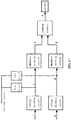
- FIG. 1 is a a principle block diagram of a preferred embodiment.
- a summing circuit is provided among the controller, the live line sampling circuit and the neutral line sampling circuit.
- the summing circuit is configured to perform summing processing on the two sampling voltages to obtain the summed voltage, and transmit the summed voltage to the controller.
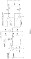
- the controller determines an insulation state of the two-way on-board charger according to the summed voltage. It should be noted that the summing processing can be calculated inside the controller, and a circuit diagram of its embodiment is shown in FIG. 2 .
- the summing processing may also be performed outside the controller. After the processing is completed, the summed voltage is transmitted to the controller, and a circuit diagram of its embodiment is shown in FIG. 3 .
- the live line sampling circuit and the neutral line sampling circuit have the same circuit structure, and each comprises a voltage dividing circuit, a bias power source, a negative bias circuit, and an impedance matching circuit.
- the voltage dividing circuit is connected with the output live line or the output neutral line, and configured to proportionally reduce voltages and output a divided voltage;
- the negative bias circuit is connected between an output terminal of the voltage dividing circuit and the bias power source and configured to bias the divided voltage.
- the impedance matching circuit is connected with the output terminal of the voltage dividing circuit, and configured to perform impedance matching and output a sampling voltage. It should be noted that the impedance matching circuit can match the impedances of an input terminal and an output terminal, so that the input impedance is high and the output impedance is low, thereby enhancing the load capacity.
- the voltage dividing circuit in the live line sampling circuit comprises a first resistor R1 and a sixth resistor R6 which are connected in series between the output live line and the ground line, and a connecting end G of the first resistor and the sixth resistor serves as the output terminal of the voltage dividing circuit.
- the voltage dividing circuit in the neutral line sampling circuit comprises a second resistor R2 and a fifth resistor R5 which are connected in series between the output neutral line and the ground line, and a connection end B of the second resistor and the fifth resistor serves as the output terminal of the voltage dividing circuit.
- the negative bias circuit in the live line sampling circuit comprises a fourth resistor R4, wherein one end of the fourth resistor is connected with the bias power source, and the other end of the fourth resistor is connected with the connection end C of the first resistor and the sixth resistor.
- the negative bias circuit in the neutral line sampling circuit comprises a third resistor R3, wherein one end of the third resistor is connected with the bias power source, and the other end of the third resistor is connected with the connection end B of the second resistor and the fifth resistor.
- R3 R4.
- the impedance matching circuit uses an emitter follower or a voltage follower.
- the impedance matching circuit in the live line sampling circuit comprises a first operational amplifier oab1.
- a non-inverting input terminal of the first operational amplifier is connected with the connection end C of the first resistor and the sixth resistor.
- An output terminal of the first operational amplifier is connected with its inverting input terminal and outputs the sampling voltage.
- the impedance matching circuit in the neutral line sampling circuit comprises a second operational amplifier oab2.
- a non-inverting input terminal of the second operational amplifier is connected with the connection end B of the second resistor and the fifth resistor.
- An output terminal of the second operational amplifier is connected with its inverting input terminal and outputs the sampling voltage.
- the summing circuit comprises a seventh resistor R7, an eighth resistor R8, a ninth resistor R9, and an output terminal A.
- the seventh resistor R7 is connected in series between the output terminal A and the output terminal of the first operational amplifier.
- the eighth resistor R8 is connected in series between the output terminal A and the output terminal of the second operational amplifier.
- the ninth resistor R9 is connected in series between the output terminal A and the ground line. The output terminal A outputs the summed voltage to the controller.
- the Y capacitors causes the output live line L and the output neutral line N to generate voltages VL and VN to the ground, respectively.
- phases of these two voltages differ by 180 degrees.
- VL Vac ⁇ 2 ⁇ sin 2 ⁇ ⁇ ⁇ f ⁇ t + ⁇ ⁇ C 1 C 1 + C 2
- VN Vac ⁇ 2 ⁇ sin 2 ⁇ ⁇ ⁇ f ⁇ t ⁇ C 2 C 1 + C 2
- f is the frequency of an AC voltage
- t is a time
- the resistors R2 and R5 are connected between the output neutral line N and the ground line. The voltage on the output neutral line N is proportionally reduced.
- a voltage VB1 is formed at a point B of the connection end of R2 and R5.
- a resistor R3 is added between the bias power source v_pwl1 and the point B, and v_pwl1 and R3 and R5 form a DC bias voltage VB2 to a point C.
- the voltage VB at the point B is a sum of VB1 and VB2.
- the resistors R1 and R6 are connected between the output live line L and the ground line. The voltage on the output live line L is proportionally reduced.
- a voltage VC1 is formed at the point C of the connection end of R1 and R6.
- a resistor R4 is added between the bias power source v_pwl1 and the point C, and v_pwl1 and R5 and R6 form a DC bias voltage VC2 to the point C.
- the voltage VC at the point C is a sum of VC1 and VC2.
- the voltage VD at a point D of an output terminal D of the first operational amplifier is equal to VC.
- the voltage VE at a point E of an output terminal E of the second operational amplifier is equal to VB.
- the voltages at the points D and E are added to the point A via the resistors R7 and R8.
- VA Vac ⁇ 2 ⁇ sin 2 ⁇ ⁇ f ⁇ t ⁇ ⁇ C 1 C 1 + C 2 ⁇ R 5 ⁇ R 1 + R 6 + C 2 C 1 + C 2 ⁇ R 6 ⁇ R 2 + R 5 R 2 + R 5 ⁇ R 1 + R 6 + V _ PWL 1 ⁇ R 6 R 4 + R 6 + V _ PWL 1 ⁇ R 5 R 3 + R 5
- the voltage at the point A in Fig.2 and FIG. 3 is sent to an AD sampling port of the controller MCU.
- the impedances of the output live line L and the output neutral line N to the ground are infinite, that is, pwlr1 is infinite in FIG. 3 .
- the value of the Y capacitor C1 of the output live line L to the ground is equal to the value of the Y capacitor C2 of the output neutral line N to the ground.
- a divided voltage VB1 of the output live line L to the ground line and a divided voltage VC1 of the output neutral line N to the ground line add up to zero, which is as shown in the following formula;
- VB 1 + VC 1 Vac ⁇ 2 ⁇ sin 2 ⁇ ⁇ f ⁇ t ⁇ ⁇ C 1 C 1 + C 2 ⁇ R 5 ⁇ R 1 + R 6 + C 2 C 1 + C 2 ⁇ R 6 ⁇ R 2 + R 5 R 2 + R 5 ⁇ R 1 + R 6
- the controller MCU reads a voltage value at the point A through AD sampling.
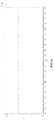
- the voltage value at the point A is equal to a sum of negative bias voltage values of the output live line L and the output neutral line N (the voltage at the point A is shown in FIG. 4 ).
- the summed voltage remains constant in amplitude, and the graph shows a straight line.
- the controller MCU determines whether the output live line L and the output neutral line N are normally insulated. In the normal state, the insulation resistance pwlr1 is considered to be infinite, and the insulation resistance pwlr1 is ignored in the above formula.
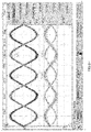
- FIG. 6 shows voltage waveforms at various points when the insulation is normal.
- VL is a voltage of the output live line L to the ground
- VN is a voltage of the output neutral line N to the ground
- VA0 is a voltage at an output terminal of R7
- VA1 is a voltage at an output terminal of R8.
- the impedance of the output live line L or the output neutral line N to the ground line is decreasing. That is, PWLr1 in FIG. 2 or FIG. 3 decreases from infinity, and the impedance of the output live line L to the ground will decrease. In this case, the voltage of VL to the ground line and the voltage of VN to the ground line will lose balance, and the sum of VN and VL is no longer equal to zero. According to the actual measurement shown in FIG. 5 , the amplitude of the summed voltage shows a sine wave waveform. The controller MCU will determine that the insulation fails according to the voltage value obtained by AD sampling, and meanwhile determine the amplitude of the value of the insulation resistance.
- FIG. 7 shows voltage waveforms at various points when the insulation fails.
- VL is a voltage of the output live line L to the ground
- VN is a voltage of the output neutral line N to the ground
- VA0 is a voltage at the output terminal of R7
- VA1 is a voltage at the output terminal of R8.
- the controller MCU uses two different AD sampling ports to input samplings of VL and VN to the MCU, and performs summing processing.
- the present invention further discloses a detection method for an insulation detection circuit for a two-way on-board charger.
- the detection circuit comprises an inverter circuit, a first Y capacitor C1 connected between an output live line and a ground line of the inverter circuit, and a second Y capacitor C2 connected between an output neutral line and the ground line of the inverter circuit.
- the detection method comprises the following steps: sampling voltages on the output live line and the output neutral line of the inverter circuit, respectively; and determining an insulation state of the two-way on-board charger according to the two sampling voltages.
- the detection method comprises the following steps: reducing voltages on the output live line and on the output neutral line of the inverter circuit proportionally by using a voltage dividing circuit respectively to generate a divided voltage; performing bias processing on the divided voltage by using a negative bias circuit, performing impedance matching on the divided voltage subjected to bias processing, and outputting a sampling voltage; performing summing processing on the sampling voltage of the output live line and the sampling voltage of the output neutral line by using a summing circuit to obtain a summed voltage; and determining an insulation state of the two-way on-board charger according to the summed voltage.
Landscapes
- Physics & Mathematics (AREA)
- General Physics & Mathematics (AREA)
- Engineering & Computer Science (AREA)
- Computer Hardware Design (AREA)
- Microelectronics & Electronic Packaging (AREA)
- Chemical & Material Sciences (AREA)
- Combustion & Propulsion (AREA)
- Power Engineering (AREA)
- Testing Of Short-Circuits, Discontinuities, Leakage, Or Incorrect Line Connections (AREA)
- Electric Propulsion And Braking For Vehicles (AREA)
- Charge And Discharge Circuits For Batteries Or The Like (AREA)
Abstract
Description
- The present invention relates to charging equipment, and more particularly, to an insulation detection circuit and a detection method thereof for a two-way on-board charger.
- The energy crisis and environmental pollution have become increasingly serious worldwide, so the entire traditional automobile industry and the world's objective environment are facing severe challenges. With the strengthening of public environmental awareness, advocating green travel and changing the travel structure have become mainstream. With the plans of governments in developed countries to develop new energy vehicles, the Chinese government has also announced corresponding new energy vehicle development plans, and new energy vehicles have also been included in seven major emerging strategic industries. The new energy vehicles are currently the most mainstream of electric vehicles. An on-board charger is a very important component in an electric vehicle. The quality of the on-board charger directly affects the safety and reliability of the vehicle. The insulation quality between a live line and a ground line of the on-board charger is in turn related to the performances of the whole vehicle. For example, the failure of the insulation between the live line and the ground line can easily cause damage to components and even electric shock. The previous detection means is to use instruments to detect after a power failure, which is not only tedious to operate, but also cannot be monitored in real time.
- Therefore, there is an urgent need in the industry to develop an insulation detection circuit and a detection method thereof that are simple to operate and can detect insulation in real time in an inverting mode.
- In order to solve the problems existing in the prior art, the present invention provides an insulation detection circuit and a detection method thereof for a two-way on-board charger, which are used for detecting whether there is an insulation failure between an AC output and a vehicle body when the on-board charger operates in a pure inverting mode.
- The technical solution adopted by the present invention is to design an insulation detection circuit for a two-way on-board charger, the insulation detection circuit comprising an inverter circuit, a first Y capacitor connected between an output live line and a ground line of the inverter circuit, and a second Y capacitor connected between an output neutral line and the ground line of the inverter circuit, and further comprising a live line sampling circuit and a neutral line sampling circuit correspondingly connected with the output live line and the output neutral line of the inverter circuit, and a controller connected with the live line sampling circuit and the neutral line sampling circuit, wherein the controller determines an insulation state of the two-way on-board charger according to two sampling voltages.
- A summing circuit is provided among the controller, the live line sampling circuit and the neutral line sampling circuit and configured to perform summing processing on the two sampling voltages and output the summed voltage, and the summed voltage is transmitted to the controller; and the controller determines an insulation state of the two-way on-board charger according to the summed voltage.
- The live line sampling circuit and the neutral line sampling circuit have the same circuit structure, and each comprises a voltage dividing circuit, a bias power source, a negative bias circuit, and an impedance matching circuit, wherein the voltage dividing circuit is connected with the output live line or the output neutral line, and configured to proportionally reduce voltages to output a divided voltage; the negative bias circuit is connected between an output terminal of the voltage dividing circuit and the bias power source and configured to bias the divided voltage; and the impedance matching circuit is connected with the output terminal of the voltage dividing circuit, and configured to perform impedance matching and output a sampling voltage.
- The voltage dividing circuit in the live line sampling circuit comprises a first resistor and a sixth resistor which are connected in series between the output live line and the ground line, and a connection end of the first resistor and the sixth resistor serves as the output terminal of the voltage dividing circuit; the voltage dividing circuit in the neutral line sampling circuit comprises a second resistor and a fifth resistor which are connected in series between the output neutral line and the ground line, and a connection end of the second resistor and the fifth resistor serves as the output terminal of the voltage dividing circuit.
- The negative bias circuit in the live line sampling circuit comprises a fourth resistor, one end of the fourth resistor being connected with the bias power source, and the other end of the fourth resistor being connected with the connection end of the first resistor and the sixth resistor; and the negative bias circuit in the neutral line sampling circuit comprises a third resistor, one end of the third resistor being connected with the bias power source, and the other end of the third resistor being connected with the connection end of the second resistor and the fifth resistor.
- The impedance matching circuit uses an emitter follower or a voltage follower.
- The impedance matching circuit in the live line sampling circuit comprises a first operational amplifier, wherein a non-inverting input terminal of the first operational amplifier is connected with the connection end of the first resistor and the sixth resistor, and an output terminal of the first operational amplifier is connected with its inverting input terminal and outputs the sampling voltage; the impedance matching circuit in the neutral line sampling circuit comprises a second operational amplifier, wherein a non-inverting input terminal of the second operational amplifier is connected with the connection end of the second resistor and the fifth resistor, and an output terminal of the second operational amplifier is connected with its inverting input terminal and outputs the sampling voltage.
- The summing circuit comprises a seventh resistor, an eighth resistor, a ninth resistor, and an output terminal A; the seventh resistor is connected in series between the output terminal A and an output terminal of the first operational amplifier; an eighth resistor is connected in series between the output terminal A and an output terminal of the second operational amplifier; the ninth resistor is connected in series between the output terminal A and the ground line; and the output terminal A outputs the summed voltage.
- The present invention further discloses a detection method for an insulation detection circuit for a two-way on-board charger, the detection method comprising the following steps: sampling voltages on an output live line and an output neutral line of the inverter circuit respectively to obtain a sampling voltage; and determining an insulation state of the two-way on-board charger according to two sampling voltages.
- In an embodiment, the detection method specifically comprises the following steps: reducing the voltages on the output live line and on the output neutral line of the inverter circuit proportionally by using a voltage dividing circuit respectively to generate a divided voltage; performing bias processing on the divided voltage by using the negative bias circuit, performing impedance matching on the divided voltage subjected to bias processing, and outputting a sampling voltage; performing summing processing on the sampling voltage of the output live line and the sampling voltage of the output neutral line by using a summing circuit, and outputting the summed voltage; and determining an insulation state of the two-way on-board charger according to the summed voltage.
- According to the present invention, when the on-board charger operates in an inverting mode, the insulation impedance of the output live line L and the output neutral line N to the ground is detected, and whether there is insulation failure between the AC output in the pure inversion mode and the vehicle body is determined, thereby eliminating the hidden danger of electric shock to personnel. Meanwhile, the present invention has the advantages of simple and practical structure, easy implementation and low cost.
-
-
FIG. 1 is a a principle block diagram of a preferred embodiment of the present invention; -
FIG. 2 is a circuit diagram without a summing circuit; -
FIG. 3 is a circuit diagram with a summing circuit; -
FIG. 4 is a waveform diagram of a summed voltage when the insulation is normal; -
FIG. 5 is a waveform diagram of a summed voltage when the insulation fails; -
FIG. 6 is a waveform diagram of a voltage at each point when the insulation is normal; and -
FIG. 7 is a waveform diagram of a voltage at each point when the insulation fails. - In order to make the objectives, technical solutions, and advantages of the present invention clearer, the present invention is further described in detail below with reference to the accompanying drawings and embodiments. It should be understood that the specific embodiments described herein are only used to explain the present invention and are not used to limit the present invention.
- When the on-board charger operates in an inverting state, due to the requirements of a forward on-board charger (OBC) on the electromagnetic interference (EMI), there is a Y capacitor on each of the output line line L and the output neutral line N on an AC output port to the ground line during the inversion, and Y capacitance values of the output live line and the output neutral line to the ground are equal. In the presence of the Y capacitors, the output live line L and the output neutral line N generate a voltage to the ground, respectively, and the phases of the two voltages are staggered by 180 degrees. The amplitudes of the voltages are related to a ratio of the capacitance values of the output live line L and the output neutral line N of the capacitor. When the insulation of the output live line L or the output neutral line N to the ground fails, the voltage of the output live line L or the output neutral line N to the ground will lose balance.
- The present invention discloses an insulation detection circuit and a detection method thereof for a two-way on-board charger. According to this method, in an inversion mode, the insulation impedances of the output live line L and the output neutral line N to the ground are obtained by detecting the voltages of the output live line L and the output neutral line N to the ground. Whether there is an insulation failure between AC output and the vehicle body when the on-board charger operates in a pure inversion mode is detected by using the insulation impedance, thereby eliminating the hidden danger of electric shock to personnel.
- The insulation detection circuit for the two-way on-board charger disclosed by the present invention comprises an inverter circuit, a first Y capacitor C1 connected between an output live line and a ground line of the inverter circuit, a second Y capacitor C2 connected between an output neutral line and the ground line of the inverter circuit, a live line sampling circuit and a neutral line sampling circuit which are correspondingly connected with the output live line and the output neutral line of the inverter circuit, and a controller connected with the live line sampling circuit and the neutral line sampling circuit. The live line sampling circuit and the neutral line sampling circuit output a sampling voltage, respectively. The controller determines an insulation state of the two-way on-board charger according to the two sampling voltages.
-
FIG. 1 is a a principle block diagram of a preferred embodiment. A summing circuit is provided among the controller, the live line sampling circuit and the neutral line sampling circuit. The summing circuit is configured to perform summing processing on the two sampling voltages to obtain the summed voltage, and transmit the summed voltage to the controller. The controller determines an insulation state of the two-way on-board charger according to the summed voltage. It should be noted that the summing processing can be calculated inside the controller, and a circuit diagram of its embodiment is shown inFIG. 2 . The summing processing may also be performed outside the controller. After the processing is completed, the summed voltage is transmitted to the controller, and a circuit diagram of its embodiment is shown inFIG. 3 . - In the above embodiments, the live line sampling circuit and the neutral line sampling circuit have the same circuit structure, and each comprises a voltage dividing circuit, a bias power source, a negative bias circuit, and an impedance matching circuit. The voltage dividing circuit is connected with the output live line or the output neutral line, and configured to proportionally reduce voltages and output a divided voltage; The negative bias circuit is connected between an output terminal of the voltage dividing circuit and the bias power source and configured to bias the divided voltage. The impedance matching circuit is connected with the output terminal of the voltage dividing circuit, and configured to perform impedance matching and output a sampling voltage. It should be noted that the impedance matching circuit can match the impedances of an input terminal and an output terminal, so that the input impedance is high and the output impedance is low, thereby enhancing the load capacity.
- Referring to the embodiments shown in
FIG. 2 andFIG. 3 , the voltage dividing circuit in the live line sampling circuit comprises a first resistor R1 and a sixth resistor R6 which are connected in series between the output live line and the ground line, and a connecting end G of the first resistor and the sixth resistor serves as the output terminal of the voltage dividing circuit. The voltage dividing circuit in the neutral line sampling circuit comprises a second resistor R2 and a fifth resistor R5 which are connected in series between the output neutral line and the ground line, and a connection end B of the second resistor and the fifth resistor serves as the output terminal of the voltage dividing circuit. A voltage division ratio is determined by a ratio of values of the first resistor R1 to the sixth resistor R6, and a ratio of values of the second resistor R2 to the fifth resistor R5. In this embodiment, R1=R2, R5=R6. - The negative bias circuit in the live line sampling circuit comprises a fourth resistor R4, wherein one end of the fourth resistor is connected with the bias power source, and the other end of the fourth resistor is connected with the connection end C of the first resistor and the sixth resistor. The negative bias circuit in the neutral line sampling circuit comprises a third resistor R3, wherein one end of the third resistor is connected with the bias power source, and the other end of the third resistor is connected with the connection end B of the second resistor and the fifth resistor. In this embodiment, R3=R4.
- In this embodiment, the impedance matching circuit uses an emitter follower or a voltage follower.
- The impedance matching circuit in the live line sampling circuit comprises a first operational amplifier oab1. A non-inverting input terminal of the first operational amplifier is connected with the connection end C of the first resistor and the sixth resistor. An output terminal of the first operational amplifier is connected with its inverting input terminal and outputs the sampling voltage. The impedance matching circuit in the neutral line sampling circuit comprises a second operational amplifier oab2. A non-inverting input terminal of the second operational amplifier is connected with the connection end B of the second resistor and the fifth resistor. An output terminal of the second operational amplifier is connected with its inverting input terminal and outputs the sampling voltage.
- In this embodiment as shown in
FIG. 3 , the summing circuit comprises a seventh resistor R7, an eighth resistor R8, a ninth resistor R9, and an output terminal A. The seventh resistor R7 is connected in series between the output terminal A and the output terminal of the first operational amplifier. The eighth resistor R8 is connected in series between the output terminal A and the output terminal of the second operational amplifier. The ninth resistor R9 is connected in series between the output terminal A and the ground line. The output terminal A outputs the summed voltage to the controller. - The working principle of the present invention is described in detail below with reference to
FIG. 3 . There are Y capacitors for the output live line L and the output neutral line N of the converter circuit of the charger, that is, the first Y capacitor C1 and the second Y capacitor C2, where C1=C2. The Y capacitors causes the output live line L and the output neutral line N to generate voltages VL and VN to the ground, respectively. In addition, phases of these two voltages differ by 180 degrees. The amplitudes of these two voltages are related to the ratio of the Y capacitors, in which:

- In the formulas, f is the frequency of an AC voltage, and t is a time.
- The resistors R2 and R5 are connected between the output neutral line N and the ground line. The voltage on the output neutral line N is proportionally reduced. A voltage VB1 is formed at a point B of the connection end of R2 and R5. A resistor R3 is added between the bias power source v_pwl1 and the point B, and v_pwl1 and R3 and R5 form a DC bias voltage VB2 to a point C. The voltage VB at the point B is a sum of VB1 and VB2.
- In which,


- The resistors R1 and R6 are connected between the output live line L and the ground line. The voltage on the output live line L is proportionally reduced. A voltage VC1 is formed at the point C of the connection end of R1 and R6. A resistor R4 is added between the bias power source v_pwl1 and the point C, and v_pwl1 and R5 and R6 form a DC bias voltage VC2 to the point C. The voltage VC at the point C is a sum of VC1 and VC2.


- After the voltage at the point C passes through the impedance matching circuit, the voltage VD at a point D of an output terminal D of the first operational amplifier is equal to VC. In the same way, after the voltage at the point B passes through the impedance matching circuit, the voltage VE at a point E of an output terminal E of the second operational amplifier is equal to VB. The voltages at the points D and E are added to the point A via the resistors R7 and R8. The voltage at the point A is:

Formulas 1 to 9.
- The voltage at the point A in
Fig.2 andFIG. 3 is sent to an AD sampling port of the controller MCU. In a normal state, the impedances of the output live line L and the output neutral line N to the ground are infinite, that is, pwlr1 is infinite inFIG. 3 . In addition, the value of the Y capacitor C1 of the output live line L to the ground is equal to the value of the Y capacitor C2 of the output neutral line N to the ground. In a normal insulation state, a divided voltage VB1 of the output live line L to the ground line and a divided voltage VC1 of the output neutral line N to the ground line add up to zero, which is as shown in the following formula;

- The controller MCU reads a voltage value at the point A through AD sampling. The voltage value at the point A is equal to a sum of negative bias voltage values of the output live line L and the output neutral line N (the voltage at the point A is shown in
FIG. 4 ). The summed voltage remains constant in amplitude, and the graph shows a straight line. In this case, the controller MCU determines whether the output live line L and the output neutral line N are normally insulated. In the normal state, the insulation resistance pwlr1 is considered to be infinite, and the insulation resistance pwlr1 is ignored in the above formula.FIG. 6 shows voltage waveforms at various points when the insulation is normal. VL is a voltage of the output live line L to the ground, VN is a voltage of the output neutral line N to the ground, VA0 is a voltage at an output terminal of R7, and VA1 is a voltage at an output terminal of R8. - When the output live line L or the output neutral line N has an insulation failure to the ground line, the impedance of the output live line L or the output neutral line N to the ground line is decreasing. That is, PWLr1 in
FIG. 2 orFIG. 3 decreases from infinity, and the impedance of the output live line L to the ground will decrease. In this case, the voltage of VL to the ground line and the voltage of VN to the ground line will lose balance, and the sum of VN and VL is no longer equal to zero. According to the actual measurement shown inFIG. 5 , the amplitude of the summed voltage shows a sine wave waveform. The controller MCU will determine that the insulation fails according to the voltage value obtained by AD sampling, and meanwhile determine the amplitude of the value of the insulation resistance.FIG. 7 shows voltage waveforms at various points when the insulation fails. VL is a voltage of the output live line L to the ground, VN is a voltage of the output neutral line N to the ground, VA0 is a voltage at the output terminal of R7, and VA1 is a voltage at the output terminal of R8. - In an embodiment as shown in
FIG. 2 , the controller MCU uses two different AD sampling ports to input samplings of VL and VN to the MCU, and performs summing processing. - The present invention further discloses a detection method for an insulation detection circuit for a two-way on-board charger. The detection circuit comprises an inverter circuit, a first Y capacitor C1 connected between an output live line and a ground line of the inverter circuit, and a second Y capacitor C2 connected between an output neutral line and the ground line of the inverter circuit. The detection method comprises the following steps: sampling voltages on the output live line and the output neutral line of the inverter circuit, respectively; and determining an insulation state of the two-way on-board charger according to the two sampling voltages.
- In a preferred embodiment, the detection method comprises the following steps: reducing voltages on the output live line and on the output neutral line of the inverter circuit proportionally by using a voltage dividing circuit respectively to generate a divided voltage; performing bias processing on the divided voltage by using a negative bias circuit, performing impedance matching on the divided voltage subjected to bias processing, and outputting a sampling voltage; performing summing processing on the sampling voltage of the output live line and the sampling voltage of the output neutral line by using a summing circuit to obtain a summed voltage; and determining an insulation state of the two-way on-board charger according to the summed voltage.
- The above embodiments are merely examples, and are not limitative. Any equivalent modifications or changes made without departing from the spirit and scope of the present application shall be included in the scope of claims of the present application.
Claims (10)
- An insulation detection circuit for a two-way on-board charger, comprising an inverter circuit, a first Y capacitor (C1) connected between an output live line and a ground line of the inverter circuit, and a second Y capacitor (C2) connected between an output neutral line and the ground line of the inverter circuit, and further comprising a live line sampling circuit and a neutral line sampling circuit correspondingly connected with the output live line and the output neutral line of the inverter circuit, and a controller connected with the live line sampling circuit and the neutral line sampling circuit, wherein the controller determines an insulation state of the two-way on-board charger according to sampling voltages respectively output by the two sampling circuits.
- The insulation detection circuit for the two-way on-board charger according to claim 1, wherein a summing circuit is provided among the controller, the live line sampling circuit and the neutral line sampling circuit and configured to perform summing processing on the two sampling voltages and output a summed voltage; and the controller determines an insulation state of the two-way on-board charger according to the summed voltage.
- The insulation detection circuit for the two-way on-board charger according to 1 or claim 2, wherein the live line sampling circuit and the neutral line sampling circuit have the same circuit structure, and each comprises a voltage dividing circuit, a bias power source, a bias circuit, and an impedance matching circuit, wherein:the voltage dividing circuit is connected with the output live line or the output neutral line, and configured to proportionally reduce voltages to output a divided voltage;the bias circuit is connected between an output terminal of the voltage dividing circuit and the bias power source and configured to bias the divided voltage; andthe impedance matching circuit is connected with the output terminal of the voltage dividing circuit, and configured to perform impedance matching and output a sampling voltage.
- The insulation detection circuit for the two-way on-board charger according to claim 3, wherein the voltage dividing circuit in the live line sampling circuit comprises a first resistor (R1) and a sixth resistor (R6) which are connected in series between the output live line and the ground line, and a connection end of the first resistor and the sixth resistor serves as the output terminal of the voltage dividing circuit; the voltage dividing circuit in the neutral line sampling circuit comprises a second resistor (R2) and a fifth resistor (R5) which are connected in series between the output neutral line and the ground line, and a connection end of the second resistor and the fifth resistor serves as the output terminal of the voltage dividing circuit.
- The insulation detection circuit for the two-way on-board charger according to claim 4, wherein the bias circuit in the live line sampling circuit comprises a fourth resistor (R4), wherein one end of the fourth resistor is connected with the bias power source, and the other end of the fourth resistor is connected with the connection end of the first resistor and the sixth resistor; the bias circuit in the neutral line sampling circuit comprises a third resistor (R3), wherein one end of the third resistor is connected with the bias power source, and the other end of the third resistor is connected with the connection end of the second resistor and the fifth resistor.
- The insulation detection circuit for the two-way on-board charger according to claim 5, wherein the impedance matching circuit uses an emitter follower or a voltage follower.
- The insulation detection circuit for the two-way on-board charger according to claim 5, wherein the impedance matching circuit in the live line sampling circuit comprises a first operational amplifier, wherein a non-inverting input terminal of the first operational amplifier is connected with the connection end of the first resistor and the sixth resistor, and an output terminal of the first operational amplifier is connected with its inverting input terminal and outputs the sampling voltage; the impedance matching circuit in the neutral line sampling circuit comprises a second operational amplifier, wherein a non-inverting input terminal of the second operational amplifier is connected with the connection end of the second resistor and the fifth resistor, and an output terminal of the second operational amplifier is connected with its inverting input terminal and outputs the sampling voltage.
- The insulation detection circuit for the two-way on-board charger according to claim 7, wherein the summing circuit comprises a seventh resistor (R7), an eighth resistor (R8), a ninth resistor (R9), and an output terminal A; the seventh resistor is connected in series between the output terminal A and an output terminal of the first operational amplifier; an eighth resistor is connected in series between the output terminal A and an output terminal of the second operational amplifier; the ninth resistor is connected in series between the output terminal A and the ground line; and the output terminal A outputs the summed voltage.
- A detection method for an insulation detection circuit for a two-way on-board charger, the insulation detection circuit comprising an inverter circuit, a first Y capacitor (C1) connected between an output live line and a ground line of the inverter circuit, and a second Y capacitor (C2) connected between an output neutral line and the ground line of the inverter circuit, wherein the detection method comprising: sampling voltages on an output live line and an output neutral line of the inverter circuit, respectively; and determining an insulation state of the two-way on-board charger by a controller according to two sampling voltages.
- The detection method for the insulation detection circuit for the two-way on-board charger according to claim 9, wherein the detection method specifically comprises the following steps: reducing voltages on the output live line and on the output neutral line of the inverter circuit proportionally by using a voltage dividing circuit respectively to generate a divided voltage; performing bias processing on the divided voltage by using a bias circuit, performing impedance matching on the divided voltage subjected to bias processing, and outputting sampling voltages; performing summing processing on the sampling voltage of the output live line and the sampling voltage of the output neutral line by using a summing circuit, and outputting the summed voltage; and determining an insulation state of the two-way on-board charger according to the summed voltage.
Applications Claiming Priority (1)
| Application Number | Priority Date | Filing Date | Title |
|---|---|---|---|
| PCT/CN2018/115259 WO2020097797A1 (en) | 2018-11-13 | 2018-11-13 | Insulation detection circuit of vehicle-mounted bidirectional charger and detection method therefor |
Publications (3)
| Publication Number | Publication Date |
|---|---|
| EP3879285A1 true EP3879285A1 (en) | 2021-09-15 |
| EP3879285A4 EP3879285A4 (en) | 2021-12-15 |
| EP3879285B1 EP3879285B1 (en) | 2022-09-28 |
Family
ID=70730221
Family Applications (1)
| Application Number | Title | Priority Date | Filing Date |
|---|---|---|---|
| EP18939932.2A Active EP3879285B1 (en) | 2018-11-13 | 2018-11-13 | Insulation detection circuit of vehicle-mounted bidirectional charger and detection method therefor |
Country Status (2)
| Country | Link |
|---|---|
| EP (1) | EP3879285B1 (en) |
| WO (1) | WO2020097797A1 (en) |
Cited By (1)
| Publication number | Priority date | Publication date | Assignee | Title |
|---|---|---|---|---|
| EP4434795A1 (en) | 2023-03-24 | 2024-09-25 | Valeo eAutomotive Germany GmbH | Electronic component for mounting on a vehicle |
Families Citing this family (1)
| Publication number | Priority date | Publication date | Assignee | Title |
|---|---|---|---|---|
| CN112444706B (en) * | 2019-08-28 | 2025-01-21 | 台达电子企业管理(上海)有限公司 | Insulation monitoring device and power system used in power system |
Family Cites Families (9)
| Publication number | Priority date | Publication date | Assignee | Title |
|---|---|---|---|---|
| CN100498358C (en) * | 2005-02-03 | 2009-06-10 | 中国石化集团河南石油勘探局水电厂 | Insulation monitoring method for low current neutral grounding systems and apparatus for realizing the method |
| EP2256506B1 (en) * | 2009-05-27 | 2019-07-03 | Bender GmbH & Co. KG | Method and device for insulation monitoring of unearthed direct voltage and alternating current networks |
| CN202330646U (en) * | 2011-11-15 | 2012-07-11 | 广东易事特电源股份有限公司 | Grid-connected switch status detection system of three-phase grid-connected inverter |
| CN103219707B (en) * | 2012-01-19 | 2016-02-03 | 美固电子(深圳)有限公司 | A kind of leakage protection circuit of vehicle-mounted inverter and corresponding vehicle-mounted inverter |
| US9696384B2 (en) * | 2012-08-24 | 2017-07-04 | GM Global Technology Operations LLC | High voltage bus-to-chassis isolation resistance and Y-capacitance measurement |
| CN203658468U (en) * | 2013-12-03 | 2014-06-18 | 北汽福田汽车股份有限公司 | Insulation resistance detection device used for electric vehicle |
| CN108474818B (en) * | 2016-01-08 | 2021-01-15 | 三菱电机株式会社 | Insulation resistance measuring device |
| CN206583996U (en) * | 2016-11-25 | 2017-10-24 | 上海荣威塑胶工业有限公司 | Ground detection device and pond system |
| CN107748292B (en) * | 2017-12-05 | 2020-03-24 | 阳光电源股份有限公司 | A kind of AC insulation detection circuit, system and method |
-
2018
- 2018-11-13 EP EP18939932.2A patent/EP3879285B1/en active Active
- 2018-11-13 WO PCT/CN2018/115259 patent/WO2020097797A1/en not_active Ceased
Cited By (2)
| Publication number | Priority date | Publication date | Assignee | Title |
|---|---|---|---|---|
| EP4434795A1 (en) | 2023-03-24 | 2024-09-25 | Valeo eAutomotive Germany GmbH | Electronic component for mounting on a vehicle |
| FR3147056A1 (en) * | 2023-03-24 | 2024-09-27 | Valeo Eautomotive Germany Gmbh | Electronic component intended to be installed on a vehicle |
Also Published As
| Publication number | Publication date |
|---|---|
| WO2020097797A1 (en) | 2020-05-22 |
| EP3879285B1 (en) | 2022-09-28 |
| EP3879285A4 (en) | 2021-12-15 |
Similar Documents
| Publication | Publication Date | Title |
|---|---|---|
| CN109406977B (en) | Insulation detection circuit and detection method for bidirectional vehicle-mounted charger | |
| EP3617725B1 (en) | Detection circuit and detection method for insulation resistance and device | |
| CN104049136A (en) | High voltage cell set system isolation total voltage and insulation resistance detection circuit and detection method thereof | |
| EP3779475B1 (en) | Insulation detection circuit and insulation detection method | |
| CN105738701A (en) | Vehicle body insulation resistance test method | |
| US11733310B2 (en) | Insulation resistance detection device and forklift truck | |
| CN103605056A (en) | High-voltage DC insulation monitoring device and electric automobile | |
| CN107643447A (en) | Vehicle insulation detection circuit and method | |
| CN205157761U (en) | Detection device for direct current electric energy meter | |
| CN103529268A (en) | AC bridge with automatic auxiliary balancing function and impedance measurement method | |
| CN106526323A (en) | Insulation resistance detecting method based on square wave automatic compensation strategy | |
| CN107449949B (en) | Device for applying DC bias voltage to AC sine wave signal source | |
| EP3879285B1 (en) | Insulation detection circuit of vehicle-mounted bidirectional charger and detection method therefor | |
| CN105548710A (en) | An Enhanced Automatic Balance Bridge and Its Impedance Measurement Method | |
| CN102466770A (en) | Method and system for judging ground fault point of AC-DC-AC (Alternating Current-Direct Current-Alternating Current) electric locomotive | |
| US11604217B2 (en) | Insulation detection circuit and detection method thereof for two-way on-board charger | |
| CN110780174A (en) | Insulation detection method and circuit for single-three phase inverter of bidirectional vehicle-mounted charger | |
| CN111025190A (en) | Rotary transformer signal conditioning circuit and method | |
| CN113777514A (en) | Insulation detection circuit, system and method for backup energy storage system | |
| CN111030763B (en) | Interoperability test method for magnetic transmission components of electric vehicle wireless charging system based on complex impedance characterization parameters | |
| CN107797018A (en) | Diesel locomotive grounded inspection circuit, device and method | |
| CN113884967B (en) | Method and device for testing delay time of direct-current voltage transformer | |
| WO2020177636A1 (en) | Insulation detection circuit and method, and battery management system | |
| CN108152692A (en) | The Insulation Inspection System of the anti-reverse charge protection of direct-current charging post | |
| CN103457241A (en) | Transformer interior failure recognition post-detection-simulation method based on coupling inductance port characteristics |
Legal Events
| Date | Code | Title | Description |
|---|---|---|---|
| STAA | Information on the status of an ep patent application or granted ep patent |
Free format text: STATUS: THE INTERNATIONAL PUBLICATION HAS BEEN MADE |
|
| PUAI | Public reference made under article 153(3) epc to a published international application that has entered the european phase |
Free format text: ORIGINAL CODE: 0009012 |
|
| STAA | Information on the status of an ep patent application or granted ep patent |
Free format text: STATUS: REQUEST FOR EXAMINATION WAS MADE |
|
| 17P | Request for examination filed |
Effective date: 20210609 |
|
| AK | Designated contracting states |
Kind code of ref document: A1 Designated state(s): AL AT BE BG CH CY CZ DE DK EE ES FI FR GB GR HR HU IE IS IT LI LT LU LV MC MK MT NL NO PL PT RO RS SE SI SK SM TR |
|
| A4 | Supplementary search report drawn up and despatched |
Effective date: 20211111 |
|
| RIC1 | Information provided on ipc code assigned before grant |
Ipc: G01R 31/42 20060101ALI20211105BHEP Ipc: G01R 31/00 20060101ALI20211105BHEP Ipc: G01R 31/14 20060101AFI20211105BHEP |
|
| DAV | Request for validation of the european patent (deleted) | ||
| DAX | Request for extension of the european patent (deleted) | ||
| REG | Reference to a national code |
Ref country code: DE Ref legal event code: R079 Ref document number: 602018041298 Country of ref document: DE Free format text: PREVIOUS MAIN CLASS: G01R0031140000 Ipc: G01R0027020000 |
|
| GRAP | Despatch of communication of intention to grant a patent |
Free format text: ORIGINAL CODE: EPIDOSNIGR1 |
|
| STAA | Information on the status of an ep patent application or granted ep patent |
Free format text: STATUS: GRANT OF PATENT IS INTENDED |
|
| RIC1 | Information provided on ipc code assigned before grant |
Ipc: G01R 31/42 20060101ALI20220530BHEP Ipc: G01R 31/00 20060101ALI20220530BHEP Ipc: G01R 31/14 20060101ALI20220530BHEP Ipc: G01R 27/02 20060101AFI20220530BHEP |
|
| INTG | Intention to grant announced |
Effective date: 20220620 |
|
| GRAS | Grant fee paid |
Free format text: ORIGINAL CODE: EPIDOSNIGR3 |
|
| GRAA | (expected) grant |
Free format text: ORIGINAL CODE: 0009210 |
|
| STAA | Information on the status of an ep patent application or granted ep patent |
Free format text: STATUS: THE PATENT HAS BEEN GRANTED |
|
| AK | Designated contracting states |
Kind code of ref document: B1 Designated state(s): AL AT BE BG CH CY CZ DE DK EE ES FI FR GB GR HR HU IE IS IT LI LT LU LV MC MK MT NL NO PL PT RO RS SE SI SK SM TR |
|
| REG | Reference to a national code |
Ref country code: GB Ref legal event code: FG4D |
|
| REG | Reference to a national code |
Ref country code: CH Ref legal event code: EP |
|
| REG | Reference to a national code |
Ref country code: DE Ref legal event code: R096 Ref document number: 602018041298 Country of ref document: DE |
|
| REG | Reference to a national code |
Ref country code: AT Ref legal event code: REF Ref document number: 1521571 Country of ref document: AT Kind code of ref document: T Effective date: 20221015 |
|
| REG | Reference to a national code |
Ref country code: IE Ref legal event code: FG4D |
|
| REG | Reference to a national code |
Ref country code: LT Ref legal event code: MG9D |
|
| PG25 | Lapsed in a contracting state [announced via postgrant information from national office to epo] |
Ref country code: SE Free format text: LAPSE BECAUSE OF FAILURE TO SUBMIT A TRANSLATION OF THE DESCRIPTION OR TO PAY THE FEE WITHIN THE PRESCRIBED TIME-LIMIT Effective date: 20220928 Ref country code: RS Free format text: LAPSE BECAUSE OF FAILURE TO SUBMIT A TRANSLATION OF THE DESCRIPTION OR TO PAY THE FEE WITHIN THE PRESCRIBED TIME-LIMIT Effective date: 20220928 Ref country code: NO Free format text: LAPSE BECAUSE OF FAILURE TO SUBMIT A TRANSLATION OF THE DESCRIPTION OR TO PAY THE FEE WITHIN THE PRESCRIBED TIME-LIMIT Effective date: 20221228 Ref country code: LV Free format text: LAPSE BECAUSE OF FAILURE TO SUBMIT A TRANSLATION OF THE DESCRIPTION OR TO PAY THE FEE WITHIN THE PRESCRIBED TIME-LIMIT Effective date: 20220928 Ref country code: LT Free format text: LAPSE BECAUSE OF FAILURE TO SUBMIT A TRANSLATION OF THE DESCRIPTION OR TO PAY THE FEE WITHIN THE PRESCRIBED TIME-LIMIT Effective date: 20220928 Ref country code: FI Free format text: LAPSE BECAUSE OF FAILURE TO SUBMIT A TRANSLATION OF THE DESCRIPTION OR TO PAY THE FEE WITHIN THE PRESCRIBED TIME-LIMIT Effective date: 20220928 |
|
| REG | Reference to a national code |
Ref country code: NL Ref legal event code: MP Effective date: 20220928 |
|
| REG | Reference to a national code |
Ref country code: AT Ref legal event code: MK05 Ref document number: 1521571 Country of ref document: AT Kind code of ref document: T Effective date: 20220928 |
|
| PG25 | Lapsed in a contracting state [announced via postgrant information from national office to epo] |
Ref country code: HR Free format text: LAPSE BECAUSE OF FAILURE TO SUBMIT A TRANSLATION OF THE DESCRIPTION OR TO PAY THE FEE WITHIN THE PRESCRIBED TIME-LIMIT Effective date: 20220928 Ref country code: GR Free format text: LAPSE BECAUSE OF FAILURE TO SUBMIT A TRANSLATION OF THE DESCRIPTION OR TO PAY THE FEE WITHIN THE PRESCRIBED TIME-LIMIT Effective date: 20221229 |
|
| PG25 | Lapsed in a contracting state [announced via postgrant information from national office to epo] |
Ref country code: SM Free format text: LAPSE BECAUSE OF FAILURE TO SUBMIT A TRANSLATION OF THE DESCRIPTION OR TO PAY THE FEE WITHIN THE PRESCRIBED TIME-LIMIT Effective date: 20220928 Ref country code: RO Free format text: LAPSE BECAUSE OF FAILURE TO SUBMIT A TRANSLATION OF THE DESCRIPTION OR TO PAY THE FEE WITHIN THE PRESCRIBED TIME-LIMIT Effective date: 20220928 Ref country code: PT Free format text: LAPSE BECAUSE OF FAILURE TO SUBMIT A TRANSLATION OF THE DESCRIPTION OR TO PAY THE FEE WITHIN THE PRESCRIBED TIME-LIMIT Effective date: 20230130 Ref country code: ES Free format text: LAPSE BECAUSE OF FAILURE TO SUBMIT A TRANSLATION OF THE DESCRIPTION OR TO PAY THE FEE WITHIN THE PRESCRIBED TIME-LIMIT Effective date: 20220928 Ref country code: CZ Free format text: LAPSE BECAUSE OF FAILURE TO SUBMIT A TRANSLATION OF THE DESCRIPTION OR TO PAY THE FEE WITHIN THE PRESCRIBED TIME-LIMIT Effective date: 20220928 Ref country code: AT Free format text: LAPSE BECAUSE OF FAILURE TO SUBMIT A TRANSLATION OF THE DESCRIPTION OR TO PAY THE FEE WITHIN THE PRESCRIBED TIME-LIMIT Effective date: 20220928 |
|
| PG25 | Lapsed in a contracting state [announced via postgrant information from national office to epo] |
Ref country code: SK Free format text: LAPSE BECAUSE OF FAILURE TO SUBMIT A TRANSLATION OF THE DESCRIPTION OR TO PAY THE FEE WITHIN THE PRESCRIBED TIME-LIMIT Effective date: 20220928 Ref country code: PL Free format text: LAPSE BECAUSE OF FAILURE TO SUBMIT A TRANSLATION OF THE DESCRIPTION OR TO PAY THE FEE WITHIN THE PRESCRIBED TIME-LIMIT Effective date: 20220928 Ref country code: IS Free format text: LAPSE BECAUSE OF FAILURE TO SUBMIT A TRANSLATION OF THE DESCRIPTION OR TO PAY THE FEE WITHIN THE PRESCRIBED TIME-LIMIT Effective date: 20230128 Ref country code: EE Free format text: LAPSE BECAUSE OF FAILURE TO SUBMIT A TRANSLATION OF THE DESCRIPTION OR TO PAY THE FEE WITHIN THE PRESCRIBED TIME-LIMIT Effective date: 20220928 |
|
| REG | Reference to a national code |
Ref country code: DE Ref legal event code: R097 Ref document number: 602018041298 Country of ref document: DE |
|
| PG25 | Lapsed in a contracting state [announced via postgrant information from national office to epo] |
Ref country code: NL Free format text: LAPSE BECAUSE OF FAILURE TO SUBMIT A TRANSLATION OF THE DESCRIPTION OR TO PAY THE FEE WITHIN THE PRESCRIBED TIME-LIMIT Effective date: 20220928 Ref country code: MC Free format text: LAPSE BECAUSE OF FAILURE TO SUBMIT A TRANSLATION OF THE DESCRIPTION OR TO PAY THE FEE WITHIN THE PRESCRIBED TIME-LIMIT Effective date: 20220928 Ref country code: AL Free format text: LAPSE BECAUSE OF FAILURE TO SUBMIT A TRANSLATION OF THE DESCRIPTION OR TO PAY THE FEE WITHIN THE PRESCRIBED TIME-LIMIT Effective date: 20220928 |
|
| REG | Reference to a national code |
Ref country code: CH Ref legal event code: PL |
|
| REG | Reference to a national code |
Ref country code: BE Ref legal event code: MM Effective date: 20221130 |
|
| PG25 | Lapsed in a contracting state [announced via postgrant information from national office to epo] |
Ref country code: LI Free format text: LAPSE BECAUSE OF NON-PAYMENT OF DUE FEES Effective date: 20221130 Ref country code: DK Free format text: LAPSE BECAUSE OF FAILURE TO SUBMIT A TRANSLATION OF THE DESCRIPTION OR TO PAY THE FEE WITHIN THE PRESCRIBED TIME-LIMIT Effective date: 20220928 Ref country code: CH Free format text: LAPSE BECAUSE OF NON-PAYMENT OF DUE FEES Effective date: 20221130 |
|
| PLBE | No opposition filed within time limit |
Free format text: ORIGINAL CODE: 0009261 |
|
| STAA | Information on the status of an ep patent application or granted ep patent |
Free format text: STATUS: NO OPPOSITION FILED WITHIN TIME LIMIT |
|
| PG25 | Lapsed in a contracting state [announced via postgrant information from national office to epo] |
Ref country code: LU Free format text: LAPSE BECAUSE OF NON-PAYMENT OF DUE FEES Effective date: 20221113 |
|
| 26N | No opposition filed |
Effective date: 20230629 |
|
| PG25 | Lapsed in a contracting state [announced via postgrant information from national office to epo] |
Ref country code: IE Free format text: LAPSE BECAUSE OF NON-PAYMENT OF DUE FEES Effective date: 20221113 |
|
| PG25 | Lapsed in a contracting state [announced via postgrant information from national office to epo] |
Ref country code: SI Free format text: LAPSE BECAUSE OF FAILURE TO SUBMIT A TRANSLATION OF THE DESCRIPTION OR TO PAY THE FEE WITHIN THE PRESCRIBED TIME-LIMIT Effective date: 20220928 Ref country code: BE Free format text: LAPSE BECAUSE OF NON-PAYMENT OF DUE FEES Effective date: 20221130 |
|
| PG25 | Lapsed in a contracting state [announced via postgrant information from national office to epo] |
Ref country code: CY Free format text: LAPSE BECAUSE OF FAILURE TO SUBMIT A TRANSLATION OF THE DESCRIPTION OR TO PAY THE FEE WITHIN THE PRESCRIBED TIME-LIMIT Effective date: 20220928 |
|
| PG25 | Lapsed in a contracting state [announced via postgrant information from national office to epo] |
Ref country code: MK Free format text: LAPSE BECAUSE OF FAILURE TO SUBMIT A TRANSLATION OF THE DESCRIPTION OR TO PAY THE FEE WITHIN THE PRESCRIBED TIME-LIMIT Effective date: 20220928 Ref country code: IT Free format text: LAPSE BECAUSE OF FAILURE TO SUBMIT A TRANSLATION OF THE DESCRIPTION OR TO PAY THE FEE WITHIN THE PRESCRIBED TIME-LIMIT Effective date: 20220928 Ref country code: HU Free format text: LAPSE BECAUSE OF FAILURE TO SUBMIT A TRANSLATION OF THE DESCRIPTION OR TO PAY THE FEE WITHIN THE PRESCRIBED TIME-LIMIT; INVALID AB INITIO Effective date: 20181113 |
|
| PG25 | Lapsed in a contracting state [announced via postgrant information from national office to epo] |
Ref country code: TR Free format text: LAPSE BECAUSE OF FAILURE TO SUBMIT A TRANSLATION OF THE DESCRIPTION OR TO PAY THE FEE WITHIN THE PRESCRIBED TIME-LIMIT Effective date: 20220928 |
|
| PG25 | Lapsed in a contracting state [announced via postgrant information from national office to epo] |
Ref country code: BG Free format text: LAPSE BECAUSE OF FAILURE TO SUBMIT A TRANSLATION OF THE DESCRIPTION OR TO PAY THE FEE WITHIN THE PRESCRIBED TIME-LIMIT Effective date: 20220928 |
|
| PG25 | Lapsed in a contracting state [announced via postgrant information from national office to epo] |
Ref country code: MT Free format text: LAPSE BECAUSE OF FAILURE TO SUBMIT A TRANSLATION OF THE DESCRIPTION OR TO PAY THE FEE WITHIN THE PRESCRIBED TIME-LIMIT Effective date: 20220928 |
|
| PGFP | Annual fee paid to national office [announced via postgrant information from national office to epo] |
Ref country code: GB Payment date: 20251226 Year of fee payment: 8 |
|
| PGFP | Annual fee paid to national office [announced via postgrant information from national office to epo] |
Ref country code: FR Payment date: 20251128 Year of fee payment: 8 |
|
| PGFP | Annual fee paid to national office [announced via postgrant information from national office to epo] |
Ref country code: DE Payment date: 20251231 Year of fee payment: 8 |