EP3878588A1 - Resistance soldering system and method of operating a resistance soldering system - Google Patents
Resistance soldering system and method of operating a resistance soldering system Download PDFInfo
- Publication number
- EP3878588A1 EP3878588A1 EP21165445.4A EP21165445A EP3878588A1 EP 3878588 A1 EP3878588 A1 EP 3878588A1 EP 21165445 A EP21165445 A EP 21165445A EP 3878588 A1 EP3878588 A1 EP 3878588A1
- Authority
- EP
- European Patent Office
- Prior art keywords
- output signal
- voltage
- signal
- controller circuit
- accordance
- Prior art date
- Legal status (The legal status is an assumption and is not a legal conclusion. Google has not performed a legal analysis and makes no representation as to the accuracy of the status listed.)
- Granted
Links
Images


Classifications
-
- B—PERFORMING OPERATIONS; TRANSPORTING
- B23—MACHINE TOOLS; METAL-WORKING NOT OTHERWISE PROVIDED FOR
- B23K—SOLDERING OR UNSOLDERING; WELDING; CLADDING OR PLATING BY SOLDERING OR WELDING; CUTTING BY APPLYING HEAT LOCALLY, e.g. FLAME CUTTING; WORKING BY LASER BEAM
- B23K1/00—Soldering, e.g. brazing, or unsoldering
- B23K1/0004—Resistance soldering
-
- B—PERFORMING OPERATIONS; TRANSPORTING
- B23—MACHINE TOOLS; METAL-WORKING NOT OTHERWISE PROVIDED FOR
- B23K—SOLDERING OR UNSOLDERING; WELDING; CLADDING OR PLATING BY SOLDERING OR WELDING; CUTTING BY APPLYING HEAT LOCALLY, e.g. FLAME CUTTING; WORKING BY LASER BEAM
- B23K11/00—Resistance welding; Severing by resistance heating
-
- B—PERFORMING OPERATIONS; TRANSPORTING
- B23—MACHINE TOOLS; METAL-WORKING NOT OTHERWISE PROVIDED FOR
- B23K—SOLDERING OR UNSOLDERING; WELDING; CLADDING OR PLATING BY SOLDERING OR WELDING; CUTTING BY APPLYING HEAT LOCALLY, e.g. FLAME CUTTING; WORKING BY LASER BEAM
- B23K3/00—Tools, devices or special appurtenances for soldering, e.g. brazing, or unsoldering, not specially adapted for particular methods
- B23K3/08—Auxiliary devices therefor
-
- B—PERFORMING OPERATIONS; TRANSPORTING
- B23—MACHINE TOOLS; METAL-WORKING NOT OTHERWISE PROVIDED FOR
- B23K—SOLDERING OR UNSOLDERING; WELDING; CLADDING OR PLATING BY SOLDERING OR WELDING; CUTTING BY APPLYING HEAT LOCALLY, e.g. FLAME CUTTING; WORKING BY LASER BEAM
- B23K11/00—Resistance welding; Severing by resistance heating
- B23K11/24—Electric supply or control circuits therefor
-
- B—PERFORMING OPERATIONS; TRANSPORTING
- B23—MACHINE TOOLS; METAL-WORKING NOT OTHERWISE PROVIDED FOR
- B23K—SOLDERING OR UNSOLDERING; WELDING; CLADDING OR PLATING BY SOLDERING OR WELDING; CUTTING BY APPLYING HEAT LOCALLY, e.g. FLAME CUTTING; WORKING BY LASER BEAM
- B23K11/00—Resistance welding; Severing by resistance heating
- B23K11/24—Electric supply or control circuits therefor
- B23K11/241—Electric supplies
-
- B—PERFORMING OPERATIONS; TRANSPORTING
- B23—MACHINE TOOLS; METAL-WORKING NOT OTHERWISE PROVIDED FOR
- B23K—SOLDERING OR UNSOLDERING; WELDING; CLADDING OR PLATING BY SOLDERING OR WELDING; CUTTING BY APPLYING HEAT LOCALLY, e.g. FLAME CUTTING; WORKING BY LASER BEAM
- B23K11/00—Resistance welding; Severing by resistance heating
- B23K11/24—Electric supply or control circuits therefor
- B23K11/25—Monitoring devices
- B23K11/252—Monitoring devices using digital means
- B23K11/257—Monitoring devices using digital means the measured parameter being an electrical current
-
- B—PERFORMING OPERATIONS; TRANSPORTING
- B23—MACHINE TOOLS; METAL-WORKING NOT OTHERWISE PROVIDED FOR
- B23K—SOLDERING OR UNSOLDERING; WELDING; CLADDING OR PLATING BY SOLDERING OR WELDING; CUTTING BY APPLYING HEAT LOCALLY, e.g. FLAME CUTTING; WORKING BY LASER BEAM
- B23K11/00—Resistance welding; Severing by resistance heating
- B23K11/36—Auxiliary equipment
-
- B—PERFORMING OPERATIONS; TRANSPORTING
- B23—MACHINE TOOLS; METAL-WORKING NOT OTHERWISE PROVIDED FOR
- B23K—SOLDERING OR UNSOLDERING; WELDING; CLADDING OR PLATING BY SOLDERING OR WELDING; CUTTING BY APPLYING HEAT LOCALLY, e.g. FLAME CUTTING; WORKING BY LASER BEAM
- B23K3/00—Tools, devices or special appurtenances for soldering, e.g. brazing, or unsoldering, not specially adapted for particular methods
- B23K3/02—Soldering irons; Bits
- B23K3/03—Soldering irons; Bits electrically heated
- B23K3/033—Soldering irons; Bits electrically heated comprising means for controlling or selecting the temperature or power
-
- B—PERFORMING OPERATIONS; TRANSPORTING
- B23—MACHINE TOOLS; METAL-WORKING NOT OTHERWISE PROVIDED FOR
- B23K—SOLDERING OR UNSOLDERING; WELDING; CLADDING OR PLATING BY SOLDERING OR WELDING; CUTTING BY APPLYING HEAT LOCALLY, e.g. FLAME CUTTING; WORKING BY LASER BEAM
- B23K3/00—Tools, devices or special appurtenances for soldering, e.g. brazing, or unsoldering, not specially adapted for particular methods
- B23K3/02—Soldering irons; Bits
- B23K3/03—Soldering irons; Bits electrically heated
- B23K3/0376—Soldering irons; Bits electrically heated comprising carbon heating elements or electrodes
-
- B—PERFORMING OPERATIONS; TRANSPORTING
- B23—MACHINE TOOLS; METAL-WORKING NOT OTHERWISE PROVIDED FOR
- B23K—SOLDERING OR UNSOLDERING; WELDING; CLADDING OR PLATING BY SOLDERING OR WELDING; CUTTING BY APPLYING HEAT LOCALLY, e.g. FLAME CUTTING; WORKING BY LASER BEAM
- B23K3/00—Tools, devices or special appurtenances for soldering, e.g. brazing, or unsoldering, not specially adapted for particular methods
- B23K3/02—Soldering irons; Bits
- B23K3/03—Soldering irons; Bits electrically heated
- B23K3/0392—Soldering irons; Bits electrically heated the heat being generated by contact resistance
-
- G—PHYSICS
- G05—CONTROLLING; REGULATING
- G05B—CONTROL OR REGULATING SYSTEMS IN GENERAL; FUNCTIONAL ELEMENTS OF SUCH SYSTEMS; MONITORING OR TESTING ARRANGEMENTS FOR SUCH SYSTEMS OR ELEMENTS
- G05B19/00—Program-control systems
- G05B19/02—Program-control systems electric
- G05B19/04—Program control other than numerical control, i.e. in sequence controllers or logic controllers
- G05B19/042—Program control other than numerical control, i.e. in sequence controllers or logic controllers using digital processors
-
- G—PHYSICS
- G05—CONTROLLING; REGULATING
- G05B—CONTROL OR REGULATING SYSTEMS IN GENERAL; FUNCTIONAL ELEMENTS OF SUCH SYSTEMS; MONITORING OR TESTING ARRANGEMENTS FOR SUCH SYSTEMS OR ELEMENTS
- G05B2219/00—Program-control systems
- G05B2219/20—Pc systems
- G05B2219/23—Pc programming
- G05B2219/23345—Memory is eeprom
-
- G—PHYSICS
- G05—CONTROLLING; REGULATING
- G05B—CONTROL OR REGULATING SYSTEMS IN GENERAL; FUNCTIONAL ELEMENTS OF SUCH SYSTEMS; MONITORING OR TESTING ARRANGEMENTS FOR SUCH SYSTEMS OR ELEMENTS
- G05B2219/00—Program-control systems
- G05B2219/20—Pc systems
- G05B2219/25—Pc structure of the system
- G05B2219/25252—Microprocessor
Definitions
- This disclosure generally relates to a soldering system, and more particularly relates to a resistance soldering system as well as to a method of operating a resistance soldering system.
- solder electric components using a resistance soldering process.
- a quality of a solder joint is affected by a total amount of energy applied during the resistance soldering process.
- the present disclosure proposes to solve the above mentioned problem by providing a resistance soldering system according to claim 1 and a method of operating a resistance soldering system according to claim 10.
- Embodiments are subject of the dependent claims.
- a resistance soldering system includes a power input channel, an AC to DC converter, one or more controller circuits, a silicon-controlled rectifier, a transformer, and a pair of output leads.
- the power input channel receives an alternating current from a power source.
- the AC to DC converter is in electrical communication with the power input channel.
- the AC to DC converter converts a portion of the alternating current to a direct current at a converter output.
- the one or more controller circuits are in electrical communication with the converter output.
- the one or more controller circuits control a signal indicative of a desired power level delivered for a desired time.
- the silicon-controlled rectifier (SCR) is in electrical communication with the power input channel, the converter output, and the signal.
- the SCR controls an SCR output voltage to an SCR output channel proportional to the signal.
- the transformer has a primary side and a secondary side. The primary side is in electrical communication with the SCR output channel. The transformer reduces the SCR output voltage from the primary side to a secondary voltage on the secondary side.
- the pair of output leads are in electrical communication with poles of the secondary side of the transformer. The pair of output leads are configured to apply the secondary voltage to a solder joint disposed between the pair of output leads.
- the one or more controller circuits determine the signal applied to the SCR that is required to melt the solder joint based on the desired power level and the desired time, thereby melting the solder joint disposed between the pair of output leads.
- a method of operating a resistance soldering system comprises the steps of:
- the method further comprises:
- the method further comprises the step of: h) storing the voltage output signal and the current output signal in a memory of the one or more controller circuits.
- the method further comprises the step of: i) displaying the voltage output signal and the current output signal on a visual display.
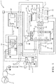
- Fig. 1 illustrates a resistance soldering system 10, hereafter referred to as the system 10.
- the system 10 is beneficial because the system 10 controls a power delivered to a solder joint (not shown) for a specified time to melt the solder joint.
- the system 10 includes a power input channel 12 receiving an alternating current 14 from a power source (e.g. a power receptacle connected to a power grid not shown).
- the power source may be any power source, and in the example illustrated in Fig. 1 is a 120 volt AC (120VAC) power source.
- the system 10 also includes an AC to DC converter 16 (AC/DC converter 16) in electrical communication with the power input channel 12.
- the AC/DC converter 16 converts a portion of the alternating current 14 to a direct current 18 at a converter output 20.
- the AC/DC converter 16 may be any type of AC/DC converter, and in the example illustrated in Fig. 1 generates an output voltage of about 24VDC.
- the system 10 also includes one or more controller circuits 22 in electrical communication with the converter output 20.
- the one or more controller circuits 22 control a signal 24 indicative of a desired power level 26 delivered for a desired time 28.
- the signal 24 is a current signal in a range of 0mA to 20mA.
- the signal 24 a voltage signal.
- the one or more controller circuits 22 may include a processor (not shown) such as a microprocessor or other control circuitry such as analog and/or digital control circuitry including an application specific integrated circuit (ASIC) for processing data as should be evident to those in the art.
- ASIC application specific integrated circuit
- the one or more controller circuits 22 include a memory 30, including non volatile memory, such as electrically erasable programmable read only memory (EEPROM) for storing one or more routines, thresholds, and captured data.
- the one or more routines may be executed by the processors to perform steps for controlling the signal 24 as described above.
- the one or more controller circuits 22 may be distributed throughout the system 10 and communicate with one another through a wiring harness (not specifically shown), or may be housed in a common enclosure.
- the one or more controller circuits 22 may be separate circuity, be the same circuitry, subsystems of one another, or any combination thereof.
- the functions performed by the one or more controller circuits 22 may be handled by each individual controller circuit 22 or distributed between them, e.g., load balancing.
- the system 10 also includes a silicon-controlled rectifier 32 (SCR 32) in electrical communication with the power input channel 12, the converter output 20, and the signal 24.
- SCR 32 controls an SCR output voltage 34 to a SCR output channel 36, wherein the SCR output voltage 34 is proportional to the signal 24.
- the SCR 32 may be any phase angle operated SCR 32 suitable for the application.
- One such SCR 32 is the UF1HXTE0 08 PIR0Z manufactured by Control Concepts, Inc. of Chanhassen, Minnesota, USA.
- the SCR output voltage 34 is OVAC to 120VAC.
- the system 10 also includes a transformer 38 having a primary side 40 and a secondary side 42.
- the primary side 40 is in electrical communication with the SCR output channel 36 and receives the 0VAC to 120VAC potential from the SCR 32 as described above.
- the transformer 38 reduces (i.e. steps down) the SCR output voltage 34 from the primary side 40 (e.g. 120VAC) to a secondary voltage 44 on the secondary side 42.
- the transformer 38 may be any transformer 38 that reduces the SCR output voltage 34, and in the example illustrated in Fig. 1 , reduces the SCR output voltage 34 to a range of 0VAC to about 5VAC.
- the system 10 also includes a pair of output leads 46 in electrical communication with poles of the secondary side 42 of the transformer 38.
- the pair of output leads 46 are configured to apply the secondary voltage 44 to the solder joint disposed between the pair of output leads 46.
- the pair of output leads 46 may terminate at corresponding electrodes (not shown) that contact the solder joint and are preferably formed of a carbon based material, such as graphite.
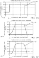
- Figs. 2A 2C are plots illustrating examples of the desired power level 26 applied to the solder joint for the desired time 28.
- the one or more controller circuits 22 determine the signal 24 applied to the SCR 32 required to melt the solder joint based on the desired power level 26 and the desired time 28, thereby melting the solder joint disposed between the pair of output leads 46. It will be appreciated that the total energy applied to the solder joint is indicated by an area beneath the curves of each plot, and in the examples illustrated in Figs. 2A 2C has units of Watt seconds (W s).
- the one or more controller circuits 22 may be programmed with specific ramp rates and/or dwell times based on characteristics of the solder joint including geometric dimensions, solder alloy composition, and materials being joined by the solder.
- the one or more controller circuits 22 controls the desired power level 26 independent of the desired time 28. This is in contrast to prior art resistance soldering systems that typically require a total energy input be commanded, wherein the time to deliver the energy varies based on a quality of the electrical connection between the contacts and the solder joint.
- the system 10 is an improvement over prior art resistance soldering systems because the system 10 adds another degree of freedom to the resistance soldering process, i.e., the desired time 28.
- the one or more controller circuits 22 controls the desired time 28 independent of the desired power level 26.
- the desired power level 26 is characterized by a linear function 48 and/or a piece wise linear function 50.
- the desired power level 26 is characterized by a polynomial function 52. Soldering profiles containing the desired power level 26 and the desired time 28 are user defined and based on the characteristics of the solder joint as described above.
- the SCR 32 further includes a voltage output signal 54 and a current output signal 56 in electrical communication with the one or more controller circuits 22.
- the voltage output signal 54 and the current output signal 56 are indicative of a total power delivered 58 to the primary side 40 of the transformer 38. That is, the voltage output signal 54 and the current output signal 56 are scaled by the one or more controller circuits 22 to determine the total power delivered 58 to the primary side 40 of the transformer 38, and both are characterized by electrical currents in the range of 4mA to 20mA.
- the one or more controller circuits 22 determine the total power delivered 58 to the pair of output leads 46 based on the voltage output signal 54 and the current output signal 56, and may also take into account any electrical efficiency losses through the transformer 38 and/or wiring.
- the system 10 stores the voltage output signal 54 and the current output signal 56 in the memory 30 of the one or more controller circuits 22 for historical purposes and may be accessed by an operator.
- the system 10 also includes a visual display 60 that is a component of a human machine interface (HMI - not specifically shown).
- the voltage output signal 54 and the current output signal 56 are displayed on the visual display 60 for viewing by the operator and may be used for quality control purposes.
- Figs. 3 4 illustrate additional details of the one or more controller circuits that are used in the system 10.
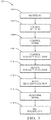
- Fig. 5 is a flow chart illustrating another embodiment of a method 100 of operating a resistance soldering system 10, hereafter referred to as the system 10.
- Step 102 RECEIVE AC, includes receiving an alternating current 14 from a power source with a power input channel 12 as described above and illustrated in Fig. 1 .
- Step 104 CONVERT AC TO DC, includes converting a portion of the alternating current 14 to a direct current 18 at a converter output 20 with an AC to DC converter 16 (AC/DC converter 16) in electrical communication with the power input channel 12 as described above and illustrated in Fig. 1 .
- AC/DC converter 16 AC to DC converter 16
- Step 106 includes controlling a signal 24 indicative of a desired power level 26 delivered for a desired time 28 with one or more controller circuits 22 in electrical communication with the converter output 20.
- the signal 24 is a current signal in a range of 0mA to 20mA, and in another embodiment (not shown), the signal 24 is a voltage signal.
- the one or more controller circuits 22 controls the desired power level 26 independent of the desired time 28, and controls the desired time 28 independent of the desired power level 26.
- Step 108 CONTROL SCR OUTPUT VOLTAGE, includes controlling an SCR output voltage 34 to a SCR output channel 36 proportional to the signal 24 with a silicon-controlled rectifier 32 (SCR 32) as described above.
- the SCR output voltage 34 is 0VAC to 120VAC.
- the SCR 32 further includes a voltage output signal 54 and a current output signal 56 that are indicative of a total power delivered 58 to a primary side 40 of a transformer 38, as described above and illustrated in Fig. 1 .
- Step 110 REDUCE SCR OUTPUT VOLTAGE, includes reducing, with the transformer 38 the SCR output voltage 34 from the primary side 40 to a secondary voltage 44 on a secondary side 42 of the transformer 38 as described above.
- the transformer 38 may be any transformer 38 that reduces the SCR output voltage 34, and preferably reduces the SCR output voltage 34 to a range of 0VAC to about 5VAC as described above.
- Step 112 APPLY SECONDARY VOLTAGE, includes applying, with a pair of output leads 46 in electrical communication with poles of the secondary side 42 of the transformer 38, the secondary voltage 44 to a solder joint disposed between the pair of output leads 46.
- the pair of output leads 46 may terminate at corresponding electrodes that contact the solder joint and are preferably formed of a carbon based material, such as graphite.
- Step 114, DETERMINE SIGNAL includes determining, with the one or more controller circuits 22, the signal 24 applied to the SCR 32 required to melt the solder joint based on the desired power level 26 and the desired time 28.
- Figs. 2A 2B illustrate the desired power level 26 characterized by a linear function 48 and/or a piece wise linear function 50.
- the desired power level 26 is characterized by a polynomial function 52.
- the voltage output signal 54 and the current output signal 56 that are indicative of the total power delivered 58 to the primary side 40 of the transformer 38 are stored in a memory 30 of the one or more controller circuits 22 as described above.
- the voltage output signal 54 and the current output signal 56 are displayed on a visual display 60 for viewing by an operator and may be used for quality control purposes, as described above.
- Step 116 MELT SOLDER JOINT, includes melting the solder joint disposed between the pair of output leads 46 with the secondary voltage 44 as described above.
- a resistance soldering system 10 (the system 10) and a method 100 of operating the system 10 are provided.
- the system 10 is an improvement over prior art resistance soldering systems because the system 10 controls the desired power level 26 independent of the desired time 28.
- first contact could be termed a second contact
- second contact could be termed a first contact
- the first contact and the second contact are both contacts, but they are not the same contact.
- the terminology used in the description of the various described embodiments herein is for the purpose of describing particular embodiments only and is not intended to be limiting. As used in the description of the various described embodiments and the appended claims, the singular forms "a”, “an” and “the” are intended to include the plural forms as well, unless the context clearly indicates otherwise. It will also be understood that the term “and/or” as used herein refers to and encompasses any and all possible combinations of one or more of the associated listed items.
- the phrase “if it is determined” or “if [a stated condition or event] is detected” is, optionally, construed to mean “upon determining” or “in response to determining” or “upon detecting [the stated condition or event]” or “in response to detecting [the stated condition or event],” depending on the context.
Landscapes
- Engineering & Computer Science (AREA)
- Mechanical Engineering (AREA)
- Physics & Mathematics (AREA)
- General Physics & Mathematics (AREA)
- Automation & Control Theory (AREA)
- Rectifiers (AREA)
- Dc-Dc Converters (AREA)
- Electric Connection Of Electric Components To Printed Circuits (AREA)
- Arc Welding Control (AREA)
- Generation Of Surge Voltage And Current (AREA)
- Control Of Voltage And Current In General (AREA)
Abstract
Description
- This disclosure generally relates to a soldering system, and more particularly relates to a resistance soldering system as well as to a method of operating a resistance soldering system.
- It is known to solder electric components using a resistance soldering process. A quality of a solder joint is affected by a total amount of energy applied during the resistance soldering process.
- The present disclosure proposes to solve the above mentioned problem by providing a resistance soldering system according to
claim 1 and a method of operating a resistance soldering system according toclaim 10. Embodiments are subject of the dependent claims. - In accordance with one example, a resistance soldering system includes a power input channel, an AC to DC converter, one or more controller circuits, a silicon-controlled rectifier, a transformer, and a pair of output leads. The power input channel receives an alternating current from a power source. The AC to DC converter is in electrical communication with the power input channel. The AC to DC converter converts a portion of the alternating current to a direct current at a converter output. The one or more controller circuits are in electrical communication with the converter output. The one or more controller circuits control a signal indicative of a desired power level delivered for a desired time. The silicon-controlled rectifier (SCR) is in electrical communication with the power input channel, the converter output, and the signal. The SCR controls an SCR output voltage to an SCR output channel proportional to the signal. The transformer has a primary side and a secondary side. The primary side is in electrical communication with the SCR output channel. The transformer reduces the SCR output voltage from the primary side to a secondary voltage on the secondary side. The pair of output leads are in electrical communication with poles of the secondary side of the transformer. The pair of output leads are configured to apply the secondary voltage to a solder joint disposed between the pair of output leads. The one or more controller circuits determine the signal applied to the SCR that is required to melt the solder joint based on the desired power level and the desired time, thereby melting the solder joint disposed between the pair of output leads.
- According to examples:
- the signal is a current signal;
- the signal is a voltage signal;
- the silicon-controlled rectifier further includes a voltage output signal and a current output signal in electrical communication with the one or more controller circuits, the voltage output signal and the current output signal indicative of a total power delivered to the primary side of the transformer, whereby the one or more controller circuits determine the total power delivered to the pair of output leads based on the voltage output signal and the current output signal;
- the voltage output signal and the current output signal are stored in a memory of the one or more controller circuits;
- the system further includes a visual display, and the voltage output signal and the current output signal are displayed on the visual display;
- the one or more controller circuits controls the desired power level independent of the desired time;
- the one or more controller circuits controls the desired time independent of the desired power level;
- the desired power level is characterized by a linear function;
- the linear function is further characterized by a piece wise linear function;
- the desired power level is characterized by a polynomial function;
- According to an example, a method of operating a resistance soldering system comprises the steps of:
- a) receiving an alternating current from a power source with a power input channel;
- b) converting a portion of the alternating current to a direct current at a converter output with an AC to DC converter in electrical communication with the power input channel;
- c) controlling a signal indicative of a desired power level delivered for a desired time with one or more controller circuits in electrical communication with the converter output;
- d) controlling an SCR output voltage to a SCR output channel proportional to the signal with a silicon-controlled rectifier in electrical communication with the power input channel, the converter output, and the signal;
- e) reducing, with a transformer having a primary side and a secondary side, the primary side in electrical communication with the SCR output channel, the SCR output voltage from the primary side to a secondary voltage on the secondary side;
- f) applying, with a pair of output leads in electrical communication with poles of the secondary side of the transformer, the secondary voltage to a solder joint disposed between the pair of output leads; and
- g) determining, with the one or more controller circuits, the signal applied to the silicon-controlled rectifier required to melt the solder joint based on the desired power level and the desired time, thereby melting the solder joint disposed between the pair of output leads.
- According to examples, the method further comprises:
- the signal is a current signal;
- the signal is a voltage signal;
- the silicon-controlled rectifier further includes a voltage output signal and a current output signal in electrical communication with the one or more controller circuits, the voltage output signal and the current output signal indicative of a total power delivered to the primary side of the transformer, further including the step of determining, with the one or more controller circuits, the total power delivered to the pair of output leads based on the voltage output signal and the current output signal;
- the one or more controller circuits controls the desired power level independent of the desired time;
- the one or more controller circuits controls the desired time independent of the desired power level;
- the desired power level is characterized by a linear function;
- the linear function is further characterized by a piece wise linear function;
- the desired power level is characterized by a polynomial function.
- According to an example, the method further comprises the step of:
h) storing the voltage output signal and the current output signal in a memory of the one or more controller circuits. - According to an example, the method further comprises the step of:
i) displaying the voltage output signal and the current output signal on a visual display. - The present invention will now be described, by way of example with reference to the accompanying drawings, in which:
-
Fig. 1 is a schematic diagram of a resistance soldering system in accordance with one embodiment; -
Fig. 2A is a graph illustrating a power delivered over time by the resistance soldering system ofFig. 1 in accordance with one embodiment; -
Fig. 2B is another plot illustrating the power delivered over time by the resistance soldering system ofFig. 1 in accordance with one embodiment; -
Fig. 2C is yet another plot illustrating the power delivered over time by the resistance soldering system ofFig. 1 in accordance with one embodiment; -
Fig. 3 is a schematic diagram of a controller circuit of the resistance soldering system ofFig. 1 in accordance with one embodiment; -
Fig. 4 is a schematic diagram of another controller circuit of the resistance soldering system ofFig. 1 in accordance with a different embodiment; and -
Fig. 5 is a flow chart illustrating a method of operating the resistance soldering system ofFig. 1 in accordance with another embodiment. - Reference will now be made in detail to embodiments, examples of which are illustrated in the accompanying drawings. In the following detailed description, numerous specific details are set forth in order to provide a thorough understanding of the various described embodiments. However, it will be apparent to one of ordinary skill in the art that the various described embodiments may be practiced without these specific details. In other instances, well known methods, procedures, components, circuits, and networks have not been described in detail so as not to unnecessarily obscure aspects of the embodiments.
-
Fig. 1 illustrates aresistance soldering system 10, hereafter referred to as thesystem 10. As will be described in more detail herein, thesystem 10 is beneficial because thesystem 10 controls a power delivered to a solder joint (not shown) for a specified time to melt the solder joint. Thesystem 10 includes apower input channel 12 receiving an alternating current 14 from a power source (e.g. a power receptacle connected to a power grid not shown). The power source may be any power source, and in the example illustrated inFig. 1 is a 120 volt AC (120VAC) power source. - The
system 10 also includes an AC to DC converter 16 (AC/DC converter 16) in electrical communication with thepower input channel 12. The AC/DC converter 16 converts a portion of the alternating current 14 to a direct current 18 at aconverter output 20. The AC/DC converter 16 may be any type of AC/DC converter, and in the example illustrated inFig. 1 generates an output voltage of about 24VDC. - The
system 10 also includes one ormore controller circuits 22 in electrical communication with theconverter output 20. The one ormore controller circuits 22 control asignal 24 indicative of a desiredpower level 26 delivered for a desiredtime 28. In the example illustrated inFig. 1 , thesignal 24 is a current signal in a range of 0mA to 20mA. In another embodiment (not shown), the signal 24 a voltage signal. The one ormore controller circuits 22 may include a processor (not shown) such as a microprocessor or other control circuitry such as analog and/or digital control circuitry including an application specific integrated circuit (ASIC) for processing data as should be evident to those in the art. The one ormore controller circuits 22 include amemory 30, including non volatile memory, such as electrically erasable programmable read only memory (EEPROM) for storing one or more routines, thresholds, and captured data. The one or more routines may be executed by the processors to perform steps for controlling thesignal 24 as described above. The one ormore controller circuits 22 may be distributed throughout thesystem 10 and communicate with one another through a wiring harness (not specifically shown), or may be housed in a common enclosure. As will be appreciated, the one ormore controller circuits 22 may be separate circuity, be the same circuitry, subsystems of one another, or any combination thereof. As also will be appreciated, the functions performed by the one ormore controller circuits 22 may be handled by eachindividual controller circuit 22 or distributed between them, e.g., load balancing. - The
system 10 also includes a silicon-controlled rectifier 32 (SCR 32) in electrical communication with thepower input channel 12, theconverter output 20, and thesignal 24. TheSCR 32 controls anSCR output voltage 34 to aSCR output channel 36, wherein theSCR output voltage 34 is proportional to thesignal 24. TheSCR 32 may be any phase angle operatedSCR 32 suitable for the application. Onesuch SCR 32 is the UF1HXTE0 08 PIR0Z manufactured by Control Concepts, Inc. of Chanhassen, Minnesota, USA. In the example illustrated inFig. 1 , theSCR output voltage 34 is OVAC to 120VAC. - The
system 10 also includes atransformer 38 having a primary side 40 and asecondary side 42. The primary side 40 is in electrical communication with theSCR output channel 36 and receives the 0VAC to 120VAC potential from theSCR 32 as described above. Thetransformer 38 reduces (i.e. steps down) theSCR output voltage 34 from the primary side 40 (e.g. 120VAC) to asecondary voltage 44 on thesecondary side 42. Thetransformer 38 may be anytransformer 38 that reduces theSCR output voltage 34, and in the example illustrated inFig. 1 , reduces theSCR output voltage 34 to a range of 0VAC to about 5VAC. - The
system 10 also includes a pair of output leads 46 in electrical communication with poles of thesecondary side 42 of thetransformer 38. The pair of output leads 46 are configured to apply thesecondary voltage 44 to the solder joint disposed between the pair of output leads 46. The pair of output leads 46 may terminate at corresponding electrodes (not shown) that contact the solder joint and are preferably formed of a carbon based material, such as graphite. -
Figs. 2A 2C are plots illustrating examples of the desiredpower level 26 applied to the solder joint for the desiredtime 28. The one ormore controller circuits 22 determine thesignal 24 applied to theSCR 32 required to melt the solder joint based on the desiredpower level 26 and the desiredtime 28, thereby melting the solder joint disposed between the pair of output leads 46. It will be appreciated that the total energy applied to the solder joint is indicated by an area beneath the curves of each plot, and in the examples illustrated inFigs. 2A 2C has units of Watt seconds (W s). The one ormore controller circuits 22 may be programmed with specific ramp rates and/or dwell times based on characteristics of the solder joint including geometric dimensions, solder alloy composition, and materials being joined by the solder. The one ormore controller circuits 22 controls the desiredpower level 26 independent of the desiredtime 28. This is in contrast to prior art resistance soldering systems that typically require a total energy input be commanded, wherein the time to deliver the energy varies based on a quality of the electrical connection between the contacts and the solder joint. Thesystem 10 is an improvement over prior art resistance soldering systems because thesystem 10 adds another degree of freedom to the resistance soldering process, i.e., the desiredtime 28. Accordingly, the one ormore controller circuits 22 controls the desiredtime 28 independent of the desiredpower level 26. As illustrated inFigs. 2A 2B , the desiredpower level 26 is characterized by alinear function 48 and/or a piece wiselinear function 50. As illustrated inFig. 2C , the desiredpower level 26 is characterized by apolynomial function 52. Soldering profiles containing the desiredpower level 26 and the desiredtime 28 are user defined and based on the characteristics of the solder joint as described above. - Referring back to
Fig. 1 , theSCR 32 further includes avoltage output signal 54 and acurrent output signal 56 in electrical communication with the one ormore controller circuits 22. Thevoltage output signal 54 and thecurrent output signal 56 are indicative of a total power delivered 58 to the primary side 40 of thetransformer 38. That is, thevoltage output signal 54 and thecurrent output signal 56 are scaled by the one ormore controller circuits 22 to determine the total power delivered 58 to the primary side 40 of thetransformer 38, and both are characterized by electrical currents in the range of 4mA to 20mA. The one ormore controller circuits 22 determine the total power delivered 58 to the pair of output leads 46 based on thevoltage output signal 54 and thecurrent output signal 56, and may also take into account any electrical efficiency losses through thetransformer 38 and/or wiring. Thesystem 10 stores thevoltage output signal 54 and thecurrent output signal 56 in thememory 30 of the one ormore controller circuits 22 for historical purposes and may be accessed by an operator. - The
system 10 also includes avisual display 60 that is a component of a human machine interface (HMI - not specifically shown). Thevoltage output signal 54 and thecurrent output signal 56 are displayed on thevisual display 60 for viewing by the operator and may be used for quality control purposes. -
Figs. 3 4 illustrate additional details of the one or more controller circuits that are used in thesystem 10. -
Fig. 5 is a flow chart illustrating another embodiment of amethod 100 of operating aresistance soldering system 10, hereafter referred to as thesystem 10. -
Step 102, RECEIVE AC, includes receiving an alternating current 14 from a power source with apower input channel 12 as described above and illustrated inFig. 1 . -
Step 104, CONVERT AC TO DC, includes converting a portion of the alternating current 14 to a direct current 18 at aconverter output 20 with an AC to DC converter 16 (AC/DC converter 16) in electrical communication with thepower input channel 12 as described above and illustrated inFig. 1 . -
Step 106, CONTROL SIGNAL, includes controlling asignal 24 indicative of a desiredpower level 26 delivered for a desiredtime 28 with one ormore controller circuits 22 in electrical communication with theconverter output 20. In the example illustrated inFig. 1 , thesignal 24 is a current signal in a range of 0mA to 20mA, and in another embodiment (not shown), thesignal 24 is a voltage signal. The one ormore controller circuits 22 controls the desiredpower level 26 independent of the desiredtime 28, and controls the desiredtime 28 independent of the desiredpower level 26. -
Step 108, CONTROL SCR OUTPUT VOLTAGE, includes controlling anSCR output voltage 34 to aSCR output channel 36 proportional to thesignal 24 with a silicon-controlled rectifier 32 (SCR 32) as described above. In the example illustrated inFig. 1 , theSCR output voltage 34 is 0VAC to 120VAC. TheSCR 32 further includes avoltage output signal 54 and acurrent output signal 56 that are indicative of a total power delivered 58 to a primary side 40 of atransformer 38, as described above and illustrated inFig. 1 . -
Step 110, REDUCE SCR OUTPUT VOLTAGE, includes reducing, with thetransformer 38 theSCR output voltage 34 from the primary side 40 to asecondary voltage 44 on asecondary side 42 of thetransformer 38 as described above. Thetransformer 38 may be anytransformer 38 that reduces theSCR output voltage 34, and preferably reduces theSCR output voltage 34 to a range of 0VAC to about 5VAC as described above. -
Step 112, APPLY SECONDARY VOLTAGE, includes applying, with a pair of output leads 46 in electrical communication with poles of thesecondary side 42 of thetransformer 38, thesecondary voltage 44 to a solder joint disposed between the pair of output leads 46. The pair of output leads 46 may terminate at corresponding electrodes that contact the solder joint and are preferably formed of a carbon based material, such as graphite. -
Step 114, DETERMINE SIGNAL, includes determining, with the one ormore controller circuits 22, thesignal 24 applied to theSCR 32 required to melt the solder joint based on the desiredpower level 26 and the desiredtime 28.Figs. 2A 2B , illustrate the desiredpower level 26 characterized by alinear function 48 and/or a piece wiselinear function 50. As illustrated inFig. 2C , the desiredpower level 26 is characterized by apolynomial function 52. Thevoltage output signal 54 and thecurrent output signal 56 that are indicative of the total power delivered 58 to the primary side 40 of thetransformer 38 are stored in amemory 30 of the one ormore controller circuits 22 as described above. Thevoltage output signal 54 and thecurrent output signal 56 are displayed on avisual display 60 for viewing by an operator and may be used for quality control purposes, as described above. -
Step 116, MELT SOLDER JOINT, includes melting the solder joint disposed between the pair of output leads 46 with thesecondary voltage 44 as described above. - Accordingly, a resistance soldering system 10 (the system 10) and a
method 100 of operating thesystem 10 are provided. Thesystem 10 is an improvement over prior art resistance soldering systems because thesystem 10 controls the desiredpower level 26 independent of the desiredtime 28. - While this invention has been described in terms of the preferred embodiments thereof, it is not intended to be so limited, but rather only to the extent set forth in the claims that follow. "One or more" includes a function being performed by one element, a function being performed by more than one element, e.g., in a distributed fashion, several functions being performed by one element, several functions being performed by several elements, or any combination of the above. It will also be understood that, although the terms first, second, etc. are, in some instances, used herein to describe various elements, these elements should not be limited by these terms. These terms are only used to distinguish one element from another. For example, a first contact could be termed a second contact, and, similarly, a second contact could be termed a first contact, without departing from the scope of the various described embodiments. The first contact and the second contact are both contacts, but they are not the same contact. The terminology used in the description of the various described embodiments herein is for the purpose of describing particular embodiments only and is not intended to be limiting. As used in the description of the various described embodiments and the appended claims, the singular forms "a", "an" and "the" are intended to include the plural forms as well, unless the context clearly indicates otherwise. It will also be understood that the term "and/or" as used herein refers to and encompasses any and all possible combinations of one or more of the associated listed items. It will be further understood that the terms "includes," "including," "comprises," and/or "comprising," when used in this specification, specify the presence of stated features, integers, steps, operations, elements, and/or components, but do not preclude the presence or addition of one or more other features, integers, steps, operations, elements, components, and/or groups thereof. As used herein, the term "if' is, optionally, construed to mean "when" or "upon" or "in response to determining" or "in response to detecting," depending on the context. Similarly, the phrase "if it is determined" or "if [a stated condition or event] is detected" is, optionally, construed to mean "upon determining" or "in response to determining" or "upon detecting [the stated condition or event]" or "in response to detecting [the stated condition or event]," depending on the context.
Claims (15)
- A resistance soldering system (10), comprising:a power input (12) configured to receive an alternating current from a power source;a controller circuit (22) configured to generate a control signal (24) indicative of a desired power level (26) delivered for a desired time (28);a silicon-controlled rectifier (32) electrically connected to the power input (12) and the controller circuit (22) and configured to produce a control voltage (34) proportional to the control signal (24);a transformer (38) having a primary side (40) configured to receive the control voltage (34) from the silicon-controlled rectifier (32) and a secondary side (42) having output leads (46) configured to apply an output voltage to a solder joint disposed between the output leads (46),wherein the controller circuit (22) determines the control signal (24) applied to the silicon-controlled rectifier (32) required to melt the solder joint based on the desired power level (26) and the desired time (28) and wherein the controller circuit (22) controls the desired power level (26) independent of the desired time (28).
- The system (10) in accordance with claim 1, wherein the control signal (24) is a current signal.
- The system (10) in accordance with claim 1, wherein the control signal (24) is a voltage signal.
- The system (10) in accordance with claim 1, wherein the silicon-controlled rectifier (32) receives a voltage output signal (54) and a current output signal (56) from the controller circuit (22), the voltage output signal (54) and the current output signal (56) indicative of a total power (58) delivered to the primary side (40) of the transformer (38), whereby the controller circuit (22) determines the total power (58) delivered to a pair of output leads (46) based on the voltage output signal (54) and the current output signal (56).
- The system (10) in accordance with claim 4, wherein the voltage output signal (54) and the current output signal (56) are stored in a memory (30) of the controller circuit (22).
- The system (10) in accordance with claim 4, wherein the system (10) further includes a visual display (60) and wherein the voltage output signal (54) and the current output signal (56) are displayed on the visual display (60).
- The system (10) in accordance with claim 1, wherein the desired power level (26) is characterized as a linear function (48).
- The system (10) in accordance with claim 7, wherein the linear function (48) is further characterized as a piece-wise linear function (50).
- The system (10) in accordance with claim 1, wherein the desired power level (26) is characterized as a polynomial function (52).
- A method (100) of operating a resistance soldering system (10), comprising:receiving an alternating current (14) from a power source;generating a control signal (24) indicative of a desired power level (26) delivered for a desired time (28) via a controller circuit (22);producing a control voltage (34) proportional to the control signal (24) via a silicon-controlled rectifier (32) electrically connected to the power source (12) and the controller circuit (22);producing an output voltage from a transformer (38) having a primary side (40) and a secondary side (42) as the primary side (40) receives the control voltage (34) from the silicon-controlled rectifier (32);applying the output voltage to a solder joint disposed between output leads (46) electrically connected to the secondary side (42); anddetermining, via the controller circuit (22), the signal (24) applied to the silicon-controlled rectifier (32) required to melt the solder joint based on the desired power level (26) and the desired time (28), wherein the controller circuit (22) controls the desired time (28) independent of the desired power level (26).
- The method (100) in accordance with claim 10, wherein the control signal (24) is a current signal.
- The method (100) in accordance with claim 10, wherein the control signal (24) is a voltage signal.
- The method (100) in accordance with claim 10, wherein the silicon-controlled rectifier (32) receives a voltage output signal (54) and a current output signal (56) from the controller circuit (22), wherein the voltage output signal (54) and the current output signal (56) are indicative of a total power (58) delivered to the primary side (40) of the transformer (38), and wherein the method (100) further includes:
determining the total power (58) delivered to a pair of output leads (46) based on the voltage output signal (54) and the current output signal (56) via the controller circuit (22). - The method (100) in accordance with claim 13, further including storing the voltage output signal (54) and the current output signal (56) in a memory (30) of the controller circuit (22).
- The method (100) in accordance with claim 13, wherein the method (100) further includes:providing a visual display (60); anddisplaying the voltage output signal (54) and the current output signal (56) on the visual display (60).
Applications Claiming Priority (2)
| Application Number | Priority Date | Filing Date | Title |
|---|---|---|---|
| US16/012,919 US10926346B2 (en) | 2018-06-20 | 2018-06-20 | Resistance soldering system |
| EP19180542.3A EP3620252B1 (en) | 2018-06-20 | 2019-06-17 | Resistance soldering system and method |
Related Parent Applications (2)
| Application Number | Title | Priority Date | Filing Date |
|---|---|---|---|
| EP19180542.3A Division EP3620252B1 (en) | 2018-06-20 | 2019-06-17 | Resistance soldering system and method |
| EP19180542.3A Division-Into EP3620252B1 (en) | 2018-06-20 | 2019-06-17 | Resistance soldering system and method |
Publications (2)
| Publication Number | Publication Date |
|---|---|
| EP3878588A1 true EP3878588A1 (en) | 2021-09-15 |
| EP3878588B1 EP3878588B1 (en) | 2023-05-10 |
Family
ID=66912696
Family Applications (2)
| Application Number | Title | Priority Date | Filing Date |
|---|---|---|---|
| EP19180542.3A Active EP3620252B1 (en) | 2018-06-20 | 2019-06-17 | Resistance soldering system and method |
| EP21165445.4A Active EP3878588B1 (en) | 2018-06-20 | 2019-06-17 | Resistance soldering system and method of operating a resistance soldering system |
Family Applications Before (1)
| Application Number | Title | Priority Date | Filing Date |
|---|---|---|---|
| EP19180542.3A Active EP3620252B1 (en) | 2018-06-20 | 2019-06-17 | Resistance soldering system and method |
Country Status (5)
| Country | Link |
|---|---|
| US (2) | US10926346B2 (en) |
| EP (2) | EP3620252B1 (en) |
| JP (1) | JP2020032460A (en) |
| KR (1) | KR102229816B1 (en) |
| CN (2) | CN113843487B (en) |
Citations (3)
| Publication number | Priority date | Publication date | Assignee | Title |
|---|---|---|---|---|
| NL8503353A (en) * | 1985-12-05 | 1987-07-01 | Weld Equip Bv | Electronic system controlling welding or reflow-soldering - has programmed microprocessor to select, apply and control energy, temp. and weld-solder electrode pressure |
| JPH1154905A (en) * | 1997-08-05 | 1999-02-26 | Nippon Avionics Co Ltd | Pulse heating type bonding apparatus and its control method |
| US20010027962A1 (en) * | 2000-03-22 | 2001-10-11 | Kyoji Moro | Metallic members joining method and reflow soldering method |
Family Cites Families (31)
| Publication number | Priority date | Publication date | Assignee | Title |
|---|---|---|---|---|
| CA783737A (en) | 1968-04-23 | A. Burton Charles | Resistance soldering apparatus | |
| US2790059A (en) | 1955-06-13 | 1957-04-23 | Zepher Mfg Co | Resistance soldering device and method |
| US2969449A (en) | 1959-08-25 | 1961-01-24 | Jonathan E Tyler | Resistance soldering power supply |
| US3379896A (en) | 1964-09-03 | 1968-04-23 | Electro Miniatures Corp | Automatic resistance soldering apparatus and the like |
| US3366920A (en) | 1965-11-22 | 1968-01-30 | Amp Inc | Coaxial connector |
| US3605236A (en) | 1968-12-11 | 1971-09-20 | Burndy Corp | Assembling and positioning device for coaxial electrical contacts |
| US3621193A (en) | 1970-09-21 | 1971-11-16 | Nasa | Positive contact resistance soldering unit |
| US3778581A (en) * | 1972-08-03 | 1973-12-11 | Hughes Aircraft Co | Time-at-temperature a-c reflow soldering power supply |
| US3962562A (en) | 1974-01-14 | 1976-06-08 | Burroughs Corporation | Resistance solder unit control |
| GB2066591B (en) | 1979-12-13 | 1983-12-21 | Bunker Ramo | Electrical connector shell and method of making same |
| US4388515A (en) * | 1981-03-19 | 1983-06-14 | Pertron Controls Corporation | Resistance welding control system |
| DE9204968U1 (en) | 1992-04-09 | 1992-08-27 | Siemens AG, 8000 München | Shielding arrangement for openings in housing walls of RF-tight housings |
| EP0688626B1 (en) * | 1994-05-27 | 2000-02-16 | Kabushiki Kaisha Toshiba | Control equipment for resistance welding machine |
| US6013892A (en) * | 1998-01-27 | 2000-01-11 | Square D Company | Resistance weld control with line impedance compensation |
| US6326580B1 (en) * | 1999-08-23 | 2001-12-04 | Miyachi Technos Corporation | Joining apparatus |
| WO2002007312A2 (en) * | 2000-07-13 | 2002-01-24 | Isothermal Systems Research, Inc. | Power semiconductor switching devices, power converters, integrated circuit assemblies, integrated circuitry, power current switching methods, methods of forming a power semiconductor switching device, power conversion methods, power semiconductor switching device packaging methods, and methods of forming a power transistor |
| FR2821682B1 (en) * | 2001-03-01 | 2003-05-30 | Usinor | METHOD FOR MONITORING AND CONTROLLING A TECHNICAL PROCESS |
| JP2003071560A (en) | 2001-08-30 | 2003-03-11 | Mitsubishi Heavy Ind Ltd | Brazing device for stellite of turbine blade |
| KR100907651B1 (en) * | 2002-12-23 | 2009-07-14 | 주식회사 포스코 | Constant power controller and method for resistance welding machine |
| US7727018B2 (en) | 2008-04-22 | 2010-06-01 | Tyco Electronics Corporation | EMI gasket for an electrical connector assembly |
| WO2010030622A1 (en) | 2008-09-09 | 2010-03-18 | Molex Incorporated | Connector with impedance tuned terminal arrangement |
| US8147272B2 (en) | 2010-02-04 | 2012-04-03 | Tyco Electronics Corporation | Header connector assembly |
| US9035626B2 (en) * | 2010-08-18 | 2015-05-19 | Volterra Semiconductor Corporation | Switching circuits for extracting power from an electric power source and associated methods |
| CN202741914U (en) * | 2012-06-25 | 2013-02-20 | 应城骏腾发自动焊接装备有限公司 | Intermediate-frequency-inversion direct-current welding power supply |
| CN103008865B (en) * | 2012-12-31 | 2015-02-04 | 天津商科数控设备有限公司 | Process method for pulse width-adjustable AC (Alternating Current)-DC (Direct Current) inverter resistance welding |
| EP2843774B1 (en) | 2013-08-26 | 2016-05-25 | Delphi Technologies, Inc. | Electromagnetic shielding assembly for an electrical high power connector assembly |
| US20160175968A1 (en) * | 2014-12-19 | 2016-06-23 | Illinois Tool Works Inc. | Method and apparatus for providing welding and auxiliary power |
| US9808881B2 (en) * | 2015-03-03 | 2017-11-07 | Illinois Tool Works Inc. | Method and apparatus for providing welding and auxiliary power |
| US9413115B1 (en) | 2015-05-14 | 2016-08-09 | Tyco Electronics Corporation | EMI gasket for electrical connector assembly |
| EP3107155B8 (en) | 2015-06-16 | 2019-01-16 | Aptiv Technologies Limited | Electrical connector system with shielding sleeve and method thereof |
| EP3220483A1 (en) | 2016-03-17 | 2017-09-20 | TE Connectivity Germany GmbH | Electric connection device, method of assembling an electrical cable and assembled electrical coaxial cable |
-
2018
- 2018-06-20 US US16/012,919 patent/US10926346B2/en active Active
-
2019
- 2019-06-17 EP EP19180542.3A patent/EP3620252B1/en active Active
- 2019-06-17 KR KR1020190071644A patent/KR102229816B1/en active Active
- 2019-06-17 EP EP21165445.4A patent/EP3878588B1/en active Active
- 2019-06-19 CN CN202111115027.1A patent/CN113843487B/en active Active
- 2019-06-19 CN CN201910531588.6A patent/CN110614419B/en active Active
- 2019-06-19 JP JP2019113299A patent/JP2020032460A/en active Pending
-
2021
- 2021-01-14 US US17/148,925 patent/US11819951B2/en active Active
Patent Citations (3)
| Publication number | Priority date | Publication date | Assignee | Title |
|---|---|---|---|---|
| NL8503353A (en) * | 1985-12-05 | 1987-07-01 | Weld Equip Bv | Electronic system controlling welding or reflow-soldering - has programmed microprocessor to select, apply and control energy, temp. and weld-solder electrode pressure |
| JPH1154905A (en) * | 1997-08-05 | 1999-02-26 | Nippon Avionics Co Ltd | Pulse heating type bonding apparatus and its control method |
| US20010027962A1 (en) * | 2000-03-22 | 2001-10-11 | Kyoji Moro | Metallic members joining method and reflow soldering method |
Also Published As
| Publication number | Publication date |
|---|---|
| CN113843487B (en) | 2023-03-17 |
| KR102229816B1 (en) | 2021-03-22 |
| US11819951B2 (en) | 2023-11-21 |
| US10926346B2 (en) | 2021-02-23 |
| EP3878588B1 (en) | 2023-05-10 |
| EP3620252B1 (en) | 2021-08-04 |
| CN110614419B (en) | 2021-10-08 |
| CN110614419A (en) | 2019-12-27 |
| EP3620252A1 (en) | 2020-03-11 |
| KR20190143392A (en) | 2019-12-30 |
| US20190388990A1 (en) | 2019-12-26 |
| CN113843487A (en) | 2021-12-28 |
| US20210129249A1 (en) | 2021-05-06 |
| JP2020032460A (en) | 2020-03-05 |
Similar Documents
| Publication | Publication Date | Title |
|---|---|---|
| US20220193808A1 (en) | Welding system utilizing a distributed power bus | |
| EP0963027A3 (en) | Vehicle AC generator control system | |
| EP1054503A3 (en) | Method and apparatus for supplying AC power while meeting the european flicker and harmonic requirements | |
| EP0260963B1 (en) | Inverter-type resistance welding machine | |
| US20130220986A1 (en) | Auxiliary power supply for a welding machine | |
| EP1118353A3 (en) | Charge-based defibrillation method and apparatus | |
| EP0961397A3 (en) | Motor controller and method of controlling motor | |
| KR20090035467A (en) | Current limiting method and device for double feed asynchronous | |
| EP1048388A3 (en) | Resistance welding power supply apparatus | |
| EP3878588B1 (en) | Resistance soldering system and method of operating a resistance soldering system | |
| PH12021552175A1 (en) | System and method for managing power in an electrical power distribution network | |
| KR20010092698A (en) | Metal unite method and solder method | |
| CN112956281A (en) | Method for operating an arc furnace | |
| EP2306213B1 (en) | Power saving system for household electric appliance | |
| JP2020032460A5 (en) | ||
| US7218074B2 (en) | Method and system for limiting the current output by a speed controller operating according to a U/F control law | |
| KR20080074852A (en) | Processing unit | |
| JP3186539B2 (en) | Drop welding mode setting management device for arc welding | |
| EP1771939A1 (en) | Motor controller | |
| EP4597822A3 (en) | Inverter based apparatus and control method thereof | |
| JPH0549163A (en) | DC power supply | |
| JPH1079293A (en) | Electrode elevation control device and control method for AC arc furnace | |
| KR100707868B1 (en) | Electric welder | |
| JPH10179573A (en) | Dental x-ray device | |
| JP3325333B2 (en) | Energizing method and energizing control device in electrofusion |
Legal Events
| Date | Code | Title | Description |
|---|---|---|---|
| PUAI | Public reference made under article 153(3) epc to a published international application that has entered the european phase |
Free format text: ORIGINAL CODE: 0009012 |
|
| STAA | Information on the status of an ep patent application or granted ep patent |
Free format text: STATUS: THE APPLICATION HAS BEEN PUBLISHED |
|
| AC | Divisional application: reference to earlier application |
Ref document number: 3620252 Country of ref document: EP Kind code of ref document: P |
|
| AK | Designated contracting states |
Kind code of ref document: A1 Designated state(s): AL AT BE BG CH CY CZ DE DK EE ES FI FR GB GR HR HU IE IS IT LI LT LU LV MC MK MT NL NO PL PT RO RS SE SI SK SM TR |
|
| RAP1 | Party data changed (applicant data changed or rights of an application transferred) |
Owner name: APTIV TECHNOLOGIES LIMITED |
|
| STAA | Information on the status of an ep patent application or granted ep patent |
Free format text: STATUS: REQUEST FOR EXAMINATION WAS MADE |
|
| 17P | Request for examination filed |
Effective date: 20220202 |
|
| RBV | Designated contracting states (corrected) |
Designated state(s): AL AT BE BG CH CY CZ DE DK EE ES FI FR GB GR HR HU IE IS IT LI LT LU LV MC MK MT NL NO PL PT RO RS SE SI SK SM TR |
|
| STAA | Information on the status of an ep patent application or granted ep patent |
Free format text: STATUS: EXAMINATION IS IN PROGRESS |
|
| 17Q | First examination report despatched |
Effective date: 20220712 |
|
| GRAP | Despatch of communication of intention to grant a patent |
Free format text: ORIGINAL CODE: EPIDOSNIGR1 |
|
| STAA | Information on the status of an ep patent application or granted ep patent |
Free format text: STATUS: GRANT OF PATENT IS INTENDED |
|
| INTG | Intention to grant announced |
Effective date: 20230222 |
|
| RIN1 | Information on inventor provided before grant (corrected) |
Inventor name: FALK, WILLIAM Inventor name: WHEATON, MICHAEL E. Inventor name: OLSON, GORDON |
|
| RAP3 | Party data changed (applicant data changed or rights of an application transferred) |
Owner name: APTIV TECHNOLOGIES LIMITED |
|
| GRAS | Grant fee paid |
Free format text: ORIGINAL CODE: EPIDOSNIGR3 |
|
| GRAA | (expected) grant |
Free format text: ORIGINAL CODE: 0009210 |
|
| STAA | Information on the status of an ep patent application or granted ep patent |
Free format text: STATUS: THE PATENT HAS BEEN GRANTED |
|
| AC | Divisional application: reference to earlier application |
Ref document number: 3620252 Country of ref document: EP Kind code of ref document: P |
|
| AK | Designated contracting states |
Kind code of ref document: B1 Designated state(s): AL AT BE BG CH CY CZ DE DK EE ES FI FR GB GR HR HU IE IS IT LI LT LU LV MC MK MT NL NO PL PT RO RS SE SI SK SM TR |
|
| REG | Reference to a national code |
Ref country code: GB Ref legal event code: FG4D |
|
| REG | Reference to a national code |
Ref country code: AT Ref legal event code: REF Ref document number: 1566211 Country of ref document: AT Kind code of ref document: T Effective date: 20230515 Ref country code: CH Ref legal event code: EP |
|
| REG | Reference to a national code |
Ref country code: DE Ref legal event code: R096 Ref document number: 602019028984 Country of ref document: DE |
|
| REG | Reference to a national code |
Ref country code: IE Ref legal event code: FG4D |
|
| P01 | Opt-out of the competence of the unified patent court (upc) registered |
Effective date: 20230620 |
|
| REG | Reference to a national code |
Ref country code: LT Ref legal event code: MG9D |
|
| REG | Reference to a national code |
Ref country code: NL Ref legal event code: MP Effective date: 20230510 |
|
| REG | Reference to a national code |
Ref country code: AT Ref legal event code: MK05 Ref document number: 1566211 Country of ref document: AT Kind code of ref document: T Effective date: 20230510 |
|
| PG25 | Lapsed in a contracting state [announced via postgrant information from national office to epo] |
Ref country code: SE Free format text: LAPSE BECAUSE OF FAILURE TO SUBMIT A TRANSLATION OF THE DESCRIPTION OR TO PAY THE FEE WITHIN THE PRESCRIBED TIME-LIMIT Effective date: 20230510 Ref country code: PT Free format text: LAPSE BECAUSE OF FAILURE TO SUBMIT A TRANSLATION OF THE DESCRIPTION OR TO PAY THE FEE WITHIN THE PRESCRIBED TIME-LIMIT Effective date: 20230911 Ref country code: NO Free format text: LAPSE BECAUSE OF FAILURE TO SUBMIT A TRANSLATION OF THE DESCRIPTION OR TO PAY THE FEE WITHIN THE PRESCRIBED TIME-LIMIT Effective date: 20230810 Ref country code: NL Free format text: LAPSE BECAUSE OF FAILURE TO SUBMIT A TRANSLATION OF THE DESCRIPTION OR TO PAY THE FEE WITHIN THE PRESCRIBED TIME-LIMIT Effective date: 20230510 Ref country code: ES Free format text: LAPSE BECAUSE OF FAILURE TO SUBMIT A TRANSLATION OF THE DESCRIPTION OR TO PAY THE FEE WITHIN THE PRESCRIBED TIME-LIMIT Effective date: 20230510 Ref country code: AT Free format text: LAPSE BECAUSE OF FAILURE TO SUBMIT A TRANSLATION OF THE DESCRIPTION OR TO PAY THE FEE WITHIN THE PRESCRIBED TIME-LIMIT Effective date: 20230510 |
|
| PG25 | Lapsed in a contracting state [announced via postgrant information from national office to epo] |
Ref country code: RS Free format text: LAPSE BECAUSE OF FAILURE TO SUBMIT A TRANSLATION OF THE DESCRIPTION OR TO PAY THE FEE WITHIN THE PRESCRIBED TIME-LIMIT Effective date: 20230510 Ref country code: PL Free format text: LAPSE BECAUSE OF FAILURE TO SUBMIT A TRANSLATION OF THE DESCRIPTION OR TO PAY THE FEE WITHIN THE PRESCRIBED TIME-LIMIT Effective date: 20230510 Ref country code: LV Free format text: LAPSE BECAUSE OF FAILURE TO SUBMIT A TRANSLATION OF THE DESCRIPTION OR TO PAY THE FEE WITHIN THE PRESCRIBED TIME-LIMIT Effective date: 20230510 Ref country code: LT Free format text: LAPSE BECAUSE OF FAILURE TO SUBMIT A TRANSLATION OF THE DESCRIPTION OR TO PAY THE FEE WITHIN THE PRESCRIBED TIME-LIMIT Effective date: 20230510 Ref country code: IS Free format text: LAPSE BECAUSE OF FAILURE TO SUBMIT A TRANSLATION OF THE DESCRIPTION OR TO PAY THE FEE WITHIN THE PRESCRIBED TIME-LIMIT Effective date: 20230910 Ref country code: HR Free format text: LAPSE BECAUSE OF FAILURE TO SUBMIT A TRANSLATION OF THE DESCRIPTION OR TO PAY THE FEE WITHIN THE PRESCRIBED TIME-LIMIT Effective date: 20230510 Ref country code: GR Free format text: LAPSE BECAUSE OF FAILURE TO SUBMIT A TRANSLATION OF THE DESCRIPTION OR TO PAY THE FEE WITHIN THE PRESCRIBED TIME-LIMIT Effective date: 20230811 |
|
| PG25 | Lapsed in a contracting state [announced via postgrant information from national office to epo] |
Ref country code: FI Free format text: LAPSE BECAUSE OF FAILURE TO SUBMIT A TRANSLATION OF THE DESCRIPTION OR TO PAY THE FEE WITHIN THE PRESCRIBED TIME-LIMIT Effective date: 20230510 |
|
| PG25 | Lapsed in a contracting state [announced via postgrant information from national office to epo] |
Ref country code: SK Free format text: LAPSE BECAUSE OF FAILURE TO SUBMIT A TRANSLATION OF THE DESCRIPTION OR TO PAY THE FEE WITHIN THE PRESCRIBED TIME-LIMIT Effective date: 20230510 |
|
| PG25 | Lapsed in a contracting state [announced via postgrant information from national office to epo] |
Ref country code: SM Free format text: LAPSE BECAUSE OF FAILURE TO SUBMIT A TRANSLATION OF THE DESCRIPTION OR TO PAY THE FEE WITHIN THE PRESCRIBED TIME-LIMIT Effective date: 20230510 Ref country code: SK Free format text: LAPSE BECAUSE OF FAILURE TO SUBMIT A TRANSLATION OF THE DESCRIPTION OR TO PAY THE FEE WITHIN THE PRESCRIBED TIME-LIMIT Effective date: 20230510 Ref country code: RO Free format text: LAPSE BECAUSE OF FAILURE TO SUBMIT A TRANSLATION OF THE DESCRIPTION OR TO PAY THE FEE WITHIN THE PRESCRIBED TIME-LIMIT Effective date: 20230510 Ref country code: EE Free format text: LAPSE BECAUSE OF FAILURE TO SUBMIT A TRANSLATION OF THE DESCRIPTION OR TO PAY THE FEE WITHIN THE PRESCRIBED TIME-LIMIT Effective date: 20230510 Ref country code: DK Free format text: LAPSE BECAUSE OF FAILURE TO SUBMIT A TRANSLATION OF THE DESCRIPTION OR TO PAY THE FEE WITHIN THE PRESCRIBED TIME-LIMIT Effective date: 20230510 Ref country code: CZ Free format text: LAPSE BECAUSE OF FAILURE TO SUBMIT A TRANSLATION OF THE DESCRIPTION OR TO PAY THE FEE WITHIN THE PRESCRIBED TIME-LIMIT Effective date: 20230510 |
|
| REG | Reference to a national code |
Ref country code: CH Ref legal event code: PL |
|
| REG | Reference to a national code |
Ref country code: DE Ref legal event code: R097 Ref document number: 602019028984 Country of ref document: DE |
|
| REG | Reference to a national code |
Ref country code: BE Ref legal event code: MM Effective date: 20230630 |
|
| PG25 | Lapsed in a contracting state [announced via postgrant information from national office to epo] |
Ref country code: MC Free format text: LAPSE BECAUSE OF FAILURE TO SUBMIT A TRANSLATION OF THE DESCRIPTION OR TO PAY THE FEE WITHIN THE PRESCRIBED TIME-LIMIT Effective date: 20230510 |
|
| PG25 | Lapsed in a contracting state [announced via postgrant information from national office to epo] |
Ref country code: MC Free format text: LAPSE BECAUSE OF FAILURE TO SUBMIT A TRANSLATION OF THE DESCRIPTION OR TO PAY THE FEE WITHIN THE PRESCRIBED TIME-LIMIT Effective date: 20230510 |
|
| PG25 | Lapsed in a contracting state [announced via postgrant information from national office to epo] |
Ref country code: LU Free format text: LAPSE BECAUSE OF NON-PAYMENT OF DUE FEES Effective date: 20230617 |
|
| PLBE | No opposition filed within time limit |
Free format text: ORIGINAL CODE: 0009261 |
|
| STAA | Information on the status of an ep patent application or granted ep patent |
Free format text: STATUS: NO OPPOSITION FILED WITHIN TIME LIMIT |
|
| REG | Reference to a national code |
Ref country code: IE Ref legal event code: MM4A |
|
| PG25 | Lapsed in a contracting state [announced via postgrant information from national office to epo] |
Ref country code: LU Free format text: LAPSE BECAUSE OF NON-PAYMENT OF DUE FEES Effective date: 20230617 |
|
| PG25 | Lapsed in a contracting state [announced via postgrant information from national office to epo] |
Ref country code: IE Free format text: LAPSE BECAUSE OF NON-PAYMENT OF DUE FEES Effective date: 20230617 |
|
| 26N | No opposition filed |
Effective date: 20240213 |
|
| PG25 | Lapsed in a contracting state [announced via postgrant information from national office to epo] |
Ref country code: IE Free format text: LAPSE BECAUSE OF NON-PAYMENT OF DUE FEES Effective date: 20230617 Ref country code: CH Free format text: LAPSE BECAUSE OF NON-PAYMENT OF DUE FEES Effective date: 20230630 |
|
| PG25 | Lapsed in a contracting state [announced via postgrant information from national office to epo] |
Ref country code: SI Free format text: LAPSE BECAUSE OF FAILURE TO SUBMIT A TRANSLATION OF THE DESCRIPTION OR TO PAY THE FEE WITHIN THE PRESCRIBED TIME-LIMIT Effective date: 20230510 |
|
| PG25 | Lapsed in a contracting state [announced via postgrant information from national office to epo] |
Ref country code: SI Free format text: LAPSE BECAUSE OF FAILURE TO SUBMIT A TRANSLATION OF THE DESCRIPTION OR TO PAY THE FEE WITHIN THE PRESCRIBED TIME-LIMIT Effective date: 20230510 Ref country code: IT Free format text: LAPSE BECAUSE OF FAILURE TO SUBMIT A TRANSLATION OF THE DESCRIPTION OR TO PAY THE FEE WITHIN THE PRESCRIBED TIME-LIMIT Effective date: 20230510 Ref country code: BE Free format text: LAPSE BECAUSE OF NON-PAYMENT OF DUE FEES Effective date: 20230630 |
|
| PG25 | Lapsed in a contracting state [announced via postgrant information from national office to epo] |
Ref country code: BG Free format text: LAPSE BECAUSE OF FAILURE TO SUBMIT A TRANSLATION OF THE DESCRIPTION OR TO PAY THE FEE WITHIN THE PRESCRIBED TIME-LIMIT Effective date: 20230510 |
|
| PG25 | Lapsed in a contracting state [announced via postgrant information from national office to epo] |
Ref country code: BG Free format text: LAPSE BECAUSE OF FAILURE TO SUBMIT A TRANSLATION OF THE DESCRIPTION OR TO PAY THE FEE WITHIN THE PRESCRIBED TIME-LIMIT Effective date: 20230510 |
|
| REG | Reference to a national code |
Ref country code: DE Ref legal event code: R081 Ref document number: 602019028984 Country of ref document: DE Owner name: APTIV TECHNOLOGIES AG, CH Free format text: FORMER OWNER: APTIV TECHNOLOGIES LIMITED, ST. MICHAEL, BB |
|
| PGFP | Annual fee paid to national office [announced via postgrant information from national office to epo] |
Ref country code: DE Payment date: 20250519 Year of fee payment: 7 |
|
| PGFP | Annual fee paid to national office [announced via postgrant information from national office to epo] |
Ref country code: GB Payment date: 20250602 Year of fee payment: 7 |
|
| PGFP | Annual fee paid to national office [announced via postgrant information from national office to epo] |
Ref country code: FR Payment date: 20250611 Year of fee payment: 7 |
|
| PG25 | Lapsed in a contracting state [announced via postgrant information from national office to epo] |
Ref country code: CY Free format text: LAPSE BECAUSE OF FAILURE TO SUBMIT A TRANSLATION OF THE DESCRIPTION OR TO PAY THE FEE WITHIN THE PRESCRIBED TIME-LIMIT; INVALID AB INITIO Effective date: 20190617 |
|
| PG25 | Lapsed in a contracting state [announced via postgrant information from national office to epo] |
Ref country code: HU Free format text: LAPSE BECAUSE OF FAILURE TO SUBMIT A TRANSLATION OF THE DESCRIPTION OR TO PAY THE FEE WITHIN THE PRESCRIBED TIME-LIMIT; INVALID AB INITIO Effective date: 20190617 |
|
| PG25 | Lapsed in a contracting state [announced via postgrant information from national office to epo] |
Ref country code: TR Free format text: LAPSE BECAUSE OF FAILURE TO SUBMIT A TRANSLATION OF THE DESCRIPTION OR TO PAY THE FEE WITHIN THE PRESCRIBED TIME-LIMIT Effective date: 20230510 |