EP3876235A1 - Non volatile flash memory with improved verification recovery and column seeding - Google Patents
Non volatile flash memory with improved verification recovery and column seeding Download PDFInfo
- Publication number
- EP3876235A1 EP3876235A1 EP20208343.2A EP20208343A EP3876235A1 EP 3876235 A1 EP3876235 A1 EP 3876235A1 EP 20208343 A EP20208343 A EP 20208343A EP 3876235 A1 EP3876235 A1 EP 3876235A1
- Authority
- EP
- European Patent Office
- Prior art keywords
- column
- cells
- charge
- non volatile
- word line
- Prior art date
- Legal status (The legal status is an assumption and is not a legal conclusion. Google has not performed a legal analysis and makes no representation as to the accuracy of the status listed.)
- Granted
Links
Images




Classifications
-
- G—PHYSICS
- G11—INFORMATION STORAGE
- G11C—STATIC STORES
- G11C16/00—Erasable programmable read-only memories
- G11C16/02—Erasable programmable read-only memories electrically programmable
- G11C16/06—Auxiliary circuits, e.g. for writing into memory
- G11C16/34—Determination of programming status, e.g. threshold voltage, overprogramming or underprogramming, retention
- G11C16/3418—Disturbance prevention or evaluation; Refreshing of disturbed memory data
-
- G—PHYSICS
- G06—COMPUTING OR CALCULATING; COUNTING
- G06F—ELECTRIC DIGITAL DATA PROCESSING
- G06F3/00—Input arrangements for transferring data to be processed into a form capable of being handled by the computer; Output arrangements for transferring data from processing unit to output unit, e.g. interface arrangements
- G06F3/06—Digital input from, or digital output to, record carriers, e.g. RAID, emulated record carriers or networked record carriers
- G06F3/0601—Interfaces specially adapted for storage systems
- G06F3/0602—Interfaces specially adapted for storage systems specifically adapted to achieve a particular effect
- G06F3/0604—Improving or facilitating administration, e.g. storage management
-
- G—PHYSICS
- G06—COMPUTING OR CALCULATING; COUNTING
- G06F—ELECTRIC DIGITAL DATA PROCESSING
- G06F3/00—Input arrangements for transferring data to be processed into a form capable of being handled by the computer; Output arrangements for transferring data from processing unit to output unit, e.g. interface arrangements
- G06F3/06—Digital input from, or digital output to, record carriers, e.g. RAID, emulated record carriers or networked record carriers
- G06F3/0601—Interfaces specially adapted for storage systems
- G06F3/0628—Interfaces specially adapted for storage systems making use of a particular technique
- G06F3/0655—Vertical data movement, i.e. input-output transfer; data movement between one or more hosts and one or more storage devices
- G06F3/0658—Controller construction arrangements
-
- G—PHYSICS
- G06—COMPUTING OR CALCULATING; COUNTING
- G06F—ELECTRIC DIGITAL DATA PROCESSING
- G06F3/00—Input arrangements for transferring data to be processed into a form capable of being handled by the computer; Output arrangements for transferring data from processing unit to output unit, e.g. interface arrangements
- G06F3/06—Digital input from, or digital output to, record carriers, e.g. RAID, emulated record carriers or networked record carriers
- G06F3/0601—Interfaces specially adapted for storage systems
- G06F3/0628—Interfaces specially adapted for storage systems making use of a particular technique
- G06F3/0655—Vertical data movement, i.e. input-output transfer; data movement between one or more hosts and one or more storage devices
- G06F3/0659—Command handling arrangements, e.g. command buffers, queues, command scheduling
-
- G—PHYSICS
- G06—COMPUTING OR CALCULATING; COUNTING
- G06F—ELECTRIC DIGITAL DATA PROCESSING
- G06F3/00—Input arrangements for transferring data to be processed into a form capable of being handled by the computer; Output arrangements for transferring data from processing unit to output unit, e.g. interface arrangements
- G06F3/06—Digital input from, or digital output to, record carriers, e.g. RAID, emulated record carriers or networked record carriers
- G06F3/0601—Interfaces specially adapted for storage systems
- G06F3/0668—Interfaces specially adapted for storage systems adopting a particular infrastructure
- G06F3/0671—In-line storage system
- G06F3/0673—Single storage device
- G06F3/0679—Non-volatile semiconductor memory device, e.g. flash memory, one time programmable memory [OTP]
-
- G—PHYSICS
- G11—INFORMATION STORAGE
- G11C—STATIC STORES
- G11C16/00—Erasable programmable read-only memories
- G11C16/02—Erasable programmable read-only memories electrically programmable
- G11C16/06—Auxiliary circuits, e.g. for writing into memory
- G11C16/08—Address circuits; Decoders; Word-line control circuits
-
- G—PHYSICS
- G11—INFORMATION STORAGE
- G11C—STATIC STORES
- G11C16/00—Erasable programmable read-only memories
- G11C16/02—Erasable programmable read-only memories electrically programmable
- G11C16/06—Auxiliary circuits, e.g. for writing into memory
- G11C16/10—Programming or data input circuits
-
- G—PHYSICS
- G11—INFORMATION STORAGE
- G11C—STATIC STORES
- G11C16/00—Erasable programmable read-only memories
- G11C16/02—Erasable programmable read-only memories electrically programmable
- G11C16/06—Auxiliary circuits, e.g. for writing into memory
- G11C16/34—Determination of programming status, e.g. threshold voltage, overprogramming or underprogramming, retention
- G11C16/3418—Disturbance prevention or evaluation; Refreshing of disturbed memory data
- G11C16/3427—Circuits or methods to prevent or reduce disturbance of the state of a memory cell when neighbouring cells are read or written
-
- G—PHYSICS
- G11—INFORMATION STORAGE
- G11C—STATIC STORES
- G11C16/00—Erasable programmable read-only memories
- G11C16/02—Erasable programmable read-only memories electrically programmable
- G11C16/06—Auxiliary circuits, e.g. for writing into memory
- G11C16/34—Determination of programming status, e.g. threshold voltage, overprogramming or underprogramming, retention
- G11C16/3436—Arrangements for verifying correct programming or erasure
- G11C16/344—Arrangements for verifying correct erasure or for detecting overerased cells
- G11C16/3445—Circuits or methods to verify correct erasure of nonvolatile memory cells
-
- G—PHYSICS
- G11—INFORMATION STORAGE
- G11C—STATIC STORES
- G11C16/00—Erasable programmable read-only memories
- G11C16/02—Erasable programmable read-only memories electrically programmable
- G11C16/06—Auxiliary circuits, e.g. for writing into memory
- G11C16/34—Determination of programming status, e.g. threshold voltage, overprogramming or underprogramming, retention
- G11C16/3436—Arrangements for verifying correct programming or erasure
- G11C16/3454—Arrangements for verifying correct programming or for detecting overprogrammed cells
-
- G—PHYSICS
- G11—INFORMATION STORAGE
- G11C—STATIC STORES
- G11C16/00—Erasable programmable read-only memories
- G11C16/02—Erasable programmable read-only memories electrically programmable
- G11C16/06—Auxiliary circuits, e.g. for writing into memory
- G11C16/34—Determination of programming status, e.g. threshold voltage, overprogramming or underprogramming, retention
- G11C16/3436—Arrangements for verifying correct programming or erasure
- G11C16/3454—Arrangements for verifying correct programming or for detecting overprogrammed cells
- G11C16/3459—Circuits or methods to verify correct programming of nonvolatile memory cells
-
- G—PHYSICS
- G11—INFORMATION STORAGE
- G11C—STATIC STORES
- G11C16/00—Erasable programmable read-only memories
- G11C16/02—Erasable programmable read-only memories electrically programmable
- G11C16/04—Erasable programmable read-only memories electrically programmable using variable threshold transistors, e.g. FAMOS
- G11C16/0483—Erasable programmable read-only memories electrically programmable using variable threshold transistors, e.g. FAMOS comprising cells having several storage transistors connected in series
-
- G—PHYSICS
- G11—INFORMATION STORAGE
- G11C—STATIC STORES
- G11C16/00—Erasable programmable read-only memories
- G11C16/02—Erasable programmable read-only memories electrically programmable
- G11C16/06—Auxiliary circuits, e.g. for writing into memory
- G11C16/32—Timing circuits
Definitions
- the field of invention pertains generally to the electrical arts, and, more specifically, to a non volatile flash memory with improved verification recovery and column seeding.
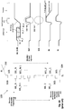
- Fig. 1 shows a stack of flash memory cells 100.
- the stack of flash memory cells 100 includes N transistors 101_1 through 101_N coupled along a vertical column whose respective gate structures correspond to individual storage elements.
- the column is accessed on the top side via a bit line (BL) 102 and source-gate-drain (SGD) transistor 103.
- Bias potentials are applied to the column through a bottom side source line (SL) 104 and a source-gate-source (SGS) transistor 105.
- bottom is understood to mean closer to the semiconductor chip substrate and top is understood to mean farther away from the semiconductor chip substrate.
- flash memory is written to (technically referred to as "programming") in units of blocks.
- a single block includes an array of flash cell stacks, where, storage cells residing at a same vertical position are tied to a same word line.
- a particular word line in the block is activated which, in turn, activates the cells of the various stacks that are coupled to that word line.
- the respective charges stored in the cells that are coupled to the activated word line influence the potential on their respective columns and bit lines which are then sensed to determine the read information (the cells that are not coupled to the activated word line are isolated from their respective columns).
- the respective bit lines of the stacks are charged consistently with the data to be programmed which, in turn, influences the potential of their respective columns.
- the cells that are coupled to the activated word line receive charge from their respective column which effectively programs these cells.
- the voltage placed on the activated word line is referred to as a "program voltage”.
- the cells that are not coupled to the activated word line do not receive the program voltage and are isolated from their columns during the program operation.
- Flash cells are programmed according to a "program-verify" process in which, after cells of a same word line are written to with new data using a particular word line voltage, the cells are then read back to confirm that each of their respective stored charge levels is consistent with the data that was intended to be written into them (verify). Those cells that fail (do not store sufficient charge) are then written to again but with a higher program voltage and again re-verified. Cells that pass are isolated from the re-write. The program-verify process then repeats successive iterations of program-verify operations with increasingly higher program voltage with each iteration until all cells that are tied to the activated word line are deemed to pass.
- program operations are applied to an entire block. As such, the above described process is performed for each word line in the block on a word line by word line basis. In a conventional programming approach, the word line by word line programming approach is performed sequentially moving up the column 110.
- cells coupled to the bottom most word line WL1 are first programmed according to the above described process. After the cells coupled to WL1 are fully programmed (all cells are deemed a pass after, e.g., successive program-verify iterations with increasing programming voltage applied to WL1 with each next program iteration), programming of cells coupled to WL2 begins. Cells coupled to WL2 are then programmed according to successive iterations of program-verify operations as described above. After all cells coupled to WL2 are deemed a pass, programming of cells coupled to WL3 begins. The process continues in sequence moving up the column in increasing word line order until cells coupled to the WL_N word line are fully programmed.
- the verifying of cells in between the program sequences of the program-verify iterations can result in the presence of unwanted, residue electrons in the block's respective columns.
- a process referred to as "extended verification recovery” (eVRCV) 111, 112 has been used as a final step of the verification sequence to remove these electrons.
- the block's word lines are driven to a low potential state in sequence moving up the columns from the bottom most word line to the top most word line 112. That is, first WL1 is driven to a low potential state, then, WL2 is driven to a low potential state, etc.
- Each lowering of word line potential drives electrons up the column away from the word line whose potential was just lowered.
- the lowering of word line potential then advances up the stack on a word line by word line basis.
- the potential of the topmost word line WL_N is finally lowered (with all lower word lines having their potential already lowered in sequence), all residue electrons that existed in the column after verification are pushed out of the column, onto the bit line 102 and subsequently absorbed.
- the traditional flash programming sequencing can be characterized as fully programming cells on a word line by word line basis moving up the column 110. That is, cells coupled to a next, immediately higher word line are not programmed until all cells of the current, immediately lower word line being programmed are deemed a "pass" after (typically) successive program-verify operations. Additionally, the succession of program-verify operations performed at each word line is characterized by performing "bottom-to-top" eVRCV 111, 112 as described above at the end of verification, and, injecting positive seed charge into the top of the column 113, 114, 115 from the bit line 102 just prior to programming at a next higher program voltage.
- a single flash cell is capable of storing more than two digital states to effect storage of more than one bit per cell.
- each cell is capable of storing sixteen different charge levels which, in turn, corresponds to the storage of four digital bits per cell.
- the distribution of charge amongst the cells needs to be fairly tight or precise for a same stored digital value. That is, if a number of flash cells are to store a same digital value, their respective stored charges should be nearly identical (there is a narrow charge spread amongst them). If it were it otherwise, it would be difficult if not impossible to read and write multi-state values into many different storage cells.
- the programming of a cell that is coupled to a particular word line can affect the stored charge levels of the cells that are coupled to its immediately neighboring word lines.
- the disturbance to the charge of the neighboring cells affectively increases the distribution/spread of charge across cells holding same values within the flash device.
- the program operation then proceeds to program cells coupled to word line WL_N-1. Again, a sequence of program-verify operations are performed to the cells that are coupled to word line WL_N-1 until they are deemed fully programmed, at which point cells coupled to WL_N-2 begin to be programmed. The process then continues in succession with cells coupled to each next lower word line being programmed until cells coupled to the bottom most word line WL_1 are programmed.
- the traditional extended verify operation is performed 111, 112. That is, as described at length above, at the end of each verification, electrons are pushed out of the column in the direction from the bottom of the column to the top of the column. To effect such electron movement, word line potentials are driven low in succession from the bottom most word line to the top most word line 112.
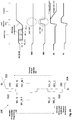
- ReVRCV reverse extended verification recovery
- seed charge enters the bottom of the column from the source line 204 through an activated SGS transistor 223. That is, upon remnant electrons being pushed out of the column in a top-to-bottom direction 221 through the SGS transistor 205 and on to the source line 204 at the end of the reverse order extended verify recovery operation 221, 222, the column is seeded 224, 225 with positive charge that flows from the source line 204 through the on SGS transistor 223 and into the bottom of the column. Positive charge that enters the bottom of the column 224 in this manner in able to reach the region of the column where the next word line to be programmed resides without passing by cells that have already been programmed.
- the seeding process can simultaneously attempt to send more seed charge into the top of the column 226 from the bit line 202 through an ON SGD transistor 228 as per the traditional approach.
- the injection efficiency is expected to be better with the bottom side injection than the top side injection for the reasons explained immediately above.
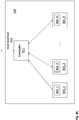
- Fig. 3a shows a flash memory chip 301 having one or more arrays of stacked storage cells (a three dimensional array of storage cells) 302 and an embedded controller logic circuit (also referred to as the chip's controller) 303.
- the embedded controller logic circuit 303 is designed to program the stacks of storage cells in reverse order (top-to-bottom), and, perform top-to-bottom extended verification recovery and bottom side seeding (with or without top side seeding) on the stacks as described at length above.
- the chip interface 304 is commonly used to receive access commands from a controller of a non volatile memory device.
- Fig. 3b shows a non volatile memory device 310 such as a memory module (e.g., a dual in-line memory (DIMM), a stacked memory module, etc.) or mass storage device (e.g., solid state drive (SDD)) having multiple flash memory chips 301_1 through 301_X whose blocks of flash cells are programmed in reverse order (top-to-bottom) and subjected to top-to-bottom extended verification recovery and bottom side seeding (with or without top side seeding) as described at length above.
- the non volatile memory device 310 includes a controller 311, and, each of the flash memory chips 301_1 through 301_X include an embedded controller logic circuit 303_1 through 303_X.
- the device controller 310 and/or the embedded flash memory chip controller logic circuits 303 are designed to cause the flash chips 301 to perform reverse order programming, top-to-bottom extended verification recovery (with top-to-bottom programming) and bottom side seeding (with or without top side seeding).
- the host interface 314 is commonly used to receive commands from (e.g., a peripheral control hub of) a larger host system such as a computer.
- the device controller 311 and/or embedded controller logic circuits 303 can be implemented with dedicated hardwired logic circuitry (e.g., Application Specific Integrated Circuit (ASIC) cell), programmable logic circuitry (e.g., Field Programmable Gate Array (FPGA) logic circuitry), and/or logic circuitry designed to execute some form of program code (e.g., firmware) such as an embedded processor.
- ASIC Application Specific Integrated Circuit
- FPGA Field Programmable Gate Array
- Fig. 4 provides an exemplary depiction of a computing system 400 (e.g., a smartphone, a tablet computer, a laptop computer, a desktop computer, a server computer, etc.).
- the basic computing system 400 may include a central processing unit 401 (which may include, e.g., a plurality of general-purpose processing cores 415_1 through 415_X) and the main memory controller 417 disposed on a multi-core processor or applications processor, system memory 402, a display 403 (e.g., touchscreen, flat-panel), a local wired point-to-point link (e.g., USB) interface 404, various network I/O functions 405 (such as an Ethernet interface and/or cellular modem subsystem), a wireless local area network (e.g., WiFi) interface 406, a wireless point-to-point link (e.g., Bluetooth) interface 407 and a Global Positioning System interface 408, various sensors 409_1 through 409_Y, one or more cameras
- An application processor or multi-core processor 450 may include one or more general-purpose processing cores 415 within its CPU 401, one or more graphical processing units 416, a memory management function 417 (e.g., a memory controller) and an I/O control function 418.
- the general-purpose processing cores 415 typically execute the system and application software of the computing system.
- the graphics processing unit 416 typically executes graphics intensive functions to, e.g., generate graphics information that is presented on the display 403.
- the memory control function 417 interfaces with the system memory 402 to write/read data to/from system memory 402.
- any of the system memory 402 and/or non volatile storage 420 can be composed with a three dimensional non volatile random access memory composed, e.g., of an emerging non volatile storage cell technology. Examples include Optane memory from Intel Corporation, QuantX from Micron Corporation, and/or other types of resistive non-volatile memory cells integrated amongst the interconnect wiring of a semiconductor chip (e.g., resistive random access memory (ReRAM), ferroelectric random access memory (FeRAM), spin transfer torque random access memory (STT-RAM), etc.).
- Mass storage 420 at least can also be composed of flash memory (e.g., NAND flash).
- the mass storage 420 or conceivably even system memory 402 if composed of non volatile (e.g., flash) memory, could be implemented with non volatile memory chips that program their storage cells in a direction along a stack of storage cells having less word line disturbances than the opposite direction and where the column connecting the cells in the stack is cleaned of charge in the same direction that the cells are programmed as described at length above, and where, seed charge prior to a next program iteration enters an end of the stack that is pointed to by the direction as described at length above .
- non volatile e.g., flash
- Each of the touchscreen display 403, the communication interfaces 404- 407, the GPS interface 408, the sensors 409, the camera(s) 410, and the speaker/microphone codec 413, 414 all can be viewed as various forms of I/O (input and/or output) relative to the overall computing system including, where appropriate, an integrated peripheral device as well (e.g., the one or more cameras 410).
- I/O components may be integrated on the applications processor/multi-core processor 450 or may be located off the die or outside the package of the applications processor/multi-core processor 450.
- the power management control unit 412 generally controls the power consumption of the system 400.
- Embodiments of the invention may include various processes as set forth above.
- the processes may be embodied in machine-executable instructions.
- the instructions can be used to cause a general-purpose or special-purpose processor to perform certain processes.
- these processes may be performed by specific/custom hardware components that contain hardwired logic circuitry or programmable logic circuitry (e.g., FPGA, PLD) for performing the processes, or by any combination of programmed computer components and custom hardware components.
- programmable logic circuitry e.g., FPGA, PLD
- Elements of the present invention may also be provided as a machine-readable medium for storing the machine-executable instructions.
- the machine-readable medium may include, but is not limited to, floppy diskettes, optical disks, CD-ROMs, and magneto-optical disks, FLASH memory, ROMs, RAMs, EPROMs, EEPROMs, magnetic or optical cards, propagation media or other type of media/machine-readable medium suitable for storing electronic instructions.
- the present invention may be downloaded as a computer program which may be transferred from a remote computer (e.g., a server) to a requesting computer (e.g., a client) by way of data signals embodied in a carrier wave or other propagation medium via a communication link (e.g., a modem or network connection).
- a remote computer e.g., a server
- a requesting computer e.g., a client
- a communication link e.g., a modem or network connection
Landscapes
- Engineering & Computer Science (AREA)
- Theoretical Computer Science (AREA)
- Human Computer Interaction (AREA)
- Physics & Mathematics (AREA)
- General Engineering & Computer Science (AREA)
- General Physics & Mathematics (AREA)
- Microelectronics & Electronic Packaging (AREA)
- Read Only Memory (AREA)
Abstract
Description
- The field of invention pertains generally to the electrical arts, and, more specifically, to a non volatile flash memory with improved verification recovery and column seeding.
- With the onset of "big-data", cloud-computing, artificial intelligence and other highly data intensive applications, the performance of non volatile memory is becoming an increasing focus of overall application performance because much of the data that is processed by these applications is ultimately read from and/or written to non volatile memory. As such, systems designers and non volatile memory chip and/or device designers are becoming increasingly focused on improving the performance of their non volatile memory chips and/or devices.
- A better understanding of the present invention can be obtained from the following detailed description in conjunction with the following drawings, in which:
-
Figs. 1A and1B show prior art processes of a prior art flash memory; -
Figs. 2A and2B show processes of an improved flash memory; -
Fig. 3a shows a non volatile memory chip; -
Fig. 3b shows a solid state drive; -
Fig. 4 shows a computing system. -
Fig. 1 shows a stack offlash memory cells 100. As observed inFig. 1 , the stack offlash memory cells 100 includes N transistors 101_1 through 101_N coupled along a vertical column whose respective gate structures correspond to individual storage elements. The column is accessed on the top side via a bit line (BL) 102 and source-gate-drain (SGD)transistor 103. Bias potentials are applied to the column through a bottom side source line (SL) 104 and a source-gate-source (SGS)transistor 105. Here, bottom is understood to mean closer to the semiconductor chip substrate and top is understood to mean farther away from the semiconductor chip substrate. - As is known in the art, flash memory is written to (technically referred to as "programming") in units of blocks. A single block includes an array of flash cell stacks, where, storage cells residing at a same vertical position are tied to a same word line. When reading from or writing to a particular page of information within a block, a particular word line in the block is activated which, in turn, activates the cells of the various stacks that are coupled to that word line. In the case of a read, the respective charges stored in the cells that are coupled to the activated word line influence the potential on their respective columns and bit lines which are then sensed to determine the read information (the cells that are not coupled to the activated word line are isolated from their respective columns).
- In the case of a write ("program"), the respective bit lines of the stacks are charged consistently with the data to be programmed which, in turn, influences the potential of their respective columns. The cells that are coupled to the activated word line receive charge from their respective column which effectively programs these cells. The voltage placed on the activated word line is referred to as a "program voltage". The cells that are not coupled to the activated word line do not receive the program voltage and are isolated from their columns during the program operation.
- Flash cells are programmed according to a "program-verify" process in which, after cells of a same word line are written to with new data using a particular word line voltage, the cells are then read back to confirm that each of their respective stored charge levels is consistent with the data that was intended to be written into them (verify). Those cells that fail (do not store sufficient charge) are then written to again but with a higher program voltage and again re-verified. Cells that pass are isolated from the re-write. The program-verify process then repeats successive iterations of program-verify operations with increasingly higher program voltage with each iteration until all cells that are tied to the activated word line are deemed to pass.
- Generally, program operations are applied to an entire block. As such, the above described process is performed for each word line in the block on a word line by word line basis. In a conventional programming approach, the word line by word line programming approach is performed sequentially moving up the
column 110. - That is, referring to
Fig. 1 , cells coupled to the bottom most word line WL1 are first programmed according to the above described process. After the cells coupled to WL1 are fully programmed (all cells are deemed a pass after, e.g., successive program-verify iterations with increasing programming voltage applied to WL1 with each next program iteration), programming of cells coupled to WL2 begins. Cells coupled to WL2 are then programmed according to successive iterations of program-verify operations as described above. After all cells coupled to WL2 are deemed a pass, programming of cells coupled to WL3 begins. The process continues in sequence moving up the column in increasing word line order until cells coupled to the WL_N word line are fully programmed. - The verifying of cells in between the program sequences of the program-verify iterations can result in the presence of unwanted, residue electrons in the block's respective columns. As such, a process referred to as "extended verification recovery" (eVRCV) 111, 112 has been used as a final step of the verification sequence to remove these electrons.
- In the case of traditional eVRCV, the block's word lines are driven to a low potential state in sequence moving up the columns from the bottom most word line to the top
most word line 112. That is, first WL1 is driven to a low potential state, then, WL2 is driven to a low potential state, etc. Each lowering of word line potential drives electrons up the column away from the word line whose potential was just lowered. The lowering of word line potential then advances up the stack on a word line by word line basis. Ideally, when the potential of the topmost word line WL_N is finally lowered (with all lower word lines having their potential already lowered in sequence), all residue electrons that existed in the column after verification are pushed out of the column, onto thebit line 102 and subsequently absorbed. - Commensurate with the formally ending of eVRCV is the "priming" of the column for programming by injecting positive "seed" charge (absorbing negative electrons) into the
column bit line 102 via anactive SGD transistor 115. - Thus, the traditional flash programming sequencing can be characterized as fully programming cells on a word line by word line basis moving up the
column 110. That is, cells coupled to a next, immediately higher word line are not programmed until all cells of the current, immediately lower word line being programmed are deemed a "pass" after (typically) successive program-verify operations. Additionally, the succession of program-verify operations performed at each word line is characterized by performing "bottom-to-top" eVRCV 111, 112 as described above at the end of verification, and, injecting positive seed charge into the top of thecolumn bit line 102 just prior to programming at a next higher program voltage. - As is known in the art, a single flash cell is capable of storing more than two digital states to effect storage of more than one bit per cell. For example, in the case of quad level cell (QLC), each cell is capable of storing sixteen different charge levels which, in turn, corresponds to the storage of four digital bits per cell. In order to successfully store multiple charge levels per cell, the distribution of charge amongst the cells needs to be fairly tight or precise for a same stored digital value. That is, if a number of flash cells are to store a same digital value, their respective stored charges should be nearly identical (there is a narrow charge spread amongst them). If it were it otherwise, it would be difficult if not impossible to read and write multi-state values into many different storage cells.
- Through an undesirable "disturb effect", the programming of a cell that is coupled to a particular word line can affect the stored charge levels of the cells that are coupled to its immediately neighboring word lines. The disturbance to the charge of the neighboring cells affectively increases the distribution/spread of charge across cells holding same values within the flash device.
- It has been observed, referring to
Fig. 1b , that the disturb effect can be reduced if cells are programmed on a word line by word line basis from top tobottom 116 rather than from bottom to top. That is, whereas, the traditional programming approach described just above programmed on a word-line by word line basis starting from the bottom of the column and advancing upward, in the improved "reverse order"approach 116, cells coupled to the topmost word line (WL_N) are programmed first in the sequential order. - After a sequence of program-verify operations that results in the cells coupled to word line WL_N being fully programmed, the program operation then proceeds to program cells coupled to word line WL_N-1. Again, a sequence of program-verify operations are performed to the cells that are coupled to word line WL_N-1 until they are deemed fully programmed, at which point cells coupled to WL_N-2 begin to be programmed. The process then continues in succession with cells coupled to each next lower word line being programmed until cells coupled to the bottom most word line WL_1 are programmed.
- According to known reverse order approaches, however, during the sequence of program-verify operations applied to any particular word line, the traditional extended verify operation is performed 111, 112. That is, as described at length above, at the end of each verification, electrons are pushed out of the column in the direction from the bottom of the column to the top of the column. To effect such electron movement, word line potentials are driven low in succession from the bottom most word line to the top
most word line 112. - Unfortunately, if electrons are pushed out of the column in a bottom to
top direction 111 during verification when reverse order programming is being applied 116, the electrons are pushed past cells that have already been fully programmed. That is, consider the initial programming of the cells that are coupled to the top most word line WL_N. Upon completion of the programming of these cells, and the following programming of cells coupled to the next lowest word line (WL_N-1), during the nominal bottom-to-top extended verifyrecovery sequence - Unfortunately, the charge levels that have been programmed into these cells (that are coupled to WL_N) can thwart the upward advancement of electrons up through the column. That is, the lowering of the potential of WL_N-1, by itself, can be insufficient to drive all electrons in the column past the cell coupled to the top word line WL_N and onto the
bit line 102. - A solution, referred to as "reverse extended verification recovery" (ReVRCV), is depicted in
Fig. 2A . In the case of ReVRCV, at the end of verification, the column is cleansed of residue electrons by pushing electrons in a top-down rather than bottom-updirection Fig. 2A , word line potentials are driven low in succession on a word line by word line basis starting with the top most word line (WL_N) and ending with the bottom most word line (WL_1) 222. By so doing, residue electrons in the column are easily pushed down thecolumn 221 past lower cells that have not yet been programmed. Upon being pushed past the cell that is coupled to the WL_1 word line, the electrons are pushed out of the bottom of the column through anON SGS transistor 223, onto thelower source line 204 and absorbed. - Recall from the discussion of
Figs. 1A and1B that thepriming bit line 102. Unfortunately, if the overall block is programmed in reverse order 220 (programming is performed on a word line by word line basis in a top to bottom direction), seed charge that attempts to enter the top of the column from thebit line 202 can be thwarted as it attempts to move past upper cells that have already been programmed. - That is, again, when programming the stack in
reverse order 220, cells coupled to upper word lines will be programmed ahead of cells that are coupled to lower word lines. As such, charge that attempts to enter the top of the column through the SGD transistor from thebit line 202 will need to pass by upper, already programmed cells in order to reach the region of the column where the cells that are yet to be programmed reside. Unfortunately, the stored charge levels of the already programmed upper cells can thwart the transfer of the positive charge as it attempts to flow through the upper region of the column from thebit line 202. - In order to overcome this problem, also observed in
Fig. 2A , seed charge enters the bottom of the column from thesource line 204 through an activatedSGS transistor 223. That is, upon remnant electrons being pushed out of the column in a top-to-bottom direction 221 through theSGS transistor 205 and on to thesource line 204 at the end of the reverse order extended verifyrecovery operation source line 204 through the onSGS transistor 223 and into the bottom of the column. Positive charge that enters the bottom of thecolumn 224 in this manner in able to reach the region of the column where the next word line to be programmed resides without passing by cells that have already been programmed. - Finally, as observed in
Fig. 2B , according to an additional embodiment, the seeding process can simultaneously attempt to send more seed charge into the top of thecolumn 226 from thebit line 202 through an ON SGDtransistor 228 as per the traditional approach. However, the injection efficiency is expected to be better with the bottom side injection than the top side injection for the reasons explained immediately above. -
Fig. 3a shows aflash memory chip 301 having one or more arrays of stacked storage cells (a three dimensional array of storage cells) 302 and an embedded controller logic circuit (also referred to as the chip's controller) 303. The embeddedcontroller logic circuit 303 is designed to program the stacks of storage cells in reverse order (top-to-bottom), and, perform top-to-bottom extended verification recovery and bottom side seeding (with or without top side seeding) on the stacks as described at length above. Thechip interface 304 is commonly used to receive access commands from a controller of a non volatile memory device. -
Fig. 3b shows a nonvolatile memory device 310 such as a memory module (e.g., a dual in-line memory (DIMM), a stacked memory module, etc.) or mass storage device (e.g., solid state drive (SDD)) having multiple flash memory chips 301_1 through 301_X whose blocks of flash cells are programmed in reverse order (top-to-bottom) and subjected to top-to-bottom extended verification recovery and bottom side seeding (with or without top side seeding) as described at length above. As observed inFig. 3b , the nonvolatile memory device 310 includes acontroller 311, and, each of the flash memory chips 301_1 through 301_X include an embedded controller logic circuit 303_1 through 303_X. Here, thedevice controller 310 and/or the embedded flash memory chipcontroller logic circuits 303 are designed to cause theflash chips 301 to perform reverse order programming, top-to-bottom extended verification recovery (with top-to-bottom programming) and bottom side seeding (with or without top side seeding). Thehost interface 314 is commonly used to receive commands from (e.g., a peripheral control hub of) a larger host system such as a computer. - The
device controller 311 and/or embeddedcontroller logic circuits 303 can be implemented with dedicated hardwired logic circuitry (e.g., Application Specific Integrated Circuit (ASIC) cell), programmable logic circuitry (e.g., Field Programmable Gate Array (FPGA) logic circuitry), and/or logic circuitry designed to execute some form of program code (e.g., firmware) such as an embedded processor. -
Fig. 4 provides an exemplary depiction of a computing system 400 (e.g., a smartphone, a tablet computer, a laptop computer, a desktop computer, a server computer, etc.). As observed inFIG. 4 , thebasic computing system 400 may include a central processing unit 401 (which may include, e.g., a plurality of general-purpose processing cores 415_1 through 415_X) and themain memory controller 417 disposed on a multi-core processor or applications processor,system memory 402, a display 403 (e.g., touchscreen, flat-panel), a local wired point-to-point link (e.g., USB)interface 404, various network I/O functions 405 (such as an Ethernet interface and/or cellular modem subsystem), a wireless local area network (e.g., WiFi)interface 406, a wireless point-to-point link (e.g., Bluetooth)interface 407 and a GlobalPositioning System interface 408, various sensors 409_1 through 409_Y, one ormore cameras 410, abattery 411, a powermanagement control unit 412, a speaker andmicrophone 413 and an audio coder/decoder 414. - An application processor or
multi-core processor 450 may include one or more general-purpose processing cores 415 within itsCPU 401, one or moregraphical processing units 416, a memory management function 417 (e.g., a memory controller) and an I/O control function 418. The general-purpose processing cores 415 typically execute the system and application software of the computing system. Thegraphics processing unit 416 typically executes graphics intensive functions to, e.g., generate graphics information that is presented on thedisplay 403. Thememory control function 417 interfaces with thesystem memory 402 to write/read data to/fromsystem memory 402. - Any of the
system memory 402 and/or non volatile storage 420 (also referred to as mass storage 420) can be composed with a three dimensional non volatile random access memory composed, e.g., of an emerging non volatile storage cell technology. Examples include Optane memory from Intel Corporation, QuantX from Micron Corporation, and/or other types of resistive non-volatile memory cells integrated amongst the interconnect wiring of a semiconductor chip (e.g., resistive random access memory (ReRAM), ferroelectric random access memory (FeRAM), spin transfer torque random access memory (STT-RAM), etc.).Mass storage 420 at least can also be composed of flash memory (e.g., NAND flash). - The
mass storage 420, or conceivably evensystem memory 402 if composed of non volatile (e.g., flash) memory, could be implemented with non volatile memory chips that program their storage cells in a direction along a stack of storage cells having less word line disturbances than the opposite direction and where the column connecting the cells in the stack is cleaned of charge in the same direction that the cells are programmed as described at length above, and where, seed charge prior to a next program iteration enters an end of the stack that is pointed to by the direction as described at length above . - Each of the
touchscreen display 403, the communication interfaces 404- 407, theGPS interface 408, thesensors 409, the camera(s) 410, and the speaker/microphone codec multi-core processor 450 or may be located off the die or outside the package of the applications processor/multi-core processor 450. The powermanagement control unit 412 generally controls the power consumption of thesystem 400. - Embodiments of the invention may include various processes as set forth above. The processes may be embodied in machine-executable instructions. The instructions can be used to cause a general-purpose or special-purpose processor to perform certain processes. Alternatively, these processes may be performed by specific/custom hardware components that contain hardwired logic circuitry or programmable logic circuitry (e.g., FPGA, PLD) for performing the processes, or by any combination of programmed computer components and custom hardware components.
- Elements of the present invention may also be provided as a machine-readable medium for storing the machine-executable instructions. The machine-readable medium may include, but is not limited to, floppy diskettes, optical disks, CD-ROMs, and magneto-optical disks, FLASH memory, ROMs, RAMs, EPROMs, EEPROMs, magnetic or optical cards, propagation media or other type of media/machine-readable medium suitable for storing electronic instructions. For example, the present invention may be downloaded as a computer program which may be transferred from a remote computer (e.g., a server) to a requesting computer (e.g., a client) by way of data signals embodied in a carrier wave or other propagation medium via a communication link (e.g., a modem or network connection).
- In the foregoing specification, the invention has been described with reference to specific exemplary embodiments thereof. It will, however, be evident that various modifications and changes may be made thereto without departing from the broader spirit and scope of the invention as set forth in the appended claims. The specification and drawings are, accordingly, to be regarded in an illustrative rather than a restrictive sense.
Claims (15)
- An apparatus, comprising:
a non volatile memory chip, comprising:an interface to receive access commands;a three dimensional array of non volatile storage cells; and,a controller to orchestrate removal of charge in a column of stacked ones of the non volatile storage cells after a verification process that determined whether or not a particular cell along the column was programmed with a correct charge amount, wherein the removal of the charge pushes the charge out of the column by changing respective word line potentials along a particular direction along the column, and wherein, cells that are coupled to the column are programmed in the particular direction, and wherein, disturbance of neighboring cells during programming is less along the particular direction than a direction opposite that of the particular direction. - The apparatus of claim 1 wherein the cells are flash cells.
- The apparatus of claim 1 wherein the direction is away from a bit line that is coupled to an end of the column.
- The apparatus of claim 3 wherein the bit line is coupled to a top end of the column.
- The apparatus of claim 1 wherein the direction is toward a bottom end of the column.
- The apparatus of claim 1 wherein the controller is also to seed the column with second charge that is opposite in polarity to the charge in the direction opposite that of the particular direction.
- The apparatus of claim 6 wherein the second charge is positive charge.
- The apparatus of claim 6 wherein the second charge is to flow through an on transistor positioned at an end of the column that is also not a storage cell transistor.
- The apparatus of claim 1 wherein the controller is at least partially implemented with logic circuitry .
- An apparatus, comprising:
a non volatile memory chip, comprising:an interface to receive access commands;a three dimensional array of non volatile storage cells; and,a controller to orchestrate seeding a column of stacked ones of the non volatile storage cells with charge in preparation for a next program iteration after a verification process that determined whether or not a particular cell along the column was programmed with a correct charge amount, wherein, cells that are coupled to the column are programmed in a particular direction along the column on a word line by word line basis, wherein, the particular direction points toward an end of the column where the seeding is injected, and wherein, disturbance of neighboring cells during programming is less along the particular direction than a direction opposite that of the particular direction. - The apparatus of claim 10 wherein the cells are flash cells.
- The apparatus of claim 10 wherein the direction is away from a bit line that is coupled to another opposite end of the column.
- The apparatus of claim 12 wherein the bit line is coupled to a top end of the column.
- The apparatus of claim 10 wherein the direction is toward a bottom end of the column.
- A computing system comprising the subject matter of any of claims 1 through 14.
Applications Claiming Priority (1)
| Application Number | Priority Date | Filing Date | Title |
|---|---|---|---|
| US16/808,955 US11621045B2 (en) | 2020-03-04 | 2020-03-04 | Non volatile flash memory with improved verification recovery and column seeding |
Publications (2)
| Publication Number | Publication Date |
|---|---|
| EP3876235A1 true EP3876235A1 (en) | 2021-09-08 |
| EP3876235B1 EP3876235B1 (en) | 2025-10-22 |
Family
ID=73475973
Family Applications (1)
| Application Number | Title | Priority Date | Filing Date |
|---|---|---|---|
| EP20208343.2A Active EP3876235B1 (en) | 2020-03-04 | 2020-11-18 | Non volatile flash memory with improved verification recovery and column seeding |
Country Status (3)
| Country | Link |
|---|---|
| US (1) | US11621045B2 (en) |
| EP (1) | EP3876235B1 (en) |
| KR (1) | KR20210112228A (en) |
Families Citing this family (5)
| Publication number | Priority date | Publication date | Assignee | Title |
|---|---|---|---|---|
| US11392325B2 (en) * | 2020-09-28 | 2022-07-19 | Quanta Computer Inc. | Method and system for parallel flash memory programming |
| EP4244894B1 (en) | 2020-12-15 | 2025-11-19 | Yangtze Memory Technologies Co., Ltd. | Architecture and method for nand memory operation |
| US12586646B2 (en) * | 2022-09-06 | 2026-03-24 | SanDisk Technologies, Inc. | Precharge scheme during programming of a memory device |
| KR20240129516A (en) * | 2023-02-20 | 2024-08-27 | 삼성전자주식회사 | Nonvolatile Memory Device And Operating Method of Nonvolatile Memory Device |
| US20250085863A1 (en) * | 2023-09-13 | 2025-03-13 | Micron Technology, Inc. | Managing an order of programming operations in a memory sub-system |
Citations (2)
| Publication number | Priority date | Publication date | Assignee | Title |
|---|---|---|---|---|
| US20190318784A1 (en) * | 2018-04-16 | 2019-10-17 | Samsung Electronics Co., Ltd. | Nonvolatile memory device and method of programming in the same |
| US20190378580A1 (en) * | 2018-06-07 | 2019-12-12 | Sandisk Technologies Llc | Non-volatile memory with countermeasure for program disturb including purge during precharge |
Family Cites Families (12)
| Publication number | Priority date | Publication date | Assignee | Title |
|---|---|---|---|---|
| JP4284300B2 (en) * | 2005-05-02 | 2009-06-24 | 株式会社東芝 | Semiconductor memory device |
| US7751245B2 (en) * | 2007-10-10 | 2010-07-06 | Micron Technology, Inc. | Programming sequence in NAND memory |
| US8120959B2 (en) * | 2008-05-30 | 2012-02-21 | Aplus Flash Technology, Inc. | NAND string based NAND/NOR flash memory cell, array, and memory device having parallel bit lines and source lines, having a programmable select gating transistor, and circuits and methods for operating same |
| KR102312404B1 (en) * | 2015-09-07 | 2021-10-13 | 에스케이하이닉스 주식회사 | Storage device and operating method thereof |
| JP6400547B2 (en) * | 2015-09-14 | 2018-10-03 | 東芝メモリ株式会社 | Memory device |
| US10585812B2 (en) * | 2016-03-30 | 2020-03-10 | Intel Corporation | Multi-standard single interface with reduced I/O count |
| JP2018147539A (en) * | 2017-03-08 | 2018-09-20 | 東芝メモリ株式会社 | Semiconductor memory device |
| KR102289598B1 (en) * | 2017-06-26 | 2021-08-18 | 삼성전자주식회사 | Non-volatile memory device and memory system including the same and program method thereof |
| KR102516121B1 (en) * | 2018-10-22 | 2023-03-31 | 에스케이하이닉스 주식회사 | Semiconductor device and operating method thereof |
| US10636498B1 (en) * | 2019-02-22 | 2020-04-28 | Sandisk Technologies Llc | Managing bit-line settling time in non-volatile memory |
| US10847234B2 (en) | 2019-04-26 | 2020-11-24 | Intel Corporation | Program verify technique for non-volatile memory |
| US10854304B1 (en) * | 2019-12-03 | 2020-12-01 | Micron Technology, Inc. | Apparatus and methods for seeding operations concurrently with data line set operations |
-
2020
- 2020-03-04 US US16/808,955 patent/US11621045B2/en active Active
- 2020-11-18 EP EP20208343.2A patent/EP3876235B1/en active Active
- 2020-11-26 KR KR1020200160882A patent/KR20210112228A/en active Pending
Patent Citations (2)
| Publication number | Priority date | Publication date | Assignee | Title |
|---|---|---|---|---|
| US20190318784A1 (en) * | 2018-04-16 | 2019-10-17 | Samsung Electronics Co., Ltd. | Nonvolatile memory device and method of programming in the same |
| US20190378580A1 (en) * | 2018-06-07 | 2019-12-12 | Sandisk Technologies Llc | Non-volatile memory with countermeasure for program disturb including purge during precharge |
Also Published As
| Publication number | Publication date |
|---|---|
| EP3876235B1 (en) | 2025-10-22 |
| US20210280261A1 (en) | 2021-09-09 |
| KR20210112228A (en) | 2021-09-14 |
| US11621045B2 (en) | 2023-04-04 |
Similar Documents
| Publication | Publication Date | Title |
|---|---|---|
| US11621045B2 (en) | Non volatile flash memory with improved verification recovery and column seeding | |
| US10699788B2 (en) | Non-volatile memory device and operating method thereof for performing an erase detect operation | |
| US11158381B2 (en) | Non-volatile memory device and operating method thereof | |
| KR102414186B1 (en) | Non-volatile memory device and program method thereof | |
| US10573378B2 (en) | Methods of programming memory devices | |
| JP7222632B2 (en) | MEMORY DEVICE INCLUDING WORDLINE FAILURE DETECTION CIRCUIT AND DRIVING METHOD THEREOF | |
| CN103219040B (en) | Nonvolatile semiconductor memory member and storage system and its programmed method and control method | |
| CN108511023B (en) | Semiconductor memory device and method of operating the same | |
| CN105321567B (en) | Nonvolatile memory device, programming method, and storage device | |
| US10360978B2 (en) | Semiconductor memory device for performing coding program and operating method thereof | |
| CN109785892B (en) | Memory device including word line defect detection circuit | |
| US20190378580A1 (en) | Non-volatile memory with countermeasure for program disturb including purge during precharge | |
| TWI874472B (en) | Semiconductor memory device and method of operating the same | |
| US10311956B2 (en) | Semiconductor memory device and operating method thereof | |
| KR20170129516A (en) | Semiconductor memory device and operating method thereof | |
| US12165721B2 (en) | Nonvolatile memory device and operation method of detecting defective memory cells | |
| US10847234B2 (en) | Program verify technique for non-volatile memory | |
| CN117079682A (en) | Memory device configured to reduce verification time and method of operating same | |
| US12136453B2 (en) | Systems, methods and media of optimization of temporary read errors in 3D NAND memory devices | |
| US12633355B2 (en) | Program refresh for all levels program operation in a memory device | |
| US12322455B2 (en) | Program verify process having placement aware pre-program verify (PPV) bucket size modulation | |
| US20250285683A1 (en) | Methods and apparatuses for operating a memory device | |
| US20250364059A1 (en) | Flash memory having improved performance as a consequence of program direction along a flash storage cell column | |
| US20260031157A1 (en) | Program refresh for all levels program operation in a memory device | |
| CN115376597A (en) | Programming method of memory, memory and storage system |
Legal Events
| Date | Code | Title | Description |
|---|---|---|---|
| PUAI | Public reference made under article 153(3) epc to a published international application that has entered the european phase |
Free format text: ORIGINAL CODE: 0009012 |
|
| STAA | Information on the status of an ep patent application or granted ep patent |
Free format text: STATUS: THE APPLICATION HAS BEEN PUBLISHED |
|
| AK | Designated contracting states |
Kind code of ref document: A1 Designated state(s): AL AT BE BG CH CY CZ DE DK EE ES FI FR GB GR HR HU IE IS IT LI LT LU LV MC MK MT NL NO PL PT RO RS SE SI SK SM TR |
|
| STAA | Information on the status of an ep patent application or granted ep patent |
Free format text: STATUS: REQUEST FOR EXAMINATION WAS MADE |
|
| 17P | Request for examination filed |
Effective date: 20220304 |
|
| RBV | Designated contracting states (corrected) |
Designated state(s): AL AT BE BG CH CY CZ DE DK EE ES FI FR GB GR HR HU IE IS IT LI LT LU LV MC MK MT NL NO PL PT RO RS SE SI SK SM TR |
|
| RAP1 | Party data changed (applicant data changed or rights of an application transferred) |
Owner name: INTEL NDTM US LLC |
|
| STAA | Information on the status of an ep patent application or granted ep patent |
Free format text: STATUS: EXAMINATION IS IN PROGRESS |
|
| 17Q | First examination report despatched |
Effective date: 20250103 |
|
| GRAP | Despatch of communication of intention to grant a patent |
Free format text: ORIGINAL CODE: EPIDOSNIGR1 |
|
| STAA | Information on the status of an ep patent application or granted ep patent |
Free format text: STATUS: GRANT OF PATENT IS INTENDED |
|
| INTG | Intention to grant announced |
Effective date: 20250519 |
|
| GRAS | Grant fee paid |
Free format text: ORIGINAL CODE: EPIDOSNIGR3 |
|
| GRAA | (expected) grant |
Free format text: ORIGINAL CODE: 0009210 |
|
| STAA | Information on the status of an ep patent application or granted ep patent |
Free format text: STATUS: THE PATENT HAS BEEN GRANTED |
|
| AK | Designated contracting states |
Kind code of ref document: B1 Designated state(s): AL AT BE BG CH CY CZ DE DK EE ES FI FR GB GR HR HU IE IS IT LI LT LU LV MC MK MT NL NO PL PT RO RS SE SI SK SM TR |
|
| P01 | Opt-out of the competence of the unified patent court (upc) registered |
Free format text: CASE NUMBER: UPC_APP_7233_3876235/2025 Effective date: 20250916 |
|
| REG | Reference to a national code |
Ref country code: CH Ref legal event code: F10 Free format text: ST27 STATUS EVENT CODE: U-0-0-F10-F00 (AS PROVIDED BY THE NATIONAL OFFICE) Effective date: 20251022 Ref country code: GB Ref legal event code: FG4D |
|
| REG | Reference to a national code |
Ref country code: DE Ref legal event code: R096 Ref document number: 602020060761 Country of ref document: DE |
|
| REG | Reference to a national code |
Ref country code: IE Ref legal event code: FG4D |
|
| REG | Reference to a national code |
Ref country code: NL Ref legal event code: FP |
|
| PG25 | Lapsed in a contracting state [announced via postgrant information from national office to epo] |
Ref country code: ES Free format text: LAPSE BECAUSE OF FAILURE TO SUBMIT A TRANSLATION OF THE DESCRIPTION OR TO PAY THE FEE WITHIN THE PRESCRIBED TIME-LIMIT Effective date: 20251022 |
|
| REG | Reference to a national code |
Ref country code: LT Ref legal event code: MG9D |
|
| PG25 | Lapsed in a contracting state [announced via postgrant information from national office to epo] |
Ref country code: NO Free format text: LAPSE BECAUSE OF FAILURE TO SUBMIT A TRANSLATION OF THE DESCRIPTION OR TO PAY THE FEE WITHIN THE PRESCRIBED TIME-LIMIT Effective date: 20260122 |
|
| PG25 | Lapsed in a contracting state [announced via postgrant information from national office to epo] |
Ref country code: FI Free format text: LAPSE BECAUSE OF FAILURE TO SUBMIT A TRANSLATION OF THE DESCRIPTION OR TO PAY THE FEE WITHIN THE PRESCRIBED TIME-LIMIT Effective date: 20251022 Ref country code: HR Free format text: LAPSE BECAUSE OF FAILURE TO SUBMIT A TRANSLATION OF THE DESCRIPTION OR TO PAY THE FEE WITHIN THE PRESCRIBED TIME-LIMIT Effective date: 20251022 Ref country code: AT Free format text: LAPSE BECAUSE OF FAILURE TO SUBMIT A TRANSLATION OF THE DESCRIPTION OR TO PAY THE FEE WITHIN THE PRESCRIBED TIME-LIMIT Effective date: 20251022 |
|
| REG | Reference to a national code |
Ref country code: AT Ref legal event code: MK05 Ref document number: 1849947 Country of ref document: AT Kind code of ref document: T Effective date: 20251022 |
|
| PG25 | Lapsed in a contracting state [announced via postgrant information from national office to epo] |
Ref country code: RS Free format text: LAPSE BECAUSE OF FAILURE TO SUBMIT A TRANSLATION OF THE DESCRIPTION OR TO PAY THE FEE WITHIN THE PRESCRIBED TIME-LIMIT Effective date: 20260122 |
|
| PG25 | Lapsed in a contracting state [announced via postgrant information from national office to epo] |
Ref country code: IS Free format text: LAPSE BECAUSE OF FAILURE TO SUBMIT A TRANSLATION OF THE DESCRIPTION OR TO PAY THE FEE WITHIN THE PRESCRIBED TIME-LIMIT Effective date: 20260222 |
|
| PG25 | Lapsed in a contracting state [announced via postgrant information from national office to epo] |
Ref country code: PT Free format text: LAPSE BECAUSE OF FAILURE TO SUBMIT A TRANSLATION OF THE DESCRIPTION OR TO PAY THE FEE WITHIN THE PRESCRIBED TIME-LIMIT Effective date: 20260223 |
|
| PG25 | Lapsed in a contracting state [announced via postgrant information from national office to epo] |
Ref country code: PL Free format text: LAPSE BECAUSE OF FAILURE TO SUBMIT A TRANSLATION OF THE DESCRIPTION OR TO PAY THE FEE WITHIN THE PRESCRIBED TIME-LIMIT Effective date: 20251022 |
|
| PG25 | Lapsed in a contracting state [announced via postgrant information from national office to epo] |
Ref country code: LV Free format text: LAPSE BECAUSE OF FAILURE TO SUBMIT A TRANSLATION OF THE DESCRIPTION OR TO PAY THE FEE WITHIN THE PRESCRIBED TIME-LIMIT Effective date: 20251022 |
|
| PG25 | Lapsed in a contracting state [announced via postgrant information from national office to epo] |
Ref country code: BG Free format text: LAPSE BECAUSE OF FAILURE TO SUBMIT A TRANSLATION OF THE DESCRIPTION OR TO PAY THE FEE WITHIN THE PRESCRIBED TIME-LIMIT Effective date: 20251022 |